WO2015029705A1 - 半導体エネルギー線検出素子 - Google Patents
半導体エネルギー線検出素子 Download PDFInfo
- Publication number
- WO2015029705A1 WO2015029705A1 PCT/JP2014/070482 JP2014070482W WO2015029705A1 WO 2015029705 A1 WO2015029705 A1 WO 2015029705A1 JP 2014070482 W JP2014070482 W JP 2014070482W WO 2015029705 A1 WO2015029705 A1 WO 2015029705A1
- Authority
- WO
- WIPO (PCT)
- Prior art keywords
- semiconductor
- semiconductor region
- region
- conductivity type
- main surface
- Prior art date
- Legal status (The legal status is an assumption and is not a legal conclusion. Google has not performed a legal analysis and makes no representation as to the accuracy of the status listed.)
- Ceased
Links
Images



Classifications
-
- G—PHYSICS
- G01—MEASURING; TESTING
- G01T—MEASUREMENT OF NUCLEAR OR X-RADIATION
- G01T1/00—Measuring X-radiation, gamma radiation, corpuscular radiation, or cosmic radiation
- G01T1/16—Measuring radiation intensity
- G01T1/24—Measuring radiation intensity with semiconductor detectors
-
- H—ELECTRICITY
- H10—SEMICONDUCTOR DEVICES; ELECTRIC SOLID-STATE DEVICES NOT OTHERWISE PROVIDED FOR
- H10F—INORGANIC SEMICONDUCTOR DEVICES SENSITIVE TO INFRARED RADIATION, LIGHT, ELECTROMAGNETIC RADIATION OF SHORTER WAVELENGTH OR CORPUSCULAR RADIATION
- H10F39/00—Integrated devices, or assemblies of multiple devices, comprising at least one element covered by group H10F30/00, e.g. radiation detectors comprising photodiode arrays
- H10F39/10—Integrated devices
- H10F39/107—Integrated devices having multiple elements covered by H10F30/00 in a repetitive configuration, e.g. radiation detectors comprising photodiode arrays
-
- H—ELECTRICITY
- H10—SEMICONDUCTOR DEVICES; ELECTRIC SOLID-STATE DEVICES NOT OTHERWISE PROVIDED FOR
- H10F—INORGANIC SEMICONDUCTOR DEVICES SENSITIVE TO INFRARED RADIATION, LIGHT, ELECTROMAGNETIC RADIATION OF SHORTER WAVELENGTH OR CORPUSCULAR RADIATION
- H10F39/00—Integrated devices, or assemblies of multiple devices, comprising at least one element covered by group H10F30/00, e.g. radiation detectors comprising photodiode arrays
- H10F39/80—Constructional details of image sensors
- H10F39/809—Constructional details of image sensors of hybrid image sensors
Definitions
- the present invention relates to a semiconductor energy ray detecting element for detecting energy rays including high energy radiation such as ⁇ rays or X rays, ultraviolet rays, visible light, infrared rays and the like.
- a semiconductor substrate having a first main surface and a second main surface facing each other, wherein the semiconductor substrate is on a first main surface side of the first conductivity type located on the first main surface side;
- a second semiconductor region of a first conductivity type that is located and has a higher impurity concentration than the first semiconductor region, and is located on the first main surface side and constitutes an energy beam sensitive region with the second semiconductor region;
- a semiconductor energy ray detecting element having a conductive third semiconductor region is known (for example, see Patent Document 1).
- the semiconductor substrate further includes a first conductivity type outer edge semiconductor region which is located along the outer edge of the semiconductor substrate on the first main surface side and has a higher impurity concentration than the first semiconductor region. The outer edge semiconductor region suppresses the depletion layer from reaching the side surface.
- a high bias voltage for example, about several hundred to one thousand volts
- the first semiconductor region needs to be in a fully depleted state in which a depletion layer extending from the third semiconductor region reaches the interface with the second semiconductor region from the first main surface side.
- a high bias voltage is applied to the semiconductor energy ray detection element, the following problems may occur.
- a ROIC (Read-out IC) chip that reads a signal from the semiconductor energy ray detection element is connected to the semiconductor energy ray detection element.
- the semiconductor energy ray detection element and the ROIC chip are arranged close to each other because the corresponding electrodes are bump-connected.
- the outer edge semiconductor region has the same conductivity type as the first semiconductor region, so that the potential of the outer edge semiconductor region is as high as the first semiconductor region. Become. For this reason, the potential difference between the ROIC chip and the outer edge semiconductor region is large, and electric discharge tends to occur between the outer edge semiconductor region and the ROIC chip.
- the electric field tends to concentrate due to the shape (angular shape) of the outer edge of the semiconductor substrate, and electric discharge is likely to occur. If a discharge is generated between the ROIC chip and the semiconductor energy ray detecting element, the element may be destroyed.
- An object of the present invention is to provide a semiconductor energy ray detection element capable of suppressing the occurrence of discharge.
- One aspect of the present invention is a semiconductor energy beam detection element including a semiconductor substrate having a first main surface and a second main surface facing each other, the semiconductor substrate being a first main surface located on the first main surface side.
- the first semiconductor region of the conductivity type and the second semiconductor region located on the second main surface side and having a higher impurity concentration than the first semiconductor region, the first semiconductor region located on the first main surface side, the first The second conductivity type, which is located so as to surround the periphery of the region where the third semiconductor region is located on the first main surface side, and the third semiconductor region of the second conductivity type constituting the energy ray sensitive region with the semiconductor region A fourth semiconductor region, and a fifth semiconductor region of the second conductivity type located along the outer edge of the semiconductor substrate on the first main surface side.
- the semiconductor substrate has a fifth semiconductor region located along the outer edge of the semiconductor substrate on the first main surface side. Since the fifth semiconductor region has a second conductivity type different from the conductivity type of the first semiconductor region, a PN barrier is formed between the first semiconductor region and the fifth semiconductor region.
- a high bias voltage is applied to the semiconductor energy ray detection element, a voltage drop occurs due to the PN barrier formed between the first semiconductor region and the fifth semiconductor region, and the potential of the fifth semiconductor region becomes the first semiconductor region. It falls below the potential of the region. Therefore, the potential difference between the semiconductor substrate (fifth semiconductor region) and the ROIC chip is small, and electric discharge is unlikely to occur between the semiconductor substrate and the ROIC chip.
- discharge is likely to occur at the outer edge of the semiconductor substrate, and a discharge path (current path) is likely to be formed along the side surface of the semiconductor substrate.
- a discharge path current path
- the PN barrier formed between the first semiconductor region and the fifth semiconductor region is located on this current path, it is difficult for current to flow through the current path. This also makes it difficult for discharge to occur between the semiconductor substrate and the ROIC chip.
- the semiconductor substrate is located between the fourth semiconductor region and the fifth semiconductor region so as to surround the fourth semiconductor region on the first main surface side, and has a higher impurity concentration than the first semiconductor region.
- a semiconductor region of the first conductivity type may be further included. In this case, the depletion layer is prevented from reaching the side surface of the semiconductor substrate in a state where the first semiconductor region is completely depleted.
- the semiconductor substrate further includes a first conductivity type semiconductor region located on the side surface so that the first semiconductor region is not exposed on the side surface of the semiconductor substrate and having a higher impurity concentration than the first semiconductor region. May be.
- the depletion layer is prevented from reaching the side surface of the semiconductor substrate in a state where the first semiconductor region is completely depleted.
- the semiconductor energy ray detection element is disposed so as to cover the surface of the first semiconductor region exposed as the side surface of the semiconductor substrate, and a fixed charge having a predetermined polarity exists on the surface side of the covered first semiconductor region.
- a film made of a passivation material may be further provided.
- a fixed charge having a predetermined polarity exists on the surface side of the first semiconductor region covered with the film made of the passivation material.
- the region on the surface side of the first semiconductor region where a fixed charge of a predetermined polarity exists functions as an accumulation layer. Since the film made of the passivation material is positioned on the side surface so that the first semiconductor region is not exposed to the side surface, the depletion layer is reliably suppressed from reaching the side surface of the semiconductor substrate.
- the first conductivity type is P-type
- the second conductivity type is N-type
- passivation material may be Al 2 O 3.
- positive fixed charges exist on the surface side of the first semiconductor region covered with the film made of the passivation material.
- the semiconductor energy ray detection element is disposed so as to cover the surface of the first semiconductor region exposed in the region between the second semiconductor region and the third semiconductor region as the first main surface of the semiconductor substrate.
- a film made of a passivation material for allowing a fixed charge having a predetermined polarity to exist on the surface side of the first semiconductor region may be further provided.
- a fixed charge having a predetermined polarity exists on the surface side of the first semiconductor region covered with the film made of the passivation material.
- the region on the surface side of the first semiconductor region where a fixed charge of a predetermined polarity exists functions as an accumulation layer. Since the film made of the passivation material is disposed so as to cover the surface of the first semiconductor region exposed in the region between the second semiconductor region and the third semiconductor region, the depletion layer reaches the side surface of the semiconductor substrate. To be suppressed.
- the first conductivity type may be N type
- the second conductivity type may be P type
- the passivation material may be SiO 2 or Si 3 N 4 .
- a negative fixed charge exists on the surface side of the first semiconductor region covered with the film made of the passivation material.
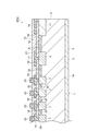
- FIG. 1 is a diagram for explaining a cross-sectional configuration of a semiconductor energy ray detection element according to an embodiment.
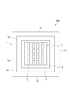
- FIG. 2 is a plan view of the semiconductor energy ray detection element according to the present embodiment.
- FIG. 3 is a diagram for explaining a cross-sectional configuration of the semiconductor energy ray detection element according to the first modification of the present embodiment.
- FIG. 4 is a diagram for explaining a cross-sectional configuration of a semiconductor energy ray detection element according to a second modification of the present embodiment.
- FIG. 5 is a plan view of a semiconductor energy ray detection element according to the second modification.
- FIG. 6 is a diagram for explaining a cross-sectional configuration of a semiconductor energy ray detection element according to a third modification of the present embodiment.
- FIG. 1 is a diagram for explaining a cross-sectional configuration of a semiconductor energy ray detection element according to an embodiment.
- FIG. 2 is a plan view of the semiconductor energy ray detection element according to the present embodiment.
- FIG. 3 is
- FIG. 7 is a diagram for explaining a cross-sectional configuration of a semiconductor energy ray detection element according to a fourth modification of the present embodiment.
- FIG. 8 is a diagram for explaining a cross-sectional configuration of a semiconductor energy beam detection element according to a fifth modification of the present embodiment.
- FIG. 1 is a diagram for explaining a cross-sectional configuration of the semiconductor energy beam detection element according to the present embodiment.
- FIG. 2 is a plan view of the semiconductor energy ray detection element according to the present embodiment. In FIG. 2, illustration of an insulating film 13, electrodes 15, 17, 19, a passivation film 21, and a bump electrode 23 described later is omitted.
- the semiconductor energy ray detection element ED1 includes a semiconductor substrate 1 as shown in FIG.
- the semiconductor substrate 1 is a first conductivity type (for example, P type) silicon substrate having a pair of main surfaces 1a and 1b and a side surface 1c facing each other.
- the side surface 1c extends in the opposing direction of the pair of main surfaces 1a and 1b so as to connect the pair of main surfaces 1a and 1b.
- the semiconductor substrate 1 has a rectangular shape in plan view and has four side surfaces 1c.
- the semiconductor substrate 1 includes a first semiconductor region 3 of a first conductivity type (for example, P type) located on the main surface 1a side and a second of a first conductivity type (for example, P type) located on the main surface 1b side. And a semiconductor region 5.
- the second semiconductor region 5 is a region to which a first conductivity type impurity (such as boron) is added, and has an impurity concentration higher than that of the first semiconductor region 3.
- the second semiconductor region 5 is formed by adding a first conductivity type impurity from the main surface 1b side to the semiconductor substrate 1 by, for example, ion implantation or diffusion.
- the semiconductor substrate 1 has a plurality of second conductivity type (for example, N-type) third semiconductor regions 7 on the main surface 1a side of the semiconductor substrate 1 (first semiconductor region 3). A part of the first semiconductor region 3 is interposed between the third semiconductor regions 7. That is, the third semiconductor regions 7 are separated from each other.
- Each third semiconductor region 7 is a region to which a second conductivity type impurity (such as antimony, arsenic, or phosphorus) is added, and has a higher impurity concentration than the first semiconductor region 3.
- a second conductivity type impurity such as antimony, arsenic, or phosphorus
- a PN junction is formed by the first semiconductor region 3 and each third semiconductor region 7. That is, each third semiconductor region 7 forms an energy ray sensitive region with the first semiconductor region 3.
- the semiconductor substrate 1 has fourth and fifth semiconductor regions 9 and 11 of the second conductivity type (for example, N type) on the main surface 1a side of the semiconductor substrate 1 (first semiconductor region 3).
- the fourth and fifth semiconductor regions 9 and 11 are regions to which a second conductivity type impurity (such as antimony, arsenic, or phosphorus) is added, and the impurity concentration is higher than that of the first semiconductor region 3.
- a second conductivity type impurity such as antimony, arsenic, or phosphorus
- the fourth semiconductor region 9 is positioned so as to surround the periphery of the region where the plurality of third semiconductor regions 7 are located when viewed from the opposing direction of the main surface 1a and the main surface 1b. Yes.
- the fourth semiconductor region 9 functions as a guard ring.
- a partial region of the first semiconductor region 3 is interposed between the third semiconductor region 7 and the fourth semiconductor region 9. That is, the third semiconductor region 7 and the fourth semiconductor region 9 are separated from each other.
- the fifth semiconductor region 11 is located along the outer edge of the semiconductor substrate 1 on the main surface 1a side.
- the fourth semiconductor region 9 is located between the region where the plurality of third semiconductor regions 7 are located and the fifth semiconductor region 11. That is, the fifth semiconductor region 11 is positioned so as to surround the fourth semiconductor region 9 when viewed from the opposing direction of the main surface 1a and the main surface 1b.
- Part of the first semiconductor region 3 is interposed between the fourth semiconductor region 9 and the fifth semiconductor region 11. That is, the fourth semiconductor region 9 and the fifth semiconductor region 11 are separated from each other.
- the third, fourth, and fifth semiconductor regions 7, 9, and 11 are formed by adding a second conductivity type impurity from the main surface 1a side to the semiconductor substrate 1 by, for example, an ion implantation method or a diffusion method.
- an insulating film 13 and electrodes 15, 17, 19 are disposed on the semiconductor substrate 1.
- the insulating film 13 is disposed on the main surface 1 a side of the semiconductor substrate 1 so as to cover the main surface 1 a of the semiconductor substrate 1.
- the insulating film 13 is made of, for example, SiO 2 .
- the insulating film 13 is formed by, for example, a thermal oxidation method, a sputtering method, or a PECVD (Plasma-enhanced Chemical Vapor Deposition) method.
- the electrodes 15, 17, 19 are formed for the corresponding semiconductor regions 7, 9, 11 after removing a part of the insulating film 13 formed on the semiconductor regions 7, 9, 11.
- the electrode 15 is connected to the third semiconductor region 7
- the electrode 17 is connected to the fourth semiconductor region 9
- the electrode 19 is connected to the fifth semiconductor region 11.
- the electrodes 15, 17, 19 are made of an electrode material such as aluminum.
- an electrode connected to the second semiconductor region 5 is also formed on the main surface 1 b side of the semiconductor substrate 1.
- the semiconductor substrate 1 is further provided with a passivation film 21 and a bump electrode 23.
- the passivation film 21 is disposed on the main surface 1 a side of the semiconductor substrate 1 so as to cover the insulating film 13 and the electrodes 15, 17, 19.
- the passivation film 21 is made of SiN, for example.
- the passivation film 21 is formed by, for example, a CVD (Chemical Vapor Deposition) method.
- the bump electrode 23 is formed for each corresponding third semiconductor region 7 after removing a part of the passivation film 21 formed on the third semiconductor region 7.
- the bump electrode 23 is electrically connected to the corresponding electrode 15.
- the bump electrode 23 is made of, for example, Sn—Ag. As a method for forming the bump electrode 23, a method of mounting a solder ball or a printing method can be used.
- the electrodes 17 and 19 are covered with a passivation film 21.
- the semiconductor energy ray detection element ED1 is mounted on the ROIC chip RC as shown in FIG. Specifically, the semiconductor energy ray detection element ED1 is bump-connected to the ROIC chip RC.
- the ROIC chip RC includes a plurality of pad electrodes 25, and the corresponding pad electrodes 25 and bump electrodes 23 are connected.
- the semiconductor energy ray detection element ED1 and the ROIC chip RC are arranged close to each other.
- the main surface 1a of the semiconductor substrate 1 faces the ROIC chip RC.
- a depletion is performed from the third semiconductor region 7 to the first semiconductor region 3 by applying a bias voltage (reverse bias voltage) between the second semiconductor region 5 and the third semiconductor region 7.
- the layer expands.
- a state where the depletion layer reaches the second semiconductor region 5 is a completely depleted state.
- the semiconductor substrate 1 has the fifth semiconductor region 11 positioned along the outer edge of the semiconductor substrate 1 on the main surface 1a side. Since the fifth semiconductor region 11 has a second conductivity type different from the conductivity type of the first semiconductor region 3, a PN barrier is formed between the first semiconductor region 3 and the fifth semiconductor region.
- a high bias voltage for example, about several hundred to one thousand volts
- the voltage is caused by the PN barrier formed between the first semiconductor region 3 and the fifth semiconductor region 11.
- a drop occurs, and the potential of the fifth semiconductor region 11 falls below the potential of the first semiconductor region 3. Therefore, the potential difference between the semiconductor substrate 1 (fifth semiconductor region 11) and the ROIC chip RC is small, and electric discharge is unlikely to occur between the semiconductor substrate 1 and the ROIC chip RC.
- the semiconductor energy beam detection element ED1 can suppress the occurrence of discharge. It is possible to suppress the depletion layer from reaching the side surface 1c by setting the distance between the fourth semiconductor region 9 and the fifth semiconductor region 11 to a predetermined value.
- a configuration for suppressing discharge between the semiconductor substrate and the ROIC chip a configuration in which the potential difference between the semiconductor substrate and the ROIC chip is reduced is conceivable.
- a double-sided structure in which the potential on the pair of main surfaces is approximately the same as the potential of the ROIC chip at the end of the semiconductor substrate may be adopted for the semiconductor energy ray detection element.
- the above-described manufacturing process can be prevented from becoming complicated and expensive.
- a configuration in which an insulating resin is filled between the end portion of the semiconductor substrate and the ROIC chip can be considered as a countermeasure against discharge.
- the step of filling the insulating resin needs to be added when the semiconductor energy ray detection is mounted on the ROIC chip or after the mounting, the manufacturing process becomes complicated as a result. Inevitable.
- the semiconductor energy ray detection element ED1 of the present embodiment since the semiconductor substrate 1 has the fifth semiconductor region 11, the occurrence of discharge is suppressed, so that the manufacturing process is complicated and the cost is high. There is no inconvenience.
- FIG. 3 is a diagram for explaining a cross-sectional configuration of the semiconductor energy ray detection element according to the first modification of the present embodiment.
- the semiconductor substrate 1 has a first conductivity type (for example, P-type) semiconductor region 31 on the main surface 1a side of the semiconductor substrate 1 (first semiconductor region 3).
- the semiconductor region 31 is located between the fourth semiconductor region 9 and the fifth semiconductor region 11 so as to surround the fourth semiconductor region 9 when viewed from the opposing direction of the main surface 1a and the main surface 1b.
- the semiconductor region 31 is a region to which an impurity of the first conductivity type (boron or the like) is added, and has an impurity concentration higher than that of the first semiconductor region 3.
- the semiconductor region 31 is in contact with the fourth semiconductor region 9 and the fifth semiconductor region 11. For this reason, the impurity concentration in the semiconductor region 31 is preferably lower than the impurity concentration in the third, fourth, and fifth semiconductor regions 7, 9, 11.
- the thickness of the semiconductor region 31 is smaller than the thickness of the third, fourth, and fifth semiconductor regions 7, 9, 11.
- the semiconductor region 31 is formed by, for example, an ion implantation method.
- the semiconductor region 31 is formed by an ion implantation method without using a mask in which a predetermined opening is formed, the first semiconductor region 3 exposed as the main surface 1a of the semiconductor substrate 1 is exposed on the surface side of the first semiconductor region 3.
- a conductive type (for example, P type) semiconductor region 33 is also formed.
- the semiconductor regions 33 are formed between the third semiconductor regions 7 and between the third semiconductor region 7 and the fourth semiconductor region 9, respectively.
- a region where impurities of the first conductivity type (for example, P-type) exist also on the surface side of the third, fourth, and fifth semiconductor regions 7, 9, 11 exposed as the main surface 1a of the semiconductor substrate 1 35 is formed.
- the impurity concentrations in the semiconductor regions 31 and 33 are set lower than the impurity concentrations in the third, fourth, and fifth semiconductor regions 7, 9, and 11, so that the third, fourth, and fifth. It is possible to suppress the occurrence of trouble in the functions of the semiconductor regions 7, 9, and 11.
- the semiconductor substrate 1 is located between the fourth semiconductor region 9 and the fifth semiconductor region 11 so as to surround the periphery of the fourth semiconductor region 9 on the main surface 1 a side, and from the first semiconductor region 3.
- the semiconductor region 31 of the first conductivity type having a high impurity concentration This suppresses the depletion layer from reaching the side surface 1c of the semiconductor substrate 1 in a state where the first semiconductor region 3 is completely depleted.
- FIG. 4 is a diagram for explaining a cross-sectional configuration of a semiconductor energy ray detection element according to a second modification of the present embodiment.
- FIG. 5 is a plan view of a semiconductor energy ray detection element according to the second modification.
- illustration of the insulating film 13, the electrodes 15, 17, 19, the passivation film 21, and the bump electrode 23 is omitted.
- the semiconductor substrate 1 has a first conductivity type (for example, P-type) semiconductor region 37 on the main surface 1a side of the semiconductor substrate 1 (first semiconductor region 3).
- the semiconductor region 37 is located between the fourth semiconductor region 9 and the fifth semiconductor region 11 so as to surround the fourth semiconductor region 9 when viewed from the opposing direction of the main surface 1a and the main surface 1b.
- the semiconductor region 37 is a region to which a first conductivity type impurity (such as boron) is added, and has an impurity concentration higher than that of the first semiconductor region 3.
- the semiconductor region 37 is formed by adding a first conductivity type impurity from the main surface 1a side to the semiconductor substrate 1 by, for example, an ion implantation method or a diffusion method.
- a part of the first semiconductor region 3 is interposed between the fourth semiconductor region 9 and the semiconductor region 37, and the first semiconductor region 3 is also interposed between the fifth semiconductor region 11 and the semiconductor region 37. Is partly intervened. That is, the fourth semiconductor region 9 and the semiconductor region 37 are separated from each other, and the fifth semiconductor region 11 and the semiconductor region 37 are separated from each other. Therefore, the impurity concentration of the semiconductor region 37 can be set higher than the impurity concentration of the semiconductor region 31 described above.
- the impurity concentration in the semiconductor region 37 may be approximately the same as the impurity concentration in the third, fourth, and fifth semiconductor regions 7, 9, and 11.
- the thickness of the semiconductor region 37 is smaller than the thicknesses of the third, fourth, and fifth semiconductor regions 7, 9, 11.
- the semiconductor substrate 1 is located between the fourth semiconductor region 9 and the fifth semiconductor region 11 so as to surround the periphery of the fourth semiconductor region 9 on the main surface 1 a side, and from the first semiconductor region 3. Also has a first conductivity type semiconductor region 37 having a high impurity concentration. This suppresses the depletion layer from reaching the side surface 1c of the semiconductor substrate 1 in a state where the first semiconductor region 3 is completely depleted.
- FIG. 6 is a diagram for explaining a cross-sectional configuration of a semiconductor energy ray detection element according to a third modification of the present embodiment.
- the semiconductor substrate 1 has a semiconductor region 39 located on the side surface 1c side so that the first semiconductor region 3 is not exposed to the side surface 1c.
- the semiconductor region 39 extends in the opposing direction of the pair of main surfaces 1a and 1b so that the first semiconductor region 3 is not exposed to the side surface 1c.
- the edge on the main surface 1 a side in the semiconductor region 39 is in contact with the fifth semiconductor region 11.
- the edge on the main surface 1 b side in the semiconductor region 39 is in contact with the second semiconductor region 5.
- the semiconductor region 39 is a region to which a first conductivity type impurity (such as boron) is added, and has an impurity concentration higher than that of the first semiconductor region 3. Since the semiconductor region 39 is in contact with the fifth semiconductor region 11, the impurity concentration in the semiconductor region 39 is preferably lower than the impurity concentration in the fifth semiconductor region 11.
- the semiconductor region 39 is formed by, for example, an ion implantation method.
- the semiconductor substrate 1 is located on the side surface 1c side so that the first semiconductor region 3 is not exposed to the side surface 1c, and the first conductivity type semiconductor region 39 having a higher impurity concentration than the first semiconductor region 3 is formed. Have. This suppresses the depletion layer from reaching the side surface 1c of the semiconductor substrate 1 in a state where the first semiconductor region 3 is completely depleted.
- the semiconductor substrate 1 does not necessarily have the semiconductor region 37.
- the semiconductor substrate 1 since the impurity concentration of the semiconductor region 39 is set to be relatively low, in order to reliably suppress the depletion layer from reaching the side surface 1c of the semiconductor substrate 1, the semiconductor substrate 1 is made of a semiconductor. It is preferable to have the region 37.
- FIG. 7 is a diagram for explaining a cross-sectional configuration of a semiconductor energy ray detection element according to a fourth modification of the present embodiment.
- the semiconductor energy ray detection element ED5 includes a film 41 made of Al 2 O 3 .
- the film 41 is disposed so as to cover the surface of the first semiconductor region 3 exposed as the side surface 1 c of the semiconductor substrate 1.
- Al 2 O 3 is a passivation material for allowing positive fixed charges to exist on the surface side of the covered first semiconductor region 3.
- the film 41 is formed on the side surface 1 c of the semiconductor substrate 1, and the side surface 1 c is covered with the film 41. That is, not only the first semiconductor region 3 but also the surfaces of the second semiconductor region 5 and the fifth semiconductor region 11 exposed as the side surface 1 c of the semiconductor substrate 1 are covered with the film 41.
- the film 41 is formed by, for example, an ALD (Atomic Layer Deposition) method.
- a fixed charge (positive fixed charge) having a predetermined polarity exists on the surface side of the first semiconductor region 3 covered with the film 41 made of Al 2 O 3 .
- the region on the surface side of the first semiconductor region 3 where positive fixed charges are present functions as an accumulation layer 43.
- the film 41 extends in the thickness direction of the semiconductor substrate 1 across the interface with the fifth semiconductor region 11 and the interface with the second semiconductor region 5 on the surface of the first semiconductor region 3. This suppresses the depletion layer from reaching the side surface 1c of the semiconductor substrate 1 in a state where the first semiconductor region 3 is completely depleted.
- the film 41 covers not only the surface of the first semiconductor region 3 but also the surfaces of the second semiconductor region 5 and the fifth semiconductor region 11 on the side surface 1 c of the semiconductor substrate 1. Thereby, since the surface of the first semiconductor region 3 is reliably covered with the film 41, the depletion layer can more reliably reach the surface of the first semiconductor region 3 (side surface 1c of the semiconductor substrate 1). Can be suppressed.
- the semiconductor substrate 1 does not necessarily have the semiconductor region 37.
- the semiconductor substrate 1 in order to reliably suppress the depletion layer from reaching the side surface 1 c of the semiconductor substrate 1, the semiconductor substrate 1 preferably has the semiconductor region 37.
- the first conductivity type may be an N type and the second conductivity type may be a P type.
- the insulating film 13 is preferably made of the above-described SiO 2 or Si 3 N 4 .
- SiO 2 or Si 3 N 4 is a passivation material for causing negative fixed charges to exist on the surface side of the covered N-type first semiconductor region 3.
- the insulating film 13 is disposed so as to cover the surface of the first semiconductor region 3 exposed as the main surface 1 a of the semiconductor substrate 1. Therefore, the insulating film 13, when formed of SiO 2 or Si 3 N 4, on the surface side of the first semiconductor region 3 which is covered with the insulating film 13, a predetermined polarity fixed charge (negative charge) is present To do.
- the region on the surface side of the first semiconductor region 3 where the negative fixed charge exists functions as an accumulation layer 45 as shown in FIG.
- a region located between the fourth semiconductor region 9 and the fifth semiconductor region 11 electrically isolates the fourth semiconductor region 9 and the fifth semiconductor region 11. This suppresses the depletion layer from reaching the side surface 1c of the semiconductor substrate 1 in a state where the first semiconductor region 3 is completely depleted.
- the shape of the semiconductor substrate 1, the number and shape of the third semiconductor regions 7, and the shapes of the fourth and fifth semiconductor regions 9 and 11 are not limited to the above-described embodiments and modifications.
- the present invention can be used for a semiconductor energy ray detection element that detects energy rays including high energy radiation such as ⁇ rays or X rays, ultraviolet rays, visible light, or infrared rays.
- SYMBOLS 1 Semiconductor substrate, 1a, 1b ... Main surface, 1c ... Side surface, 3 ... First semiconductor region, 5 ... Second semiconductor region, 7 ... Third semiconductor region, 9 ... Fourth semiconductor region, 11 ... Fifth semiconductor region , 13 ... Insulating film, 31, 37, 39 ... Semiconductor region, 41 ... Film, 43, 45 ... Accumulation layer, ED1, ED2, ED3, ED4, ED5 ... Semiconductor energy beam detecting element.
Landscapes
- Physics & Mathematics (AREA)
- Health & Medical Sciences (AREA)
- Life Sciences & Earth Sciences (AREA)
- General Physics & Mathematics (AREA)
- High Energy & Nuclear Physics (AREA)
- Molecular Biology (AREA)
- Spectroscopy & Molecular Physics (AREA)
- Light Receiving Elements (AREA)
- Measurement Of Radiation (AREA)
Abstract
半導体エネルギー線検出素子ED1は、互いに対向する主面1aと主面1bとを有する半導体基板1を備えている。半導体基板1は、主面1a側に位置する第一導電型の第一半導体領域3と、主面1b側に位置し、第一半導体領域3よりも不純物濃度が高い第一導電型の第二半導体領域5と、主面1a側に位置し、第一半導体領域3とでエネルギー線感応領域を構成する、第二導電型の第三半導体領域7と、主面1a側において第三半導体領域7が位置する領域の周囲を囲むように位置する、第二導電型の第四半導体領域9と、主面1a側において半導体基板1の外縁に沿うように位置する、第二導電型の第五半導体領域11と、を有している。
Description
本発明は、γ線もしくはX線などの高エネルギー放射線、紫外線、可視光、又は赤外線などを含むエネルギー線を検出する半導体エネルギー線検出素子に関する。
互いに対向する第一主面と第二主面とを有する半導体基板を備え、当該半導体基板が、第一主面側に位置する第一導電型の第一半導体領域と、第二主面側に位置し、第一半導体領域よりも高い不純物濃度を有する第一導電型の第二半導体領域と、第一主面側に位置し、第一半導体領域とでエネルギー線感応領域を構成する、第二導電型の第三半導体領域と、を有する半導体エネルギー線検出素子が知られている(たとえば、特許文献1参照)。
半導体エネルギー線検出素子では、半導体基板をダイシングしたときに発生する結晶欠陥などにより、空乏層が半導体基板の側面に到達すると、リーク電流が増加する懼れがある。このため、半導体基板は、第一主面側において半導体基板の外縁に沿うように位置し、第一半導体領域よりも不純物濃度が高い第一導電型の外縁半導体領域を更に有している。外縁半導体領域は、空乏層が上記側面に到達するのを抑制している。
半導体エネルギー線検出素子を動作させるために、半導体エネルギー線検出素子に高いバイアス電圧(たとえば、数百~一千V程度)が印加される。この場合、第一半導体領域は、第三半導体領域から拡がる空乏層が第一主面側から第二半導体領域との界面まで到達した完全空乏化状態とされる必要がある。しかしながら、半導体エネルギー線検出素子に高いバイアス電圧が印加される場合、以下のような問題点が生じる懼れがある。
半導体エネルギー線検出素子には、一般に、半導体エネルギー線検出素子からの信号を読み出すROIC(Read-out IC)チップが接続される。半導体エネルギー線検出素子とROICチップとは、対応する電極同士がバンプ接続されるため、互いに近接して配置される。半導体エネルギー線検出素子に高いバイアス電圧が印加されると、上記外縁半導体領域が、第一半導体領域と同じ導電型であるため、外縁半導体領域の電位が第一半導体領域と同程度の高電位となる。このため、ROICチップと外縁半導体領域との間の電位差が大きく、当該外縁半導体領域とROICチップとの間で放電が生じやすい。外縁半導体領域は、半導体基板の外縁の形状(角形状)に起因して電界が集中し易く、放電が生じやすい。ROICチップとの間で放電が生じると、半導体エネルギー線検出素子が破壊されてしまう懼れがある。
本発明は、放電の発生を抑制することが可能な半導体エネルギー線検出素子を提供することを目的とする。
本発明の一態様は、半導体エネルギー線検出素子であって、互いに対向する第一主面と第二主面とを有する半導体基板を備え、半導体基板は、第一主面側に位置する第一導電型の第一半導体領域と、第二主面側に位置し、第一半導体領域よりも不純物濃度が高い第一導電型の第二半導体領域と、第一主面側に位置し、第一半導体領域とでエネルギー線感応領域を構成する、第二導電型の第三半導体領域と、第一主面側において第三半導体領域が位置する領域の周囲を囲むように位置する、第二導電型の第四半導体領域と、第一主面側において半導体基板の外縁に沿うように位置する、第二導電型の第五半導体領域と、を有している。
本態様では、半導体基板は、第一主面側において半導体基板の外縁に沿うように位置する第五半導体領域を有する。第五半導体領域は、第一半導体領域の導電型と異なる、第二導電型であるため、第一半導体領域と第五半導体領域との間で、PN障壁が形成される。半導体エネルギー線検出素子に高いバイアス電圧が印加される場合、第一半導体領域と第五半導体領域との間で形成されるPN障壁により、電圧降下が生じ、第五半導体領域の電位が第一半導体領域の電位よりも下がる。したがって、半導体基板(第五半導体領域)とROICチップとの電位差が小さく、半導体基板とROICチップとの間で放電が生じにくい。
半導体基板の形状に起因して、放電は、半導体基板の外縁で生じやすく、半導体基板の側面に沿って放電経路(電流経路)が形成されやすい。本態様では、この電流経路上に、第一半導体領域と第五半導体領域との間で形成されるPN障壁が位置することから、当該電流経路を電流が流れ難い。これによっても、半導体基板とROICチップとの間で放電が生じにくい。
本態様では、半導体基板は、第一主面側において第四半導体領域の周囲を囲むように第四半導体領域と第五半導体領域との間に位置し、第一半導体領域よりも不純物濃度が高い第一導電型の半導体領域を更に有していてもよい。この場合、第一半導体領域が完全空乏化された状態で、空乏層が半導体基板の側面に到達するのが抑制される。
本態様では、半導体基板は、半導体基板の側面に第一半導体領域が露出しないように側面側に位置し、第一半導体領域よりも不純物濃度が高い第一導電型の半導体領域を更に有していてもよい。この場合、第一半導体領域が完全空乏化された状態で、空乏層が半導体基板の側面に到達するのが抑制される。
本態様では、半導体エネルギー線検出素子は、半導体基板の側面として露出する第一半導体領域の表面を覆うように配置され、覆われた第一半導体領域の表面側に所定の極性の固定電荷を存在させるためのパッシベーション材料からなる膜を更に備えていてもよい。この場合、上記パッシベーション材料からなる膜で覆われた第一半導体領域の表面側に、所定の極性の固定電荷が存在する。所定の極性の固定電荷が存在している第一半導体領域の上記表面側の領域は、アキュムレーション層として機能する。上記パッシベーション材料からなる膜は、側面側において第一半導体領域が側面に露出しないように位置しているため、空乏層が半導体基板の側面に到達するのが確実に抑制される。
本態様では、第一導電型がP型であると共に、第二導電型がN型であり、パッシベーション材料が、Al2O3であってもよい。この場合、上記パッシベーション材料からなる膜で覆われた第一半導体領域の表面側に、正の固定電荷が存在する。
本態様では、半導体エネルギー線検出素子は、半導体基板の第一主面として第二半導体領域と第三半導体領域との間の領域において露出する第一半導体領域の表面を覆うように配置され、覆われた第一半導体領域の表面側に所定の極性の固定電荷を存在させるためのパッシベーション材料からなる膜を更に備えていてもよい。この場合、上記パッシベーション材料からなる膜で覆われた第一半導体領域の表面側に、所定の極性の固定電荷が存在する。所定の極性の固定電荷が存在している第一半導体領域の上記表面側の領域は、アキュムレーション層として機能する。上記パッシベーション材料からなる膜は、第二半導体領域と第三半導体領域との間の領域において露出する第一半導体領域の表面を覆うように配置されているため、空乏層が半導体基板の側面に到達するのが抑制される。
本態様では、第一導電型がN型であると共に、第二導電型がP型であり、パッシベーション材料が、SiO2又はSi3N4であってもよい。この場合、上記パッシベーション材料からなる膜で覆われた第一半導体領域の表面側に、負の固定電荷が存在する。
本発明の上記一態様によれば、放電の発生を抑制することが可能な半導体エネルギー線検出素子を提供することができる。
以下、添付図面を参照して、本発明の実施形態について詳細に説明する。なお、説明において、同一要素又は同一機能を有する要素には、同一符号を用いることとし、重複する説明は省略する。
図1及び図2を参照して、本実施形態に係る半導体エネルギー線検出素子ED1の構成を説明する。図1は、本実施形態に係る半導体エネルギー線検出素子の断面構成を説明するための図である。図2は、本実施形態に係る半導体エネルギー線検出素子の平面図である。図2では、後述する絶縁膜13、電極15,17,19、パッシベーション膜21、及びバンプ電極23の図示を省略している。
半導体エネルギー線検出素子ED1は、図1に示されるように、半導体基板1を備える。半導体基板1は、互いに対向する一対の主面1a,1bと、側面1cと、を有する、第一導電型(たとえば、P型)のシリコン基板である。側面1cは、一対の主面1a,1b間を連結するように一対の主面1a,1bの対向方向に延びている。本実施形態では、半導体基板1は、図2に示されるように、平面視で矩形形状を呈しており、4つの側面1cを有する。
半導体基板1は、主面1a側に位置する第一導電型(たとえば、P型)の第一半導体領域3と、主面1b側に位置する第一導電型(たとえば、P型)の第二半導体領域5と、を有している。第二半導体領域5は、第一導電型の不純物(硼素など)が添加された領域であり、第一半導体領域3よりも不純物濃度が高い。第二半導体領域5は、たとえば、イオン注入法又は拡散法により、第一導電型の不純物を主面1b側から半導体基板1に添加することにより形成される。
半導体基板1は、半導体基板1(第一半導体領域3)の主面1a側に、複数の第二導電型(たとえば、N型)の第三半導体領域7を有している。各第三半導体領域7の間には、第一半導体領域3の一部領域が介在している。すなわち、第三半導体領域7同士は、離隔している。各第三半導体領域7は、第二導電型の不純物(アンチモン、砒素、又はリンなど)が添加された領域であり、第一半導体領域3よりも不純物濃度が高い。半導体エネルギー線検出素子ED1では、第一半導体領域3と各第三半導体領域7とでPN接合が形成されている。すなわち、各第三半導体領域7は、第一半導体領域3とでエネルギー線感応領域を構成している。
半導体基板1は、半導体基板1(第一半導体領域3)の主面1a側に、第二導電型(たとえば、N型)の第四及び第五半導体領域9,11を有している。第四及び第五半導体領域9,11も、第二導電型の不純物(アンチモン、砒素、又はリンなど)が添加された領域であり、第一半導体領域3よりも不純物濃度が高い。
第四半導体領域9は、図2に示されるように、主面1aと主面1bとの対向方向から見て、複数の第三半導体領域7が位置する領域の周囲を囲むように位置している。第四半導体領域9は、ガードリングとして機能する。第三半導体領域7と第四半導体領域9との間には、第一半導体領域3の一部領域が介在している。すなわち、第三半導体領域7と第四半導体領域9とは、離隔している。
第五半導体領域11は、図2に示されるように、主面1a側において半導体基板1の外縁に沿うように位置している。第四半導体領域9は、複数の第三半導体領域7が位置する領域と、第五半導体領域11と、の間に位置している。すなわち、第五半導体領域11は、主面1aと主面1bとの対向方向から見て、第四半導体領域9の周囲を囲むように位置している。第四半導体領域9と第五半導体領域11との間には、第一半導体領域3の一部領域が介在している。すなわち、第四半導体領域9と第五半導体領域11とは、離隔している。
第三、第四、及び第五半導体領域7,9,11は、たとえば、イオン注入法又は拡散法により、第二導電型の不純物を主面1a側から半導体基板1に添加することにより形成される。
半導体基板1には、図1に示されるように、絶縁膜13及び電極15,17,19が配置されている。絶縁膜13は、半導体基板1の主面1a側に、半導体基板1の主面1aを覆うように、配置されている。絶縁膜13は、たとえばSiO2からなる。絶縁膜13は、たとえば、熱酸化法、スパッタ法、又はPECVD(Plasma-enhanced Chemical Vapor Deposition)法などにより形成される。電極15,17,19は、半導体領域7,9,11上に形成された絶縁膜13の一部を除去した後、対応する半導体領域7,9,11毎に形成される。これにより、電極15は第三半導体領域7に接続され、電極17は第四半導体領域9に接続され、電極19は第五半導体領域11に接続される。電極15,17,19は、たとえば、アルミニウムなどの電極材料からなる。図示は省略するが、半導体基板1の主面1b側にも、第二半導体領域5に接続される電極が形成される。
半導体基板1には、更に、パッシベーション膜21及びバンプ電極23が配置されている。パッシベーション膜21は、半導体基板1の主面1a側に、絶縁膜13及び電極15,17,19覆うように、配置されている。パッシベーション膜21は、たとえばSiNからなる。パッシベーション膜21は、たとえばCVD(Chemical Vapor Deposition)法により形成される。バンプ電極23は、第三半導体領域7上に形成されたパッシベーション膜21の一部を除去した後、対応する第三半導体領域7毎に形成される。バンプ電極23は、対応する電極15とそれぞれ電気的に接続されている。バンプ電極23は、たとえばSn-Agからなる。バンプ電極23の形成方法は、ハンダボールを搭載する手法又は印刷法を用いることができる。電極17,19は、パッシベーション膜21に覆われている。
半導体エネルギー線検出素子ED1は、図1に示されるように、ROICチップRCに実装されている。具体的には、半導体エネルギー線検出素子ED1は、ROICチップRCにバンプ接続される。ROICチップRCは、複数のパッド電極25を備えており、対応するパッド電極25とバンプ電極23とが接続される。半導体エネルギー線検出素子ED1とROICチップRCとは、互いに近接して配置される。半導体基板1の主面1aが、ROICチップRCに対向している。
半導体エネルギー線検出素子ED1では、第二半導体領域5と第三半導体領域7との間にバイアス電圧(逆バイアス電圧)が印加されることにより、第三半導体領域7から第一半導体領域3に空乏層が拡がる。空乏層が第二半導体領域5に到達した状態が、完全空乏化状態である。
以上のように、本実施形態では、半導体基板1は、主面1a側において半導体基板1の外縁に沿うように位置する第五半導体領域11を有する。第五半導体領域11は、第一半導体領域3の導電型と異なる、第二導電型であるため、第一半導体領域3と第五半導体領域との間で、PN障壁が形成される。半導体エネルギー線検出素子ED1に高いバイアス電圧(たとえば、数百~一千V程度)が印加される場合、第一半導体領域3と第五半導体領域11との間で形成されるPN障壁により、電圧降下が生じ、第五半導体領域11の電位が第一半導体領域3の電位よりも下がる。したがって、半導体基板1(第五半導体領域11)とROICチップRCとの電位差が小さく、半導体基板1とROICチップRCとの間で放電が生じにくい。
半導体基板1の形状に起因して、放電は、半導体基板1の外縁で生じやすく、半導体基板1の側面1cに沿って放電経路(電流経路)が形成されやすい。半導体エネルギー線検出素子ED1では、この電流経路上に、第一半導体領域3と第五半導体領域11との間で形成されるPN障壁が位置することから、当該電流経路を電流が流れ難い。これによっても、半導体基板1とROICチップRCとの間で放電が生じにくい。
これらの結果、半導体エネルギー線検出素子ED1では、放電の発生を抑制することができる。なお、第四半導体領域9と第五半導体領域11の間隔を所定の値に設定することにより、空乏層が側面1cに到達することを抑制することは可能である。
半導体基板とROICチップとの間の放電を抑制する構成として、半導体基板とROICチップとの電位差が小さくする構成が考えられる。具体的には、半導体基板の端部において、一対の主面側の電位をROICチップの電位と同程度とする両面構造を半導体エネルギー線検出素子に採用することが考えられる。しかしながら、この場合、半導体エネルギー線検出素子を製造するために両面プロセス(Double sided process)を実施する必要があり、製造プロセスの煩雑化及び高コスト化を招く懼れがある。
片面プロセス(Single sided process)により半導体エネルギー線検出素子を製造する場合、上述した製造プロセスの煩雑化及び高コスト化を防ぐことができる。片面プロセスにより製造された半導体エネルギー線検出素子では、放電対策として、半導体基板の端部とROICチップとの間に絶縁樹脂を充填する構成が考えられる。しかしながら、この場合には、絶縁樹脂を充填する工程を、半導体エネルギー線検出をROICチップに実装する際に、又は、実装後に、追加する必要があるため、結果的に、製造プロセスの煩雑化は避けられない。
これらに対して、本実施形態の半導体エネルギー線検出素子ED1では、半導体基板1が、上記第五半導体領域11を有することにより、放電の発生が抑制されるため、製造プロセスの煩雑化及び高コスト化を招くことはない。
次に、図3を参照して、本実施形態の第一変形例に係る半導体エネルギー線検出素子ED2の構成を説明する。図3は、本実施形態の第一変形例に係る半導体エネルギー線検出素子の断面構成を説明するための図である。
半導体エネルギー線検出素子ED2では、半導体基板1は、半導体基板1(第一半導体領域3)の主面1a側に、第一導電型(たとえば、P型)の半導体領域31を有している。半導体領域31は、主面1aと主面1bとの対向方向から見て、第四半導体領域9の周囲を囲むように第四半導体領域9と第五半導体領域11との間に位置している。半導体領域31は、第一導電型の不純物(硼素など)が添加された領域であり、第一半導体領域3よりも不純物濃度が高い。
半導体領域31は、第四半導体領域9と第五半導体領域11とに接触している。このため、半導体領域31における不純物濃度は、第三、第四、及び第五半導体領域7,9,11における不純物濃度より低いことが好ましい。半導体領域31の厚みは、第三、第四、及び第五半導体領域7,9,11の厚みよりも小さい。
半導体領域31は、たとえばイオン注入法により形成される。半導体領域31が、所定の開口が形成されたマスクを用いることなくイオン注入法により形成される場合、半導体基板1の主面1aとして露出している第一半導体領域3の表面側に、第一導電型(たとえば、P型)の半導体領域33も形成される。半導体領域33は、第三半導体領域7同士の間、及び、第三半導体領域7と第四半導体領域9との間に、それぞれ形成される。半導体基板1の主面1aとして露出している第三、第四、及び第五半導体領域7,9,11の表面側にも、第一導電型(たとえば、P型)の不純物が存在する領域35が形成される。この場合でも、半導体領域31,33における不純物濃度が、第三、第四、及び第五半導体領域7,9,11における不純物濃度より低く設定されることにより、第三、第四、及び第五半導体領域7,9,11の機能に支障が生じるのを抑制できる。
本変形例では、半導体基板1が、主面1a側において第四半導体領域9の周囲を囲むように第四半導体領域9と第五半導体領域11との間に位置し、第一半導体領域3よりも不純物濃度が高い第一導電型の半導体領域31を有している。これにより、第一半導体領域3が完全空乏化された状態で、空乏層が半導体基板1の側面1cに到達するのが抑制される。
次に、図4及び図5を参照して、本実施形態の第二変形例に係る半導体エネルギー線検出素子ED3の構成を説明する。図4は、本実施形態の第二変形例に係る半導体エネルギー線検出素子の断面構成を説明するための図である。図5は、本第二変形例に係る半導体エネルギー線検出素子の平面図である。図5では、図2と同様に、絶縁膜13、電極15,17,19、パッシベーション膜21、及びバンプ電極23の図示を省略している。
半導体エネルギー線検出素子ED3では、半導体基板1は、半導体基板1(第一半導体領域3)の主面1a側に、第一導電型(たとえば、P型)の半導体領域37を有している。半導体領域37は、主面1aと主面1bとの対向方向から見て、第四半導体領域9の周囲を囲むように第四半導体領域9と第五半導体領域11との間に位置している。半導体領域37は、第一導電型の不純物(硼素など)が添加された領域であり、第一半導体領域3よりも不純物濃度が高い。半導体領域37は、たとえば、イオン注入法又は拡散法により、第一導電型の不純物を主面1a側から半導体基板1に添加することにより形成される。
第四半導体領域9と半導体領域37との間には、第一半導体領域3の一部領域が介在しており、第五半導体領域11と半導体領域37との間にも、第一半導体領域3の一部領域が介在している。すなわち、第四半導体領域9と半導体領域37とは離隔していると共に、第五半導体領域11と半導体領域37とは離隔している。したがって、半導体領域37の不純物濃度は、上述した半導体領域31の不純物濃度よりも高く設定することができる。半導体領域37における不純物濃度は、第三、第四、及び第五半導体領域7,9,11における不純物濃度と同程度であってもよい。半導体領域37の厚みは、第三、第四、及び第五半導体領域7,9,11の厚みよりも小さい。
本変形例では、半導体基板1が、主面1a側において第四半導体領域9の周囲を囲むように第四半導体領域9と第五半導体領域11との間に位置し、第一半導体領域3よりも不純物濃度が高い第一導電型の半導体領域37を有している。これにより、第一半導体領域3が完全空乏化された状態で、空乏層が半導体基板1の側面1cに到達するのが抑制される。
次に、図6を参照して、本実施形態の第三変形例に係る半導体エネルギー線検出素子ED4の構成を説明する。図6は、本実施形態の第三変形例に係る半導体エネルギー線検出素子の断面構成を説明するための図である。
半導体エネルギー線検出素子ED4では、半導体基板1は、第一半導体領域3が側面1cに露出しないように側面1c側に位置する半導体領域39を有している。半導体領域39は、第一半導体領域3が側面1cに露出しないように、一対の主面1a,1bの対向方向に延びている。半導体領域39における主面1a側の縁は、第五半導体領域11に接触している。半導体領域39における主面1b側の縁は、第二半導体領域5に接触している。半導体領域39は、第一導電型の不純物(硼素など)が添加された領域であり、第一半導体領域3よりも不純物濃度が高い。半導体領域39は、第五半導体領域11と接触しているため、半導体領域39における不純物濃度は、第五半導体領域11における不純物濃度より低いことが好ましい。半導体領域39は、たとえばイオン注入法により形成される。
本変形例では、半導体基板1が、第一半導体領域3が側面1cに露出しないように側面1c側に位置し、第一半導体領域3よりも不純物濃度が高い第一導電型の半導体領域39を有している。これにより、第一半導体領域3が完全空乏化された状態で、空乏層が半導体基板1の側面1cに到達するのが抑制される。
本変形例では、半導体基板1は、必ずしも半導体領域37を有している必要はない。しかしながら、上述したように、半導体領域39の不純物濃度が比較的低く設定されるので、空乏層が半導体基板1の側面1cに到達するのを確実に抑制するためには、半導体基板1は、半導体領域37を有していることが好ましい。
次に、図7を参照して、本実施形態の第四変形例に係る半導体エネルギー線検出素子ED5の構成を説明する。図7は、本実施形態の第四変形例に係る半導体エネルギー線検出素子の断面構成を説明するための図である。
半導体エネルギー線検出素子ED5は、Al2O3からなる膜41を備えている。膜41は、半導体基板1の側面1cとして露出する第一半導体領域3の表面を覆うように配置されている。Al2O3は、覆われた第一半導体領域3の表面側に正の固定電荷を存在させるためのパッシベーション材料である。膜41は、半導体基板1の側面1c上に形成され、側面1cが膜41で覆われる。すなわち、第一半導体領域3だけでなく、半導体基板1の側面1cとして露出する第二半導体領域5及び第五半導体領域11の表面も、膜41で覆われている。膜41は、たとえば、ALD(Atomic Layer Deposition)法により成膜される。
半導体エネルギー線検出素子ED5では、Al2O3からなる膜41で覆われた第一半導体領域3の表面側には、所定の極性の固定電荷(正の固定電荷)が存在する。正の固定電荷が存在している第一半導体領域3の上記表面側の領域は、アキュムレーション層43として機能する。膜41は、第一半導体領域3の表面上において、第五半導体領域11との界面と、第二半導体領域5との界面と、にわたって半導体基板1の厚み方向に延びている。これにより、第一半導体領域3が完全空乏化された状態で、空乏層が半導体基板1の側面1cに到達するのが抑制される。
膜41は、半導体基板1の側面1cにおいて、第一半導体領域3の表面だけでなく、第二半導体領域5及び第五半導体領域11の表面も覆っている。これにより、第一半導体領域3の上記表面が、膜41で確実に覆われるため、空乏層が第一半導体領域3の上記表面(半導体基板1の側面1c)に到達するのをより一層確実に抑制することができる。
本変形例においても、半導体基板1は、必ずしも半導体領域37を有している必要はない。しかしながら、空乏層が半導体基板1の側面1cに到達するのを確実に抑制するためには、半導体基板1は、半導体領域37を有していることが好ましい。
以上、本発明の実施形態について説明してきたが、本発明は必ずしも上述した実施形態に限定されるものではなく、その要旨を逸脱しない範囲で様々な変更が可能である。
第一導電型がN型であると共に、第二導電型がP型であってもよい。この場合には、絶縁膜13が、上述したSiO2、又はSi3N4からなることが好ましい。SiO2又はSi3N4は、覆われたN型の第一半導体領域3の表面側に負の固定電荷を存在させるためのパッシベーション材料である。
絶縁膜13は、半導体基板1の主面1aとして露出する第一半導体領域3の表面を覆うように配置されている。したがって、絶縁膜13が、SiO2又はSi3N4からなる場合、絶縁膜13で覆われた第一半導体領域3の表面側には、所定の極性の固定電荷(負の固定電荷)が存在する。負の固定電荷が存在している第一半導体領域3の上記表面側の領域は、図8に示されるように、アキュムレーション層45として機能する。アキュムレーション層45のうち、第四半導体領域9と第五半導体領域11との間に位置する領域は、第四半導体領域9と第五半導体領域11とを電気的に分離する。これにより、第一半導体領域3が完全空乏化された状態で、空乏層が半導体基板1の側面1cに到達するのが抑制される。
半導体基板1の形状、第三半導体領域7の数及び形状、並びに、第四及び第五半導体領域9,11の形状は、上述した実施形態及び変形例に限られない。
本発明は、本発明は、γ線もしくはX線などの高エネルギー放射線、紫外線、可視光、又は赤外線などを含むエネルギー線を検出する半導体エネルギー線検出素子に利用できる。
1…半導体基板、1a,1b…主面、1c…側面、3…第一半導体領域、5…第二半導体領域、7…第三半導体領域、9…第四半導体領域、11…第五半導体領域、13…絶縁膜、31,37,39…半導体領域、41…膜、43,45…アキュムレーション層、ED1,ED2,ED3,ED4,ED5…半導体エネルギー線検出素子。
Claims (7)
- 半導体エネルギー線検出素子であって、
互いに対向する第一主面と第二主面とを有する半導体基板を備え、
前記半導体基板は、
前記第一主面側に位置する第一導電型の第一半導体領域と、
前記第二主面側に位置し、前記第一半導体領域よりも不純物濃度が高い第一導電型の第二半導体領域と、
前記第一主面側に位置し、前記第一半導体領域とでエネルギー線感応領域を構成する、第二導電型の第三半導体領域と、
前記第一主面側において前記第三半導体領域が位置する領域の周囲を囲むように位置する、第二導電型の第四半導体領域と、
前記第一主面側において前記半導体基板の外縁に沿うように位置する、第二導電型の第五半導体領域と、を有している。 - 請求項1に記載の半導体エネルギー線検出素子であって、
前記半導体基板は、前記第一主面側において前記第四半導体領域の周囲を囲むように前記第四半導体領域と前記第五半導体領域との間に位置し、前記第一半導体領域よりも不純物濃度が高い第一導電型の半導体領域を更に有している。 - 請求項1又は2に記載の半導体エネルギー線検出素子であって、
前記半導体基板は、前記半導体基板の側面に前記第一半導体領域が露出しないように前記側面側に位置し、前記第一半導体領域よりも不純物濃度が高い第一導電型の半導体領域を更に有している。 - 請求項1又は2に記載の半導体エネルギー線検出素子であって、
前記半導体基板の側面として露出する前記第一半導体領域の表面を覆うように配置され、覆われた前記第一半導体領域の前記表面側に所定の極性の固定電荷を存在させるためのパッシベーション材料からなる膜を更に備えている。 - 請求項4に記載の半導体エネルギー線検出素子であって、
第一導電型がP型であると共に、第二導電型がN型であり、
前記パッシベーション材料が、Al2O3である。 - 請求項1に記載の半導体エネルギー線検出素子であって、
前記半導体基板の前記第一主面として前記第二半導体領域と前記第三半導体領域との間の領域において露出する前記第一半導体領域の表面を覆うように配置され、覆われた前記第一半導体領域の前記表面側に所定の極性の固定電荷を存在させるためのパッシベーション材料からなる膜を更に備えている。 - 請求項6に記載の半導体エネルギー線検出素子であって、
第一導電型がN型であると共に、第二導電型がP型であり、
前記パッシベーション材料が、SiO2又はSi3N4である。
Applications Claiming Priority (2)
| Application Number | Priority Date | Filing Date | Title |
|---|---|---|---|
| JP2013179147A JP6170379B2 (ja) | 2013-08-30 | 2013-08-30 | 半導体エネルギー線検出素子 |
| JP2013-179147 | 2013-08-30 |
Publications (1)
| Publication Number | Publication Date |
|---|---|
| WO2015029705A1 true WO2015029705A1 (ja) | 2015-03-05 |
Family
ID=52586277
Family Applications (1)
| Application Number | Title | Priority Date | Filing Date |
|---|---|---|---|
| PCT/JP2014/070482 Ceased WO2015029705A1 (ja) | 2013-08-30 | 2014-08-04 | 半導体エネルギー線検出素子 |
Country Status (2)
| Country | Link |
|---|---|
| JP (1) | JP6170379B2 (ja) |
| WO (1) | WO2015029705A1 (ja) |
Cited By (1)
| Publication number | Priority date | Publication date | Assignee | Title |
|---|---|---|---|---|
| CN111066156A (zh) * | 2017-09-08 | 2020-04-24 | 浜松光子学株式会社 | 半导体晶片的制造方法、半导体能量线检测元件的制造方法及半导体晶片 |
Families Citing this family (2)
| Publication number | Priority date | Publication date | Assignee | Title |
|---|---|---|---|---|
| EP3425683A4 (en) | 2016-03-03 | 2019-09-25 | Hamamatsu Photonics K.K. | SEMICONDUCTOR LIGHT DETECTION ELEMENT |
| WO2018042785A1 (ja) * | 2016-08-29 | 2018-03-08 | 浜松ホトニクス株式会社 | 距離センサ及び距離画像センサ |
Citations (7)
| Publication number | Priority date | Publication date | Assignee | Title |
|---|---|---|---|---|
| JPH01216581A (ja) * | 1988-02-25 | 1989-08-30 | Fuji Electric Co Ltd | 半導体装置 |
| JPH05275731A (ja) * | 1992-03-25 | 1993-10-22 | Sharp Corp | フォトダイオード |
| JP2002314120A (ja) * | 2001-04-18 | 2002-10-25 | Hamamatsu Photonics Kk | ホトダイオード |
| JP2007335596A (ja) * | 2006-06-14 | 2007-12-27 | Hamamatsu Photonics Kk | フォトダイオードアレイ |
| JP2010239005A (ja) * | 2009-03-31 | 2010-10-21 | Kinki Univ | 裏面照射型撮像素子の製造方法、その製造方法により製造された裏面照射型撮像素子及びそれを備えた撮像装置 |
| JP2011138905A (ja) * | 2009-12-28 | 2011-07-14 | Toshiba Corp | 固体撮像装置 |
| WO2012117931A1 (ja) * | 2011-03-02 | 2012-09-07 | ソニー株式会社 | 固体撮像装置、固体撮像装置の製造方法及び電子機器 |
Family Cites Families (1)
| Publication number | Priority date | Publication date | Assignee | Title |
|---|---|---|---|---|
| GB0921053D0 (en) * | 2009-12-01 | 2010-01-13 | Selex Sensors & Airborne Sys | Infra red detectors and methods of manufacture |
-
2013
- 2013-08-30 JP JP2013179147A patent/JP6170379B2/ja not_active Expired - Fee Related
-
2014
- 2014-08-04 WO PCT/JP2014/070482 patent/WO2015029705A1/ja not_active Ceased
Patent Citations (7)
| Publication number | Priority date | Publication date | Assignee | Title |
|---|---|---|---|---|
| JPH01216581A (ja) * | 1988-02-25 | 1989-08-30 | Fuji Electric Co Ltd | 半導体装置 |
| JPH05275731A (ja) * | 1992-03-25 | 1993-10-22 | Sharp Corp | フォトダイオード |
| JP2002314120A (ja) * | 2001-04-18 | 2002-10-25 | Hamamatsu Photonics Kk | ホトダイオード |
| JP2007335596A (ja) * | 2006-06-14 | 2007-12-27 | Hamamatsu Photonics Kk | フォトダイオードアレイ |
| JP2010239005A (ja) * | 2009-03-31 | 2010-10-21 | Kinki Univ | 裏面照射型撮像素子の製造方法、その製造方法により製造された裏面照射型撮像素子及びそれを備えた撮像装置 |
| JP2011138905A (ja) * | 2009-12-28 | 2011-07-14 | Toshiba Corp | 固体撮像装置 |
| WO2012117931A1 (ja) * | 2011-03-02 | 2012-09-07 | ソニー株式会社 | 固体撮像装置、固体撮像装置の製造方法及び電子機器 |
Cited By (2)
| Publication number | Priority date | Publication date | Assignee | Title |
|---|---|---|---|---|
| CN111066156A (zh) * | 2017-09-08 | 2020-04-24 | 浜松光子学株式会社 | 半导体晶片的制造方法、半导体能量线检测元件的制造方法及半导体晶片 |
| CN111066156B (zh) * | 2017-09-08 | 2023-08-29 | 浜松光子学株式会社 | 半导体晶片的制造方法、半导体能量线检测元件的制造方法及半导体晶片 |
Also Published As
| Publication number | Publication date |
|---|---|
| JP2015050223A (ja) | 2015-03-16 |
| JP6170379B2 (ja) | 2017-07-26 |
Similar Documents
| Publication | Publication Date | Title |
|---|---|---|
| JP5185205B2 (ja) | 半導体光検出素子 | |
| JP5829224B2 (ja) | Mosイメージセンサ | |
| EP2808705B1 (en) | Semiconductor detector with radiation shield | |
| US20150008544A1 (en) | Physical quantity sensor | |
| TWI704686B (zh) | 光檢測裝置 | |
| US9780140B2 (en) | X-ray image sensor substrate | |
| WO2020121858A1 (ja) | 光検出装置及び光検出装置の製造方法 | |
| JP6170379B2 (ja) | 半導体エネルギー線検出素子 | |
| WO2021131758A1 (ja) | 半導体光検出素子 | |
| JP2008172217A (ja) | 固体撮像装置 | |
| US10461115B2 (en) | Photodiode array | |
| JP4816603B2 (ja) | 固体撮像素子の製造方法 | |
| US10418496B2 (en) | Photodiode array | |
| TW201804629A (zh) | 放射線檢測器及其製造方法 | |
| EP3783673A1 (en) | Back surface incident type semiconductor photo detection element | |
| JP4858367B2 (ja) | 固体撮像素子の製造方法 | |
| US11398572B2 (en) | Semiconductor wafer manufacturing method, method of manufacturing semiconductor energy beam detecting element, and semiconductor wafer | |
| JP7176676B2 (ja) | 検出装置 | |
| JP6736315B2 (ja) | 受光素子を有する半導体装置 | |
| US20260129986A1 (en) | Light detection element | |
| JP5090120B2 (ja) | 固体撮像装置 | |
| JP2016152272A (ja) | 受光素子を有する光検出半導体装置 |
Legal Events
| Date | Code | Title | Description |
|---|---|---|---|
| 121 | Ep: the epo has been informed by wipo that ep was designated in this application |
Ref document number: 14840862 Country of ref document: EP Kind code of ref document: A1 |
|
| NENP | Non-entry into the national phase |
Ref country code: DE |
|
| 122 | Ep: pct application non-entry in european phase |
Ref document number: 14840862 Country of ref document: EP Kind code of ref document: A1 |