WO2015025909A1 - 円偏光フィルターおよびその応用 - Google Patents
円偏光フィルターおよびその応用 Download PDFInfo
- Publication number
- WO2015025909A1 WO2015025909A1 PCT/JP2014/071846 JP2014071846W WO2015025909A1 WO 2015025909 A1 WO2015025909 A1 WO 2015025909A1 JP 2014071846 W JP2014071846 W JP 2014071846W WO 2015025909 A1 WO2015025909 A1 WO 2015025909A1
- Authority
- WO
- WIPO (PCT)
- Prior art keywords
- circularly polarized
- polarized light
- light
- layer
- scattering
- Prior art date
- Legal status (The legal status is an assumption and is not a legal conclusion. Google has not performed a legal analysis and makes no representation as to the accuracy of the status listed.)
- Ceased
Links
Images


Classifications
-
- G—PHYSICS
- G02—OPTICS
- G02B—OPTICAL ELEMENTS, SYSTEMS OR APPARATUS
- G02B5/00—Optical elements other than lenses
- G02B5/30—Polarising elements
- G02B5/3016—Polarising elements involving passive liquid crystal elements
-
- G—PHYSICS
- G01—MEASURING; TESTING
- G01J—MEASUREMENT OF INTENSITY, VELOCITY, SPECTRAL CONTENT, POLARISATION, PHASE OR PULSE CHARACTERISTICS OF INFRARED, VISIBLE OR ULTRAVIOLET LIGHT; COLORIMETRY; RADIATION PYROMETRY
- G01J1/00—Photometry, e.g. photographic exposure meter
- G01J1/02—Details
- G01J1/0214—Constructional arrangements for removing stray light
-
- G—PHYSICS
- G01—MEASURING; TESTING
- G01J—MEASUREMENT OF INTENSITY, VELOCITY, SPECTRAL CONTENT, POLARISATION, PHASE OR PULSE CHARACTERISTICS OF INFRARED, VISIBLE OR ULTRAVIOLET LIGHT; COLORIMETRY; RADIATION PYROMETRY
- G01J1/00—Photometry, e.g. photographic exposure meter
- G01J1/02—Details
- G01J1/04—Optical or mechanical part supplementary adjustable parts
- G01J1/0407—Optical elements not provided otherwise, e.g. manifolds, windows, holograms, gratings
- G01J1/0429—Optical elements not provided otherwise, e.g. manifolds, windows, holograms, gratings using polarisation elements
-
- G—PHYSICS
- G01—MEASURING; TESTING
- G01J—MEASUREMENT OF INTENSITY, VELOCITY, SPECTRAL CONTENT, POLARISATION, PHASE OR PULSE CHARACTERISTICS OF INFRARED, VISIBLE OR ULTRAVIOLET LIGHT; COLORIMETRY; RADIATION PYROMETRY
- G01J1/00—Photometry, e.g. photographic exposure meter
- G01J1/02—Details
- G01J1/04—Optical or mechanical part supplementary adjustable parts
- G01J1/0488—Optical or mechanical part supplementary adjustable parts with spectral filtering
-
- G—PHYSICS
- G01—MEASURING; TESTING
- G01J—MEASUREMENT OF INTENSITY, VELOCITY, SPECTRAL CONTENT, POLARISATION, PHASE OR PULSE CHARACTERISTICS OF INFRARED, VISIBLE OR ULTRAVIOLET LIGHT; COLORIMETRY; RADIATION PYROMETRY
- G01J4/00—Measuring polarisation of light
- G01J4/04—Polarimeters using electric detection means
-
- G—PHYSICS
- G02—OPTICS
- G02B—OPTICAL ELEMENTS, SYSTEMS OR APPARATUS
- G02B27/00—Optical systems or apparatus not provided for by any of the groups G02B1/00 - G02B26/00, G02B30/00
- G02B27/28—Optical systems or apparatus not provided for by any of the groups G02B1/00 - G02B26/00, G02B30/00 for polarising
- G02B27/286—Optical systems or apparatus not provided for by any of the groups G02B1/00 - G02B26/00, G02B30/00 for polarising for controlling or changing the state of polarisation, e.g. transforming one polarisation state into another
-
- G—PHYSICS
- G02—OPTICS
- G02B—OPTICAL ELEMENTS, SYSTEMS OR APPARATUS
- G02B27/00—Optical systems or apparatus not provided for by any of the groups G02B1/00 - G02B26/00, G02B30/00
- G02B27/28—Optical systems or apparatus not provided for by any of the groups G02B1/00 - G02B26/00, G02B30/00 for polarising
- G02B27/283—Optical systems or apparatus not provided for by any of the groups G02B1/00 - G02B26/00, G02B30/00 for polarising used for beam splitting or combining
Definitions
- the present invention relates to a circularly polarizing filter.
- the present invention also relates to the application of a circularly polarizing filter to a light source, a sensor, a sensor system, or the like.
- a circularly polarizing filter is a filter that can selectively transmit or reflect either right-handed circularly polarized light or left-handed circularly polarized light in a specific wavelength range, and can be applied in various fields by taking advantage of the characteristics of the obtained circularly polarized light.
- Patent Document 1 discloses the use of circularly polarized light in plant cultivation, and describes the use of a circularly polarizing plate in a lighting device for plant cultivation.
- Patent Document 2 discloses a detection system using circularly polarized light.
- a silicon substrate is cracked by a system that irradiates a silicon substrate with circularly polarized infrared light through a circular polarizing filter and receives reflected or transmitted light from the silicon substrate through the circular polarizing filter.
- a technique for detecting the above is disclosed.
- the reflected light or transmitted light where there is no crack is reverse-polarized circularly polarized light and cannot be transmitted through the circularly polarized light filter. This is based on the fact that light that can be sensed through is generated.
- An object of the present invention is to provide a circularly polarizing filter capable of obtaining circularly polarized light having a high degree of circular polarization, or a circularly polarizing filter capable of improving sensitivity in a sensor system using circularly polarized light.
- an object of the present invention is to provide a circularly polarizing filter using a layer in which a cholesteric liquid crystal phase is fixed, and having the above characteristics.
- Another object of the present invention is to provide a highly sensitive system as a sensor system using circularly polarized light.
- the means used to improve the circular polarization characteristics of the cholesteric film is intended to reduce foreign matter and liquid crystal alignment defects that cause a decrease in circular polarization properties as much as possible, and to achieve a defect-free uniform alignment state. This was a surprising discovery. Based on this knowledge, the present inventors have further studied and completed the present invention.
- a circularly polarizing filter for selectively transmitting circularly polarized light of either right circularly polarized light or left circularly polarized light at a specific wavelength
- a circularly polarized light separating layer that selectively transmits circularly polarized light of either the right circularly polarized light or left circularly polarized light at the specific wavelength and selectively reflects the circularly polarized light of the other sense;
- the circularly polarized light separating layer includes a reflected light scattering circularly polarized light separating layer,
- the reflected light scattering circularly polarized light separating layer is composed of a layer in which a cholesteric liquid crystal phase is fixed, and
- the circularly polarizing filter has a circular shape of the other sense at the specific wavelength based on the scattering transmittance / direct transmittance when the circularly polarized light of the sense selectively transmitted at the specific wavelength is incident from one of the surfaces.
- the reflected light scattering circularly polarized light separating layer has an orientation defect of the cholesteric liquid crystal phase inside, and the other of the scattering transmittance / direct transmittance of the circular light of the sense having the specific wavelength is
- the circularly polarizing filter has a scattering transmittance / direct transmittance of 0.00 or more and 0.10 or less when the circularly polarized light of the sense that selectively transmits at the specific wavelength is incident from any one surface.
- the scattering reflectance / regular reflectance when the circularly polarized light of the other sense is incident from the above surface at the specific wavelength is 2.0 or more and 7.5 or less, according to [1] or [2] Circular polarizing filter.
- the reflected light scattering circularly polarized light separation layer has a scattering transmittance / direct transmittance of sense circularly polarized light selectively transmitted at the specific wavelength of 0.00 or more and 0.10 or less, and The circularly polarizing filter according to any one of [1] to [3], wherein the scattering reflectance / regular reflectance of the other sense is 2.0 or more and 7.5 or less at the wavelength of.
- the circularly polarizing filter as described in any one.
- the circularly polarized light separating layer includes a non-reflecting light scattering circularly polarized light separating layer, The non-reflective light-scattering circularly polarized light separating layer selectively transmits circularly polarized light of either right circularly polarized light or left circularly polarized light at the specific wavelength, and selectively transmits circularly polarized light of the other sense.
- the sense of circularly polarized light selectively transmitted by the reflected light scattering circularly polarized light separating layer and the non-reflective light scattering circularly polarized light separating layer is the same, and the nonreflected light scattering circularly polarized light separating layer Has a scattering transmittance / direct transmittance of the sense circularly polarized light selectively transmitted at the specific wavelength of 0.00 or more and 0.05 or less, and the circularly polarized light of the other sense is scattered and reflected at the specific wavelength.
- the circularly polarizing filter according to any one of [1] to [7], wherein the ratio / regular reflectance is 0.00 or more and 0.05 or less.
- the reflected light scattering circularly polarized light separating layer has a haze value measured with natural light of the specific wavelength above 55 and less than 55, and the non-reflective light scattering circularly polarized light separating layer is measured with natural light of the specific wavelength.
- Circular polarizing filter [12] The circularly polarizing filter according to any one of [1] to [11], wherein the specific wavelength is in a wavelength range of 800 nm to 1500 nm.
- a light source device including the circularly polarizing filter according to any one of [1] to [14] and a light source capable of irradiating light with the specific wavelength.
- a sensor comprising the circularly polarizing filter according to any one of [1] to [14] and a light receiving element capable of sensing the light having the specific wavelength.
- the circularly polarizing filter according to any one of [8] to [10] and a light source capable of irradiating light of the specific wavelength The light source device in which the light source, the non-reflective light scattering circularly polarized light separating layer, and the reflected light scattering circularly polarized light separating layer are arranged in this order.
- the circularly polarizing filter according to any one of [8] to [10], a light source capable of irradiating light having a wavelength in the specific wavelength range, and light having a wavelength in the specific wavelength range can be sensed.
- a sensor system including a light receiving element, The light source, the non-reflective light scattering circularly polarized light separating layer, and the reflected light scattering circularly polarized light separating layer are arranged in this order, and the light receiving element, the non-reflective light scattering circularly polarized light separating layer, and the reflective
- a sensor system in which light-scattering circularly polarized light separating layers are arranged in this order.
- a method for producing a circularly polarizing filter for selectively transmitting circularly polarized light of either right circularly polarized light or left circularly polarized light at a specific wavelength A circularly polarized light separating layer that selectively transmits circularly polarized light of either the right circularly polarized light or left circularly polarized light at the specific wavelength and selectively reflects the circularly polarized light of the other sense;
- the circularly polarized light separating layer includes a reflected light scattering circularly polarized light separating layer,
- the reflected light scattering circularly polarized light separating layer is composed of a layer in which a cholesteric liquid crystal phase is fixed, By adjusting the orientation defect of the cholesteric liquid crystal phase inside the reflected light scattering circularly polarized light separating layer, the reflected light scattering circularly polarized light separating layer can be any one of the sense circularly polarized light having the specific wavelength.
- a manufacturing method including making the scattering reflectance / regular reflectance
- a circularly polarizing filter capable of obtaining circularly polarized light having a high degree of circular polarization
- a circularly polarizing filter capable of improving sensitivity in a sensor system using circularly polarized light.
- the circularly polarizing filter of the present invention can be applied to plant cultivation, or as a constituent member of a circularly polarized light source device, a sensor, a sensor system, or the like.
- FIG. 3 is a graph showing the degree of circular polarization at a wavelength of 400 nm to 800 nm in Example 1 and Comparative Example 1. Only the reflected light scattering circularly polarized light separating layer, the non-reflecting light scattering circularly polarized light separating layer, and the laminate of the reflected light scattering circularly polarized light separating layer and the nonreflected light scattering circularly polarized light separating layer of Example 11 are used.
- ⁇ is used to mean that the numerical values described before and after it are included as a lower limit value and an upper limit value.
- the angle for example, an angle such as “90 °”
- the relationship for example, “vertical”, “horizontal”, etc.
- the angle is within the range of strict angle ⁇ 10 °, and the error from the strict angle is preferably 5 ° or less, and more preferably 3 ° or less.
- “selective” for circularly polarized light means that either the right circularly polarized light component or the left circularly polarized light component has more light than the other circularly polarized light component.
- the degree of circular polarization of light is preferably 0.3 or more, more preferably 0.6 or more, and even more preferably 0.8 or more. More preferably, it is substantially 1.0.
- sense for circularly polarized light means right circularly polarized light or left circularly polarized light.
- the sense of circularly polarized light is right-handed circularly polarized light when the electric field vector tip turns clockwise as time increases when viewed as the light travels toward you, and left when it turns counterclockwise. Defined as being circularly polarized.
- the term “sense” is sometimes used for the twist direction of the spiral of the cholesteric liquid crystal.
- the selective reflection by the cholesteric liquid crystal reflects right circularly polarized light when the twist direction (sense) of the cholesteric liquid crystal spiral is right, transmits left circularly polarized light, and reflects left circularly polarized light when the sense is left, Transmits circularly polarized light.
- the measurement of the light intensity required in connection with the calculation of the light transmittance is, for example, a measurement using an ordinary ultraviolet, visible, or near infrared spectrum meter with the reference as air. That's fine.
- the term “reflected light” or “transmitted light” is used to mean scattered light and diffracted light.
- the polarization state of each wavelength of light can be measured using a spectral radiance meter or a spectrometer equipped with a circularly polarizing plate.
- the intensity of light measured through the right circularly polarizing plate corresponds to I R
- the intensity of light measured through the left circularly polarizing plate corresponds to I L.
- ordinary light sources such as incandescent light bulbs, mercury lamps, fluorescent lamps, and LEDs emit almost natural light.
- the polarization phase difference analyzer AxoScan can be used.
- a circularly polarizing filter is attached to an illuminometer or an optical spectrum meter, it can be measured. The ratio can be measured by attaching a right circular polarized light transmission plate, measuring the right circular polarized light amount, attaching a left circular polarized light transmission plate, and measuring the left circular polarized light amount.
- the term “surface” means one of two surfaces indicating the film area, and unless otherwise specified, a surface in the thickness direction. Not shown.
- the “plane” usually intersects the incident direction of light at an angle closer to the perpendicular in the use of a circular polarizing filter.
- the circularly polarizing filter is a filter that selectively transmits either right circularly polarized light or left circularly polarized light at a specific wavelength.
- the wavelength range of light that selectively transmits either right-handed circularly polarized light or left-handed circularly-polarized light by the circularly polarized light filter or the circularly polarized light separating layer including the specific wavelength is referred to as a “control wavelength range”.
- the circularly polarizing filter may selectively transmit either right-handed circularly polarized light or left-handed circularly-polarized light with respect to a specific wavelength band incident from any face, and either face.
- the circularly polarizing filter includes a circularly polarized light separating layer. Due to the properties of the circularly polarized light separating layer described later, the circularly polarizing filter selectively reflects either the right circularly polarized light or the left circularly polarized light at the specific wavelength. At this time, the sense of the circularly polarized light reflected is different from the sense of the circularly polarized light transmitted. That is, the sense of reflected circularly polarized light is left if the sense of transmitted circularly polarized light is right, and is right if the sense of transmitted circularly polarized light is left.
- the circularly polarizing filter of the present invention has a circularly polarized light of the other sense based on the scattering transmittance / direct transmittance when the circularly polarized light of the sense that selectively transmits at the specific wavelength is incident from either side. Scattering reflectance / regular reflectance when incident from the same surface is large.
- the circularly polarizing filter of the present invention has a scattering property of transmitted circularly polarized light from at least one surface lower than that of reflected circularly polarized light.
- the present inventors have found that the circular polarization degree of circularly polarized light obtained by a circularly polarizing filter is increased by a configuration satisfying such optical characteristics. It was. By analogy from the results, it is possible that the circularly polarized light of the reverse sense was emitted due to the interface reflection at the interface between the filter and the air, and the degree of circular polarization was lowered. There is a possibility that the influence of the interface reflection is reduced by the configuration having a large reflectance / regular reflectance.
- the difference is a significant difference. Does not include error range differences based on constraints. Whether or not the difference is significant can be determined by those skilled in the art from the description of the entire specification and common technical knowledge. Therefore, although it does not limit by a specific value, it should just be a difference of 0.50 or more normally, Preferably it is 0.90 or more.
- the circularly polarizing filter of the present invention has a scattering transmittance / direct transmittance of 0.00 to 0.10, preferably 0.00 to 0.05. With such a value, it is possible to ensure a high amount of light and a circular polarization degree in a specific optical path, which are suitable for use in sensors and the like.
- the scattering reflectance / regular reflectance is 2.0 to 7.5, preferably 3.0 to 5.5. If the scattering reflectance / regular reflectance is greater than 7.5, the transparency of the circularly polarized light separating layer may be lowered.
- the above-mentioned scattering reflectance / regular reflectance and the above-mentioned scattering transmittance / direct transmittance relationship may be satisfied as values obtained when circularly polarized light is incident from only one surface of the circularly polarizing filter. It may be satisfied when the measurement is performed with circularly polarized light incident from any surface.
- Scattering transmittance / direct transmittance and scattering reflectance / regular reflectance are values calculated based on values measured using a spectrophotometer and an integrating sphere unit, respectively, as shown in the examples described later.
- Direct transmittance and regular reflectance can be measured with a spectrophotometer, and all angle measured values of transmittance and reflectance can be measured by combining an integrating sphere unit with the spectrophotometer.
- the direct transmittance is a measured value at an incident angle of 0 °
- the regular reflectance may be a measured value at an incident angle of 5 ° for convenience of measurement.
- the scattered transmittance can be calculated by subtracting the regular reflectance from the measured value of all angles of the reflectance, and the scattered reflectance can be calculated by subtracting the regular reflectance from the measured values of the reflected angle.
- a filter that functions as a circularly polarized light filter at the measurement wavelength may be installed on the light source side.
- the specific wavelength is not particularly limited, and may be, for example, in the infrared wavelength range, in the visible wavelength range, or in the ultraviolet wavelength range.
- Infrared rays are electromagnetic waves in the wavelength range that are longer than visible rays and shorter than radio waves.
- Near-infrared light is generally an electromagnetic wave having a wavelength range of 700 nm to 2500 nm.
- Visible light is light having a wavelength visible to the human eye among electromagnetic waves, and indicates light having a wavelength range of 380 nm to 780 nm.
- Ultraviolet rays are electromagnetic waves in a wavelength range shorter than visible light and longer than X-rays.
- the ultraviolet light may be light in a wavelength region that can be distinguished from visible light and X-rays, for example, light having a wavelength in the range of 10 to 420 nm.
- the specific wavelength may be appropriately selected according to the use of the circular polarizing filter.
- it may be a wavelength corresponding to the wavelength of near infrared light used in an infrared camera, an infrared photoelectric sensor, or infrared communication.
- the light source used or the wavelength that sunlight wants to use may be used.
- the control wavelength range may be in the infrared wavelength range, in the visible wavelength range, or in the ultraviolet wavelength range, and may be in the infrared and visible wavelength range, visible and ultraviolet wavelength range, or It may be a wavelength range that spans the wavelength range of infrared rays, visible rays, and ultraviolet rays.
- the width of the control wavelength region is not particularly limited. For example, it may be a width including any one or more of the wavelength ranges of infrared rays, visible rays, and ultraviolet rays, or may be a wavelength width such as 1 nm, 10 nm, 50 nm, 100 nm, 150 nm, or 200 nm. The width is preferably about 50 nm or more.
- the circularly polarizing filter has a light transmittance of circularly polarized light having the same sense as the incident light when either right or left circularly polarized light is incident ⁇ (light intensity of transmitted circularly polarized light) / (incident circle)
- Light intensity of polarized light) ⁇ 100 ⁇ may be 70% or more, 80% or more, 90% or more, 95% or more, 99% or more, preferably substantially 100%.
- Light intensity) ⁇ 100 ⁇ is 30% or less, 20% or less, 10% or less, 5% or less, 1% or less, preferably substantially 0%.
- the optical characteristics of the circularly polarizing filter with respect to light in a wavelength range other than the control wavelength range are not particularly limited as long as preferable characteristics are imparted depending on the application.
- a circularly polarizing filter when used in a sensor system, it may be preferable to have a low light transmittance in at least a part of a wavelength region other than the control wavelength region. Light that is unnecessary for sensing (light that hinders sensing) reaching the light receiving element can be greatly reduced, the S / N ratio can be increased, and the minimum light intensity detected by the light receiving element can be reduced. is there.
- the average light transmittance may be 50% or less, 40% or less, 30% or less, 20% or less, 10% or less, or 5% or less, particularly in the wavelength range of light unnecessary for sensing. It is preferable that the circularly polarizing filter has a small change in refractive index and the light traveling direction does not change in the normal direction and the direction passing through the thickness direction of the circularly polarizing filter obliquely.
- each layer constituting the circularly polarizing filter will be described.
- the circularly polarized light separating layer has a function of selectively transmitting either right circularly polarized light or left circularly polarized light at a specific wavelength.
- the circularly polarized light separating layer also separates light of a specific wavelength incident from one side (natural light, non-polarized light) into right circularly polarized light and left circularly polarized light, and selectively transmits either one to the other side surface. Can do.
- the specific wavelength at which the circularly polarized light separating layer selectively transmits either the right circularly polarized light or the left circularly polarized light or the width of the control wavelength region may be the same as that described for the circularly polarizing filter.
- the specific wavelength at which the circularly polarized light separating layer selectively transmits either the right circularly polarized light or the left circularly polarized light may be any required light wavelength according to the use form of the circularly polarizing filter.
- the wavelength range in which the layer selectively transmits either the right circularly polarized light or the left circularly polarized light may include the necessary wavelength range of light in accordance with the use form of the circularly polarizing filter.
- the circularly polarized light separating layer may transmit, reflect, or absorb light other than the wavelength region that selectively transmits either the right circularly polarized light or the left circularly polarized light.
- the circularly polarized light separating layer in the circularly polarizing filter of the present invention has a scattering reflectance / regular reflectance of the circularly polarized light of the other sense from the scattered transmittance / direct transmittance of the circularly polarized light of the sense that selectively transmits at a specific wavelength.
- the reflected light scattering circularly polarized light separating layer is a layer that selectively transmits circularly polarized light of either right circularly polarized light or left circularly polarized light at the specific wavelength.
- the reflected light scattering circularly polarized light separation layer consists of a layer with a fixed cholesteric liquid crystal phase, and the specific wavelength is adjusted by adjusting the center wavelength of circularly polarized light selective reflection of the layer with the fixed cholesteric liquid crystal phase as described below. can do.
- both the scattering transmittance / direct transmittance and the scattering reflectance / regular reflectance are values at the specific wavelength.
- the reflected light scattering circularly polarized light separating layer has a large scattering property of reflected light and transmitted light with respect to circularly polarized light having a specific wavelength (selective reflection wavelength) of one sense. On the other hand, the scattering property is low for the opposite circularly polarized light.
- the reflected light scattering circularly polarized light separating layer is formed of a right-handed cholesteric liquid crystal
- the scattering properties of reflected circularly polarized light and transmitted circularly polarized light with respect to the right circularly polarized light of the selective reflection wavelength are large.
- the left circularly polarized light has a low scattering property.
- the reflected light scattering circularly polarized light separation layer is formed of a left-handed spiral cholesteric liquid crystal, the reflected circularly polarized light and transmitted circularly polarized light have a large scattering property with respect to the left circularly polarized light of the selective reflection wavelength. It is sufficient that the scattering property is low.
- the reflected light scattering circularly polarized light separating layer has a scattering transmittance / direct transmittance of sense circularly polarized light selectively transmitted at the specific wavelength of 0.00 or more and 0.10 or less, preferably 0.00 or more and 0.05.
- the following is sufficient. With such a value, it is possible to ensure a high amount of light and a circular polarization degree in a specific optical path, which are suitable for use in sensors and the like.
- the circularly polarized light separating layer has a scattering reflectance / regular reflectance of circularly polarized light having a sense opposite to the sense selectively transmitted at the specific wavelength of 2.0 to 7.5, preferably 3.0 to 5 0.0 or less. By setting the scattering reflectance / regular reflectance to 7.5 or less, it is possible to prevent the transparency of the circularly polarized light separating layer from being lowered.
- the reflected light scattering circularly polarized light separating layer preferably has a haze value measured with natural light having the above-mentioned specific wavelength of more than 10 and 55 or less, more preferably more than 20 and 50 or less.
- the haze value is ⁇ (scattering transmittance of natural light) / (scattering transmittance of natural light + direct transmittance of natural light) ⁇ 100 (%) ⁇ .
- the haze value can be calculated based on the value measured using a spectrophotometer and an integrating sphere unit as described above for the measurement of the scattering transmittance / direct transmittance of circularly polarized light. Therefore, the measurement may be performed without using the filter functioning as the circularly polarizing filter.
- the thickness of the reflected light scattering circularly polarized light separating layer is not particularly limited as long as it exhibits the above characteristics, but is preferably 0.8 ⁇ m or more, 1 ⁇ m or more, or 4.0 ⁇ m or more, and a range of 100 ⁇ m or less, The range is 10 ⁇ m or less, or 5 ⁇ m or less.
- Non-reflective light scattering circularly polarized light separating layer Even if the circularly polarized light separating layer is composed only of the reflected light scattering circularly polarized light separating layer, the reflected light scattering circularly polarized light separating layer and the non-reflected light scattering circularly polarized light separating layer not having the above reflected light scattering property and It may consist of It is preferable that the outermost surface of the circularly polarized light separating layer composed of the reflected light scattering circularly polarized light separating layer and the non-reflected light scattering circularly polarized light separating layer includes at least the reflected light scattering circularly polarized light separating layer.
- the non-reflecting light scattering circularly polarized light separating layer is a layer that selectively transmits circularly polarized light of either right circularly polarized light or left circularly polarized light at the specific wavelength.
- the non-reflective light scattering circularly polarized light separating layer only needs to have the same sense of circularly polarized light that is selectively transmitted as the reflected light scattering circularly polarized light separating layer.
- the non-reflective light scattering circularly polarized light separating layer has a scattering transmittance / direct transmittance of the sense circularly polarized light selectively transmitted at the specific wavelength of 0.00 or more and 0.05 or less, preferably 0.00 or more and 0.
- the scattering reflectance / regular reflectance of the circularly polarized light of the other sense is 0.00 or more and 0.05 or less, preferably 0.00 or more and 0.03 or less.
- the scattering property of reflected light and transmitted light with respect to circularly polarized light of a specific wavelength (selective reflection wavelength) of one sense is opposite to circularly polarized light of the opposite sense. Is substantially the same as scattering.
- the non-reflective light scattering circularly polarized light separating layer has a haze value of 3.0 or less, preferably 1.0 or less, measured with natural light having the above specific wavelength.
- the thickness of the non-reflective light scattering circularly polarized light separating layer is preferably in the range of 1.0 to 200 ⁇ m, more preferably in the range of 4.0 to 150 ⁇ m.
- the total thickness of the reflected light scattering circularly polarized light separating layer and the non-reflecting light scattering circularly polarized light separating layer is preferably in the range of 2.0 to 300 ⁇ m, more preferably in the range of 8.0 to 220 ⁇ m. When the thickness is 2.0 ⁇ m or more, selective reflection (selective transmission) based on the periodic structure can be sufficiently ensured.
- the non-reflective light scattering circularly polarized light separating layer a layer in which a cholesteric liquid crystal phase is fixed or a laminate including a linearly polarized light separating layer and a ⁇ / 4 retardation layer may be used.
- the cholesteric liquid crystal phase exhibits circularly polarized light selective reflection that selectively reflects the circularly polarized light of either the right circularly polarized light or the left circularly polarized light and transmits the circularly polarized light of the other sense.
- the cholesteric liquid crystal phase usually exhibits the above circularly polarized selective reflection with respect to light incident from any surface.
- Many films formed of a composition containing a polymerizable liquid crystal compound have been known as films exhibiting circularly polarized light selective reflection.
- the layer in which the cholesteric liquid crystal phase is fixed refer to those prior arts. Can do.
- the layer in which the cholesteric liquid crystal phase is fixed may be a layer in which the alignment of the liquid crystal compound in the cholesteric liquid crystal phase is maintained, and typically, the polymerizable liquid crystal compound is in the alignment state of the cholesteric liquid crystal phase.
- the polymerizable liquid crystal compound may have a high molecular weight due to a curing reaction and may no longer have liquid crystallinity.
- a layer in which a cholesteric liquid crystal phase is fixed may be referred to as a cholesteric liquid crystal layer or a liquid crystal layer.
- the layer in which the cholesteric liquid crystal phase is fixed exhibits circularly polarized light selective reflection derived from the helical structure of the cholesteric liquid crystal.
- the central wavelength ⁇ can be in the wavelength range of 780 nm to 2000 nm, preferably 800 nm to 1500 nm, and either right circular polarization or left circular polarization is selectively selected in at least a part of the visible light wavelength range.
- the center wavelength ⁇ can be in the wavelength range of 380 nm to 780 nm, and either right circular polarization or left circular polarization in at least part of the ultraviolet wavelength range.
- the center wavelength ⁇ can be in the wavelength range of 10 to 420 nm, preferably 200 to 410 nm. Since the pitch length of the cholesteric liquid crystal phase depends on the kind of chiral agent used together with the polymerizable liquid crystal compound or the concentration of the chiral agent, the desired pitch length can be obtained by adjusting these.
- the method of measuring spiral sense and pitch use the methods described in “Introduction to Liquid Crystal Chemistry Experiments” edited by the Japanese Liquid Crystal Society, Sigma Publishing 2007, page 46, and “Liquid Crystal Handbook”, Liquid Crystal Handbook Editorial Committee, Maruzen, page 196. be able to.
- Sense of reflected circularly polarized light in the cholesteric liquid crystal layer matches the sense of spiral. Therefore, as the circularly polarized light separating layer, a cholesteric liquid crystal layer whose spiral sense is either right or left may be used.
- the circularly polarized light separating layer may be formed by laminating two or more cholesteric liquid crystal phase-fixed layers. When laminating, a plurality of cholesteric liquid crystal layers having the same period P and the same spiral sense are used. What is necessary is just to laminate. By laminating cholesteric liquid crystal layers having the same period P and the same spiral sense, the circularly polarized light selectivity can be increased at a specific wavelength.
- a separately prepared cholesteric liquid crystal layer may be laminated using an adhesive or the like, but a liquid crystal containing a polymerizable liquid crystal compound or the like directly on the surface of the previous cholesteric liquid crystal layer formed by the method described later. It is preferable to apply the composition and repeat the steps of orientation and fixing. By such a process, the orientation direction of the liquid crystal molecules on the air interface side of the cholesteric liquid crystal layer formed earlier and the orientation direction of the liquid crystal molecules on the lower side of the cholesteric liquid crystal layer formed thereon coincide with each other, and the circularly polarized light separating layer The polarization characteristics of the film become good.
- the width of the circularly polarized reflection band (usually “width” is substantially the same as “half-value width ⁇ ” because the circularly polarized reflection spectrum profile of the cholesteric liquid crystal layer is square).
- it is about 50 nm to 150 nm for one kind of material.
- two or more kinds of cholesteric liquid crystal layers having different center wavelengths of reflected light with different periods P may be stacked. Also in this case, it is preferable to stack cholesteric liquid crystal layers having the same spiral sense.
- the control wavelength region can be widened by gently changing the period P in the film thickness direction.
- a preparation material and a preparation method of a cholesteric liquid crystal layer that can be used for a circularly polarized light separation layer and a light reflection layer described later will be described.
- the material used for forming the cholesteric liquid crystal layer include a liquid crystal composition containing a polymerizable liquid crystal compound and a chiral agent (optically active compound). If necessary, apply the above liquid crystal composition, which is further mixed with a surfactant or polymerization initiator and dissolved in a solvent, onto a substrate (support, alignment film, underlying cholesteric liquid crystal layer, etc.), and then cholesteric. After the alignment aging, the cholesteric liquid crystal layer can be formed by fixing.
- the polymerizable liquid crystal compound may be a rod-like liquid crystal compound or a disc-like liquid crystal compound, but is preferably a rod-like liquid crystal compound.
- Examples of the rod-like polymerizable liquid crystal compound forming the cholesteric liquid crystal layer include a rod-like nematic liquid crystal compound.
- rod-like nematic liquid crystal compounds examples include azomethines, azoxys, cyanobiphenyls, cyanophenyl esters, benzoic acid esters, cyclohexanecarboxylic acid phenyl esters, cyanophenylcyclohexanes, cyano-substituted phenylpyrimidines, alkoxy-substituted phenylpyrimidines.
- Phenyldioxanes, tolanes and alkenylcyclohexylbenzonitriles are preferably used. Not only low-molecular liquid crystal compounds but also high-molecular liquid crystal compounds can be used.
- the polymerizable liquid crystal compound can be obtained by introducing a polymerizable group into the liquid crystal compound.
- the polymerizable group include an unsaturated polymerizable group, an epoxy group, and an aziridinyl group, preferably an unsaturated polymerizable group, and particularly preferably an ethylenically unsaturated polymerizable group.
- the polymerizable group can be introduced into the molecule of the liquid crystal compound by various methods.
- the number of polymerizable groups possessed by the polymerizable liquid crystal compound is preferably 1 to 6, more preferably 1 to 3. Examples of polymerizable liquid crystal compounds are described in Makromol. Chem. 190, 2255 (1989), Advanced Materials 5, 107 (1993), US Pat. No.
- the addition amount of the polymerizable liquid crystal compound in the liquid crystal composition is based on the solid content mass (mass excluding the solvent) of the liquid crystal composition. It is preferably 80 to 99.9% by mass, more preferably 85 to 99.5% by mass, and particularly preferably 90 to 99% by mass.
- the chiral agent has a function of inducing a helical structure of a cholesteric liquid crystal phase.
- the chiral compound may be selected according to the purpose because the helical sense or helical pitch induced by the compound is different.
- the chiral agent is not particularly limited, and known compounds (for example, liquid crystal device handbook, Chapter 3-4-3, TN, chiral agent for STN, 199 pages, Japan Society for the Promotion of Science, 142nd edition, 1989) Description), isosorbide, and isomannide derivatives can be used.
- a chiral agent generally contains an asymmetric carbon atom, but an axially asymmetric compound or a planar asymmetric compound containing no asymmetric carbon atom can also be used as the chiral agent.
- the axial asymmetric compound or the planar asymmetric compound include binaphthyl, helicene, paracyclophane, and derivatives thereof.
- the chiral agent may have a polymerizable group. When both the chiral agent and the liquid crystal compound have a polymerizable group, they are derived from the repeating unit derived from the polymerizable liquid crystal compound and the chiral agent by a polymerization reaction between the polymerizable chiral agent and the polymerizable liquid crystal compound.
- the polymerizable group possessed by the polymerizable chiral agent is preferably the same group as the polymerizable group possessed by the polymerizable liquid crystal compound. Therefore, the polymerizable group of the chiral agent is also preferably an unsaturated polymerizable group, an epoxy group or an aziridinyl group, more preferably an unsaturated polymerizable group, and an ethylenically unsaturated polymerizable group. Particularly preferred.
- the chiral agent may be a liquid crystal compound.
- a pattern having a desired reflection wavelength corresponding to the emission wavelength can be formed by photomask irradiation such as actinic rays after coating and orientation.
- photomask irradiation such as actinic rays after coating and orientation.
- the isomerization part of the compound which shows photochromic property, an azo, an azoxy, and a cinnamoyl group are preferable.
- Specific examples of the compound include JP2002-80478, JP200280851, JP2002-179668, JP2002-179669, JP2002-179670, and JP2002.
- the content of the chiral agent in the liquid crystal composition is preferably 0.01 mol% to 200 mol%, more preferably 1 mol% to 30 mol%, based on the amount of the polymerizable liquid crystal compound.
- the liquid crystal composition preferably contains a polymerization initiator.
- the polymerization initiator to be used is preferably a photopolymerization initiator that can start the polymerization reaction by ultraviolet irradiation.
- photopolymerization initiators include ⁇ -carbonyl compounds (described in US Pat. Nos. 2,367,661 and 2,367,670), acyloin ether (described in US Pat. No. 2,448,828), ⁇ -hydrocarbon substituted aromatics.
- Group acyloin compounds described in US Pat. No. 2,722,512
- polynuclear quinone compounds described in US Pat. Nos.
- the content of the photopolymerization initiator in the liquid crystal composition is preferably 0.1 to 20% by mass, and preferably 0.5 to 5% by mass with respect to the content of the polymerizable liquid crystal compound. Further preferred.
- the liquid crystal composition may optionally contain a crosslinking agent in order to improve the film strength after curing and the durability.
- a crosslinking agent those that can be cured by ultraviolet rays, heat, moisture and the like can be suitably used.
- polyfunctional acrylate compounds such as a trimethylol propane tri (meth) acrylate and pentaerythritol tri (meth) acrylate
- Glycidyl (meth) acrylate Epoxy compounds such as ethylene glycol diglycidyl ether; aziridine compounds such as 2,2-bishydroxymethylbutanol-tris [3- (1-aziridinyl) propionate], 4,4-bis (ethyleneiminocarbonylamino) diphenylmethane; hexa Isocyanate compounds such as methylene diisocyanate and biuret type isocyanate; polyoxazoline compounds having an oxazoline group in the side chain; vinyltrimethoxysilane, N- (2-aminoethyl) 3-aminopropylto Alkoxysilane compounds such as trimethoxysi
- a well-known catalyst can be used according to the reactivity of a crosslinking agent, and productivity can be improved in addition to membrane strength and durability improvement. These may be used individually by 1 type and may use 2 or more types together.
- the content of the crosslinking agent is preferably 3% by mass to 20% by mass, and more preferably 5% by mass to 15% by mass. When the content of the crosslinking agent is less than 3% by mass, the effect of improving the crosslinking density may not be obtained. When the content exceeds 20% by mass, the stability of the cholesteric liquid crystal layer may be decreased.
- Alignment control agent In the liquid crystal composition, an alignment control agent that contributes to stably or rapidly forming a planar cholesteric liquid crystal layer may be added.
- the alignment control agent include fluorine (meth) acrylate polymers described in paragraphs [0018] to [0043] of JP-A-2007-272185, and paragraphs [0031] to [0034] of JP-A-2012-203237. And compounds represented by the formulas (I) to (IV) described in the above.
- 1 type may be used independently and 2 or more types may be used together.
- the addition amount of the alignment control agent in the liquid crystal composition is preferably 0.01% by mass to 10% by mass, more preferably 0.01% by mass to 5% by mass with respect to the total mass of the polymerizable liquid crystal compound. 0.02% by mass to 1% by mass is particularly preferable.
- the liquid crystal composition contains at least one selected from various additives such as a surfactant for adjusting the surface tension of the coating film and making the film thickness uniform, and a polymerizable monomer. It may be. Further, in the liquid crystal composition, if necessary, a polymerization inhibitor, an antioxidant, an ultraviolet absorber, a light stabilizer, a colorant, metal oxide fine particles, and the like may be added as long as the optical performance is not deteriorated. Can be added.
- various additives such as a surfactant for adjusting the surface tension of the coating film and making the film thickness uniform, and a polymerizable monomer. It may be.
- a polymerization inhibitor such as an antioxidant, an ultraviolet absorber, a light stabilizer, a colorant, metal oxide fine particles, and the like may be added as long as the optical performance is not deteriorated. Can be added.
- the cholesteric liquid crystal layer is prepared by applying a liquid crystal composition in which a polymerizable liquid crystal compound and a polymerization initiator, a chiral agent added as necessary, a surfactant, and the like are dissolved in a solvent, on a substrate and drying.
- a coating film is obtained, and the coating film is irradiated with actinic rays to polymerize the cholesteric liquid crystal composition, thereby forming a cholesteric liquid crystal layer in which the cholesteric regularity is fixed.
- a laminated film including a plurality of cholesteric liquid crystal layers can be formed by repeatedly performing a manufacturing process of the cholesteric liquid crystal layer.
- organic solvent is used preferably.
- the organic solvent is not particularly limited and may be appropriately selected depending on the intended purpose. Examples thereof include ketones, alkyl halides, amides, sulfoxides, heterocyclic compounds, hydrocarbons, esters, ethers, and the like. Can be given. These may be used individually by 1 type and may use 2 or more types together. Among these, ketones are particularly preferable in consideration of environmental load.
- the method of applying the liquid crystal composition on the substrate is not particularly limited and can be appropriately selected depending on the purpose.
- the wire bar coating method, curtain coating method, extrusion coating method, direct gravure coating method, reverse Examples include gravure coating, die coating, spin coating, dip coating, spray coating, and slide coating.
- it can implement also by transferring the liquid-crystal composition separately coated on the support body to a base material.
- the liquid crystal molecules are aligned by heating the applied liquid crystal composition.
- the heating temperature is preferably 200 ° C. or lower, and more preferably 130 ° C. or lower.
- the aligned liquid crystal compound may be further polymerized.
- the polymerization may be either thermal polymerization or photopolymerization by light irradiation, but photopolymerization is preferred. It is preferable to use ultraviolet rays for light irradiation.
- the irradiation energy is preferably 20mJ / cm 2 ⁇ 50J / cm 2, 100mJ / cm 2 ⁇ 1,500mJ / cm 2 is more preferable.
- light irradiation may be performed under heating conditions or in a nitrogen atmosphere.
- the irradiation ultraviolet wavelength is preferably 350 nm to 430 nm.
- the polymerization reaction rate is preferably as high as possible from the viewpoint of stability, preferably 70% or more, and more preferably 80% or more.
- the polymerization reaction rate can determine the consumption rate of a polymerizable functional group using an IR absorption spectrum.
- the above optical characteristics of the reflected light scattering circularly polarized light separating layer are the same as the structure of the cholesteric liquid crystal layer, in which the tilt angle of the liquid crystal is almost horizontal on both surfaces of the film, and the in-plane orientation orientation of the liquid crystal is random. As a result of the study by the present inventors, it has been found that it can be obtained by making it.
- the structure of the cholesteric liquid crystal layer may be confirmed by a transmission electron microscope (TEM) image of the cross section of the layer.
- the spiral axis of the cholesteric liquid crystal only needs to be distributed with a slight undulation in the plane, and the deviation from the layer normal is 0.1 ° to 10 °, preferably 2 ° to 7.5 °. The following is sufficient. That is, since there are a plurality of orientation defects inside this layer, it becomes a scattering layer.
- the spiral axis of the cholesteric liquid crystal phase can be distributed with a slight undulation in the plane as described above by the configuration having the inclination of the spiral axis of the costelic liquid crystal phase on the outermost surface. That is, a shift of the helical axis from the normal direction of the layer can be caused. Due to the deviation of the helical axis, a scattering layer is formed. Within this layer, there may be a plurality of alignment defects.
- the inclination of the spiral axis on the outermost surface of the cholesteric liquid crystal layer can be obtained as follows.
- a stripe pattern of a bright part and a dark part can be observed.
- the stripe pattern is observed so that the bright part and the dark part are repeated in a direction substantially parallel to the layer surface.
- FIG. 5 shows a schematic diagram. Two repetitions of this bright part and dark part (two bright parts and two dark parts) correspond to one pitch of the spiral.
- the normal direction of the striped pattern is the spiral axis.
- the inclination of the spiral axis of the outermost surface of the cholesteric liquid crystal layer can be obtained as an angle between the outermost surface 11 and the outermost surface on the same side as the line formed by the first dark portion (101 in FIG. 5).
- the inclination of the spiral axis is changing means, for example, a state in which an increase and a decrease in the straight line traveling direction are confirmed when the inclination of the spiral axis is measured at a constant interval on an arbitrary straight line on the surface. .
- the increase and decrease are preferably repeated and the change is preferably continuous.
- the outermost surface may be at least one of the cholesteric liquid crystal layers (the uppermost surface or the lowermost surface) or both (the uppermost surface and the lowermost surface), but preferably both.
- the maximum value of the inclination of the helical axis may be 2 ° or more and 20 ° or less, and is preferably 5 ° or more and 20 ° or less.
- the pretilt angle on the support side of the reflected light scattering circularly polarized light separating layer is preferably in the range of 0 ° to 20 °, more preferably 0 ° to 10 °.
- the pretilt angle is increased, the density of alignment defects is increased and the inclination angle distribution of the helical axis is increased, so that the degree of polarization of transmitted light is reduced.
- the in-plane alignment orientation of the liquid crystal on the support side is uniform, the scattering property is insufficient and the effect of improving the degree of polarization of transmitted light is reduced.
- tilt angle means an angle formed by tilted liquid crystal molecules with a layer plane, and among the angles formed by the refractive index ellipsoid of the liquid crystal compound, the direction of the maximum refractive index with the layer plane. , Meaning the maximum angle. Therefore, in the rod-like liquid crystal compound having positive optical anisotropy, the tilt angle means an angle formed by the major axis direction of the rod-like liquid crystal compound, that is, the director direction and the layer plane.
- the in-plane orientation direction of the liquid crystal molecule means an orientation in a plane parallel to the layer in the direction of the maximum refractive index of the liquid crystal molecule.
- the in-plane orientation azimuth is random when the liquid crystal molecules having an in-plane orientation azimuth different from the average azimuth of the in-plane liquid crystal compound molecules by 4 ° or more are 10% or more and 20% or less by TEM. It means a state that can be done.
- the term “liquid crystal molecule” means a molecule of a polymerizable liquid crystal compound in the liquid crystal composition, and when the polymerizable liquid crystal compound is polymerized by a curing reaction of the liquid crystal composition, the above-described polymerizable property. This means a partial structure corresponding to a liquid crystal compound molecule.
- the tilt angle of the liquid crystal molecules on the lower surface is preferably in the range of 0 ° to 20 °, more preferably 0 ° to 10 °.
- the density of orientation defects and the inclination angle distribution of the helical axis can be set within a preferable range.
- the tilt angle (pretilt angle) of the liquid crystal molecules on the lower layer side surface is low as described above, preferably horizontal, and the alignment uniformity of the liquid crystal molecules
- a laminate including a linearly polarized light separating layer and a ⁇ / 4 retardation layer may be used as the non-reflective light scattering circularly polarized light separating layer.
- a circularly polarized light separating layer composed of a laminate including a linearly polarized light separating layer and a ⁇ / 4 retardation layer, light incident from the surface of the linearly polarized light separating layer is converted into linearly polarized light by reflection or absorption, and thereafter ⁇ / 4. By passing through the retardation layer, it is converted into right or left circularly polarized light.
- linearly polarized light is converted into linearly polarized light by the linearly polarized light separating layer that finally passes through any polarization state. Since it is converted into linearly polarized light that is parallel or orthogonal to the transmission axis of the linearly polarizing layer by the phase difference layer, it is preferable to enter light from the ⁇ / 4 phase difference layer side in order to use it for identification of incident circularly polarized light sense, In the case where outgoing circularly polarized light is used, it is preferable that light is incident from the linearly polarized light separating layer side.
- the linearly polarized light separating layer and the ⁇ / 4 retardation layer may be bonded with an adhesive or the like, or may be in direct contact with each other.
- linear polarization separation layer As the linearly polarized light separating layer, a linear polarizer corresponding to the control wavelength region may be used.
- the linear polarizer includes a reflection type linear polarizer and an absorption type linear polarizer.
- Examples of the reflective linear polarizer include (i) a linearly polarizing reflector having a multilayer structure, (ii) a polarizer in which thin films having different birefringence are stacked, (iii) a wire grid polarizer, (iv) a polarizing prism, v) A scattering anisotropic polarizing plate.
- Examples of the linearly polarized light reflecting plate having a multilayer structure include those obtained by laminating a plurality of dielectric thin films having different refractive indexes. In order to obtain a wavelength selective reflection film, it is preferable to alternately stack a plurality of high-refractive-index dielectric thin films and low-refractive-index dielectric thin films.
- the number of types is not limited to two or more. It does not matter.
- the number of laminated layers is preferably 2 to 20 layers, more preferably 2 to 12 layers, still more preferably 4 to 10 layers, and particularly preferably 6 to 8 layers. When the number of stacked layers exceeds 20, the production efficiency may decrease due to multilayer deposition.
- the order of stacking the dielectric thin films is not particularly limited and can be appropriately selected depending on the purpose. For example, when the refractive index of an adjacent film is high, a film having a lower refractive index is first stacked. . Conversely, when the refractive index of the adjacent layer is low, a film having a higher refractive index is first laminated. The boundary between high and low refractive index is 1.8. Note that whether the refractive index is high or low is not absolute. Among high-refractive-index materials, there may be a material with a relatively high refractive index and a material with a relatively low refractive index, which are used alternately. It doesn't matter.
- Examples of the material for the high refractive index dielectric thin film include Sb 2 O 3 , Sb 2 S 3 , Bi 2 O 3 , CeO 2 , CeF 3 , HfO 2 , La 2 O 3 , Nd 2 O 3 , and Pr 6.
- O 11 Sc 2 O 3 , SiO, Ta 2 O 5 , TiO 2 , TlCl, Y 2 O 3 , ZnSe, ZnS, ZrO 2 and the like can be mentioned.
- Bi 2 O 3 , CeO 2 , CeF 3 , HfO 2 , SiO, Ta 2 O 5 , TiO 2 , Y 2 O 3 , ZnSe, ZnS, and ZrO 2 are preferable, and among these, SiO, Ta 2 O 5 , TiO 2 , Y 2 O 3 , ZnSe, ZnS, and ZrO 2 are particularly preferable.
- Examples of the material for the low refractive index dielectric thin film include Al 2 O 3 , BiF 3 , CaF 2 , LaF 3 , PbCl 2 , PbF 2 , LiF, MgF 2 , MgO, NdF 3 , SiO 2 , Si 2 O. 3 , NaF, ThO 2 , ThF 4 , and the like.
- Al 2 O 3 , BiF 3 , CaF 2 , MgF 2 , MgO, SiO 2 and Si 2 O 3 are preferable, and Al 2 O 3 , CaF 2 , MgF 2 , MgO, SiO 2 and Si 2 O 3 are preferable.
- the atomic ratio is not particularly limited and can be appropriately selected according to the purpose. The atomic ratio can be adjusted by changing the atmospheric gas concentration during film formation.
- the method for forming the dielectric thin film is not particularly limited and may be appropriately selected depending on the purpose.
- a vacuum vapor deposition method such as ion plating or ion beam
- a physical vapor deposition method such as sputtering ( PVD method), chemical vapor deposition method (CVD method), and the like.
- the vacuum evaporation method and the sputtering method are preferable, and the sputtering method is particularly preferable.
- a DC sputtering method having a high film formation rate is preferable. In the DC sputtering method, it is preferable to use a material having high conductivity.
- a method for forming a multilayer film by sputtering for example, (1) a one-chamber method in which a plurality of targets are alternately or sequentially formed in one chamber, and (2) a film is continuously formed in a plurality of chambers.
- a multi-chamber method there is a multi-chamber method.
- the multi-chamber method is particularly preferable from the viewpoint of preventing productivity and material contamination.
- the thickness of the dielectric thin film is preferably ⁇ / 16 to ⁇ , more preferably ⁇ / 8 to 3 ⁇ / 4, and more preferably ⁇ / 6 to 3 ⁇ / 8 in the optical wavelength order.
- a portion of the light propagating through the dielectric deposition layer is reflected multiple times for each dielectric thin film.
- the reflected light interferes and only light having a wavelength determined by the product of the thickness of the dielectric thin film and the refractive index of the film with respect to the light is selectively transmitted to the dielectric deposition layer.
- the central transmission wavelength of the dielectric vapor deposition layer has an angle dependency with respect to the incident light, and the transmission wavelength can be changed by changing the incident light.
- a polarizer in which thin films having different birefringence are laminated for example, those described in JP-T-9-506837 can be used.
- a polarizer when processed under conditions selected to obtain a refractive index relationship, a polarizer can be formed using a wide variety of materials.
- one of the first materials needs to have a different refractive index than the second material in the chosen direction.
- This difference in refractive index can be achieved in a variety of ways, including stretching, extrusion, or coating during or after film formation.
- a commercial product can be used as a polarizer in which thin films having different birefringence are laminated. Examples of the commercial product include a trade name: DBEF manufactured by 3M Corporation.
- a wire grid type polarizer is a polarizer that transmits one of polarized light and reflects the other by birefringence of a fine metal wire.
- the wire grid polarizer is a periodic arrangement of metal wires, and is mainly used as a polarizer in the terahertz wave band. In order for the wire grid to function as a polarizer, the wire interval needs to be sufficiently smaller than the wavelength of the incident electromagnetic wave.
- metal wires are arranged at equal intervals. The polarization component in the polarization direction parallel to the longitudinal direction of the metal wire is reflected by the wire grid polarizer, and the polarization component in the perpendicular polarization direction is transmitted through the wire grid polarizer.
- a commercially available product can be used as the wire grid polarizer, and examples of the commercially available product include a wire grid polarizing filter 50 ⁇ 50, NT46-636 manufactured by Edmund Optics.
- the absorption linear polarizer examples include (i) a polarizer in which metal nanoparticles having shape anisotropy are arranged and fixed, and (ii) a polarizer in which dichroic dyes are arranged and fixed.
- a polarizer in which metal nanoparticles having shape anisotropy are arrayed and fixed is a silver halide particle having a large aspect ratio or a silver particle oriented and fixed.
- This polarizing plate is an absorptive linear polarizing plate that absorbs light having an electric field vibration plane in the direction of particle arrangement and transmits light in a direction perpendicular thereto.
- JP-A-59-83951, JP-A-2-248341, and JP-A-2003-139951 can be used.
- Examples of the polarizer in which the dichroic dyes are arrayed and fixed include a polarizing film in which iodine is adsorbed on PVA (polyvinyl alcohol) or a dichroic dye is doped and stretched.
- PVA polyvinyl alcohol
- a polarizer is used in the infrared region, it can be partially dehydrated and used as polyvinylene.
- This polarizing plate absorbs light having an electric field vibration plane in a stretching method and transmits light in a direction orthogonal to the light. This is because the orientation of the dichroic dye is obtained by passing the PVA film through a dyeable composition tank such as iodine / iodide to dye the PVA layer and then stretching it at a magnification of 4 to 6 times.
- the thickness of the linearly polarized light separating layer is preferably 0.05 ⁇ m to 300 ⁇ m, more preferably 0.2 ⁇ m to 150 ⁇ m, still more preferably 0.5 ⁇ m to 100 ⁇ m.
- the front phase difference of the ⁇ / 4 retardation plate is 1 ⁇ 4 the wavelength of the control wavelength region (preferably the center wavelength) (for example, the center wavelength of the light emission wavelength of the light source when used in a light source device), or Desirably, “center wavelength * n ⁇ 1 ⁇ 4 of center wavelength (n is an integer)”. For example, if the emission center wavelength of the light source is 1000 nm, the phase difference is 250 nm, 750 nm, 1250 nm, 1750 nm, etc. It is preferable.
- the front phase difference can be measured by making light having a wavelength within the control wavelength range incident in the normal direction of the film in KOBRA 21ADH or WR (manufactured by Oji Scientific Instruments).
- the wavelength selection filter can be exchanged manually, or the measurement value can be converted by a program or the like.
- the ⁇ / 4 wave plate is not particularly limited and may be appropriately selected depending on the intended purpose.
- it has birefringence such as a stretched polycarbonate film, a stretched norbornene polymer film, and strontium carbonate.
- examples thereof include a transparent film containing inorganic particles and oriented, and a thin film obtained by obliquely depositing an inorganic dielectric on a support.
- the ⁇ / 4 wavelength plate for example, (1) a birefringent film having a large retardation described in JP-A-5-27118 and JP-A-5-27119, and a retardation is small.
- WO 00/26705 Retardation plate capable of achieving ⁇ / 4 wavelength in a wide wavelength range using the modified polycarbonate film described in the fret, (4) Wide wavelength range using the cellulose acetate film described in WO 00/65384 pamphlet And a retardation plate capable of achieving a ⁇ / 4 wavelength.
- a commercially available product can be used as such a ⁇ / 4 wavelength plate. Examples of the commercially available product include trade name: Pure Ace WR (manufactured by Teijin Limited).
- the circularly polarized light separating layer can be produced by bonding a linear polarizer and a ⁇ / 4 wavelength plate so that the optical axis of the ⁇ / 4 wavelength plate is 45 degrees with respect to the polarization absorption axis of the linearly polarizing plate. It can.
- Examples of the bonding method include a method of laminating rolls using an adhesive film.
- a broadband retardation plate is a retardation plate having a constant retardation angle over a wide wavelength range.
- a retardation layer having different birefringence wavelength dispersions can be obtained by making the slow axes orthogonal to each other.
- ⁇ / 4 layer is preferably 0.2 ⁇ m to 300 ⁇ m, more preferably 0.5 ⁇ m to 150 ⁇ m, and even more preferably 1 ⁇ m to 80 ⁇ m.
- the circularly polarizing filter may include other layers such as a light blocking layer, a support, an alignment layer for aligning the liquid crystal compound, and an adhesive layer for bonding the layers. All of the other layers are preferably transparent, have low birefringence, and have a small difference in refractive index from the average refractive index (in-plane average refractive index) of the circularly polarized light separating layer. Moreover, it is preferable that it does not have the property of offsetting the optical properties of the light blocking layer and the circularly polarized light separating layer.
- the circularly polarizing filter may include a light blocking layer.
- the light blocking layer functions so that the circularly polarizing filter selectively transmits either the right circularly polarized light or the left circularly polarized light, but does not transmit light outside the above specific wavelength range.
- the light blocking layer preferably blocks natural light (non-polarized light). Moreover, it is preferable to block any of non-polarized light, circularly polarized light, and linearly polarized light. Examples of the light blocking layer include a light reflecting layer and a light absorbing layer.
- the width of the light wavelength region in which the light blocking layer reflects or absorbs light is not particularly limited, and may be 10 nm or more, 20 nm or more, 30 nm or more, 40 nm or more, 50 nm or more, or the like.
- the light wavelength region in which light is reflected or absorbed by the blocking layer preferably includes an unnecessary light wavelength region in the application of the circular polarizing filter. For example, when used in a sensor, it preferably includes a wavelength range in which light unnecessary for sensing (light that hinders sensing) is easily detected.
- the light blocking layer is, for example, a material having high light reflectivity or light absorption in at least a part of the wavelength range excluding the detection wavelength range of the sensor (light receiving element) to be used. I just need it. Or what is necessary is just to have a high light reflectivity or light absorptivity in at least one part except the light emission wavelength range of the light source to be used, or the light reception area
- a light blocking layer having high light reflectivity or light absorption property may be used in at least a part of the visible light region.
- a silicon photodiode used as a light receiving element has a sensitivity up to the visible light region, which is the most present in the usage environment and is the main cause of noise. Those that reflect or absorb light at the center are preferred. Further, it is preferable that the light blocking layer does not substantially reflect or absorb light in a near-infrared wavelength region that allows the circularly polarized light separating layer to selectively transmit either right circularly polarized light or left circularly polarized light.
- the thickness of the light blocking layer is preferably 2 ⁇ m to 500 ⁇ m, more preferably 5 ⁇ m to 300 ⁇ m, and still more preferably 10 ⁇ m to 150 ⁇ m.
- the light reflection layer and the light absorption layer that can be used as the light blocking layer will be described.
- the light reflecting layer (Light reflection layer) Depending on the use of a light reflecting layer that reflects light to block light, the temperature of the circularly polarizing filter is unlikely to increase, so that the durability of the circularly polarizing filter is improved and the performance is easily maintained.
- the light reflecting layer usually has a mirror-like appearance, has a positive influence on the appearance of the circularly polarizing filter, and is easy to use on a portion that is touched by human eyes even when used as a sensor component.
- the light reflecting layer include a dielectric multilayer film and a layer in which a cholesteric liquid crystal phase is fixed.
- the dielectric multilayer film is formed by laminating transparent dielectric layers having different refractive indexes of inorganic oxides and organic polymer materials. At least one of these transparent dielectric layers has a product (n ⁇ d) of the thickness (d) and the refractive index (n) of the transparent dielectric layer, which is a quarter of the wavelength ( ⁇ ) of the light to be reflected.
- n ⁇ d the thickness of the dielectric layer
- ⁇ the refractive index of the transparent dielectric layer
- the transparent dielectric layer is not particularly limited as long as the circularly polarizing filter is light transmissive in a specific wavelength range that selectively transmits either right circularly polarized light or left circularly polarized light.
- TiO 2 , SiO 2 , Ta 2 O 5 or the like can be suitably used as the inorganic oxide in the dielectric multilayer film.
- the inorganic oxide layer can be formed by sputtering or the like on the surface of glass or heat-resistant polymer film, for example.
- examples of the organic polymer material include polycarbonate, acrylic resin, polyester, epoxy resin, polyurethane, polyamide, polyolefin, silicone (including modified silicone such as silicone polyurea), and the like, and Japanese National Patent Publication No. 9-507308. It can be produced according to the method disclosed in the publication.
- the light reflection layer a layer in which the above-described cholesteric liquid crystal phase is fixed can be used.
- the reflectivity at the reflection wavelength increases as the cholesteric liquid crystal layer becomes thicker.
- it is saturated at a thickness of 2 to 8 ⁇ m in the visible light wavelength range, and only for circularly polarized light on one side. Because of the reflection, the maximum reflectance is 50%.
- the spiral sense is the right cholesteric liquid crystal layer and the left cholesteric liquid crystal.
- a half-wave phase difference with respect to the center wavelength of the circularly polarized reflection band of the cholesteric liquid crystal layer having the same spiral sense and the cholesteric liquid crystal layer disposed between them It is possible to use a laminate made of a retardation film having
- Light absorption layer As a light absorption layer, a layer formed by applying a dispersion liquid in which a colorant such as a pigment or dye is dispersed in a solvent containing a binder or a monomer, on a substrate, and a polymer directly using the dye. A layer in which the surface of the substrate is dyed or a layer formed from a polymer material containing a dye can be used.
- the pigment a pigment that does not absorb or scatter in a specific wavelength range in which the circular polarizing filter selectively transmits either circularly polarized light or left circularly polarized light is preferably used.
- cyan, magenta, yellow and black inks for color printing that require transparency, and pigments used in red, green and blue color filters such as liquid crystal display devices and organic LED display devices are preferably used. be able to. By mixing these pigments having different absorption maximum wavelengths, it is possible to form a layer that sufficiently absorbs the entire desired wavelength range other than the specific wavelength range.
- the dye a dye that does not absorb in a specific wavelength range in which the circularly polarizing filter selectively transmits either the right circularly polarized light or the left circularly polarized light and is robust against light exposure is preferably used.
- General direct dyes, acid dyes, basic dyes, mordant dyes, disperse dyes, reactive dyes, and the like can be used.
- this dye-type absorbing layer commercially available photographic filters IR-80, IR-82, IR-84, etc. (manufactured by FUJIFILM Corporation) can also be used.
- the circularly polarizing filter may have a light absorption layer on the surface (side surface) in the thickness direction.
- the light absorption layer the same material as that of the light absorption layer as the light blocking layer described above can be used.
- the light absorption layer provided on the surface in the thickness direction is a circular polarizing filter. You may absorb the light of the specific wavelength range which selectively permeate
- the surface in the thickness direction may be the whole surface or a part thereof.
- the circularly polarizing filter when the circularly polarizing filter is rectangular or square, it may be all four surfaces, or only one to three surfaces of a rectangular or square circularly polarizing filter.
- the light absorption layer may be provided only on the surface where the amount of incident light from the side surface (surface in the thickness direction) is significant.
- the support is not particularly limited.
- the support used for forming the circularly polarized light separating layer may be a temporary support that is peeled off after the circularly polarized light separating layer is formed.
- the support is a temporary support, it is not a layer constituting a circularly polarizing filter, and thus there is no particular limitation on the optical properties such as transparency and refraction.
- As the support (temporary support), glass or the like may be used in addition to the plastic film.
- the plastic film include polyester such as polyethylene terephthalate (PET), polycarbonate, acrylic resin, epoxy resin, polyurethane, polyamide, polyolefin, cellulose derivative, and silicone.
- the thickness of the support may be about 5 ⁇ m to 1000 ⁇ m, preferably 10 ⁇ m to 250 ⁇ m, more preferably 15 ⁇ m to 90 ⁇ m.
- the alignment film is a layer having an organic compound, a rubbing treatment of a polymer (resin such as polyimide, polyvinyl alcohol, polyester, polyarylate, polyamide imide, polyether imide, polyamide, modified polyamide), oblique deposition of an inorganic compound, or a micro groove. Or by accumulating organic compounds (for example, ⁇ -tricosanoic acid, dioctadecylmethylammonium chloride, methyl stearylate) by the Langmuir-Blodgett method (LB film). Furthermore, an alignment film in which an alignment function is generated by application of an electric field, application of a magnetic field, or light irradiation is also known.
- a polymer resin such as polyimide, polyvinyl alcohol, polyester, polyarylate, polyamide imide, polyether imide, polyamide, modified polyamide
- organic compounds for example, ⁇ -tricosanoic acid, dioctadecylmethylammonium chlor
- the alignment film made of a polymer is preferably subjected to a rubbing treatment and then a composition for forming a liquid crystal layer is applied to the rubbing treatment surface.
- the rubbing treatment can be performed by rubbing the surface of the polymer layer several times in a certain direction with paper or cloth. You may apply
- the alignment film material for forming the reflected light scattering circularly polarized light separating layer a material obtained by coating and curing acrylic monomer, gelatin, urethane monomer or the like is also preferable.
- an acrylic layer obtained by applying and curing a layer containing a (meth) acrylate monomer is isotropic in the plane. Therefore, if a liquid crystal layer is formed without rubbing the acrylic layer surface, the acrylic layer is in contact with the acrylic layer. The in-plane orientation direction of the liquid crystal is random. Therefore, a cholesteric liquid crystal layer formed by applying a liquid crystal composition on the surface of the acrylic layer can be a layer having alignment defects. When a liquid crystal layer is formed on a liquid crystal layer having alignment defects, a liquid crystal layer having alignment defects can be formed in the same manner.
- polyimide polyimide varnish Sanever 130 manufactured by Nissan Chemical Co., Ltd.
- polyvinyl alcohol polyvinyl alcohol
- polyester polyarylate
- polyamideimide polyetherimide
- polyamide polyamide
- a resin such as a modified polyamide
- the surface of the transparent layer on which the liquid crystal composition is applied is rubbed (for example, rubbed by rubbing the surface of the polymer layer with paper or cloth in a certain direction). It is preferable not to perform.
- the thickness of the alignment layer is preferably 0.01 to 5 ⁇ m, more preferably 0.05 to 2 ⁇ m.
- the adhesive layer may be formed from an adhesive.
- Adhesives include hot melt type, thermosetting type, photocuring type, reactive curing type, and pressure-sensitive adhesive type that does not require curing, from the viewpoint of curing method, and the materials are acrylate, urethane, urethane acrylate, epoxy , Epoxy acrylate, polyolefin, modified olefin, polypropylene, ethylene vinyl alcohol, vinyl chloride, chloroprene rubber, cyanoacrylate, polyamide, polyimide, polystyrene, polyvinyl butyral, etc. can do.
- the photocuring type is preferable as the curing method, and from the viewpoint of optical transparency and heat resistance, the material is preferably an acrylate, urethane acrylate, epoxy acrylate, or the like. .
- the circularly polarizing filter of the present invention is a circularly polarizing filter that selectively transmits circularly polarized light of either right circularly polarized light or left circularly polarized light at a specific wavelength.
- the circularly polarizing filter of the present invention can selectively reflect circularly polarized light of either right circularly polarized light or left circularly polarized light at the specific wavelength described above. Is preferably in the form of using transmitted light.
- the use of the circularly polarizing filter is not particularly limited, and can be used for a light source device, a sensor, an optical member, a plant cultivation sheet (agricultural sheet), a projector, and the like.
- Examples of the light source device include a light source device used for plant cultivation and a light source device used for a sensor system using polarized light.
- the circularly polarizing filter of the present invention is also preferably used as a sensor system in combination with a light source and a light receiving element.
- Examples of objects that can be detected by the sensor system include transparent (birefringent) films, cracks or scratches on a specular reflector (such as a metal plate), and foreign matter on the specular reflector.
- Security applications include use as human sensors such as pedestrians at night and human sensors in automatic doors and elevators.
- the light source a light source capable of irradiating light with the specific wavelength as described above may be used. Even if the light source itself emits light of the above specific wavelength, it may be adjusted so that the light of the above specific wavelength can be irradiated by a filter or the like.
- the light source any of a halogen lamp, a tungsten lamp, an LED, an LD, a xenon lamp, a meta-hara lamp, and the like can be used, but an LED or an LD is preferable in terms of small size, emission directivity, monochromatic light, and pulse modulation suitability.
- the light source device When the light source device is configured by combining the light source and the circular polarization filter, the light source device has, for example, a light source inside the housing, and a circular polarization filter is disposed in a portion that emits light to circularly polarize the light source device. It is preferable that light other than light passing through the filter is not emitted from the light source.
- the circularly polarized light separating layer includes a non-reflective light scattering circularly polarized light separating layer
- the light source, the nonreflective light scattering circularly polarized light separating layer, and the reflected light scattering circularly polarized light separating layer may be arranged in this order.
- the light blocking layer When the light source device has a light blocking layer, the light blocking layer may be on the light source side or on the outside as viewed from the circularly polarized light separating layer, but is preferably on the outside.
- the light receiving element examples include a photodiode type sensor using a semiconductor such as Si, Ge, HgCdTe, PtSi, InSb, and PbS, a detector in which light detection elements are arranged in a line, and a CCD or CMOS that can capture an image.
- a light receiving element capable of detecting the light having the specific wavelength may be used.
- the circularly polarizing filter can be disposed on the light receiving surface of the sensor.
- the sensor When the circular polarizing filter and the light receiving element are used as an integrated sensor, the sensor has the light receiving element inside the housing, and a circular polarizing filter is arranged in the light capturing part, so that light other than the light that has passed through the circular polarizing filter. It is preferable that the structure does not reach the light receiving element.
- the circularly polarized light separating layer includes a non-reflective light scattering circularly polarized light separating layer
- the light receiving element, the nonreflective light scattering circularly polarized light separating layer, and the reflected light scattering circularly polarized light separating layer may be arranged in this order.
- the light blocking layer may be on the light receiving element side or on the outer side as viewed from the circularly polarized light separating layer, but is preferably on the outer side.
- FIG. 1 An arrangement example of an object to be detected, a light source, a light receiving element, and a circular polarizing filter is shown in FIG.
- a light source, a circular polarizing filter on the light source side (sometimes referred to as a circular polarizing filter 1 in this specification)
- an object, a circular polarizing filter on the light receiving element side (referred to as a circular polarizing filter 2 in this specification).
- the light receiving element are arranged in this order, and the transmitted light of the object is detected.
- a transparent film particularly, one having birefringence
- the arrangement 1 glass is arranged between the object and the circular polarizing filter 1 (1 in the figure) and between the object and the circular polarizing filter 2 (1 in the figure).
- the influence of the reflected light from the glass can be greatly reduced.
- Arrangements 2 to 4 are configurations for detecting reflected light, and the circular polarizing filter 1 also serves as the circular polarizing filter 2, that is, the circular polarizing filter 1 and the circular polarizing filter 2 are the same.
- the light source and the light receiving element are arranged on the same side surface of the circularly polarizing filter (1 in the figure) as viewed from the object.
- the light receiving element may be provided with a light blocking layer or the like between the light receiving element and the light source as shown in the figure so that the light receiving element is not affected by the direct light from the light source.
- the arrangement 2 an example is shown in which a transparent film (particularly one having birefringence) is an object. Although glass is disposed between the object and the circular polarizing filter, the influence of reflected light from the glass can be greatly reduced by using the circular polarizing filter of the present invention.
- the paper on the specular reflector is detected.
- the light which has become circularly polarized light of one of the senses via the circularly polarized light filter (1 in the figure) is reflected as circularly polarized light of the other sense by the specular reflector,
- the light diffusely reflected by the paper contains a light component that can be transmitted through the circularly polarizing filter.
- the arrangement 4 an example in which a foreign object or a crack of a specular reflector is detected as an object is shown, but the principle of detection (sensing) is the same as that in the arrangement 3.
- Arrangement 5 is a configuration for detecting reflected light, and is an example in which different films are used for the circular polarizing filter 1 and the circular polarizing filter 2.
- the light source (2 in the figure) and the circularly polarizing filter 1 (1 in the figure) may be integrated to form a light source device.
- the polarizing filter 2 (1 in the figure) may be integrated to form a sensor.
- the human is detected at the arrangement 5. For example, a pedestrian at night or a person in an elevator can be preferably detected with such an arrangement.
- the circularly polarizing filter is derived from the properties of the cholesteric liquid crystal layer and has an optical path with the highest degree of circularly polarized light. Therefore, when using the circularly polarizing filter of the present invention, In order to increase the accuracy of the sensor, it is preferable to adjust the position of the light source or the light receiving element or the position of the object with respect to the circular polarizing filter as necessary.
- Example 1 A polyimide varnish sun-ever 130 made by Nissan Chemical Co., Ltd. was applied to a thickness of 0.2 ⁇ m on the glass substrate, and then heated at 250 ° C. for 1 hour to form a substrate with an alignment film.
- the coating solution A-1 shown in Table 1 was applied to this surface using a wire bar at room temperature so that the dry film thickness after drying was 4.4 ⁇ m.
- the coating layer was dried at room temperature for 30 seconds, heated in an atmosphere of 85 ° C. for 2 minutes, and then irradiated with UV light at 30 ° C. with a fusion D bulb (lamp 90 mW / cm) at an output of 60% for 6 to 12 seconds.
- a circularly polarizing filter of Example 1 was obtained.
- Example 2 to 4 Each of the Examples was the same as Example 1 except that the wire bar count and solvent amount were adjusted so that the dry film thickness after drying was 2.7 ⁇ m, 1.8 ⁇ m, and 1.0 ⁇ m. 2 to 4 circularly polarizing filters were obtained.
- Example 5 On the glass substrate with an alignment film produced in Example 1, the coating solution A-2 shown in Table 1 was applied using a wire bar at room temperature so that the dry film thickness after drying was 5.0 ⁇ m. The coating layer was dried at room temperature for 30 seconds, heated in an atmosphere of 85 ° C. for 2 minutes, and then irradiated with UV light at 30 ° C. with a fusion D bulb (lamp 90 mW / cm) at an output of 60% for 6 to 12 seconds. A cholesteric liquid crystal layer was fixed to obtain a circularly polarized light separating layer. On the IR80 film manufactured by FUJIFILM Corporation as the visible light absorbing layer, the UV curable adhesive Exp.
- U12034-6 was applied using a wire bar at room temperature so that the dry film thickness after drying was 5 ⁇ m.
- the coated surface and the surface on the liquid crystal layer side of the circularly polarized light separating layer prepared above were bonded together so that no bubbles would enter, and then 6 ° C. at 60 ° C. with a fusion D bulb (lamp 90 mW / cm) at 30 ° C. UV irradiation for ⁇ 12 seconds.
- the circularly polarized light separating layer with a visible light absorbing layer was peeled off from the glass plate that was the support of the circularly polarized light separating layer, and the circularly polarizing filter of Example 5 was obtained.
- Example 6 A circularly polarized light separating layer with a visible light absorbing layer produced in the same manner as in Example 5 was set in a plastic circular filter holder, and a thickness of 1. mm was provided on the circularly polarized light separating layer side at a distance of 1 mm from the circularly polarized light separating layer. A 1 mm glass plate was installed to obtain a circularly polarizing filter with a glass cover of Example 6.
- Example 7 A pair of glasses in which a circularly polarized light separating layer produced in the same manner as in Example 1 was set in a plastic circular filter holder, and a glass plate having a thickness of 1.1 mm was opposed in parallel so that the gap was 1 mm. The plate was placed at a distance of 1 mm from the circularly polarized light separating layer to obtain a circularly polarizing filter with a glass cover of Example 7.
- the circular polarizing plate (a polarizing plate that transmits the left circularly polarized light) was obtained by measuring the circular polarization with the polarizing plate coming on the light incident side.
- the direct transmittance of right-handed circularly polarized light, 5 ° specular reflectance, scattering transmittance, and scattering reflectance Edmond Optics on a near-infrared linear polarizing film manufactured by Edmund Optics Japan Ltd. on the light source side.
- -A product obtained by rotating achromatic wave plate manufactured by Japan Co., Ltd. by rotating 90 ° with respect to the above-mentioned fixed position was installed and measured in the same manner.
- the circular polarization degree of a sample whose selective reflection wavelength is not in the wavelength region is measured using a visible spectrum near infrared transmission spectrum meter and a retardation plate having a quarter wavelength with respect to the selective reflection wavelength.
- a circularly polarizing plate combined with a linearly polarizing plate was installed on the detector side, and the light intensity of the left and right circularly polarized light components contained in the transmitted light was measured separately.
- the inclination of the sample filter with respect to the light source and the detector was adjusted so that the light transmittance was maximized.
- Table 2 The results of the maximum degree of circular polarization measured are shown in Table 2.
- a graph of the degree of circular polarization at a wavelength of 400 nm to 800 nm in Example 1 and Comparative Example 1 is shown in FIG.
- Non-polarized light having a central wavelength of 880 nm was irradiated from a light source to the mirror through a filter, and the light reflected by the mirror was transmitted through the filter and detected by a light receiving element for evaluation.
- the tilt and position of the mirror were adjusted so that the light intensity detected at the mirror position was maximized with the filter installed.
- the light intensity value measured in the absence of a filter was taken as 100, and the value measured with the filter installed was corrected and evaluated. The lower the value, the more effective.
- the evaluation criteria are as follows. The dark room was measured with the light completely blocked, and the bright room was measured with an incandescent lamp. The results are shown in Table 2.
- AA: 0-3 A: 3-10 B: 10-25 C: 25-50 D: 50-100 E: 100 or more
- the thickness of the dry film after drying the coating liquid A-2 shown in Table 3 on this liquid crystal layer was applied at room temperature so as to have a thickness of 5 ⁇ m, followed by drying, heating and UV irradiation in the same manner as described above to form a second liquid crystal layer to obtain a non-reflecting light scattering circularly polarized light separating layer. It was confirmed with a polarizing microscope that this non-reflective light-scattering circularly polarized light separating layer had no alignment defect. Thereafter, the PET manufactured by FUJIFILM Corporation, which was a support for the non-reflective light scattering circularly polarized light separating layer, was peeled off to obtain a circularly polarizing filter of Comparative Example 11.
- Example 11 The coating liquid B shown in Table 4 was applied to a PET surface manufactured by FUJIFILM Corporation using a wire bar at room temperature such that the dry film thickness after drying was 8 ⁇ m.
- the coating layer was dried at room temperature for 30 seconds, heated in an atmosphere of 85 ° C. for 2 minutes, and then irradiated with UV light at 30 ° C. with a fusion D bulb (lamp 90 mW / cm) at an output of 60% for 6-12 seconds.
- An acrylic layer was obtained.
- a coating solution A-1 shown in Table 3 was applied to the acrylic layer without rubbing at room temperature so that the dry film thickness after drying was 5 ⁇ m, and then dried, heated, and UV-treated as described above. Irradiation was performed to obtain a liquid crystal layer.
- the liquid crystal layer When a liquid crystal layer is formed on a liquid crystal layer having an alignment defect, the liquid crystal layer similarly has an alignment defect. Therefore, the thickness of the dry film after drying the coating liquid A-2 shown in Table 3 on this liquid crystal layer is 5 ⁇ m. Then, drying, heating, and UV irradiation were performed in the same manner as described above to form a second liquid crystal layer to obtain a reflected light scattering circularly polarized light separating layer. It was confirmed with a polarizing microscope that this reflected light scattering circularly polarized light separating layer had orientation defects.
- Example 12 The coating liquid B shown in Table 4 was applied to a PET surface manufactured by FUJIFILM Corporation using a wire bar at room temperature such that the dry film thickness after drying was 8 ⁇ m.
- the coating layer was dried at room temperature for 30 seconds, heated in an atmosphere of 85 ° C. for 2 minutes, and then irradiated with UV light at 30 ° C. with a fusion D bulb (lamp 90 mW / cm) at an output of 60% for 6-12 seconds.
- An acrylic layer was obtained.
- the coating solution A-1 shown in Table 3 was applied at room temperature so that the dry film thickness after drying was 4.5 ⁇ m, and then dried and heated in the same manner as described above.
- UV irradiation was performed to obtain a liquid crystal layer.
- coating solution A-2 shown in Table 3 is applied at room temperature so that the dry film thickness after drying is 4.5 ⁇ m, and then dried, heated, and irradiated with UV in the same manner as described above.
- a second liquid crystal layer was formed to obtain a reflected light scattering circularly polarized light separating layer.
- the reflected light scattering circularly polarized light separating layer prepared above was bonded in the same manner as in Example 11 with the same nonreflecting light scattering circularly polarized light separating layer as the nonreflective light scattering circularly polarized light separated layer prepared in Comparative Example 11.
- a circularly polarizing filter of Example 12 was obtained.
- the coating liquid B shown in Table 4 was applied to a PET surface manufactured by FUJIFILM Corporation using a wire bar at room temperature such that the dry film thickness after drying was 8 ⁇ m.
- the coating layer was dried at room temperature for 30 seconds, heated in an atmosphere of 85 ° C. for 2 minutes, and then irradiated with UV light at 30 ° C. with a fusion D bulb (lamp 90 mW / cm) at an output of 60% for 6-12 seconds.
- An acrylic layer was obtained.
- a coating solution A-3 shown in Table 3 was applied to the acrylic layer without rubbing at room temperature so that the dry film thickness after drying was 5 ⁇ m, and then dried, heated, and UV-treated as described above. Irradiation was performed to obtain a liquid crystal layer.
- coating solution A-4 shown in Table 3 was applied at room temperature so that the thickness of the dried film after drying was 5 ⁇ m, and then dried, heated and irradiated with UV in the same manner as described above.
- An eye liquid crystal layer was formed to obtain a reflected light scattering circularly polarized light separating layer.
- the reflected light scattering circularly polarized light separating layer prepared above was bonded in the same manner as in Example 11 with the same nonreflecting light scattering circularly polarized light separating layer as the nonreflective light scattering circularly polarized light separated layer prepared in Comparative Example 11. Thus, a circularly polarizing filter of Comparative Example 12 was obtained.
- Example 13 The coating liquid B shown in Table 4 was applied to a PET surface manufactured by FUJIFILM Corporation using a wire bar at room temperature such that the dry film thickness after drying was 8 ⁇ m.
- the coating layer was dried at room temperature for 30 seconds, heated in an atmosphere of 85 ° C. for 2 minutes, and then irradiated with UV light at 30 ° C. with a fusion D bulb (lamp 90 mW / cm) at an output of 60% for 6-12 seconds.
- An acrylic layer was obtained.
- the coating solution A-5 shown in Table 3 was applied at room temperature so that the dry film thickness after drying was 5 ⁇ m without being rubbed, followed by drying, heating, and UV irradiation as described above.
- the coating liquid A-5 shown in Table 3 was applied to a rubbing-treated surface of PET manufactured by Fujifilm Corporation using a wire bar at room temperature so that the dry film thickness after drying was 5 ⁇ m. .
- the coating layer was dried at room temperature for 30 seconds, heated in an atmosphere of 85 ° C. for 2 minutes, and then irradiated with UV light at 30 ° C. with a fusion D bulb (lamp 90 mW / cm) at an output of 60% for 6 to 12 seconds.
- a liquid crystal layer was obtained.
- coating solution A-6 shown in Table 3 was applied at room temperature so that the thickness of the dried film after drying was 5 ⁇ m, and then dried, heated and irradiated with UV in the same manner as described above.
- Example 13 An eye liquid crystal layer was formed to obtain a non-reflecting light scattering circularly polarized light separating layer.
- the reflected light scattering circularly polarized light separating layer produced above was bonded to the non-reflecting light scattering circularly polarized light separating layer in the same manner as in Example 11 to obtain a circularly polarizing filter of Example 13.
- Example 14 The coating liquid D shown in Table 6 was spin-coated at a rotational speed of 2000 rpm on a rubbing-treated surface on PET manufactured by Fuji Film Co., Ltd. that had been rubbed. The coating layer was dried at room temperature for 30 seconds, heated in an atmosphere of 85 ° C. for 2 minutes, and then irradiated with UV light at 30 ° C. with a fusion D bulb (lamp 90 mW / cm) at an output of 60% for 6 to 12 seconds. A retardation film was formed.
- phase difference of this retardation film was measured in the range of 400 nm to 800 nm using an AxoScan of Axometrix, and the phase difference at 880 nm was obtained by extrapolation using these values, and was found to be 220 nm. .
- UV curing adhesive Exp. U12034-6 was applied using a wire bar at room temperature so that the dry film thickness after drying was 5 ⁇ m.
- a non-reflective light scattering circle is laminated with a near-infrared linear polarizing film manufactured by Edmund Optics Japan Co., Ltd. so that the angle between the alignment axis of the liquid crystal molecules and the absorption axis of the polarizing plate is 45 degrees.
- a polarization separation layer was formed. It was confirmed that this non-reflective light scattering circularly polarized light separating layer was a right circularly polarizing plate by measuring the circular polarization using the above AxoScan so that the polarizing plate was on the light incident side.
- a reflected light scattering circularly polarized light separating layer similar to the reflected light scattering circularly polarized light separating layer prepared in Example 11 is formed on the surface of the retardation film of the nonreflected light scattering circularly polarized light separating layer prepared above. And a circularly polarizing filter of Example 14 was obtained.
- Example 15 On the surface of the reflected light scattering circularly polarized light separation layer produced in Example 11 on the liquid crystal layer side, a UV curable adhesive Exp. U12034-6 was applied using a wire bar at room temperature so that the dry film thickness after drying was 5 ⁇ m. The coated surface and the surface of the circularly polarizing filter produced in Example 11 on the side of the non-reflecting light scattering circularly polarized light separating layer were bonded so as not to contain bubbles, and then a fusion D bulb (lamp 90 mW / cm at 30 ° C.). ) For 6 to 12 seconds at an output of 60%. Thereafter, the PET manufactured by FUJIFILM Corporation, which was a support for the reflected light scattering circularly polarized light separating layer, was peeled off to obtain a circularly polarizing filter of Example 15.
- UV curable adhesive Exp. U12034-6 was applied using a wire bar at room temperature so that the dry film thickness after drying was 5 ⁇ m.
- the coated surface and the surface of the circularly polarizing filter produced in Example 11 on the side of the non-reflecting light scattering circularly polarized light separating layer were bonded so as not to contain bubbles, and then a fusion D bulb (lamp 90 mW / cm at 30 ° C.). )
- a fusion D bulb lamp 90 mW / cm at 30 ° C.
- Example 17 On one side of the circularly polarizing filter produced in Example 16, the adhesive Arontack S-1511 Kai manufactured by Toagosei Co., Ltd. was applied using a wire bar at room temperature so that the dry film thickness after drying was 5 ⁇ m. did. The coated surface and an acrylic plate having a thickness of 0.3 mm (a flat plate (product number 001) manufactured by Nitto Resin Co., Ltd.) were bonded together so as not to contain air bubbles. Thereafter, the adhesive Arontack S-1511 Kai manufactured by Toagosei Co., Ltd. was applied on the other surface using a wire bar at room temperature so that the dry film thickness after drying was 5 ⁇ m.
- This application surface and an acrylic plate having a thickness of 0.4 mm were bonded together so as not to contain air bubbles, whereby a circularly polarizing filter of Example 17 was obtained.
- the transmittance was measured in the wavelength range of 700 nm to 1100 nm. In the laminate, measurement light was incident from the surface of the non-reflecting light scattering circularly polarized light separating layer.
- Measurement is performed using a JASCO spectrophotometer V-670 in combination with an absolute reflectance measurement unit ARV474S type, with a wavelength step of 10 nm and a linearly polarized light for near infrared made by Edmund Optics Japan on the light source side. Directly transmitted with an achromatic wave plate manufactured by Edmund Optics Japan Co., Ltd. fixed on the film so that the angle between the high-speed axis and the absorption axis of the polarizing film is 45 degrees. This was done by measuring the rate. At this time, it measured by installing from the light source side so that it might become a polarizing film and a wavelength plate in order.
- the circular polarization was measured so that the polarizing plate came to the light incident side, thereby confirming that it was a right circular polarizing plate (a polarizing plate that transmits right circular polarized light).
- the position was adjusted so that the circularly polarized light separating filter was 90 ° with respect to the optical axis. The result of the measured circularly polarized light transmittance is shown in FIG.
- Non-polarized light having a central wavelength of 880 nm was irradiated from a light source to the mirror through a filter, and the light reflected by the mirror was transmitted through the filter and detected by a light receiving element for evaluation.
- the tilt and position of the mirror were adjusted so that the light intensity detected at the mirror position was maximized with the filter installed.
- the light intensity value measured in the absence of a filter was taken as 100, and the value measured with the filter installed was corrected and evaluated. In order to prevent disturbance, the measurement was performed with the ambient light completely blocked.
- the evaluation criteria are as follows. The results are shown in Table 7.
- the circular polarization degree is improved even in the configuration where the glass is installed on the entire surface, the circular polarization degree of the light passing through the cover glass or the plastic window material which is installed for the purpose of protecting the circular polarizing filter is increased. It is considered that the problem of further reduction can be greatly improved by using the circularly polarizing filter of the invention.
- Circular polarization filter 1 Circular polarization filter 2 Light source 3 Light receiving element (detector) 4 Object 5 Transparent glass 6 Light blocking layer
Landscapes
- Physics & Mathematics (AREA)
- General Physics & Mathematics (AREA)
- Spectroscopy & Molecular Physics (AREA)
- Optics & Photonics (AREA)
- Chemical & Material Sciences (AREA)
- Crystallography & Structural Chemistry (AREA)
- Polarising Elements (AREA)
- Investigating Or Analysing Materials By Optical Means (AREA)
Abstract
Description
例えば、特許文献1には、植物栽培における円偏光の利用が開示されており、植物栽培用の照明装置に円偏光板を用いることについて記載されている。
また、特許文献2には、円偏光を利用した検知システムが開示されている。特許文献2においては、シリコン基板に円偏光フィルターを介した円偏光赤外光を照射し、さらにシリコン基板からの反射光もしくは透過光を円偏光フィルターを介して受光するシステムにより、シリコン基板のクラックを検出する技術が開示されている。この技術は、すなわち、クラックが存在しない箇所の反射光もしくは透過光は逆センスの円偏光であり円偏光フィルターを透過できない一方で、クラックでの反射光もしくは透過光においては乱反射によって円偏光フィルターを介しても感知できる光が生じることを利用したものである。
しかし、本発明者らが、実際に透過光の偏光特性を注意深く測定したところ、配向均一性が極めて高いコレステリック膜においても、完全な円偏光は達成できていなかった。また、このフィルターの透過光側にフィルターを保護するためのカバーガラスなどを配置すると、さらに円偏光度が低下することも見出した。
これらの知見に基づき、本発明者らが円偏光度の改善のために鋭意検討を重ねていたところ、本来偏光度が低下すると考えられた光散乱性のコレステリック液晶層において透過光の円偏光度が向上するものが得られることを発見した。従来、コレステリック膜の円偏光特性を向上させるために行われる手段は、円偏光性低下の原因となる異物や液晶の配向欠陥を極力減らし、且つ無欠陥の均一な配向状態にすることを意図していたため、これは驚くべき発見であった。
そして本発明者らは、この知見に基づき、さらに検討を重ね、本発明を完成させた。
[1]特定の波長において右円偏光または左円偏光のいずれか一方のセンスの円偏光を選択的に透過させるための円偏光フィルターであって、
上記の特定の波長において右円偏光または左円偏光のいずれか一方のセンスの円偏光を選択的に透過させ、他方のセンスの円偏光を選択的に反射する円偏光分離層を含み、
上記円偏光分離層は反射光散乱性円偏光分離層を含み、
上記反射光散乱性円偏光分離層はコレステリック液晶相を固定した層からなり、かつ、
上記円偏光フィルターは、上記特定の波長において選択的に透過するセンスの円偏光をいずれか一方の面から入射したときの散乱透過率/直透過率より、上記特定の波長において他方のセンスの円偏光を上記面から入射したときの散乱反射率/正反射率が大きい、円偏光フィルター。
[2]上記の反射光散乱性円偏光分離層は、内部にコレステリック液晶相の配向欠陥を有し、かつ
上記特定の波長の上記センスの円偏光の散乱透過率/直透過率より、他方のセンスの散乱反射率/正反射率が大きい、[1]に記載の円偏光フィルター。
[4]上記反射光散乱性円偏光分離層は、上記特定の波長において選択的に透過するセンスの円偏光の散乱透過率/直透過率が0.00以上0.10以下であり、上記特定の波長において他方のセンスの散乱反射率/正反射率が2.0以上7.5以下である[1]~[3]のいずれか一項に記載の円偏光フィルター。
[5]上記反射光散乱性円偏光分離層は上記特定の波長の自然光で測定したヘイズ値が10より大きく55以下である、[1]~[4]のいずれか一項に記載の円偏光フィルター。
[6]上記反射光散乱性円偏光分離層は、少なくとも一方の表面側において上記コレステリック液晶相を形成する液晶化合物が水平配向している[1]~[5]のいずれか一項に記載の円偏光フィルター。
[8]上記円偏光分離層が非反射光散乱性円偏光分離層を含み、
上記非反射光散乱性円偏光分離層は上記の特定の波長において右円偏光または左円偏光のいずれか一方のセンスの円偏光を選択的に透過させ、他方のセンスの円偏光を選択的に反射させる層であり、かつ、反射光散乱性円偏光分離層および非反射光散乱性円偏光分離層が選択的に透過させる円偏光のセンスは同一であり、非反射光散乱性円偏光分離層は、上記特定の波長において選択的に透過するセンスの円偏光の散乱透過率/直透過率が0.00以上0.05以下であり、上記特定の波長において他方のセンスの円偏光の散乱反射率/正反射率が0.00以上0.05以下である[1]~[7]のいずれか一項に記載の円偏光フィルター。
[9]反射光散乱性円偏光分離層は上記特定の波長の自然光で測定したヘイズ値が10より大きく55以下であり、非反射光散乱性円偏光分離層は上記特定の波長の自然光で測定したヘイズ値が1.0以下である、[8]に記載の円偏光フィルター。
[11]非反射光散乱性円偏光分離層が直線偏光分離層と上記の特定の波長においてλ/4位相差層として機能する層との積層体からなる[8]または[9]に記載の円偏光フィルター。
[12]上記の特定の波長が波長800nm~1500nmの範囲にある[1]~[11]のいずれか一項に記載の円偏光フィルター。
[13]上記の特定の波長を含まない波長域の少なくとも一部において光を遮断する光遮断層を含む[1]~[12]のいずれか一項に記載の円偏光フィルター。
[14]波長380~780nmの50nm幅以上の波長域において光を遮断する光遮断層を含む[12]に記載の円偏光フィルター。
[15][1]~[14]のいずれか一項に記載の円偏光フィルターと上記の特定の波長の光を照射できる光源とを含む光源装置。
[17][1]~[14]のいずれか一項に記載の円偏光フィルターと上記の特定の波長の光を照射できる光源と上記の特定の波長の光を感知できる受光素子とを含むセンサーシステム。
[18][8]~[10]のいずれか一項に記載の円偏光フィルターと上記の特定の波長の光を照射できる光源とを含み、
上記光源、上記非反射光散乱性円偏光分離層、および上記反射光散乱性円偏光分離層がこの順で配置されている光源装置。
[19][8]~[10]のいずれか一項に記載の円偏光フィルターと前記の特定の波長の光を感知できる受光素子とを含み、前記受光素子、上記非反射光散乱性円偏光分離層、および上記反射光散乱性円偏光分離層がこの順で配置されているセンサー。
上記光源、上記非反射光散乱性円偏光分離層、および上記反射光散乱性円偏光分離層がこの順で配置され、かつ
上記受光素子、上記非反射光散乱性円偏光分離層、および上記反射光散乱性円偏光分離層がこの順で配置されているセンサーシステム。
[21]特定の波長において右円偏光または左円偏光のいずれか一方のセンスの円偏光を選択的に透過させるための円偏光フィルターの製造方法であって、
上記の特定の波長において右円偏光または左円偏光のいずれか一方のセンスの円偏光を選択的に透過させ、他方のセンスの円偏光を選択的に反射する円偏光分離層を含み、
上記円偏光分離層は反射光散乱性円偏光分離層を含み、
上記反射光散乱性円偏光分離層はコレステリック液晶相を固定した層からなり、
上記の反射光散乱性円偏光分離層の内部のコレステリック液晶相の配向欠陥を調整することにより、上記の反射光散乱性円偏光分離層が、上記特定の波長の上記センスの円偏光をいずれか一方の面から入射したときの散乱透過率/直透過率より、他方のセンスの円偏光を上記面から入射したときの散乱反射率/正反射率が大きくなるようにすることを含む製造方法。
なお、本明細書において「~」とはその前後に記載される数値を下限値および上限値として含む意味で使用される。
また、本明細書において、角度(例えば「90°」等の角度)、及びその関係(例えば、「垂直」、「水平」、等)については、本発明が属する技術分野において許容される誤差の範囲を含むものとする。例えば、厳密な角度±10°未満の範囲内であることなどを意味し、厳密な角度との誤差は、5°以下であることが好ましく、3°以下であることがより好ましい。
本明細書において、単に「反射光」または「透過光」というときは、散乱光および回折光を含む意味で用いられる。
また、照度計や光スペクトルメータに、円偏光フィルターを取り付けても測定することができる。右円偏光透過板をつけ、右円偏光量を測定、左円偏光透過板をつけ、左円偏光量を測定することにより、比率を測定できる。
円偏光フィルターは、特定の波長において右円偏光または左円偏光のいずれか一方を選択的に透過させるフィルターである。本明細書において、上記特定の波長を含む、円偏光フィルターまたは円偏光分離層が右円偏光または左円偏光のいずれか一方を選択的に透過させる光の波長域を「制御波長域」ということがある。円偏光フィルターは、いずれの面から入射した特定の波長域の光に対しても右円偏光または左円偏光のいずれか一方を選択的に透過させるものであってもよく、いずれか一方の面から入射した特定の波長域の光に対してのみ右円偏光または左円偏光のいずれか一方を選択的に透過させ、他側面から入射した光に対してはそのような同様の選択的透過を示さないものであってもよい。
円偏光フィルターは、円偏光分離層を含む。後述する円偏光分離層の性質に由来して、円偏光フィルターは上記の特定の波長において、右円偏光または左円偏光のいずれか一方を選択的に反射させる。このとき、反射される円偏光のセンスは、透過される円偏光のセンスとは異なる。すなわち、反射される円偏光のセンスは、透過される円偏光のセンスが右であれば左であり、透過される円偏光のセンスが左であれば右である。
なお、本明細書において、散乱透過率/直透過率または散乱反射率/正反射率について、「より大きい」または「より小さい」等というとき、その差異は有意な差異であって、測定方法の制約などに基づく誤差範囲の差異を含まない。差異が有意であるか否かは、当業者であれば本明細書全体の記載と技術常識から判断することができる。そのため、特定の値で限定するものではないが、通常、0.50以上、好ましくは0.90以上の差異であればよい。
上記の散乱反射率/正反射率および上記の散乱透過率/直透過率の関係は円偏光フィルターのいずれか一方の面のみから円偏光を入射したときに得られる値として満たされていてもよく、いずれの面から円偏光を入射して測定した際も満たされていてもよい。
特定の波長は、円偏光フィルターの用途に応じて、適宜選択すればよい。例えば、センサーシステム用途では、赤外線カメラ、赤外線光電センサー、または赤外線通信などで用いられている近赤外光の波長に対応する波長であればよい。植物栽培用途においては、使用される光源や太陽光の使用したい波長であればよい。
円偏光フィルターは、法線方向および 円偏光フィルターの厚み方向を斜めに経由する方向において、屈折率の変化が小さく、光の進行方向が変化しないことが好ましい。
以下、円偏光フィルターを構成する各層について説明する。
円偏光分離層は、特定の波長において右円偏光または左円偏光のいずれか一方を選択的に透過させる機能を有する。円偏光分離層は、また、片側面から入射した特定の波長の光(自然光、非偏光)を右円偏光および左円偏光に分離し、いずれか一方を選択的に他側面側に透過させることができる。
円偏光分離層は、右円偏光または左円偏光のいずれか一方を選択的に透過させる波長域以外の光については、透過させていても、反射していても、吸収していてもよい。
本発明の円偏光フィルターにおける円偏光分離層は、特定の波長において選択的に透過するセンスの円偏光の散乱透過率/直透過率より、他方のセンスの円偏光の散乱反射率/正反射率が大きい、反射光散乱性円偏光分離層を含む。反射光散乱性円偏光分離層は、上記の特定の波長において右円偏光または左円偏光のいずれか一方のセンスの円偏光を選択的に透過させる層である。反射光散乱性円偏光分離層はコレステリック液晶相を固定した層からなり、コレステリック液晶相を固定した層の円偏光選択反射の中心波長を後述のように調整することにより上記の特定の波長を調整することができる。なお、散乱透過率/直透過率および散乱反射率/正反射率のいずれも上記の特定の波長における値である。反射光散乱性円偏光分離層は、一方のセンスの特定の波長(選択反射波長)の円偏光に対しての反射光および透過光の散乱性が大きい。一方、その逆の円偏光に対しては散乱性が低い。すなわち、例えば反射光散乱性円偏光分離層が、右螺旋のコレステリック液晶から形成されている場合は、その選択反射波長の右円偏光に対しての反射円偏光、透過円偏光の散乱性が大きく、一方、左円偏光に対しては散乱性が低ければよい。反射光散乱性円偏光分離層が左螺旋のコレステリック液晶から形成されている場合は、その選択反射波長の左円偏光に対しての反射円偏光、透過円偏光の散乱性は大きく、右円偏光に対しては散乱性が低ければよい。
円偏光分離層は反射光散乱性円偏光分離層のみからなっていても、反射光散乱性円偏光分離層と上記の反射光散乱性を有していない非反射光散乱性円偏光分離層とからなっていてもよい。反射光散乱性円偏光分離層と非反射光散乱性円偏光分離層とからなる円偏光分離層の最外面には少なくとも反射光散乱性円偏光分離層が含まれていることが好ましい。
反射光散乱性円偏光分離層および非反射光散乱性円偏光分離層の膜厚の総計は好ましくは2.0μm以上300μm以下の範囲、より好ましくは8.0μm以上、220μm以下の範囲である。2.0μm以上でと周期構造に基づく選択反射(選択透過)を十分に確保することができる。また、300μm以下で、散乱させたくないセンスの円偏光の散乱が大きくなって、円偏光度が下がることを防止できる。
非反射光散乱性円偏光分離層としては、コレステリック液晶相を固定した層、または直線偏光分離層とλ/4位相差層とを含む積層体を用いればよい。
コレステリック液晶相は、右円偏光または左円偏光のいずれか一方のセンスの円偏光を選択的に反射させるとともに他方のセンスの円偏光を透過する円偏光選択反射を示すことが知られている。コレステリック液晶相は、通常、いずれの面から入射した光に対しても上記の円偏光択反射を示す。
円偏光選択反射性を示すフィルムとして、重合性液晶化合物を含む組成物から形成されたフィルムは従来から数多く知られており、コレステリック液晶相を固定した層については、それらの従来技術を参照することができる。
本明細書においてコレステリック液晶相を固定した層をコレステリック液晶層または液晶層ということがある。
また、1つのコレステリック液晶層内において、周期Pを膜厚方向に対して緩やかに変化させることで制御波長域を広げることもできる。
以下、円偏光分離層および後述の光反射層に用いることができるコレステリック液晶層の作製材料および作製方法について説明する。
上記コレステリック液晶層の形成に用いる材料としては、重合性液晶化合物とキラル剤(光学活性化合物)とを含む液晶組成物などがあげられる。必要に応じてさらに界面活性剤や重合開始剤などと混合して溶剤などに溶解した上記液晶組成物を、基材(支持体、配向膜、下層となるコレステリック液晶層など)に塗布し、コレステリック配向熟成後、固定化してコレステリック液晶層を形成することができる。
重合性液晶化合物は、棒状液晶化合物であっても、円盤状液晶化合物であってもよいが、棒状液晶化合物であることが好ましい。
コレステリック液晶層を形成する棒状の重合性液晶化合物の例としては、棒状ネマチック液晶化合物があげられる。棒状ネマチック液晶化合物としては、アゾメチン類、アゾキシ類、シアノビフェニル類、シアノフェニルエステル類、安息香酸エステル類、シクロヘキサンカルボン酸フェニルエステル類、シアノフェニルシクロヘキサン類、シアノ置換フェニルピリミジン類、アルコキシ置換フェニルピリミジン類、フェニルジオキサン類、トラン類およびアルケニルシクロヘキシルベンゾニトリル類が好ましく用いられる。低分子液晶化合物だけではなく、高分子液晶化合物も用いることができる。
80~99.9質量%であることが好ましく、85~99.5質量%であることがより好ましく、90~99質量%であることが特に好ましい。
キラル剤はコレステリック液晶相の螺旋構造を誘起する機能を有する。キラル化合物は、化合物によって誘起する螺旋のセンスまたは螺旋ピッチが異なるため、目的に応じて選択すればよい。
キラル剤としては、特に制限はなく、公知の化合物(例えば、液晶デバイスハンドブック、第3章4-3項、TN、STN用カイラル剤、199頁、日本学術振興会第142委員会編、1989に記載)、イソソルビド、イソマンニド誘導体を用いることができる。
キラル剤は、一般に不斉炭素原子を含むが、不斉炭素原子を含まない軸性不斉化合物あるいは面性不斉化合物もキラル剤として用いることができる。軸性不斉化合物または面性不斉化合物の例には、ビナフチル、ヘリセン、パラシクロファンおよびこれらの誘導体が含まれる。キラル剤は、重合性基を有していてもよい。キラル剤と液晶化合物とがいずれも重合性基を有する場合は、重合性キラル剤と重合性液晶化合物との重合反応により、重合性液晶化合物から誘導される繰り返し単位と、キラル剤から誘導される繰り返し単位とを有するポリマーを形成することができる。この態様では、重合性キラル剤が有する重合性基は、重合性液晶化合物が有する重合性基と、同種の基であることが好ましい。従って、キラル剤の重合性基も、不飽和重合性基、エポキシ基またはアジリジニル基であることが好ましく、不飽和重合性基であることがさらに好ましく、エチレン性不飽和重合性基であることが特に好ましい。
また、キラル剤は、液晶化合物であってもよい。
液晶組成物における、キラル剤の含有量は、重合性液晶性化合物量の0.01モル%~200モル%が好ましく、1モル%~30モル%がより好ましい。
液晶組成物は、重合開始剤を含有していることが好ましい。紫外線照射により重合反応を進行させる態様では、使用する重合開始剤は、紫外線照射によって重合反応を開始可能な光重合開始剤であることが好ましい。光重合開始剤の例には、α-カルボニル化合物(米国特許第2367661号、同2367670号の各明細書記載)、アシロインエーテル(米国特許第2448828号明細書記載)、α-炭化水素置換芳香族アシロイン化合物(米国特許第2722512号明細書記載)、多核キノン化合物(米国特許第3046127号、同2951758号の各明細書記載)、トリアリールイミダゾールダイマーとp-アミノフェニルケトンとの組み合わせ(米国特許第3549367号明細書記載)、アクリジンおよびフェナジン化合物(特開昭60-105667号公報、米国特許第4239850号明細書記載)およびオキサジアゾール化合物(米国特許第4212970号明細書記載)等があげられる。
液晶組成物中の光重合開始剤の含有量は、重合性液晶化合物の含有量に対して0.1~20質量%であることが好ましく、0.5質量%~5質量%であることがさらに好ましい。
液晶組成物は、硬化後の膜強度向上、耐久性向上のため、任意に架橋剤を含有していてもよい。架橋剤としては、紫外線、熱、湿気等で硬化するものが好適に使用できる。
架橋剤としては、特に制限はなく、目的に応じて適宜選択することができ、例えばトリメチロールプロパントリ(メタ)アクリレート、ペンタエリスリトールトリ(メタ)アクリレート等の多官能アクリレート化合物;グリシジル(メタ)アクリレート、エチレングリコールジグリシジルエーテル等のエポキシ化合物;2,2-ビスヒドロキシメチルブタノール-トリス[3-(1-アジリジニル)プロピオネート]、4,4-ビス(エチレンイミノカルボニルアミノ)ジフェニルメタン等のアジリジン化合物;ヘキサメチレンジイソシアネート、ビウレット型イソシアネート等のイソシアネート化合物;オキサゾリン基を側鎖に有するポリオキサゾリン化合物;ビニルトリメトキシシラン、N-(2-アミノエチル)3-アミノプロピルトリメトキシシラン等のアルコキシシラン化合物などがあげられる。また、架橋剤の反応性に応じて公知の触媒を用いることができ、膜強度および耐久性向上に加えて生産性を向上させることができる。これらは、1種単独で使用してもよいし、2種以上を併用してもよい。
架橋剤の含有量は、3質量%~20質量%が好ましく、5質量%~15質量%がより好ましい。架橋剤の含有量が、3質量%未満であると、架橋密度向上の効果が得られないことがあり、20質量%を超えると、コレステリック液晶層の安定性を低下させてしまうことがある。
液晶組成物中には、安定的にまたは迅速にプレーナー配向のコレステリック液晶層とするために寄与する配向制御剤を添加してもよい。配向制御剤の例としては特開2007-272185号公報の段落〔0018〕~〔0043〕等に記載のフッ素(メタ)アクリレート系ポリマー、特開2012-203237号公報の段落〔0031〕~〔0034〕等に記載の式(I)~(IV)で表される化合物などがあげられる。
なお、配向制御剤としては1種を単独で用いてもよいし、2種以上を併用してもよい。
その他、液晶組成物は、塗膜の表面張力を調整し膜厚を均一にするための界面活性剤、および重合性モノマー等の種々の添加剤から選ばれる少なくとも1種を含有していてもよい。また、液晶組成物中には、必要に応じて、さらに重合禁止剤、酸化防止剤、紫外線吸収剤、光安定化剤、色材、金属酸化物微粒子等を、光学的性能を低下させない範囲で添加することができる。
有機溶媒としては、特に制限はなく、目的に応じて適宜選択することができ、例えばケトン類、アルキルハライド類、アミド類、スルホキシド類、ヘテロ環化合物、炭化水素類、エステル類、エーテル類、などがあげられる。これらは、1種単独で使用してもよいし、2種以上を併用してもよい。これらの中でも、環境への負荷を考慮した場合にはケトン類が特に好ましい。
重合反応率は、重合性の官能基の消費割合を、IR吸収スペクトルを用いて決定することができる。
反射光散乱性円偏光分離層の上記の光学的特徴は、コレステリック液晶層の構造を、膜の両表面で液晶のチルト角がほぼ水平であり、且つ液晶の面内配向方位はランダムな状態であるようにすることにより得られることが本発明者らの検討の結果判明した。コレステリック液晶層の構造は層の断面の透過電子顕微鏡(TEM)像などで確認すればよい。このときのコレステリック液晶の螺旋軸は面内で僅かなうねりを持って分布していればよく、層法線からのずれは 0.1°以上10°以下、好ましくは2°以上7.5°以下であればよい。すなわち、この層の内部には、複数の配向欠陥が存在するため、散乱性の層となる。
コレステリック液晶層断面をTEM観察すると、明部と暗部との縞模様が観察できる。縞模様は、層面に略平行な方向に明部と暗部とが繰り返されるように観察される。図5に模式図を示す。この明部と暗部の繰り返し2回分(明部2つおよび暗部2つ)が螺旋1ピッチ分に相当する。縞模様の法線方向が螺旋軸となる。コレステリック液晶層の最表面の螺旋軸の傾きは、最表面11から1本目の暗部がなす線と同じ側の最表面との角度として得ることができる(図5の101)。
最表面はコレステリック液晶層の少なくともいずれか一方(最上面または最下面)であってもよく、両方(最上面および最下面)であってもよいが、両方であることが好ましい。螺旋軸の傾きの最大値は2°以上20°以下であればよく、5°以上20°以下であることが好ましい。
反射光散乱性円偏光分離層の形成におけるコレステリック液晶分子の配向の際は、支持体側の液晶分子をほぼ水平(支持体表面と平行)にし、且つ液晶分子の配向均一性を低下させるために、コレステリック液晶化合物を含む組成物を塗布する支持体や配向膜の表面のラビングなどの配向処理をしないことが好ましい。配向膜としては液晶分子に対して低いチルト角を与える配向膜を好ましく用いることができる。空気界面側を水平にするために、前述の空気界面配向剤を使用することが好ましい。
また、本明細書において、液晶分子というとき、液晶組成物においては重合性液晶化合物の分子を意味し、重合性液晶化合物が液晶組成物の硬化反応により高分子化している場合は、上記重合性液晶化合物分子に該当する部分構造を意味する。
非反射光散乱性円偏光分離層として直線偏光分離層とλ/4位相差層とを含む積層体を用いてもよい。直線偏光分離層とλ/4位相差層とを含む積層体からなる円偏光分離層では、直線偏光分離層の面から入射する光は、反射もしくは吸収によって直線偏光に変換され、その後λ/4位相差層を通過することによって右または左の円偏光に変換される。一方、λ/4位相差層からの光入射の場合、いずれの偏光状態の光でも最後に通過する直線偏光分離層によって直線偏光となるが、特に入射光が円偏光の場合はλ/4位相差層によって直線偏光層の透過軸に平行または直交する直線偏光に変換されるので、入射円偏光センスの識別に利用するためにはλ/4位相差層側から光を入射することが好ましく、出射円偏光を利用する場合には、直線偏光分離層側から光を入射することが好ましい。
直線偏光分離層とλ/4位相差層とは接着剤等により貼り合されていてもよく、直接接していてもよい。
直線偏光分離層としては、上記制御波長域に対応した直線偏光子を用いればよい。
直線偏光子は、反射型直線偏光子と吸収型直線偏光子がある。
反射型直線偏光子としては、例えば(i)多層構造の直線偏光反射板、(ii)複屈折の異なる薄膜を積層した偏光子、(iii)ワイヤーグリッド型偏光子、(iv)偏光プリズム、(v)散乱異方性型偏光板、などが挙げられる。
積層数は、2層~20層が好ましく、2層~12層がより好ましく、4層~10層が更に好ましく、6層~8層が特に好ましい。積層数が20層を超えると、多層蒸着により生産効率性が低下することがある。
なお、誘電体薄膜の材料においては、原子比についても特に制限はなく、目的に応じて適宜選択することができ、成膜時に雰囲気ガス濃度を変えることにより、原子比を調整することができる。
スパッタリング法としては、成膜レートの高いDCスパッタリング法が好ましい。なお、DCスパッタリング法においては、導電性が高い材料を用いることが好ましい。
また、スパッタリング法により多層成膜する方法としては、例えば、(1)1つのチャンバで複数のターゲットから交互または順番に成膜する1チャンバ法、(2)複数のチャンバで連続的に成膜するマルチチャンバ法とがある。これらの中でも、生産性および材料コンタミネーションを防ぐ観点から、マルチチャンバ法が特に好ましい。
誘電体薄膜の膜厚としては、光学波長オーダーで、λ/16~λの膜厚が好ましく、λ/8~3λ/4がより好ましく、λ/6~3λ/8がより好ましい。
具体的には、屈折率関係を得るために選ばれた条件下で加工すると、広く様々な材料を用いて、偏光子を形成できる。一般に、第一の材料の一つが、選ばれた方向において、第二の材料とは異なる屈折率を有することが必要である。この屈折率の違いは、フィルムの形成中、またはフィルムの形成後の延伸、押出成形、或いはコーティングを含む様々な方法で達成できる。更に、2つの材料が同時押出することができるように、類似のレオロジー特性(例えば、溶融粘度)を有することが好ましい。
複屈折の異なる薄膜を積層した偏光子としては、市販品を用いることができ、該市販品としては、例えば、3M社製の商品名:DBEFなどが挙げられる。
ワイヤーグリッド偏光子は、金属ワイヤーを周期的に配列したもので、テラヘルツ波帯域で主に偏光子として用いられる。ワイヤーグリッドが偏光子として機能するためには,ワイヤー間隔が入射電磁波の波長よりも十分小さいことが必要となる。
ワイヤーグリッド偏光子では、金属ワイヤーが等間隔に配列されている。金属ワイヤーの長手方向と平行な偏光方向の偏光成分はワイヤーグリッド偏光子において反射され、垂直な偏光方向の偏光成分はワイヤーグリッド偏光子を透過する。
ワイヤーグリッド型偏光子としては、市販品を用いることができ、該市販品としては、例えば、エドモンドオプティクス社製のワイヤーグリッド偏光フィルタ50×50、NT46-636などが挙げられる。
(i)形状異方性のある金属ナノ粒子を配列固定した偏光子は、アスペクト比が大きなハロゲン化銀粒子や、銀粒子を配向しそれを固定したものである。この偏光板は粒子の配列方向に電界振動面を有する光を吸収し、それに直交する方向の光を透過する吸収型の直線偏光板である。これに属するものとして特開昭59-83951号公報、特開平2-248341号公報、特開2003-139951号公報にあるものを用いることができる。
これは、PVAのフィルムをヨウ素/ヨウ化物などの染色性組成物槽中に通してPVA層の染色を行ったのち4~6倍の倍率で延伸することによって二色性色素の配向を得ることができる。PVAのポリビニレンへの変換は米国特許第2.445,555号に記載されているような塩酸蒸気法で行うことができる。またこの偏光用材料の安定性を改善するために、ホウ酸とボラツクスを含有する水性ボレート化浴を使用してボレート化することも行われる。市販のエドモンド・オプティクス・ジャパン株式会社製の近赤外用直線偏光フィルムを、これに相当するものとしてあげることができる。
直線偏光分離層の厚さは、0.05μm~300μmが好ましく、0.2μm~150μmがより好ましく、0.5μm~100μmが更に好ましい。
λ/4位相差板の正面位相差は、制御波長域の波長(好ましくは中心波長)(例えば、光源装置に用いられる場合は光源の発光波長の中心波長)の1/4の長さ、または「中心波長*n±中心波長の1/4(nは整数)」であることが望ましく、例えば、光源の発光中心波長が1000nmであれば、250nm、750nm、1250nm、1750nmなどの位相差であることが好ましい。また位相差の光入射角度の依存性は小さいほど好ましく、中心波長の1/4の長さの位相差を持つ位相差板がこの点において最も好ましい。
なお、正面位相差はKOBRA 21ADHまたはWR(王子計測機器(株)製)において制御波長域内の波長の光をフィルム法線方向に入射させて測定することができる。測定波長の選択にあたっては、波長選択フィルターをマニュアルで交換するか、または測定値をプログラム等で変換して測定することができる。
このようなλ/4波長板としては、市販品を用いることができ、該市販品としては、例えば商品名:ピュアエース WR(帝人株式会社製)などが挙げられる。
λ/4層の厚さは、0.2μm~300μmが好ましく、0.5μm~150μmがより好ましく、1μm~80μmがさらに好ましい。
円偏光フィルターは、光遮断層、支持体、上記の液晶化合物の配向のための配向層、各層の接着のための接着層等の他の層を含んでいてもよい。他の層はいずれも、透明であって、低複屈折性であり、かつ円偏光分離層の平均屈折率(面内平均屈折率)との屈折率の差が小さいことが好ましい。また光遮断層や円偏光分離層の光学的性質を相殺する性質を有していないことが好ましい。
円偏光フィルターは光遮断層を含んでいてもよい。光遮断層は円偏光フィルターが右円偏光または左円偏光のいずれか一方を選択的に透過させる上記の特定の波長域以外の光がフィルターを透過しないように機能する。光遮断層は、自然光(非偏光)を遮断することが好ましい。また、非偏光、円偏光、直線偏光のいずれも遮断することが好ましい。光遮断層としては、光反射層および光吸収層があげられる。
例えば、センサーシステムにおいて、近赤外領域の円偏光を使用する場合は、可視光領域の少なくとも一部で光反射性または光吸収性が高い光遮断層を使用すればよい。一般に受光素子(光検出器)として使用されるシリコンフォトダイオードは、使用環境中に最も多く存在しノイズの主因となる可視光領域にまで感度を有するため、光遮断層は、この可視光領域を中心に反射または光吸収するものが好ましい。また、光遮断層は、円偏光分離層が右円偏光または左円偏光のいずれか一方を選択的に透過させる近赤外光波長域の光を実質的に反射または吸収しないことが好ましい。
以下、光遮断層として用いることができる光反射層および光吸収層について説明する。
光遮断のために光を反射させる光反射層の利用によっては、円偏光フィルターの温度上昇が生じにくいため、円偏光フィルターの耐久性が上がり、性能が維持しやすい。また、光反射層は通常、鏡のような外観を有し、円偏光フィルターの外観にも好影響を与え、センサー部品として用いられる場合にも人の目に触れる部分に使用しやすくなる。
光反射層の例としては、誘電体多層膜およびコレステリック液晶相を固定した層などがあげられる。
誘電体多層膜は、無機酸化物や有機高分子材料の屈折率の異なる透明誘電性の層を相互に多層積層したものである。これらの透明誘電体層の少なくともいずれか一層は、厚み(d)と透明誘電体層の屈折率(n)との積(n×d)が、反射させるべき光の波長(λ)の4分の1になる様にして構成され、反射の中心波長がλで誘電体層の屈折率の差に対応して決まる反射の帯域幅の領域の光を反射することができる。通常の材料の組み合わせでは、一つの周期の誘電体多層膜で所望の波長域全体を反射することは困難である場合が多いため、n×dの値を変えた反射光の中心波長が異なるものを幾種類か積層することで反射の帯域幅を広げるなど調整してもよい。上記透明誘電体層は、円偏光フィルターが右円偏光または左円偏光のいずれか一方を選択的に透過させる特定の波長域において光透過性であれば特に限定されない。
光反射層としては、上述のコレステリック液晶相を固定した層を用いることができる。
反射波長での反射率は、コレステリック液晶層が厚いほど高くなるが、通常の液晶材料では、例えば可視光の波長域では2~8μmの厚みで飽和し、また片側の円偏光のみに対しての反射であるため反射率は最大で50%である。円偏光のセンスに関わらず光反射し、自然光の反射率を50%以上とするために、光反射層としては、周期Pが同じで、螺旋のセンスが右のコレステリック液晶層と左のコレステリック液晶層とが積層されたもの、または、周期Pが同じで、同じ螺旋のセンスのコレステリック液晶層と、その間に配されるコレステリック液晶層の円偏光反射帯の中心波長に対して半波長の位相差を有する位相差膜とからなる積層体を用いることができる。
光吸収層としては顔料や染料などの着色剤を分散剤、バインダーやモノマーを含む溶媒に分散した分散液を、基材の上に塗工して形成された層、染料を用いて直接高分子基材表面を染色した層、染料を含む高分子材料から形成された層を用いることができる。
顔料としては、円偏光フィルターが円偏光または左円偏光のいずれか一方を選択的に透過させる特定の波長域にて吸収や散乱が無いものが好ましく用いられる。そのため、透明性を求められるカラー印刷用のシアン、マゼンタ、イエロー、クロのインキや、液晶表示装置や有機LED表示装置などの赤色、緑色、青色のカラーフィルターに使用されている顔料を好適に用いることができる。これらの吸収の極大波長が異なる顔料を混合することによって、上記特定の波長域以外の所望の波長域全体を広く十分に吸収する層を形成することができる。
染料は、円偏光フィルターが右円偏光または左円偏光のいずれか一方を選択的に透過させる特定の波長域にて吸収が無く、また光暴露に対して堅牢なものが好ましく用いられる。一般的な直接染料、酸性染料、塩基性染料、媒染染料、分散染料、反応染料などを用いることができる。この染料型吸収層として、市販の写真用フィルターIR-80、IR-82、IR-84など(富士フイルム株式会社製)を使用することもできる。
円偏光フィルターは、厚み方向の面(側面)に光吸収層を有していてもよい。光吸収層としては、上述の光遮断層としての光吸収層と同じ材料を用いて同様に作製したものを用いることができるが、厚み方向の面に設けられる光吸収層は、円偏光フィルターが円偏光または左円偏光のいずれか一方を選択的に透過させる特定の波長域の光を吸収していてもよい。
厚み方向の面は、全面であってもよく一部であってもよい。例えば、円偏光フィルターが長方形または正方形である場合、その4面全てであってもよく、長方形または正方形の円偏光フィルターの1~3面のみであってもよい。例えば、側面(厚み方向の面)からの光の入射量が顕著である面のみに、光吸収層を設けてもよい。
支持体は特に限定されない。円偏光分離層の形成のために用いられる支持体は、円偏光分離層形成後に剥離される仮支持体であってもよい。支持体が仮支持体である場合は、円偏光フィルターを構成する層とはならないため、上記の透明性や屈折性などの光学特性に関する制限は特にない。
支持体(仮支持体)としては、プラスチックフィルムの他、ガラス等を用いてもよい。プラスチックフィルムの例としては、ポリエチレンテレフタレート(PET)などのポリエステル、ポリカーボネート、アクリル樹脂、エポキシ樹脂、ポリウレタン、ポリアミド、ポリオレフィン、セルロース誘導体、シリコーンなどがあげられる。
支持体の膜厚としては、5μm~1000μm程度であればよく、好ましくは10μm~250μmであり、より好ましくは15μm~90μmである。
配向膜は、有機化合物、ポリマー(ポリイミド、ポリビニルアルコール、ポリエステル、ポリアリレート、ポリアミドイミド、ポリエーテルイミド、ポリアミド、変性ポリアミドなどの樹脂)のラビング処理、無機化合物の斜方蒸着、マイクログルーブを有する層の形成、またはラングミュア・ブロジェット法(LB膜)による有機化合物(例えば、ω-トリコサン酸、ジオクタデシルメチルアンモニウムクロライド、ステアリル酸メチル)の累積のような手段で、設けることができる。更に、電場の付与、磁場の付与または光照射により、配向機能が生じる配向膜も知られている。
特にポリマーからなる配向膜はラビング処理を行ったうえで、ラビング処理面に液晶層形成のための組成物を塗布することが好ましい。上記ラビング処理は、ポリマー層の表面を、紙、布で一定方向に、数回擦ることにより実施することができる。
配向膜を設けずに支持体表面、または支持体をラビング処理した表面に、液晶組成物を塗布してもよい。
配向層の厚さは0.01~5μmであることが好ましく、0.05~2μmであることがさらに好ましい。
接着層は接着剤から形成されるものであればよい。
接着剤としては硬化方式の観点からホットメルトタイプ、熱硬化タイプ、光硬化タイプ、反応硬化タイプ、硬化の不要な感圧接着タイプがあり、それぞれ素材としてアクリレート系、ウレタン系、ウレタンアクリレート系、エポキシ系、エポキシアクリレート系、ポリオレフィン系、変性オレフィン系、ポリプロピレン系、エチレンビニルアルコール系、塩化ビニル系、クロロプレンゴム系、シアノアクリレート系、ポリアミド系、ポリイミド系、ポリスチレン系、ポリビニルブチラール系などの化合物を使用することができる。作業性、生産性の観点から、硬化方式として光硬化タイプが好ましく、光学的な透明性、耐熱性の観点から、素材はアクリルレート系、ウレタンアクリレート系、エポキシアクリレート系などを使用することが好ましい。
本発明の円偏光フィルターは特定の波長において右円偏光または左円偏光のいずれか一方のセンスの円偏光を選択的に透過させるための円偏光フィルターである。本発明の円偏光フィルターは通常、上記の特定の波長において右円偏光または左円偏光のいずれか一方のセンスの円偏光を選択的に反射させることができるが、本発明の円偏光フィルターの用途は透過光を使用する形態であることが好ましい。円偏光フィルターの用途としては特に限定されず、光源装置、センサー、光学部材、植物栽培用シート(農業用シート)、プロジェクターなどに用いることができる。光源装置としては、植物栽培用に用いられる光源装置や、偏光を利用したセンサーシステムに用いられる光源装置が挙げられる。本発明の円偏光フィルターは光源と受光素子と組み合わせて、センサーシステムとして用いることも好ましい。センサーシステムで検知できる対象物の例としては、透明(複屈折)フィルム、鏡面反射体(金属板など)上のクラックまたは傷、鏡面反射体上の異物などがあげられる。セキュリティー用途として、夜間の歩行者などのヒトや、自動ドアやエレベーターなどでの人感センサーとしての使用もあげられる。
光源としては、上記の特定の波長の光をフィルター照射できる光源を用いればよい。光源自体が上記の特定の波長の光を出射していても、フィルターなどにより上記の特定の波長の光を照射できるように調整されているものでもよい。光源としては、ハロゲンランプ、タングステンランプ、LED、LD、キセノンランプ、メタハラランプなどはいずれも使用できるが、小型、発光指向性、単色光、パルス変調適性の点でLEDまたはLDが好ましい。
受光素子としては、Si、Ge、HgCdTe、PtSi、InSb、PbSなどの半導体を使用したフォトダイオード型センサーや光検出素子を線状に配列した検出器や画像を取り込めるCCDやCMOSが含まれる。
本発明の円偏光フィルターを利用したセンサーにおいては、上記特定の波長の光を検出できる受光素子が用いられていればよい。
円偏光フィルターは例えば、センサーの受光面に配置することができる。
本発明の円偏光フィルターのセンサーシステムでの使用例として、検知される対象物、光源、受光素子、円偏光フィルターの配置例を図1に示す。
配置1においては、光源、光源側の円偏光フィルター(本明細書において円偏光フィルター1ということがある。)、対象物、受光素子側の円偏光フィルター(本明細書において円偏光フィルター2ということがある。)、および受光素子がこの順で配置されており、対象物の透過光が検知されている。このときの対象物としては、透明フィルム(特に複屈折性を有するもの)などが考えられる。例えば、フィルムの製造ラインにおいて、フィルムの通過を検知するために用いることができる。配置1では対象物と円偏光フィルター1(図中の1)との間、および対象物と円偏光フィルター2(図中の1)との間にそれぞれガラスが配されているが、本発明の円偏光フィルターの利用によっては、ガラスからの反射光の影響を大幅に軽減することができる。
配置3においては、鏡面反射体上の紙を検知している。この例は、円偏光フィルター(図中の1)を介していずれか一方のセンスの円偏光となった光は鏡面反射体において他方のセンスの円偏光として反射されるため、上記の円偏光フィルターを透過して受光素子に到達することができないが、紙によって乱反射した光は上記の円偏光フィルターを透過できる光成分を含むことを利用したものである。
配置4においては対象物として鏡面反射体の異物またはクラックを検知する例が示されているが、検知(センシング)の原理は配置3と同様である。
ガラス基板上に日産化学社製ポリイミドワニスのサンエバー130を0.2μmの厚さで塗り、その後250℃で1時間加熱して、配向膜付基板を形成した。この表面に表1に示す塗布液A-1を乾燥後の乾膜の厚みが4.4μmになるように室温にてワイヤーバーを用いて塗布した。塗布層を室温にて30秒間乾燥させた後、85℃の雰囲気で2分間加熱し、その後30℃でフュージョン製Dバルブ(ランプ90mW/cm)にて出力60%で6~12秒間UV照射し、実施例1の円偏光フィルターを得た。
ワイヤーバーの番手と溶媒量を調節して、乾燥後の乾膜の厚みが2.7μm、1.8μm、1.0μmになるようにした以外は、実施例1と同様にして、それぞれ実施例2~4の円偏光フィルターを得た。
実施例1で製作した配向膜付ガラス基板上に、表1に示す塗布液A-2を乾燥後の乾膜の厚みが5.0μmになるように室温にてワイヤーバーを用いて塗布した。塗布層を室温にて30秒間乾燥させた後、85℃の雰囲気で2分間加熱し、その後30℃でフュージョン製Dバルブ(ランプ90mW/cm)にて出力60%で6~12秒間UV照射しコレステリック液晶層を固定して、円偏光分離層を得た。
可視光吸収層としての富士フイルム株式会社製IR80フィルム上に、DIC株式会社製UV硬化型接着剤Exp.U12034-6を、乾燥後の乾膜の厚みが5μmになるように、室温にてワイヤーバーを用いて塗布した。この塗布面と上記で作製した円偏光分離層の液晶層側の面とを気泡が入らないように貼りあわせ、その後30℃でフュージョン製Dバルブ(ランプ90mW/cm)にて出力60%で6~12秒間UV照射した。その後、円偏光分離層の支持体となっていたガラス板から可視光吸収層付円偏光分離層を剥離し、実施例5の円偏光フィルターを得た。
実施例5と同様にして製作した可視光吸収層付円偏光分離層をプラスチック製の円形のフィルターホルダーにセットし、その円偏光分離層側に円偏光分離層から1mmの距離に厚さ1.1mmのガラス板を設置して、実施例6のガラスカバー付円偏光フィルターを得た。
実施例1と同様にして製作した円偏光分離層をプラスチック製の円形のフィルターホルダーにセットし、厚さ1.1mmのガラス板を間隙が1mmになるように平行に対向させた一組のガラス板を円偏光分離層から1mmの距離に設置して、実施例7のガラスカバー付円偏光フィルターを得た。
配向膜表面をラビング処理した以外は実施例1と同様にして比較例1の円偏光フィルターを得た。
[比較例2]
配向膜表面をラビング処理した以外は実施例5と同様にして比較例2の円偏光フィルターを得た。
比較例2と同様にして製作した可視光吸収層付円偏光分離層をプラスチック製の円形のフィルターホルダーにセットし、その円偏光分離層側に円偏光分離層から1mmの距離に厚さ1.1mmのガラス板を設置して、比較例3のガラスカバー付円偏光フィルターを得た。
[比較例4]
配向膜表面をラビング処理し、可視光吸収層のIR80を接着しなかったこと以外は、実施例5と同様にして比較例4の円偏光フィルターを得た。
[比較例5]
比較例1と同様にして製作した円偏光分離層をプラスチック製の円形のフィルターホルダーにセットし その円偏光分離層側に円偏光分離層から1mmの距離に厚さ1.1mmのガラス板を設置して、比較例5のガラスカバー付円偏光フィルターを得た。
直透過率、5°正反射率はJASCO製の分光光度計V-670に絶対反射率測定ユニットARV474S型を組み合わせて、透過、反射の全角度測定値はV-670に積分球ユニットISN723型を組み合わせて測定した。直透過率は入射角0°で、反射率は入射角5°での測定値であり、散乱率は積分球の全角度測定値から直透過率、正反射率を差し引いて算出した。
左円偏光の直透過率、5°正反射率、散乱透過率、散乱反射率を測定するときは、光源側にエドモンド・オプティクス・ジャパン株式会社製の近赤外用直線偏光フィルム上にエドモンド・オプティクス・ジャパン株式会社製のアクロマティック波長板を、高速軸が偏光フィルムの吸収軸との面内でなす角度が45度になるように固定したものを設置して測定した。このとき、光源側から偏光フィルム、波長板の順になるように設置して測定した。このとき、光入射側に偏光板が来るようにしてCircular Polarizanceを測定することによって、左円偏光板(左円偏光を透過する偏光板)となっていることを確認した。
右円偏光の直透過率、5°正反射率、散乱透過率、散乱反射率を測定するときは、光源側にエドモンド・オプティクス・ジャパン株式会社製の近赤外用直線偏光フィルム上にエドモンド・オプティクス・ジャパン株式会社製のアクロマティック波長板を、上記の固定位置に対し90°回転させて固定したものを設置し、同様に測定した。
実施例1~7、比較例1~5の円偏光フィルターの円偏光度を測定した。円偏光度の測定は、選択反射波長が400nm~800nmの範囲にある試料(実施例1~4,7、比較例1、5)は、円偏光分離層側から測定光を入射する配置でAXOMETRIX社のAxoScanを用いて、5nmの波長ステップで円偏光度(Circular Polarizance)を測定することによって行った。一方、選択反射波長がその波長領域にない試料の円偏光度の測定は、可視紫外近赤外の透過型スペクトルメータを用いて、選択反射波長に対して四分の一波長の位相差板と直線偏光板を組み合わせた円偏光板を検出器側に設置して、透過光に含まれる左右の円偏光成分の光強度を別々に測定することによって求めた。なお、測定の際は、光の透過率が最大になるように試料フィルターの光源および検出器に対する傾きを調整した。測定された最大の円偏光度の結果は表2に示す。また、実施例1および比較例1の、波長400nm~800nmの円偏光度のグラフを図2に示す。
実施例1~7、比較例1~5の円偏光フィルター、鏡、光源(京セミ株式会社製KED880S4)、受光素子(新光電子株式会社製KS1364)を図4に示すように配置した。なお、フィルターは、可視光吸収層があるものについては、可視光吸収層に対して円偏光分離層が鏡側となるように配置し、ガラスカバーがあるものについては、ガラスカバーが鏡側となるように配置した。光源から中心波長880nmの非偏光をフィルターを介して鏡に対して照射し、鏡からの反射光が上記フィルターを透過した光を受光素子で感知して評価した。なお、測定の際は、フィルターを設置した状態で鏡位置で検知される光強度が最大になるように鏡の傾きおよび位置を調整した。フィルターが無い状態で測定した光強度の値を100として、フィルター設置して測定した値を補正して評価した。値が低いほど効果があることを示す。評価基準は以下の通りである。暗室は光を完全に遮断した状態で測定し、明室は白熱灯をともした状態で測定した。結果を表2に示す。
AA:0~3
A:3~10
B:10~25
C:25~50
D:50~100
E:100以上
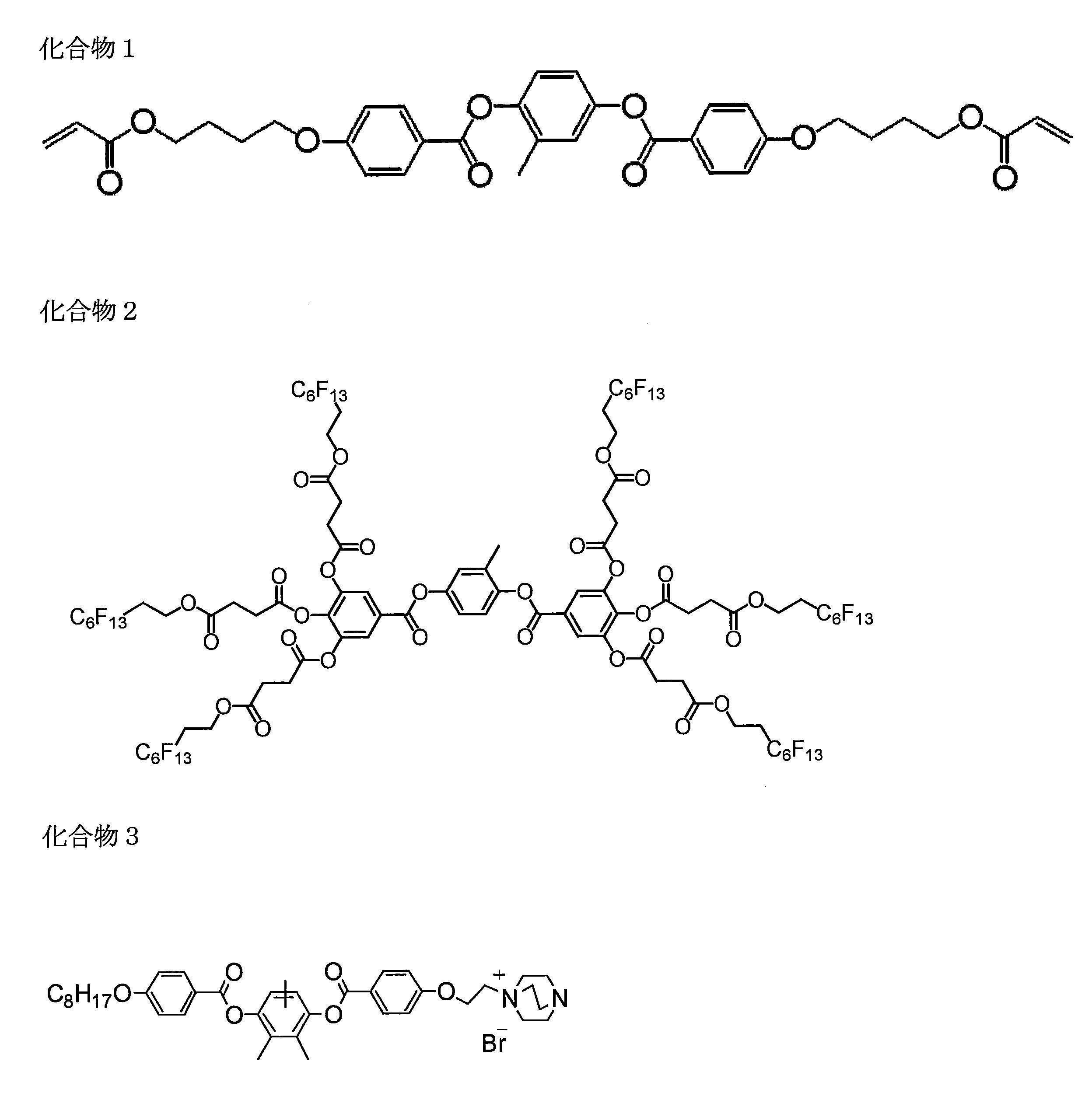
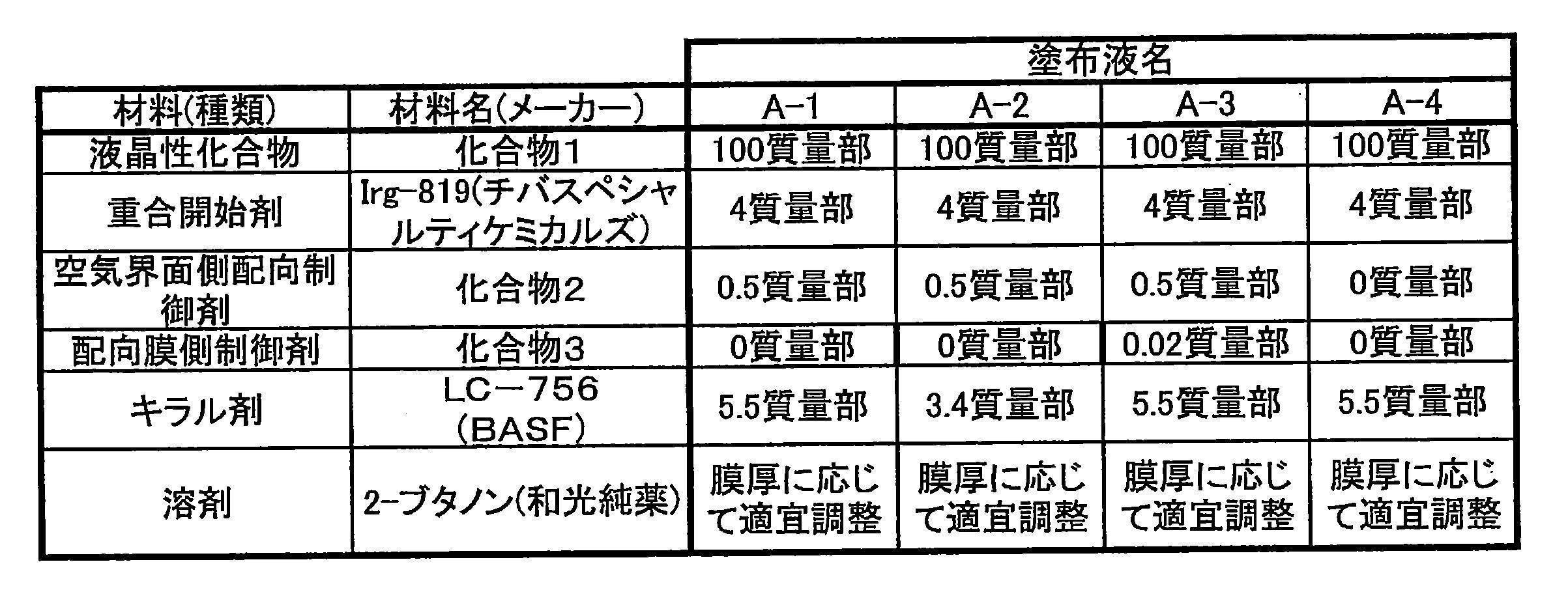
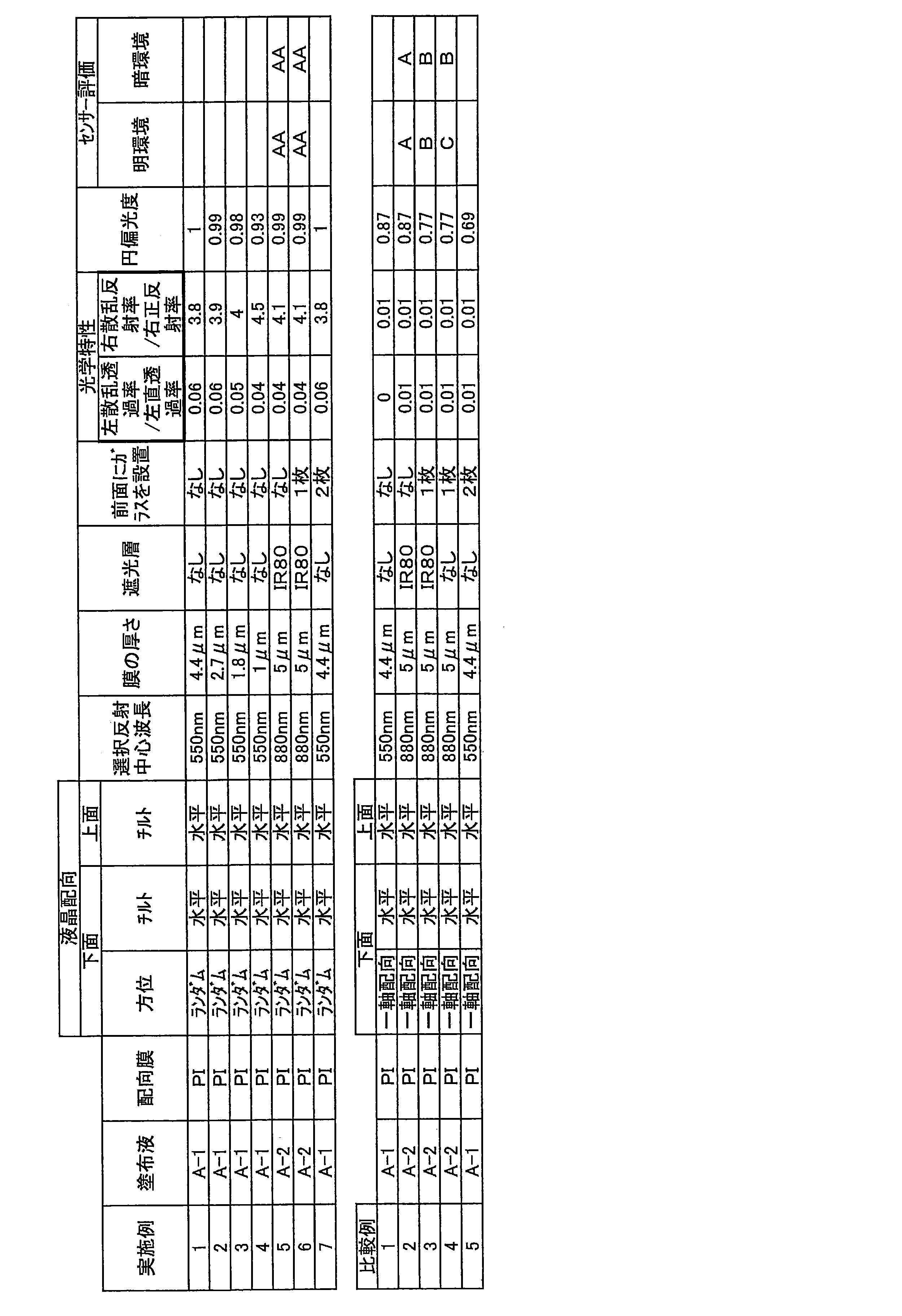
液晶を配向させるため、富士フイルム株式会社製PETにラビング処理を施し、処理面に表3に示す塗布液A-1を乾燥後の乾膜の厚みが5μmになるように室温にてワイヤーバーを用いて塗布した。塗布層を室温にて30秒間乾燥させた後、85℃の雰囲気で2分間加熱し、その後30℃でフュージョン製Dバルブ(ランプ90mW/cm)にて出力60%で6~12秒間UV照射し液晶層を得た。配向欠陥を持たない液晶層上に液晶層を形成すると、同様に配向欠陥を持たない液晶層となるため、この液晶層上に表3に示す塗布液A-2を乾燥後の乾膜の厚みが5μmになるように室温にて塗布し、その後上記と同様に乾燥、加熱、UV照射を行い、2層目の液晶層を形成して、非反射光散乱性円偏光分離層を得た。この非反射光散乱性円偏光分離層は配向欠陥を持たないことを偏光顕微鏡で確認した。その後、非反射光散乱性円偏光分離層の支持体となっていた富士フイルム株式会社製PETを剥離し、比較例11の円偏光フィルターを得た。
富士フイルム株式会社製PET面に、表4に示す塗布液Bを乾燥後の乾膜の厚みが8μmになるように室温にてワイヤーバーを用いて塗布した。塗布層を室温にて30秒間乾燥させた後、85℃の雰囲気で2分間加熱し、その後30℃でフュージョン製Dバルブ(ランプ90mW/cm)にて出力60%で6~12秒間UV照射しアクリル層を得た。このアクリル層上にラビング処理を施さずに表3に示す塗布液A-1を乾燥後の乾膜の厚みが5μmになるように室温にて塗布し、その後上記と同様に乾燥、加熱、UV照射を行い、液晶層を得た。配向欠陥を有する液晶層上に液晶層を形成すると、同様に配向欠陥を有する液晶層となるため、この液晶層上に表3に示す塗布液A-2を乾燥後の乾膜の厚みが5μmになるように室温にて塗布し、その後上記と同様に乾燥、加熱、UV照射を行い、2層目の液晶層を形成し、反射光散乱性円偏光分離層を得た。この反射光散乱性円偏光分離層は配向欠陥を持つことを偏光顕微鏡で確認した。
上記で作製した反射光散乱性円偏光分離層の液晶層側の面に、DIC株式会社製UV硬化型接着剤Exp.U12034-6を、乾燥後の乾膜の厚みが5μmになるように室温にてワイヤーバーを用いて塗布した。この塗布面と比較例11で作製した非反射光散乱性円偏光分離層の液晶層側の面とを気泡が入らないように貼りあわせ、その後30℃でフュージョン製Dバルブ(ランプ90mW/cm)にて出力60%で6~12秒間UV照射した。その後、反射光散乱性円偏光分離層、非反射光散乱性円偏光分離層の支持体となっていた富士フイルム株式会社製PETを剥離し、実施例11の円偏光フィルターを得た。
富士フイルム株式会社製PET面に、表4に示す塗布液Bを乾燥後の乾膜の厚みが8μmになるように室温にてワイヤーバーを用いて塗布した。塗布層を室温にて30秒間乾燥させた後、85℃の雰囲気で2分間加熱し、その後30℃でフュージョン製Dバルブ(ランプ90mW/cm)にて出力60%で6~12秒間UV照射しアクリル層を得た。このアクリル層上にラビング処理を施さずに表3に示す塗布液A-1を乾燥後の乾膜の厚みが4.5μmになるように室温にて塗布し、その後上記と同様に乾燥、加熱、UV照射を行い、液晶層を得た。この液晶層上に表に表3に示す塗布液A-2を乾燥後の乾膜の厚みが4.5μmになるように室温にて塗布し、その後上記と同様に乾燥、加熱、UV照射を行い、2層目の液晶層を形成して、反射光散乱性円偏光分離層を得た。
上記で作製した反射光散乱性円偏光分離層を比較例11で作製した非反射光散乱性円偏光分離層と同じ非反射光散乱性円偏光分離層と実施例11と同様の方法で貼合し実施例12の円偏光フィルターを得た。
富士フイルム株式会社製PET面に、表4に示す塗布液Bを乾燥後の乾膜の厚みが8μmになるように室温にてワイヤーバーを用いて塗布した。塗布層を室温にて30秒間乾燥させた後、85℃の雰囲気で2分間加熱し、その後30℃でフュージョン製Dバルブ(ランプ90mW/cm)にて出力60%で6~12秒間UV照射しアクリル層を得た。このアクリル層上にラビング処理を施さずに表3に示す塗布液A-3を乾燥後の乾膜の厚みが5μmになるように室温にて塗布し、その後上記と同様に乾燥、加熱、UV照射を行い、液晶層を得た。この液晶層上に表3に示す塗布液A-4を乾燥後の乾膜の厚みが5μmになるように室温にて塗布し、その後上記と同様に乾燥、加熱、UV照射を行い、2層目の液晶層を形成して、反射光散乱性円偏光分離層を得た。
上記で作製した反射光散乱性円偏光分離層を比較例11で作製した非反射光散乱性円偏光分離層と同じ非反射光散乱性円偏光分離層と実施例11と同様の方法で貼合し比較例12の円偏光フィルターを得た。
比較例11で得られた非反射光散乱性円偏光分離層の液晶層側の面上に、表5に示す塗布液Cを乾燥後の乾膜の厚みが10μmになるように室温にてワイヤーバーを用いて塗布した。塗布層を室温にて30秒間乾燥させた後、85℃の雰囲気で2分間加熱し、その後30℃でフュージョン製Dバルブ(ランプ90mW/cm)にて出力60%で6~12秒間UV照射した。その後、非反射光散乱性円偏光分離層の支持体となっていた富士フイルム株式会社製PETを剥離し、比較例13の円偏光フィルターを得た。
富士フイルム株式会社製PET面に、表4に示す塗布液Bを乾燥後の乾膜の厚みが8μmになるように室温にてワイヤーバーを用いて塗布した。塗布層を室温にて30秒間乾燥させた後、85℃の雰囲気で2分間加熱し、その後30℃でフュージョン製Dバルブ(ランプ90mW/cm)にて出力60%で6~12秒間UV照射しアクリル層を得た。このアクリル層上にラビング処理を施さずに表3に示す塗布液A-5を乾燥後の乾膜の厚みが5μmになるように室温にて塗布し、その後上記と同様に乾燥、加熱、UV照射を行い、液晶層を得た。この液晶層上に表3に示す塗布液A-6を乾燥後の乾膜の厚みが5μmになるように室温にて塗布し、その後上記と同様に乾燥、加熱、UV照射を行い、2層目の液晶層を形成して、反射光散乱性円偏光分離層を得た。
上記で作製した反射光散乱性円偏光分離層を非反射光散乱性円偏光分離層と実施例11と同様の方法で貼合し実施例13の円偏光フィルターを得た。
ラビング処理を施した富士フイルム株式会社製PET上のラビング処理面に、表6に示す塗布液Dを、2000rpmの回転数でスピン塗布した。塗布層を室温にて30秒間乾燥させた後、85℃の雰囲気で2分間加熱し、その後30℃でフュージョン製Dバルブ(ランプ90mW/cm)にて出力60%で6~12秒間UV照射し位相差膜を形成した。
この位相差膜の位相差をAxometrix社のAxoScanを用いて、400nm~800nmの範囲で測定し、これらの値を用いて880nmにおける位相差を外挿法で求めたところ220nmの位相差であった。
この膜の位相差膜表面にDIC株式会社製UV硬化型接着剤Exp.U12034-6を、乾燥後の乾膜の厚みが5μmになるように室温にてワイヤーバーを用いて塗布した。液晶分子の配向軸が偏光板の吸収軸との面内でなす角度が45度になるようにエドモンド・オプティクス・ジャパン株式会社製の近赤外用直線偏光フィルムを貼り合せ、非反射光散乱性円偏光分離層を形成した。この非反射光散乱性円偏光分離層を上記のAxoScanを用いて、光入射側に偏光板が来るようにしてCircular Polarizanceを測定することによって、右円偏光板となっていることを確認した。
上記で作製した非反射光散乱性円偏光分離層の位相差膜の面上に実施例11で作製した反射光散乱性円偏光分離層と同様の反射光散乱性円偏光分離層を実施例11と同様の方法で貼合し実施例14の円偏光フィルターを得た。
実施例11で作製した反射光散乱性円偏光分離層の液晶層側の面上に、DIC株式会社製UV硬化型接着剤Exp.U12034-6を、乾燥後の乾膜の厚みが5μmになるように室温にてワイヤーバーを用いて塗布した。この塗布面と実施例11で作製した円偏光フィルターの非反射光散乱性円偏光分離層側の面とを気泡が入らないように貼りあわせ、その後30℃でフュージョン製Dバルブ(ランプ90mW/cm)にて出力60%で6~12秒間UV照射した。その後、反射光散乱性円偏光分離層の支持体となっていた富士フイルム株式会社製PETを剥離し、実施例15の円偏光フィルターを得た。
富士フイルム株式会社製IR80上に、DIC株式会社製UV硬化型接着剤Exp.U12034-6を、乾燥後の乾膜の厚みが5μmになるように室温にてワイヤーバーを用いて塗布した。この塗布面と実施例11で作製した円偏光フィルターの非反射光散乱性円偏光分離層側の面とを気泡が入らないように貼りあわせ、その後30℃でフュージョン製Dバルブ(ランプ90mW/cm)にて出力60%で6~12秒間UV照射し、フィルターを得た。その後、上記で作製したフィルターの富士フイルム株式会社製IR80側に、DIC株式会社製UV硬化型接着剤Exp.U12034-6を、乾燥後の乾膜の厚みが5μmになるように室温にてワイヤーバーを用いて塗布した。この塗布面と実施例11で作製した円偏光フィルターの非反射光散乱性円偏光分離層側の面とを気泡が入らないように貼りあわせ、その後30℃でフュージョン製Dバルブ(ランプ90mW/cm)にて出力60%で6~12秒間UV照射し、実施例16の円偏光フィルターを得た。
実施例16で作製した円偏光フィルター上の片面に、東亞合成株式会社製粘着剤アロンタックS-1511改を、乾燥後の乾膜の厚みが5μmになるように室温にてワイヤーバーを用いて塗布した。この塗布面と厚み0.3mmのアクリル板(日東樹脂工業株式会社製フラット板(品番001))を気泡が入らないように貼りあわせた。その後、もう片側の面上に、東亞合成株式会社製粘着剤アロンタックS-1511改を、乾燥後の乾膜の厚みが5μmになるように室温にてワイヤーバーを用いて塗布した。この塗布面と厚み0.4mmのアクリル板(日東樹脂工業株式会社製フラット板(品番001))を気泡が入らないように貼りあわせ、実施例17の円偏光フィルターを得た。
実施例11の反射光散乱性円偏光分離層のみ、非反射光散乱性円偏光分離層のみ、ならびに反射光散乱性円偏光分離層および非反射光散乱性円偏光分離層の積層体の円偏光透過率の測定を波長範囲700nm~1100nmにおいて行った。積層体においては非反射光散乱性円偏光分離層の面から測定光を入射した。測定は、JASCO製の分光光度計V-670に絶対反射率測定ユニットARV474S型を組み合わせたもの用いて、10nmの波長ステップで、光源側にエドモンド・オプティクス・ジャパン株式会社製の近赤外用直線偏光フィルム上にエドモンド・オプティクス・ジャパン株式会社製のアクロマティック波長板を、高速軸が偏光フィルムの吸収軸との面内でなす角度が45度になるように固定したものを設置して、直透過率を測定することによって行った。このとき、光源側から偏光フィルム、波長板の順になるように設置して測定した。このとき、光入射側に偏光板が来るようにしてCircular Polarizanceを測定することによって、右円偏光板(右円偏光を透過する偏光板)となっていることを確認した。なお、測定の際は、光軸に対し、円偏光分離フィルタが90°となるように位置を調整した。測定された円偏光透過率の結果を図3に示す。
作製した実施例11~17および比較例11~13の円偏光フィルターのそれぞれの反射光散乱性円偏光分離層、非円偏光分離層について、以下の項目で評価した。
(2-1) 直透過率、5°正反射率、散乱透過率、散乱反射率:
上述の実施例1~7、比較例1~5の円偏光フィルターの直透過率、5°正反射率、散乱透過率、散乱反射率の測定と同様に測定した。
作製した実施例11~17および比較例11~13の円偏光フィルター、鏡、光源(京セミ株式会社製KED880S4)、受光素子(新光電子株式会社製KS1364)を図4に示すように配置した。なお、フィルターは実施例11~14、比較例12、13については反射光散乱性円偏光分離層が鏡側となるように、実施例17については、0.4mmのアクリル板が鏡側となるように、配置した。(実施例15、16は裏表対称の積層構造のため、どちらの面が鏡側となってもよい。)
光源から中心波長880nmの非偏光をフィルターを介して鏡に対して照射し、鏡からの反射光が上記フィルターを透過した光を受光素子で感知して評価した。なお、測定の際は、フィルターを設置した状態で鏡位置で検知される光強度が最大になるように鏡の傾きおよび位置を調整した。フィルターが無い状態で測定した光強度の値を100として、フィルター設置して測定した値を補正して評価した。外乱防止のため、周囲の光を完全に遮断した状態で測定した。
評価基準は以下の通りである。結果を表7に示す。
A:0~5
B:6~15
C:16~100
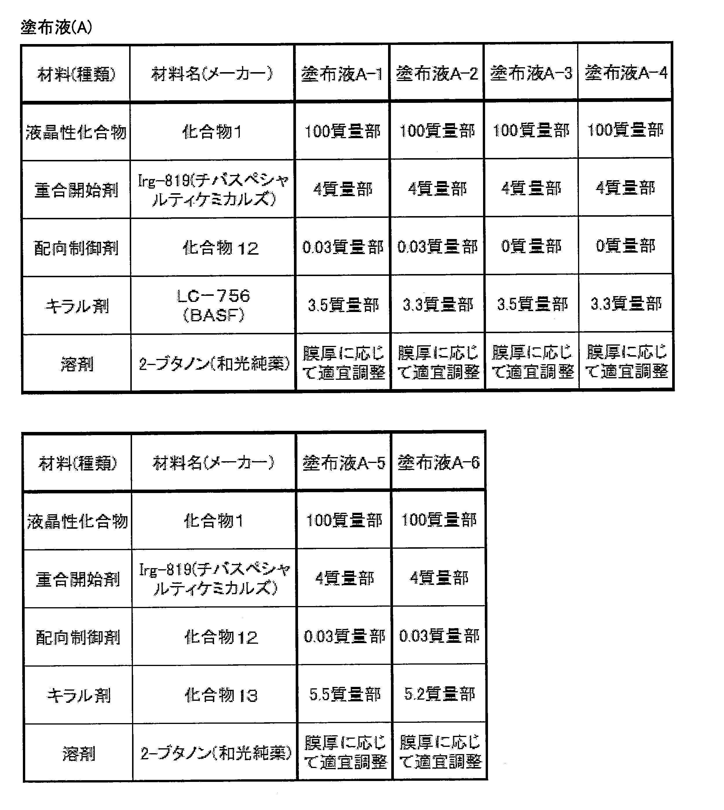
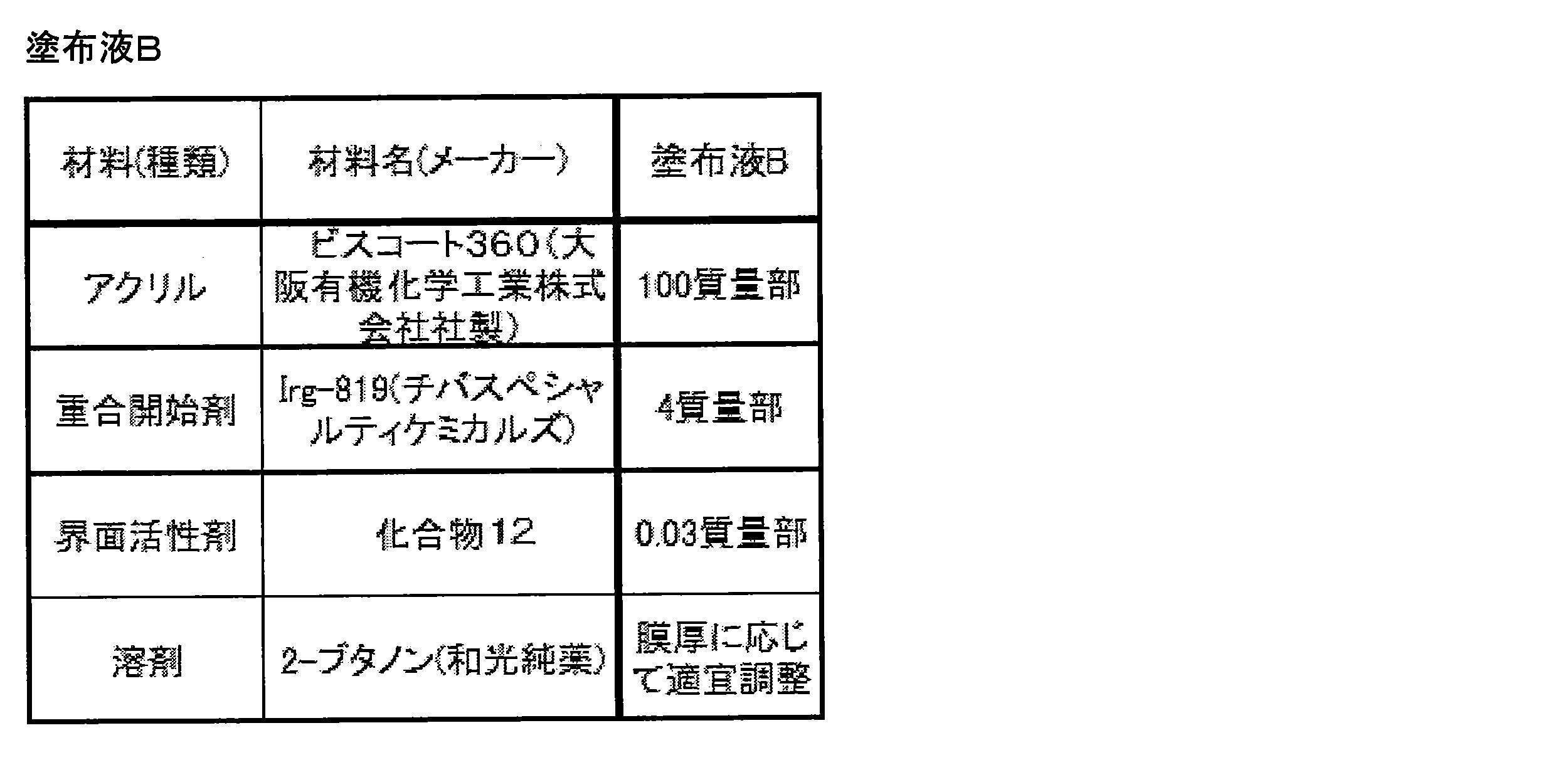

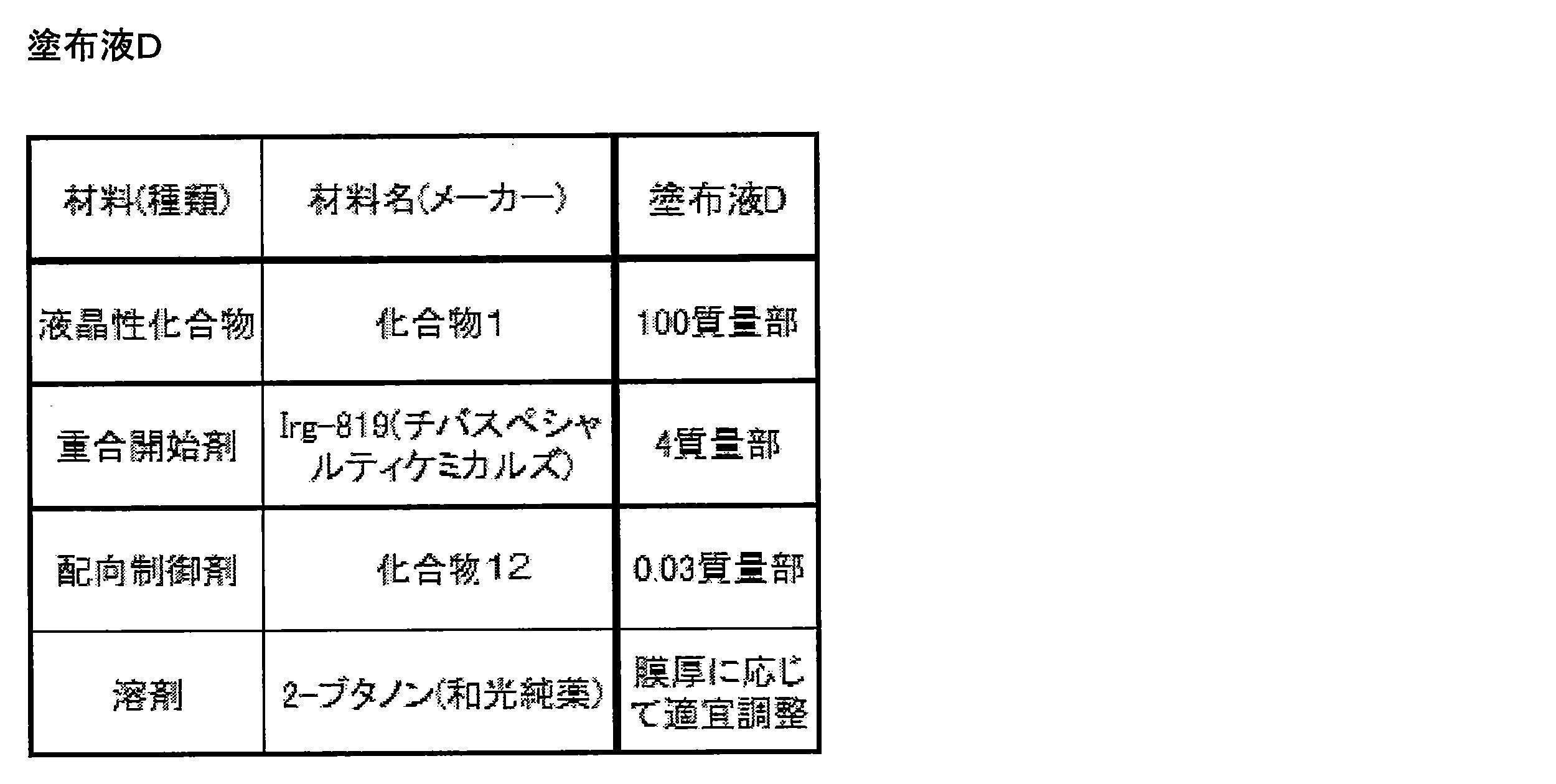


2 光源
3 受光素子(検出器)
4 対象物
5 透明ガラス
6 光遮断層
Claims (21)
- 特定の波長において右円偏光または左円偏光のいずれか一方のセンスの円偏光を選択的に透過させるための円偏光フィルターであって、
前記の特定の波長において右円偏光または左円偏光のいずれか一方のセンスの円偏光を選択的に透過させ、他方のセンスの円偏光を選択的に反射する円偏光分離層を含み、
前記円偏光分離層は反射光散乱性円偏光分離層を含み、
前記反射光散乱性円偏光分離層はコレステリック液晶相を固定した層からなり、かつ、
前記円偏光フィルターは、前記特定の波長において選択的に透過するセンスの円偏光をいずれか一方の面から入射したときの散乱透過率/直透過率より、前記特定の波長において他方のセンスの円偏光を前記面から入射したときの散乱反射率/正反射率が大きい、円偏光フィルター。 - 前記の反射光散乱性円偏光分離層は、内部にコレステリック液晶相の配向欠陥を有し、かつ
前記特定の波長の前記センスの円偏光の散乱透過率/直透過率より、他方のセンスの散乱反射率/正反射率が大きい、請求項1に記載の円偏光フィルター。 - 前記円偏光フィルターは、前記特定の波長において選択的に透過するセンスの円偏光をいずれか一方の面から入射したときの散乱透過率/直透過率が0.00以上0.10以下であり、前記特定の波長において他方のセンスの円偏光を前記面から入射したときの散乱反射率/正反射率が2.0以上7.5以下である請求項1または2に記載の円偏光フィルター。
- 前記反射光散乱性円偏光分離層は、前記特定の波長において選択的に透過するセンスの円偏光の散乱透過率/直透過率が0.00以上0.10以下であり、前記特定の波長において他方のセンスの散乱反射率/正反射率が2.0以上7.5以下である請求項1~3のいずれか一項に記載の円偏光フィルター。
- 前記反射光散乱性円偏光分離層は前記特定の波長の自然光で測定したヘイズ値が10より大きく55以下である、請求項1~4のいずれか一項に記載の円偏光フィルター。
- 前記反射光散乱性円偏光分離層は、少なくとも一方の表面側において前記コレステリック液晶相を形成する液晶化合物が水平配向している請求項1~5のいずれか一項に記載の円偏光フィルター。
- 前記反射光散乱性円偏光分離層がラビング処理を行わない膜表面に塗布した液晶化合物と空気界面配向剤とを含む組成物から形成された層である請求項1~6のいずれか一項に記載の円偏光フィルター。
- 前記円偏光分離層が非反射光散乱性円偏光分離層を含み、
前記非反射光散乱性円偏光分離層は前記の特定の波長において右円偏光または左円偏光のいずれか一方のセンスの円偏光を選択的に透過させ、他方のセンスの円偏光を選択的に反射させる層であり、かつ、反射光散乱性円偏光分離層および非反射光散乱性円偏光分離層が選択的に透過させる円偏光のセンスは同一であり、非反射光散乱性円偏光分離層は、前記特定の波長において選択的に透過するセンスの円偏光の散乱透過率/直透過率が0.00以上0.05以下であり、前記特定の波長において他方のセンスの円偏光の散乱反射率/正反射率が0.00以上0.05以下である請求項1~7のいずれか一項に記載の円偏光フィルター。 - 反射光散乱性円偏光分離層は前記特定の波長の自然光で測定したヘイズ値が10より大きく55以下であり、非反射光散乱性円偏光分離層は前記特定の波長の自然光で測定したヘイズ値が1.0以下である、請求項8に記載の円偏光フィルター。
- 非反射光散乱性円偏光分離層がコレステリック液晶相を固定した層からなる請求項8または9に記載の円偏光フィルター。
- 非反射光散乱性円偏光分離層が直線偏光分離層と前記の特定の波長においてλ/4位相差層として機能する層との積層体からなる請求項8または9に記載の円偏光フィルター。
- 前記の特定の波長が波長800nm~1500nmの範囲にある請求項1~11のいずれか一項に記載の円偏光フィルター。
- 前記の特定の波長を含まない波長域の少なくとも一部において光を遮断する光遮断層を含む請求項1~12のいずれか一項に記載の円偏光フィルター。
- 波長380~780nmの50nm幅以上の波長域において光を遮断する光遮断層を含む請求項12に記載の円偏光フィルター。
- 請求項1~14のいずれか一項に記載の円偏光フィルターと前記の特定の波長の光を照射できる光源とを含む光源装置。
- 請求項1~14のいずれか一項に記載の円偏光フィルターと前記の特定の波長の光を感知できる受光素子とを含むセンサー。
- 請求項1~14のいずれか一項に記載の円偏光フィルターと前記の特定の波長の光を照射できる光源と前記の特定の波長の光を感知できる受光素子とを含むセンサーシステム。
- 請求項8~10のいずれか一項に記載の円偏光フィルターと前記の特定の波長の光を照射できる光源とを含み、
前記光源、前記非反射光散乱性円偏光分離層、および前記反射光散乱性円偏光分離層がこの順で配置されている光源装置。 - 請求項8~10のいずれか一項に記載の円偏光フィルターと前記の特定の波長の光を感知できる受光素子とを含み、前記受光素子、前記非反射光散乱性円偏光分離層、および前記反射光散乱性円偏光分離層がこの順で配置されているセンサー。
- 請求項8~10のいずれか一項に記載の円偏光フィルターと前記の特定の波長域内の波長の光を照射できる光源と前記の特定の波長域内の波長の光を感知できる受光素子とを含むセンサーシステムであって、
前記光源、前記非反射光散乱性円偏光分離層、および前記反射光散乱性円偏光分離層がこの順で配置され、かつ
前記受光素子、前記非反射光散乱性円偏光分離層、および前記反射光散乱性円偏光分離層がこの順で配置されているセンサーシステム。 - 特定の波長において右円偏光または左円偏光のいずれか一方のセンスの円偏光を選択的に透過させるための円偏光フィルターの製造方法であって、
前記の特定の波長において右円偏光または左円偏光のいずれか一方のセンスの円偏光を選択的に透過させ、他方のセンスの円偏光を選択的に反射する円偏光分離層を含み、
前記円偏光分離層は反射光散乱性円偏光分離層を含み、
前記反射光散乱性円偏光分離層はコレステリック液晶相を固定した層からなり、
前記の反射光散乱性円偏光分離層の内部のコレステリック液晶相の配向欠陥を調整することにより、前記の反射光散乱性円偏光分離層が、前記特定の波長の前記センスの円偏光をいずれか一方の面から入射したときの散乱透過率/直透過率より、他方のセンスの円偏光を前記面から入射したときの散乱反射率/正反射率が大きくなるようにすることを含む製造方法。
Priority Applications (4)
| Application Number | Priority Date | Filing Date | Title |
|---|---|---|---|
| JP2015532888A JPWO2015025909A1 (ja) | 2013-08-21 | 2014-08-21 | 円偏光フィルターおよびその応用 |
| DE112014003848.2T DE112014003848T5 (de) | 2013-08-21 | 2014-08-21 | Zirkular polarisierender Filter und Anwendung hiervon |
| CN201480043942.6A CN105452915B (zh) | 2013-08-21 | 2014-08-21 | 圆偏振滤光器及其应用 |
| US15/014,640 US10139533B2 (en) | 2013-08-21 | 2016-02-03 | Circular polarizing filter and application thereof |
Applications Claiming Priority (4)
| Application Number | Priority Date | Filing Date | Title |
|---|---|---|---|
| JP2013-171483 | 2013-08-21 | ||
| JP2013171484 | 2013-08-21 | ||
| JP2013-171484 | 2013-08-21 | ||
| JP2013171483 | 2013-08-21 |
Related Child Applications (1)
| Application Number | Title | Priority Date | Filing Date |
|---|---|---|---|
| US15/014,640 Continuation US10139533B2 (en) | 2013-08-21 | 2016-02-03 | Circular polarizing filter and application thereof |
Publications (1)
| Publication Number | Publication Date |
|---|---|
| WO2015025909A1 true WO2015025909A1 (ja) | 2015-02-26 |
Family
ID=52483680
Family Applications (1)
| Application Number | Title | Priority Date | Filing Date |
|---|---|---|---|
| PCT/JP2014/071846 Ceased WO2015025909A1 (ja) | 2013-08-21 | 2014-08-21 | 円偏光フィルターおよびその応用 |
Country Status (5)
| Country | Link |
|---|---|
| US (1) | US10139533B2 (ja) |
| JP (1) | JPWO2015025909A1 (ja) |
| CN (1) | CN105452915B (ja) |
| DE (1) | DE112014003848T5 (ja) |
| WO (1) | WO2015025909A1 (ja) |
Cited By (5)
| Publication number | Priority date | Publication date | Assignee | Title |
|---|---|---|---|---|
| WO2016208327A1 (ja) * | 2015-06-24 | 2016-12-29 | 富士フイルム株式会社 | 車両用画像表示機能付きミラー |
| JP2018036314A (ja) * | 2016-08-29 | 2018-03-08 | 富士フイルム株式会社 | 偏光イメージセンサーおよび偏光イメージセンサーの製造方法 |
| JP2020052294A (ja) * | 2018-09-27 | 2020-04-02 | 大日本印刷株式会社 | 光学積層体及びこれを備える装置 |
| CN115165794A (zh) * | 2022-07-27 | 2022-10-11 | 南京工业职业技术大学 | 一种基于光学塔姆态光子自旋霍尔效应的超敏太赫兹液体传感器 |
| WO2025173647A1 (ja) * | 2024-02-16 | 2025-08-21 | 富士フイルム株式会社 | 偏光画像計測装置 |
Families Citing this family (11)
| Publication number | Priority date | Publication date | Assignee | Title |
|---|---|---|---|---|
| JP6502282B2 (ja) * | 2015-04-24 | 2019-04-17 | 富士フイルム株式会社 | 検知方法および検知システム |
| KR102659810B1 (ko) | 2015-09-11 | 2024-04-23 | 삼성디스플레이 주식회사 | 결정화도 측정 장치 및 그 측정 방법 |
| CN109219763B (zh) * | 2016-06-09 | 2021-03-05 | 3M创新有限公司 | 光学滤光器 |
| WO2018043678A1 (ja) * | 2016-09-01 | 2018-03-08 | 富士フイルム株式会社 | 加飾シート、液晶表示装置および自動車車内用内装 |
| WO2019013284A1 (ja) * | 2017-07-12 | 2019-01-17 | 富士フイルム株式会社 | 液晶組成物、反射層の製造方法、反射層、硬化物、光学異方体 |
| CN107703639A (zh) * | 2017-09-13 | 2018-02-16 | 维沃移动通信有限公司 | 一种光学式装置及移动终端 |
| WO2021020024A1 (ja) * | 2019-07-31 | 2021-02-04 | 日本ゼオン株式会社 | 表示媒体、表示物品及び表示セット |
| WO2021142638A1 (zh) * | 2020-01-15 | 2021-07-22 | 杭州芯格微电子有限公司 | 显示器下部的传感器 |
| CN114981693B (zh) * | 2020-01-31 | 2025-02-25 | 日本瑞翁株式会社 | 识别介质、物品以及识别介质的使用方法 |
| WO2022004496A1 (ja) * | 2020-07-01 | 2022-01-06 | 富士フイルム株式会社 | センサーおよびバンドパスフィルター |
| US12576631B1 (en) | 2023-01-11 | 2026-03-17 | SOLARCYCLE, Inc. | Delamination of used solar module |
Citations (4)
| Publication number | Priority date | Publication date | Assignee | Title |
|---|---|---|---|---|
| JP2007163894A (ja) * | 2005-12-14 | 2007-06-28 | Fujifilm Corp | 液晶表示装置 |
| JP2008083010A (ja) * | 2006-09-29 | 2008-04-10 | Honda Denshi Giken:Kk | 自動ドア開閉制御用反射型センサ |
| WO2012014552A1 (ja) * | 2010-07-26 | 2012-02-02 | 大日本印刷株式会社 | 電磁波反射フィルムおよびその製造方法 |
| JP2013036888A (ja) * | 2011-08-09 | 2013-02-21 | Mitsubishi Electric Corp | シリコン基板の検査装置、および検査方法 |
Family Cites Families (11)
| Publication number | Priority date | Publication date | Assignee | Title |
|---|---|---|---|---|
| US5150234A (en) * | 1988-08-08 | 1992-09-22 | Olympus Optical Co., Ltd. | Imaging apparatus having electrooptic devices comprising a variable focal length lens |
| USRE38500E1 (en) | 1997-10-09 | 2004-04-20 | Nitto Denko Corporation | Polarizer, optical element, lighting device and liquid crystal display |
| JP3591699B2 (ja) * | 1997-10-09 | 2004-11-24 | 日東電工株式会社 | 偏光素子、光学素子、照明装置及び液晶表示装置 |
| JP2003228038A (ja) * | 2002-02-01 | 2003-08-15 | Sony Corp | 調光装置及び撮像装置 |
| JPWO2003107048A1 (ja) * | 2002-06-17 | 2005-10-13 | 日本ゼオン株式会社 | 光学積層体、偏光光源装置および液晶表示装置 |
| DE10325610A1 (de) * | 2003-06-05 | 2004-12-30 | Consortium für elektrochemische Industrie GmbH | Polymerfilm mit helikaler Molekularstruktur |
| WO2007105721A1 (ja) * | 2006-03-13 | 2007-09-20 | Dai Nippon Printing Co., Ltd. | 光学拡散素子、投影スクリーン、意匠性部材及びセキュリティ媒体 |
| JP5647047B2 (ja) * | 2011-03-18 | 2014-12-24 | 日本発條株式会社 | 識別媒体 |
| JP5451672B2 (ja) * | 2011-03-25 | 2014-03-26 | 富士フイルム株式会社 | 光反射性フィルムの製造方法 |
| JP5718715B2 (ja) | 2011-04-22 | 2015-05-13 | 富士フイルム株式会社 | 植物成長制御用照明装置及び植物の成長制御方法 |
| JP2013109220A (ja) * | 2011-11-22 | 2013-06-06 | Nippon Zeon Co Ltd | 位相差フィルムを評価する評価方法 |
-
2014
- 2014-08-21 WO PCT/JP2014/071846 patent/WO2015025909A1/ja not_active Ceased
- 2014-08-21 DE DE112014003848.2T patent/DE112014003848T5/de not_active Ceased
- 2014-08-21 JP JP2015532888A patent/JPWO2015025909A1/ja active Pending
- 2014-08-21 CN CN201480043942.6A patent/CN105452915B/zh active Active
-
2016
- 2016-02-03 US US15/014,640 patent/US10139533B2/en active Active
Patent Citations (4)
| Publication number | Priority date | Publication date | Assignee | Title |
|---|---|---|---|---|
| JP2007163894A (ja) * | 2005-12-14 | 2007-06-28 | Fujifilm Corp | 液晶表示装置 |
| JP2008083010A (ja) * | 2006-09-29 | 2008-04-10 | Honda Denshi Giken:Kk | 自動ドア開閉制御用反射型センサ |
| WO2012014552A1 (ja) * | 2010-07-26 | 2012-02-02 | 大日本印刷株式会社 | 電磁波反射フィルムおよびその製造方法 |
| JP2013036888A (ja) * | 2011-08-09 | 2013-02-21 | Mitsubishi Electric Corp | シリコン基板の検査装置、および検査方法 |
Cited By (10)
| Publication number | Priority date | Publication date | Assignee | Title |
|---|---|---|---|---|
| WO2016208327A1 (ja) * | 2015-06-24 | 2016-12-29 | 富士フイルム株式会社 | 車両用画像表示機能付きミラー |
| JP2017007565A (ja) * | 2015-06-24 | 2017-01-12 | 富士フイルム株式会社 | 車両用の画像表示機能付きミラー |
| CN107683224A (zh) * | 2015-06-24 | 2018-02-09 | 富士胶片株式会社 | 车辆用带图像显示功能的反射镜 |
| US10501017B2 (en) | 2015-06-24 | 2019-12-10 | Fujifilm Corporation | Vehicle mirror with image display function |
| CN107683224B (zh) * | 2015-06-24 | 2020-06-05 | 富士胶片株式会社 | 车辆用带图像显示功能的反射镜 |
| JP2018036314A (ja) * | 2016-08-29 | 2018-03-08 | 富士フイルム株式会社 | 偏光イメージセンサーおよび偏光イメージセンサーの製造方法 |
| JP2020052294A (ja) * | 2018-09-27 | 2020-04-02 | 大日本印刷株式会社 | 光学積層体及びこれを備える装置 |
| JP7379811B2 (ja) | 2018-09-27 | 2023-11-15 | 大日本印刷株式会社 | 光学積層体及びこれを備える装置 |
| CN115165794A (zh) * | 2022-07-27 | 2022-10-11 | 南京工业职业技术大学 | 一种基于光学塔姆态光子自旋霍尔效应的超敏太赫兹液体传感器 |
| WO2025173647A1 (ja) * | 2024-02-16 | 2025-08-21 | 富士フイルム株式会社 | 偏光画像計測装置 |
Also Published As
| Publication number | Publication date |
|---|---|
| DE112014003848T5 (de) | 2016-05-19 |
| CN105452915A (zh) | 2016-03-30 |
| US20160154156A1 (en) | 2016-06-02 |
| US10139533B2 (en) | 2018-11-27 |
| CN105452915B (zh) | 2018-09-28 |
| JPWO2015025909A1 (ja) | 2017-03-02 |
Similar Documents
| Publication | Publication Date | Title |
|---|---|---|
| WO2015025909A1 (ja) | 円偏光フィルターおよびその応用 | |
| JP6166977B2 (ja) | 円偏光フィルターおよびその応用 | |
| JP6132678B2 (ja) | 偏光フィルターおよびその応用 | |
| JP6254768B2 (ja) | 光を利用した検知システムおよび検知方法 | |
| JP6471162B2 (ja) | 検知システムおよび検知方法 | |
| WO2014181799A1 (ja) | 円偏光分離フィルム、円偏光分離フィルムの製造方法、赤外線センサー、ならびに光を利用した検知システムおよび検知方法 | |
| KR101944227B1 (ko) | 투영상 표시용 하프 미러 및 그 제조 방법, 그리고 투영상 표시 시스템 | |
| US9874669B2 (en) | Reflection film, optical member, and display | |
| KR20160035070A (ko) | 응력 표시 부재 및 응력 표시 부재를 이용한 스트레인 측정 방법 | |
| JP2016004487A (ja) | 光学的パターン読み取り方法、光学的パターン読み取りシステム、光学的パターン読み取り装置、および光学的パターンを含む光学部材 | |
| JP6193471B2 (ja) | 投映像表示用部材および投映像表示用部材を含む投映システム | |
| US10598588B2 (en) | Sensing method and sensing system | |
| JP6254770B2 (ja) | 円偏光分離フィルムおよび円偏光分離フィルムの製造方法、ならびに赤外線センサー | |
| JP6254769B2 (ja) | 円偏光分離フィルムおよび円偏光分離フィルムの製造方法、ならびに赤外線センサー | |
| WO2016171218A1 (ja) | 検知方法および検知システム | |
| JP2017227924A (ja) | 円偏光分離フィルムおよび円偏光分離フィルムの製造方法、ならびに赤外線センサー | |
| JP6588517B2 (ja) | 円偏光分離フィルムおよび円偏光分離フィルムの製造方法、ならびに赤外線センサー | |
| WO2019230890A1 (ja) | 信号検出システム |
Legal Events
| Date | Code | Title | Description |
|---|---|---|---|
| WWE | Wipo information: entry into national phase |
Ref document number: 201480043942.6 Country of ref document: CN |
|
| 121 | Ep: the epo has been informed by wipo that ep was designated in this application |
Ref document number: 14837401 Country of ref document: EP Kind code of ref document: A1 |
|
| DPE1 | Request for preliminary examination filed after expiration of 19th month from priority date (pct application filed from 20040101) | ||
| ENP | Entry into the national phase |
Ref document number: 2015532888 Country of ref document: JP Kind code of ref document: A |
|
| WWE | Wipo information: entry into national phase |
Ref document number: 112014003848 Country of ref document: DE Ref document number: 1120140038482 Country of ref document: DE |
|
| 122 | Ep: pct application non-entry in european phase |
Ref document number: 14837401 Country of ref document: EP Kind code of ref document: A1 |