WO2015022741A1 - 半導体装置 - Google Patents
半導体装置 Download PDFInfo
- Publication number
- WO2015022741A1 WO2015022741A1 PCT/JP2013/071954 JP2013071954W WO2015022741A1 WO 2015022741 A1 WO2015022741 A1 WO 2015022741A1 JP 2013071954 W JP2013071954 W JP 2013071954W WO 2015022741 A1 WO2015022741 A1 WO 2015022741A1
- Authority
- WO
- WIPO (PCT)
- Prior art keywords
- data
- bit
- storage unit
- cell
- twin
- Prior art date
- Legal status (The legal status is an assumption and is not a legal conclusion. Google has not performed a legal analysis and makes no representation as to the accuracy of the status listed.)
- Ceased
Links
Images









Classifications
-
- G—PHYSICS
- G06—COMPUTING OR CALCULATING; COUNTING
- G06F—ELECTRIC DIGITAL DATA PROCESSING
- G06F12/00—Accessing, addressing or allocating within memory systems or architectures
- G06F12/14—Protection against unauthorised use of memory or access to memory
- G06F12/1408—Protection against unauthorised use of memory or access to memory by using cryptography
-
- G—PHYSICS
- G06—COMPUTING OR CALCULATING; COUNTING
- G06F—ELECTRIC DIGITAL DATA PROCESSING
- G06F21/00—Security arrangements for protecting computers, components thereof, programs or data against unauthorised activity
- G06F21/60—Protecting data
- G06F21/62—Protecting access to data via a platform, e.g. using keys or access control rules
- G06F21/6218—Protecting access to data via a platform, e.g. using keys or access control rules to a system of files or objects, e.g. local or distributed file system or database
-
- G—PHYSICS
- G06—COMPUTING OR CALCULATING; COUNTING
- G06F—ELECTRIC DIGITAL DATA PROCESSING
- G06F21/00—Security arrangements for protecting computers, components thereof, programs or data against unauthorised activity
- G06F21/70—Protecting specific internal or peripheral components, in which the protection of a component leads to protection of the entire computer
- G06F21/82—Protecting input, output or interconnection devices
- G06F21/85—Protecting input, output or interconnection devices interconnection devices, e.g. bus-connected or in-line devices
-
- G—PHYSICS
- G06—COMPUTING OR CALCULATING; COUNTING
- G06F—ELECTRIC DIGITAL DATA PROCESSING
- G06F3/00—Input arrangements for transferring data to be processed into a form capable of being handled by the computer; Output arrangements for transferring data from processing unit to output unit, e.g. interface arrangements
- G06F3/06—Digital input from, or digital output to, record carriers, e.g. RAID, emulated record carriers or networked record carriers
- G06F3/0601—Interfaces specially adapted for storage systems
- G06F3/0602—Interfaces specially adapted for storage systems specifically adapted to achieve a particular effect
- G06F3/062—Securing storage systems
- G06F3/0623—Securing storage systems in relation to content
-
- G—PHYSICS
- G06—COMPUTING OR CALCULATING; COUNTING
- G06F—ELECTRIC DIGITAL DATA PROCESSING
- G06F3/00—Input arrangements for transferring data to be processed into a form capable of being handled by the computer; Output arrangements for transferring data from processing unit to output unit, e.g. interface arrangements
- G06F3/06—Digital input from, or digital output to, record carriers, e.g. RAID, emulated record carriers or networked record carriers
- G06F3/0601—Interfaces specially adapted for storage systems
- G06F3/0628—Interfaces specially adapted for storage systems making use of a particular technique
- G06F3/0638—Organizing or formatting or addressing of data
-
- G—PHYSICS
- G06—COMPUTING OR CALCULATING; COUNTING
- G06F—ELECTRIC DIGITAL DATA PROCESSING
- G06F3/00—Input arrangements for transferring data to be processed into a form capable of being handled by the computer; Output arrangements for transferring data from processing unit to output unit, e.g. interface arrangements
- G06F3/06—Digital input from, or digital output to, record carriers, e.g. RAID, emulated record carriers or networked record carriers
- G06F3/0601—Interfaces specially adapted for storage systems
- G06F3/0668—Interfaces specially adapted for storage systems adopting a particular infrastructure
- G06F3/0671—In-line storage system
- G06F3/0683—Plurality of storage devices
-
- G—PHYSICS
- G11—INFORMATION STORAGE
- G11C—STATIC STORES
- G11C16/00—Erasable programmable read-only memories
- G11C16/02—Erasable programmable read-only memories electrically programmable
- G11C16/04—Erasable programmable read-only memories electrically programmable using variable threshold transistors, e.g. FAMOS
-
- G—PHYSICS
- G11—INFORMATION STORAGE
- G11C—STATIC STORES
- G11C16/00—Erasable programmable read-only memories
- G11C16/02—Erasable programmable read-only memories electrically programmable
- G11C16/04—Erasable programmable read-only memories electrically programmable using variable threshold transistors, e.g. FAMOS
- G11C16/0466—Erasable programmable read-only memories electrically programmable using variable threshold transistors, e.g. FAMOS comprising cells with charge storage in an insulating layer, e.g. metal-nitride-oxide-silicon [MNOS], silicon-oxide-nitride-oxide-silicon [SONOS]
- G11C16/0475—Erasable programmable read-only memories electrically programmable using variable threshold transistors, e.g. FAMOS comprising cells with charge storage in an insulating layer, e.g. metal-nitride-oxide-silicon [MNOS], silicon-oxide-nitride-oxide-silicon [SONOS] comprising two or more independent storage sites which store independent data
-
- G—PHYSICS
- G11—INFORMATION STORAGE
- G11C—STATIC STORES
- G11C16/00—Erasable programmable read-only memories
- G11C16/02—Erasable programmable read-only memories electrically programmable
- G11C16/06—Auxiliary circuits, e.g. for writing into memory
- G11C16/34—Determination of programming status, e.g. threshold voltage, overprogramming or underprogramming, retention
- G11C16/3418—Disturbance prevention or evaluation; Refreshing of disturbed memory data
- G11C16/3427—Circuits or methods to prevent or reduce disturbance of the state of a memory cell when neighbouring cells are read or written
-
- G—PHYSICS
- G11—INFORMATION STORAGE
- G11C—STATIC STORES
- G11C7/00—Arrangements for writing information into, or reading information out from, a digital store
- G11C7/10—Input/output [I/O] data interface arrangements, e.g. I/O data control circuits, I/O data buffers
- G11C7/1006—Data managing, e.g. manipulating data before writing or reading out, data bus switches or control circuits therefor
- G11C7/1012—Data reordering during input/output, e.g. crossbars, layers of multiplexers, shifting or rotating
-
- G—PHYSICS
- G11—INFORMATION STORAGE
- G11C—STATIC STORES
- G11C7/00—Arrangements for writing information into, or reading information out from, a digital store
- G11C7/10—Input/output [I/O] data interface arrangements, e.g. I/O data control circuits, I/O data buffers
- G11C7/1078—Data input circuits, e.g. write amplifiers, data input buffers, data input registers, data input level conversion circuits
- G11C7/1087—Data input latches
-
- G—PHYSICS
- G11—INFORMATION STORAGE
- G11C—STATIC STORES
- G11C16/00—Erasable programmable read-only memories
- G11C16/02—Erasable programmable read-only memories electrically programmable
- G11C16/06—Auxiliary circuits, e.g. for writing into memory
Definitions
- the present invention relates to a semiconductor device, for example, a semiconductor device including two nonvolatile memory cells that hold complementary data.
- Patent Document 1 a semiconductor device disclosed in Japanese Patent Application Laid-Open No. 2008-204507 (Patent Document 1) uses a scramble information generated by a random number generator to scramble write data and then writes to the data storage unit Is described. Since the scramble information is stored in the SRAM, which is a volatile memory, the scramble information is erased when the power is turned off so that the scramble information is erased even when the stored data remains in the data storage portion when the semiconductor device is turned off. The stored data cannot be read correctly. Thereby, the confidentiality of stored data can be improved.
- Patent Document 2 describes a non-volatile storage device that performs descrambling after writing data after being written and scrambled.
- the threshold voltages of the two cells are both reduced by erasing the twin cell data.
- the difference between the threshold voltages of the two cells in the write state before erasing the twin cell data may remain after erasing the twin cell data. Therefore, even though the twin cell data is erased, the write state before erasing the twin cell data is read, which may cause a security problem.
- Patent Document 1 has a problem that the stored data in the data storage unit is not read when the power is turned off.
- Patent Document 2 by storing a scrambled write data, a written flag that is a different bit pattern for each writing unit, and an error correction code, a power cutoff during writing, etc.
- the purpose is to detect anomalies, and the above-mentioned security problems cannot be solved.
- the scramble unit scrambles data to be written to the twin cell in the first storage unit using the scramble data.
- the writing unit writes the scrambled write data into the twin cells in the first storage unit.
- the writing unit writes the scrambled data into the memory cell in the second storage unit.
- the descrambling unit descrambles the data read from the first storage unit using the scramble data read from the second storage unit.
- FIG. 3 is a flowchart showing a procedure for erasing twin cell data from a memory array in the semiconductor device of the first embodiment. It is a figure showing the structure of the microcomputer of 3rd Embodiment. It is a figure showing the structure of a flash memory module.
- A) is a figure showing the example of the bias voltage given to a split gate type flash memory element.
- B) is a figure showing the example of the bias voltage given to the stacked gate type flash memory element using a hot carrier write system.
- (C) is a figure showing the example of the bias voltage given to the stacked gate type
- (A) is a diagram showing a state in which twin cell data stores “0”.
- (B) is a diagram showing a state in which twin cell data stores “1”.
- (C) is a diagram showing an initialized state of twin cell data.
- (A) is a diagram showing a sequence for erasing twin cell data “0”.
- (B) is a diagram showing a sequence for erasing twin cell data “1”. It is a figure showing the detailed circuit structure of the reading system of the twin cell data of 2nd Embodiment, a writing system, and an erasing system. It is a figure showing the main components which are concerned with writing and reading of the twin cell data in the semiconductor device of 3rd Embodiment.
- FIG. 1 It is a figure showing the structure of the expansion part engaged in writing and reading of the twin cell data in the semiconductor device of 4th Embodiment. It is a figure showing the main components engaged in writing and reading of the twin cell data in the semiconductor device of 5th Embodiment.
- (A) is a diagram showing a state in which a single cell stores single cell data “0”.
- (B) is a diagram showing a state in which a single cell stores single cell data “1”. It is a figure showing the main components engaged in writing and reading of the twin cell data in the semiconductor device of 6th Embodiment.
- (A) is a diagram showing a state in which three single cells store single cell data “0”.
- (B) is a diagram showing a state in which three single cells store single cell data “1”.
- FIG. 4 is a diagram illustrating a sense amplifier included in a read column selection circuit & sense amplifier. It is a figure showing the structure of the normal part and expansion part of 7th Embodiment. It is a figure showing the structure of the normal part of the modification of 7th Embodiment, and an expansion part. It is a figure showing 1 erase block structure of the memory array of 8th Embodiment. It is a figure showing the activation timing of the several source line in 8th Embodiment.
- FIG. 1 is a diagram illustrating the configuration of the semiconductor device according to the first embodiment.
- the semiconductor device 500 includes a first storage unit 502, a second storage unit 503, a scramble unit 501, a write unit 509, a write unit 511, and a descramble unit 504.
- the first storage unit 502 includes a twin cell 505.
- the twin cell 505 includes a memory cell 506 and a memory cell 507.
- the memory cell 506 and the memory cell 507 can be electrically rewritten.
- the twin cell 505 stores 1-bit data in a complementary manner depending on the difference in threshold voltage between the memory cell 506 and the memory cell 507.
- the second memory portion 503 includes an electrically rewritable memory cell 510.
- the data in the twin cell 505 in the first memory unit 502 is erased, the data in the memory cell 510 in the second memory unit 503 is also erased.
- the scramble unit 501 scrambles the data to be written in the twin cell 505 of the first storage unit 502 using the scramble data.
- the writing unit 509 writes the scrambled write data into the twin cell 505 in the first storage unit 502.
- the writing unit 511 writes scrambled data to the memory cell 510 in the second storage unit 503.
- the descrambling unit 504 descrambles the data read from the first storage unit 502 using the scramble data read from the second storage unit 503.
- FIG. 2 is a flowchart showing a procedure of a write process and a read process of write data to the first storage unit in the semiconductor device of the first embodiment.
- the semiconductor device receives a write request signal (step S101).
- the scramble unit 501 scrambles the data to be written to the twin cell 505 of the first storage unit 502 using the scramble data (step S102).
- the writing unit 509 writes the scrambled write data to the twin cell 505 in the first storage unit 502 (step S103).
- the writing unit 511 writes the scrambled data to the memory cell 510 in the second storage unit 503 (step S104).
- the semiconductor device receives a read request signal (step S105).
- the descrambling unit 504 performs descrambling processing on the data read from the first storage unit 502 using the scramble data read from the second storage unit 503 (step S106).
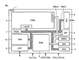
- FIG. 3 is a diagram illustrating the configuration of the microcomputer 1 according to the second embodiment.
- the microcomputer (MCU) 1 shown in FIG. 3 is formed on a single semiconductor chip such as single crystal silicon by, for example, complementary MOS integrated circuit manufacturing technology.
- the microcomputer 1 has a high-speed bus HBUS and a peripheral bus PBUS, although not particularly limited.
- the high-speed bus HBUS and the peripheral bus PBUS are not particularly limited, but each have a data bus, an address bus, and a control bus. By providing two buses, it is possible to reduce the load on the bus and to guarantee a high-speed access operation compared to the case where all circuits are commonly connected to the common bus.
- the high-speed bus HBUS includes a central processing unit (CPU) 2, a direct memory access controller (DMAC) 3, a bus interface control between the high-speed bus HBUS and the peripheral bus PBUS, or a bus that includes an instruction control unit and an execution unit to execute instructions.
- a bus interface circuit (BIF) 4 that performs bridge control is connected.
- RAM random access memory
- FMDL flash memory module
- the peripheral bus PBUS controls a flash sequencer (FSQC) 7 that performs command access control to the flash memory module (FMDL) 6, external input / output ports (PRT) 8 and 9, timer (TMR) 10, and microcomputer 1.
- FSQC flash sequencer
- FMDL flash memory module
- PRT external input / output ports
- TMR timer
- microcomputer 1 microcomputer 1.
- a clock pulse generator (CPG) 11 for generating an internal clock CLK is connected.
- the microcomputer 1 includes a clock terminal to which an oscillator is connected to XTAL / EXTAL or an external clock is supplied, an external hardware standby terminal STB for instructing a standby state, an external reset terminal RES for instructing a reset, an external power supply A terminal Vcc and an external ground terminal Vss are provided.
- the flash sequencer 7 as a logic circuit and the flash memory module 6 having an array configuration are designed using different CAD tools, and are therefore shown as separate circuit blocks for convenience.
- Configure flash memory The flash memory module 6 is connected to the high-speed bus HBUS via a read-only high-speed access port (HACSP).
- the CPU 2 or the DMAC 3 can read-access the flash memory module 6 from the high-speed bus HBUS via the high-speed access port.
- the CPU 2 or the DMAC 3 issues a command to the flash sequencer 7 via the peripheral bus PBUS via the bus interface 4 when performing write and initialization access to the flash memory module 6.
- the flash sequencer 7 initializes the flash memory module and controls the write operation from the peripheral bus PBUS through the low-speed access port (LACSP).
- LACSP low-speed access port
- FIG. 4 is a diagram showing the configuration of the flash memory module 6.
- the flash memory module 6 stores 1-bit information using two nonvolatile memory cells. That is, the memory array (MARY) 19 includes a plurality of two rewritable nonvolatile memory cells MCP and MCN as 1-bit twin cells. FIG. 4 representatively shows only one pair. In this specification, the memory cell MCP is called a positive cell, and the memory cell MCN is called a negative cell.
- the volatile memory cells MCP and MCN are, for example, split gate type flash memory elements exemplified in FIG.
- This memory element has a control gate CG and a memory gate MG disposed on a channel formation region between the source / drain regions via a gate insulating film.
- a charge trap region (SiN) such as silicon nitride is disposed between the memory gate MG and the gate insulating film.
- the source or drain region on the selection gate side is connected to the bit line BL, and the source or drain region on the memory gate MG side is connected to the source line SL.
- BL Hi ⁇ Z (high impedance state)
- CG Open
- MG ⁇ 10V
- Electrons are extracted from the charge trap region (SiN) to the well region (WELL) by the high electric field.
- This processing unit is a plurality of memory cells sharing the memory gate MG.
- BL 0V
- CG 0.9V
- MG 10V
- SL 6
- WELL 0V
- a write current is supplied from the source line SL to the bit line BL, thereby controlling the control gate.
- Hot electrons generated at the boundary between the CG and the memory gate MG are injected into the charge trap region (SiN). Since the electron injection is determined by whether or not a bit line current is passed, this process is controlled in units of bits.
- the memory element is not limited to the split gate type flash memory element, and may be a stacked gate type flash memory element exemplified in FIGS. 5B and 5C.
- This memory element is configured by stacking a floating gate FG and a control gate WL via a gate insulating film on a channel formation region between a source / drain region.
- the threshold voltage Vth is increased by the hot carrier writing method, and the threshold voltage Vth is decreased by the emission of electrons to the well region WELL.
- the threshold voltage Vth is increased by the FN tunnel writing method, and the threshold voltage Vth is decreased by the emission of electrons to the bit line BL.
- the voltage applied to the memory gate MG, control gate CG, source line SL, WELL, and bit line BL described above is generated and supplied by the power supply circuit (VPG) 31 under the control of the flash sequencer 7.
- the memory element is a split gate flash memory element.
- Information storage by one twin cell composed of nonvolatile memory cells MCP and MCN is performed by storing complementary data in nonvolatile memory cells MCP and MCN.
- each of the memory cells MCP and MCN has cell data “1” (low threshold voltage state; state in which the threshold voltage is smaller than the erase verify level) or cell data “0” (high threshold voltage state; the threshold voltage is in the erase verify state). State above the level).
- the twin cell data “0” is a state in which the positive cell MCP holds the cell data “0” and the negative cell MCN holds the cell data “1”.
- the twin cell data “1” is a state in which the positive cell MCP holds the cell data “1” and the negative cell MCN holds the cell data “0”.
- the state in which the positive cell MCP and the negative cell MCN of the twin cell both hold the cell data “1” is an initialized state, and the twin cell data becomes indefinite.
- the initialized state is also called a blank erase state.
- twin cell data erasure Further, changing from the initialized state to the twin cell data “1” holding state or the twin cell data “0” holding state is called normal writing.
- the cell data of both the positive cell MCP and the negative cell MCN is temporarily set to “0” (referred to as pre-write), and then the erase pulse is applied to both cell data. Processing to set “1” is performed.
- pre-write for both the positive cell MCP and the negative cell MCN, the applied voltage is made smaller than that during normal writing, or the writing pulse is weakened by shortening the period during which the writing pulse is applied. To do.
- the increase amount of the threshold voltage of the memory cell having the smaller threshold voltage is smaller than the increase amount of the threshold voltage Vth during normal writing.
- the purpose of performing the pre-write is to reduce variations in erasing stress between the positive cell MCP and the negative cell MCN and to suppress deterioration of the retention characteristics.
- a voltage smaller than the voltage during general normal write (increase Vth) shown in FIG. 5 is applied during prewrite.
- FIG. 7A shows a sequence for erasing twin cell data “0”.
- the erase of the twin cell data “0” when executed, both cells are initialized by the prewrite, but before the erase, Since the threshold voltage Vth of the positive cell MCP is larger than the threshold voltage Vth of the negative cell MCN, there is a possibility that this relationship is maintained even after erasing.
- the threshold voltage Vth between the positive cell MCP and the negative cell MCN is different regardless of the initialized state. Data “0” equal to “0” may be read.
- FIG. 7B shows a sequence for erasing twin cell data “1”.
- the erasure of the twin cell data “1” is executed, both cells are initialized by the pre-write, but before the erasure, Since the threshold voltage Vth of the negative cell MCN is larger than the threshold voltage Vth of the positive cell MCP, there is a possibility that this relationship is maintained even after erasing.
- the threshold voltage Vth between the positive cell MCP and the negative cell MCN is different regardless of the initialized state. Data “1” equal to “1” may be read.
- the embodiment of the present invention aims to solve such a possible problem.
- twin-cell memory cells MCP and MCN typically shown in FIG. 4, the memory gate MG is connected to a common memory gate selection line MGL, and the control gate CG is connected to a common word line WL. Actually, a large number of twin cells are arranged in a matrix and connected to the corresponding memory gate selection line MGL and word line WL in an array unit in the row direction. Memory cells MCP and MCN are connected to bit lines BLP and BLN in units of columns.
- the word line WL is selected by the first row decoder (RDEC1) 24.
- the memory gate selection line MGL is selected by the second row decoder (RDEC2) 25.
- the selection operation by the first row decoder 24 and the second row decoder 25 follows the address information supplied to the HACSP in the read access, and follows the address information supplied to the LACSP in the data write operation and the initialization operation.
- the write column selection circuit 51 selects a write column according to the decoding result of the column decoder (CDEC) 30, and writes write data sent from the input / output circuit (IOBUF) 29 interfaced to the data bus (PBUS_D) of the peripheral bus PBUS. Output to the scramble unit 35.
- the selection operation of the column decoder 30 follows address information supplied to the LACSP.
- the scramble unit 35 scrambles the write data sent from the write column selection circuit 51 and sends the scrambled write data to the write latch unit 36.
- the write latch unit 36 latches the scrambled write data and allows a write current to flow through either of the bit lines BLP and BLN of the selected write column, thereby causing the memory cell MCP of the selected write column to , MCN is written (that is, the threshold voltage Vth is increased).
- the verify unit 33 determines that the threshold voltage Vth of the memory cells MCP and MCN is at the write verify level according to the voltages of the bit lines BLP and BLN of the selected write column and the scrambled write data held in the write latch unit 36. To verify if it is greater than.
- the write verify result is supplied to the flash sequencer 7 through the peripheral data bus PBUS_D.
- the verify unit 33 executes erase verify. In the erase verify, it is verified whether or not the threshold voltage Vth of both the memory cells MCP and MCN constituting each twin cell in the erase target area is lower than the erase verify level.
- the erase verify result is supplied to the flash sequencer 7 through the peripheral data bus PBUS_D.
- bit line BLP connected to the memory cell MCP and the bit line BLN connected to the memory cell MCN are connected to the column selection & amplification unit 37.
- the column selection & amplification unit 37 selects a read column.
- the column selection & amplification unit 37 reads the twin cell data of the memory cells MCP and MCN of the selected read column by amplifying the voltage difference between the bit lines BLP and BLN of the selected read column.
- the descrambling unit 38 descrambles the read twin cell data output from the column selection & amplification unit 37 and outputs the data to the data bus HBUS_D of the high-speed bus HBUS via the output buffer (OBUF) 26.
- the power supply circuit (VPG) 31 generates various operating voltages necessary for reading, writing, and initialization.
- the timing generator (TMG) 32 generates an internal control signal that defines internal operation timing in accordance with an access strobe signal supplied from the CPU 2 or the like to the HACSP, an access command supplied from the FSQC 7 to the LACSP, or the like.
- the flash memory control unit includes a flash sequencer (FSQC) 7 and a timing generator (TMG) 32.
- FSQC flash sequencer
- TMG timing generator
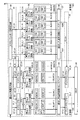
- FIG. 8 is a diagram illustrating main components involved in writing and reading twin cell data in the semiconductor device of the second embodiment.
- the semiconductor device of the second embodiment includes a normal part 100 and an extension part 101.
- the normal unit 100 includes a write column selection circuit 51, scramblers 61_1 to 61_N, inverters IVN_1 to IVN_N, write latch circuits 62P_1 to 62P_N, 62N_1 to 62N_N, a normal mat NMAT1, a read column selection circuit & sense amplifier 64. And descramblers 65_1 to 65_N.
- the extension unit 101 includes a scramble data generation circuit 52, inverters IVE_1 to IVE_N, write latch circuits 63P_1 to 63P_N, 63N_1 to 63N_N, an extension mat EMAT1, and a read column selection circuit & sense amplifier 66.
- the scramblers 61_1 to 61_N constitute the scramble unit 35 in FIG.
- the descramblers 65_1 to 65_N constitute the descramble unit 38 of FIG.
- the write latch circuits 62P_1 to 62P_N, 62N_1 to 62N_N, 63P_1 to 63P_N, 63N_1 to 63N_N constitute the write latch unit 36 of FIG.
- the read column selection circuit & sense amplifiers 64 and 66 constitute the column selection & amplification unit 37 of FIG.
- the scramble data generation circuit 52 generates N-bit scramble data S1 to SN. Each bit Si is sent to the write latch circuit 63P_i and also sent to the write latch circuit 63N_i via the inverter IVE_i.
- the scramble data generation circuit 52 outputs the same scramble data (S1 to SN) for the write data having the same row selected by the first row decoder (RDEC1) 24 and the second row decoder (RDEC2) 25. , Scramble data (S1 to SN) that are different from each other are output for write data that are different from each other.
- the scramble data generation circuit 52 outputs the scramble data (S1 to SN) to the write latch circuits 63P_1 to 63P_N and 63N_1 to 63N_N when the generated scramble data (S1 to SN) is not yet written in EMAT1. .
- the regular mat NMAT1 includes a plurality of twin cells MTC (i, j).
- i represents a column and is 1 to N.
- j represents a row and is 1 to L.
- Twin cell MTC (i, j) includes positive cell MCP (i, j) and negative cell MCN (i, j).
- Positive cell MCP (i, j) is connected to bit line BLNP_i.
- Negative cell MCN (i, j) is connected to bit line BLNN_i.
- the expansion mat EMAT1 includes a plurality of twin cells ETC (i, j).
- i represents a column and is 1 to N.
- j represents a row and is 1 to L.
- the twin cell ETC (i, j) includes a positive cell EMCP (i, j) and a negative cell EMCN (i, j).
- the positive cell EMCP (i, j) is connected to the bit line BLEP_i.
- the negative cell EMCN (i, j) is connected to the bit line BLEN_i.
- the write column selection circuit 51 selects a column in which data is written from the first column to the Nth column of the normal mat NMAT1.
- the write column selection circuit 51 outputs 1-bit write data sent from the input / output circuit (IOBUF) 29 to the scrambler 61_j corresponding to the selected column j.
- the scrambler 61_i scrambles the 1-bit write data with Si when the 1-bit write data D is sent from the write column selection circuit 51.
- the scrambled write data DSi are sent to the write latch circuit 62P_i and also sent to the write latch circuit 62N_i via the inverter IVN_i.
- Scramble processing means reversibly converting write data using scramble data.
- the descrambling process means obtaining original write data by converting the scrambled data using the scrambled data.
- exclusive OR of write data and scramble data is obtained by scramble processing
- original write data is obtained by exclusive OR of scrambled data and scramble data by descrambling processing.
- Vss the threshold voltage Vth of the memory cell MCP (i, k) in the selected row k increases, and cell data “0” is written.
- the write latch circuit 62N_i 1 to N
- the write latch circuit 62N_i 1 to N
- the bit line By connecting BLNN_i to the ground voltage Vss, a write current flows through the bit line BLNN_i.
- the threshold voltage Vth of the memory cell MCN (i, k) in the selected row k increases, and cell data “0” is written.
- the write current is prevented from flowing through the bit line BLNN_i.
- the threshold voltage Vth of the memory cell MCN (i, k) in the selected row k does not change.
- the read column selection circuit & sense amplifier 64 selects a column from which data is read from the first column to the Nth column of the normal mat NMAT1.
- the read column selection circuit & sense amplifier 64 amplifies the difference between the voltage of the bit line BLNP_j and the voltage of the bit line BLNN_j, reads the scrambled twin cell data, and Output to the tumbler 65_j.
- the row selected by the first row decoder (RDEC1) 24 and the second row decoder (RDEC2) 25 is k rows, the scrambled write data RDSj of the twin cell MTC (j, k) is read out.
- Si is “0”
- the write latch circuit 63P_i causes the write current to flow through the bit line BLEP_i by connecting the bit line BLEP_i to the ground voltage Vss while the write pulse WPLS is activated.
- the threshold voltage Vth of the memory cell EMCP (i, k) in the selected row k increases, and cell data “0” is written.
- / Si is “0”
- the write latch circuit 63N_i connects the bit line BLEN_i to the ground voltage Vss while the write pulse WPLS is activated so that the write current flows through the bit line BLEN_i. To do.
- the threshold voltage Vth of the memory cell EMCN (i, k) in the selected row k increases, and the cell data “0” is written.
- the read column selection circuit & sense amplifier 66 selects a column from which data is read from the first column to the Nth column of the expansion mat EMAT1.
- the read column selection circuit & sense amplifier 66 amplifies the difference between the voltage of the bit line BLEP_j and the voltage of the bit line BLEN_j, reads the scrambled data, and reads the scrambled data into the disk Output to the tumbler 65_j.
- the row selected by the first row decoder (RDEC1) 24 and the second row decoder (RDEC2) 25 is k rows, the scrambled data RSj of the twin cell ETC (j, k) is output.
- the read twin cell data RSj becomes equal to Sj.
- the read data RSj should originally be an indefinite value. May be equal to Sj as described with reference to FIG.
- the descrambling process is performed using the bit scrambled data RSi and the result is output to the output buffer (OBUF) 26.
- the scrambled write data when the scrambled write data is written to the regular mat and is not erased, the scrambled write data and the scrambled data are correctly read out.
- the write data can be normally restored by the descrambling process.
- the scrambled data When the scrambled write data is written to the regular mat and erased, the scrambled data is also erased from the extended mat. Even in this state, there is a possibility that both the scrambled write data before erasure and the scrambled data before erasure may be read, but the probability is low. Can be lowered.
- the bit selected by the write column selection circuit 51 and the twin cells in the row selected by the first row decoder (RDEC1) 24 and the second row decoder (RDEC2) 25 are scrambled by 1 bit.
- the write data is written, but the present invention is not limited to this.
- 1-bit scrambled write data is input to all the columns of the row selected by the first row decoder (RDEC1) 24 and the second row decoder (RDEC2) 25 when N-bit write data is input from the outside. May be written.
- the scrambler 61_i and the descrambler 65_i use the 1-bit data Si to scramble and descramble the write data.
- the scrambler 61_i and the descrambler 65_i may scramble and descramble the write data using a plurality of bits of the N-bit scramble data (S1 to SN).
- FIG. 9 is a diagram illustrating main components involved in writing and reading twin cell data in the semiconductor device of the third embodiment.
- the semiconductor device of FIG. 9 is different from the semiconductor device of the second embodiment of FIG. 8 as follows.
- 8 includes N scramblers 61_1 to 61_N and N descramblers 65_1 to 65_N, whereas the normal part 200 of the semiconductor device of FIG.
- the scrambler 71 and one descrambler 75 are provided.
- the scrambler 71 receives N-bit scramble data S1 to SN from the scramble data generation circuit 52.
- the scrambler 71 scrambles the 1-bit write data with Si.
- the scrambled write data DSi are sent to the write latch circuit 62P_i and also sent to the write latch circuit 62N_i via the inverter IVN_i.
- the descrambler 75 uses the 1-bit scrambled twin cell data RDSi output from the read column selection circuit & sense amplifier 64 and the 1-bit scramble data RSi output from the read column selection circuit & sense amplifier 66. The descrambling process is performed, and the result is output to the output buffer (OBUF) 26.
- the method of the descrambling process by the descrambler 75 cannot restore the write data DSi converted by using the scramble data Si in the scrambler 71 to the original write data D by using the same scramble data Si. must not.
- the scramble process and the descramble process for N columns of write data are performed by one scrambler 71 and one descrambler 75, so that the circuit scale is reduced. It can be made smaller than in the second embodiment.
- N-bit write data is input from the outside and is selected by the first row decoder (RDEC1) 24 and the second row decoder (RDEC2) 25.
- 1-bit scrambled write data may be written in each of all the columns in the row.
- FIG. 10 is a diagram illustrating a configuration of an extension unit involved in writing and reading of twin cell data in the semiconductor device of the fourth embodiment. Since the normal part is the same as that of the second embodiment, the description will not be repeated.
- the expansion unit 301 is different from the expansion unit 101 of the semiconductor device according to the second embodiment in FIG.
- the expansion unit 301 of FIG. 10 includes 6N write latch circuits 73P1_1 to 73P1_N, 73P2_1 to 73P2_N, 73P3_1 to 73P3_N, 73N1_1 to 73N1_N, 73N2_1 to 73N2_N, 73N3_1 to 73N3_N.
- the twin cell ETC (s, i, j) includes a positive cell EMCP (s, i, j) and a negative cell EMCN (s, i, j).
- the positive cell EMCP (s, i, j) is connected to the bit line BLEPs_i.
- the negative cell EMCN (s, i, j) is connected to the bit line BLENs_i.
- the scramble data generation circuit 52 generates N-bit scramble data S1 to SN. Each bit Si is sent to the write latch circuits 73P1_i, 73P2_i, 73P3_i, and is also sent to the write latch circuits 73N1_i, 73N2_i, 73N3_i via the inverter IVE_i.
- the write latch circuits 73P1_i, 73P2_i, 73P3_i receive 1-bit Si from the N-bit scrambled data S1 to SN from the scramble data generation circuit 52. When the Si is “0”, the write latch circuits 73P1_i, 73P2_i, and 73P3_i connect the bit lines BLEP1_i, BLEP2_i, and BLEP3_i to the ground voltage Vss during the period when the write pulse WPLS is activated. , BLEP2_i, BLEP3_i so that a write current flows.
- the threshold voltage Vth of the memory cells EMCP (1, i, k), EMCP (2, i, k), and EMCP (3, i, k) in the selected row k increases, and the cell data “0”. Is written.
- the write latch circuits 73P1_i, 73P2_i, and 73P3_i connect the bit lines BLEP1_i, BLEP2_i, and BLEP3_i to the power supply voltage VDD so that no write current flows through the bit lines BLEP1_i, BLEP2_i, and BLEP3_i.
- the threshold voltage Vth of the memory cells EMCP (1, i, k), EMCP (2, i, k), and EMCP (3, i, k) in the selected row k does not change.
- Write latch circuits 73N1_i, 73N2_i, 73N3_i receive 1-bit inverted value / Si of N-bit scrambled data S1 to SN from inverter IVE_i. When / Si is “0”, the write latch circuits 73N1_i, 73N2_i, and 73N3_i connect the bit lines BLEN1_i, BLEN2_i, and BLEN3_i to the ground voltage Vss while the write pulse WNLS is activated. A write current is caused to flow through BLEN1_i, BLEN2_i, and BLEN3_i.
- the threshold voltage Vth of the memory cells EMCN (1, i, k), EMCN (2, i, k), EMCN (3, i, k) of the selected row k increases, and the cell data “0” Is written.
- the write latch circuits 73N1_i, 73N2_i, and 73N3_i connect the bit lines BLEN1_i, BLEN2_i, and BLEN3_i to the power supply voltage VDD, whereby a write current flows through the bit lines BLEN1_i, BLEN2_i, and BLEN3_i. Do not.
- the threshold voltage Vth of the memory cells EMCN (1, i, k), EMCN (2, i, k), EMCN (3, i, k) in the selected row k does not change.
- the read column selection circuit & sense amplifier 66 selects a column from which data is read from the first column to the Nth column of the expansion mat EMAT2.
- the read column selection circuit & sense amplifier 66 amplifies the difference between the voltage of the bit line BLEP1_j and the voltage of the bit line BLEN1_j, reads the scrambled data, and outputs it to the determination circuit 77.
- the read column selection circuit & sense amplifier 66 amplifies the difference between the voltage of the bit line BLEP2_j and the voltage of the bit line BLEN2_j, reads the scrambled data, and outputs it to the determination circuit 77.
- the read column selection circuit & sense amplifier 66 amplifies the difference between the voltage of the bit line BLEP3_j and the voltage of the bit line BLEN3_j, reads the scrambled data, and outputs it to the determination circuit 77.
- the first scrambled data RSj1, twin cell ETC ( 2, j, k) second scrambled data RSj2 and third cell ETC (3, j, k) third scrambled data RSj3 are read out.
- the twin cell ETC (1, j, k), ETC (2, j, k), ETC (3, j, k), the twin cell ETC (1, j, k), ETC ( 2, j, k) and ETC (3, j, k) are not erased, the read data RSj1, RSj2, and RSj3 are equal to Sj.
- the twin cells ETC (1, j, k), ETC (2, j, k), ETC (3, j, k) are erased
- the twin cells ETC (1, j, k), ETC (2 , J, k) when data is read from ETC (3, j, k), the read data RSj1, RSj2, and RSj3 should originally be indefinite values, but FIG. 7 is used. As described above, it may be equal to Sj.
- the determination circuit 77 When the values of the first scramble data RSi1, the second scramble data RSi2, and the third scramble data RSi3 are all the same, the determination circuit 77 outputs the same value as the scramble data RSi that has been read.
- the determination circuit 77 is “0” when two of the first scrambled data RSi1, the second scrambled data RSi2, and the third scrambled data RSi3 are “1” and the rest are “0”. Is output as scrambled data RSi.
- the determination circuit 77 is “1” when two of the first scrambled data RSi1, the second scrambled data RSi2, and the third scrambled data RSi3 are “0” and the rest are “1”. Is output as scrambled data RSi.
- the scrambled data is written to the three twin cells of the expansion mat, and the scrambled data is determined based on the data values read from the three twin cells at the time of reading. The probability that the previous scrambled data is read can be reduced.
- FIG. 11 is a diagram illustrating main components involved in writing and reading twin cell data in the semiconductor device of the fifth embodiment.
- the semiconductor device of FIG. 11 is different from the semiconductor device of the second embodiment of FIG. 8 as follows.
- the semiconductor device in FIG. 8 includes 2N write latch circuits 63P_1 to 63P_N and 63N_1 to 63N_N, whereas the extension unit 401 in FIG. 11 includes N write latch circuits 83_1 to 83_N.
- the single cell EMC (i, j) is connected to the bit line BLE_i.
- the single cell data “0” is a state in which the memory cell MC holds the cell data “0” (high threshold voltage state; the threshold voltage is equal to or higher than the erase verify level).
- the single cell data “1” is a state in which the memory cell MC holds the cell data “1” (low threshold voltage state; the threshold voltage is smaller than the erase verify level).
- the scramble data generation circuit 52 generates N-bit scramble data S1 to SN. Each bit Si is sent to the write latch circuit 83_i.
- Si is “0”
- the write latch circuit 83_i connects the bit line BLE_i to the ground voltage Vss during a period in which the write pulse WPLS is activated so that a write current flows through the bit line BLE_i. .
- the threshold voltage Vth of the single cell EMC (i, k) in the selected row k increases, and the cell data “0” is written.
- the write latch circuit 83 — i prevents the write current from flowing through the bit line BLE_i by connecting the bit line BLE_i to the power supply voltage VDD.
- the threshold voltage Vth of the single cell EMC (i, k) in the selected row k does not change.
- the read column selection circuit & sense amplifier 86 selects a column from which data is read from the first column to the Nth column of the expansion mat EMAT3.
- One input terminal of the sense amplifier of the read column selection circuit & sense amplifier 66 is connected to the bit line BLE_j when the selected column is j, and the other input terminal is connected to the constant current source circuit. This sense amplifier amplifies the voltage difference between the two input terminals, reads the scrambled data, and outputs it to the descrambler 65_j.
- the scrambled data RSj of the single cell EMC (j, k) is output. After the scrambled data Sj is written to the single cell EMC (j, k), when the data of the single cell EMC (j, k) is not erased, the read data RSj becomes equal to Sj. On the other hand, when data is read from single cell EMC (j, k) after data in single cell EMC (j, k) is erased, read data RSj has a fixed value “1”. .
- the scrambled write data when the scrambled write data is written to the regular mat and is not erased, the scrambled write data and the scrambled data are correctly read out.
- the write data can be normally restored by the descrambling process.
- the scrambled data When the scrambled write data is written to the regular mat and erased, the scrambled data is also erased from the extended mat. In this state, the scrambled write data before erasure may be read out, but the scrambled data before erasure is not read out (fixed value “1” is read out). It is possible to prevent the write data from being restored by the processing.
- FIG. 13 is a diagram illustrating main components involved in writing and reading of twin cell data in the semiconductor device of the sixth embodiment.
- the semiconductor device of FIG. 13 is different from the semiconductor device of the second embodiment of FIG. 8 as follows.
- the extension unit 501 of FIG. 13 includes 3N write latch circuits 93_1_1 to 93_1_N, 93_2_1 to 93_2_N, 93_3_1 to It is a point provided with 93_3_N.
- the single cell EMC (s, i, j) is connected to the bit line BLEs_i.
- the scramble data generation circuit 52 generates N-bit scramble data S1 to SN. Each bit Si is sent to the write latch circuits 93_1_i, 93_2_i, and 93_3_i.
- the write latch circuits 93_1_i, 93_2_i, and 93_3_i receive 1-bit Si among the N-bit scrambled data S1 to SN from the scramble data generation circuit 52.
- Si is “0”
- the write latch circuits 93_1_i, 93_2_i, and 93_3_i connect the bit lines BLE1_i, BLE2_i, and BLE3_i to the ground voltage Vss during the period when the write pulse WPLS is activated. , BLE2_i, BLE3_i so that a write current flows.
- the threshold voltage Vth of the memory cells EMC (1, i, k), EMC (2, i, k), and EMC (3, i, k) in the selected row k increases, and the cell data “0”. Is written.
- the write latch circuits 93_1_i, 93_2_i, and 93_3_i connect the bit lines BLE1_i, BLE2_i, and BLE3_i to the power supply voltage VDD so that no write current flows through the bit lines BLE1_i, BLE2_i, and BLE3_i.
- the threshold voltage Vth of the memory cell EMC (1, i, k), EMC (2, i, k), EMC (3, i, k) in the selected row k does not change.
- memory cells EMC (1, i, k), EMC (2, i, k), EMC (3, i, k) Is a state in which the cell data “0” (high threshold voltage state; state in which the threshold voltage is equal to or higher than the erase verify level) is held.
- FIG. 14B when Si to be stored is “1”, the memory cells EMC (1, i, k), EMC (2, i, k), EMC (3, i, k) Is a state in which the cell data “1” (low threshold voltage state; state in which the threshold voltage is smaller than the erase verify level) is held.
- the read column selection circuit & sense amplifier 96 selects a column from which data is read from the first column to the Nth column of the expansion mat EMAT4.
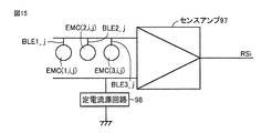
- FIG. 15 shows a sense amplifier 97 of the read column selection circuit & sense amplifier 96.
- the selected column is j
- one input terminal of the sense amplifier 97 is connected to the bit lines BLE1_j, BLE2_j, and BLE3_j, and the other input terminal is connected to the constant current source circuit 98.
- the sense amplifier 97 amplifies the voltage difference between the two input terminals, reads the scrambled data, and outputs the scrambled data to the descrambler 65_j.
- the constant current output from the constant current source circuit 98 is set to a value that considers the read margin.
- the read data RSj has a fixed value “1”.
- the scrambled write data when the scrambled write data is written to the regular mat and is not erased, the scrambled write data and the scrambled data are correctly read out.
- the write data can be normally restored by the descrambling process.
- the holding power of the scrambled data in the expansion mat can be enhanced as compared with the fifth embodiment.
- the scrambled data When the scrambled write data is written to the regular mat and erased, the scrambled data is also erased from the extended mat. In this state, the scrambled write data before erasure may be read out, but the scrambled data before erasure is not read out (fixed value “1” is read out). It is possible to prevent the write data from being restored by the processing.
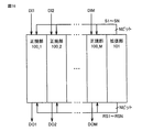
- FIG. 16 is a diagram illustrating the configuration of the normal part and the extension part of the seventh embodiment.
- the semiconductor device of this embodiment includes M normal parts 100 of the second embodiment shown in FIG. 8 (normal parts 100_1 to 100_N).
- the N-bit scramble data S1 to SN generated by the scramble data generation circuit 52 of the extension unit 101 is sent to the scramblers 61_1 to 61_N of the M normal units 100_1 to 100_M.
- the read N-bit scrambled data RS1 to RSN output from the read column selection circuit & sense amplifier 66 of the extension unit 101 are sent to the descramblers 65_1 to 65_N of the M normal units 100_1 to 100_M.
- the normal part 100_i corresponds to the data input pin DIi among the M data input pins DI1 to DIM, and corresponds to the data output pin DOi among the M data output pins DO1 to DOM.
- M normal parts 100_1 to 100_M execute simultaneous writing of M-bit write data from M data input pins DI1 to DIM, and M normal parts 100_1 to 100_M execute simultaneous reading, and M M-bit data read from the data output pins DO1 to DOM is output.
- N-bit scrambled data is applied to N ⁇ M columns of write data in the normal part, so that the area of the expansion mat can be made smaller than in the second embodiment. Can do.
- FIG. 17 is a diagram illustrating configurations of a normal part and an extension part according to a modification of the seventh embodiment.
- the semiconductor device of the present modification includes M normal parts 200 of the third embodiment in FIG. 9 (normal parts 200_1 to 200_M).
- the N-bit scramble data S1 to SN generated by the scramble data generation circuit 52 of the extension unit 101 is sent to the scramblers 71 of the M normal parts 200_1 to 200_M.
- the read N-bit scrambled data RS1 to RSN output from the read column selection circuit & sense amplifier 66 of the extension unit 101 are sent to the descrambler 75 of M normal parts 200_1 to 200_M.
- the normal part 200_i corresponds to the data input pin DIi in the M data input pins DI1 to DIM, and the data output in the M data output pins DO1 to DOM. Corresponds to pin DOi.
- M normal parts 200_1 to 200_M perform simultaneous writing of M-bit write data from M data input pins DI1 to DIM, and M normal parts 200_1 to 200_M perform simultaneous reading, and M M-bit data read from the data output pins DO1 to DOM is output.
- the N-bit scrambled data is applied to the N ⁇ M columns of write data of the normal part, so that the expansion mat area can be made smaller than in the third embodiment. it can.
- FIG. 18 is a diagram showing a 1-erasure block configuration of the memory array according to the eighth embodiment.
- An erase block consists of a regular mat and an extended mat.
- the regular mat of one erase block is divided into small blocks NMAT ⁇ 0> to NMAT ⁇ 31>.
- the extended mat of one erase block is divided into small blocks EMAT ⁇ 0> to EMAT ⁇ 31>.
- the small block NMAT ⁇ i> of the regular mat and the small block EMAT ⁇ i> of the expansion mat are arranged adjacent to each other.
- the scrambled data stored in the small block EMAT ⁇ i> of the extended mat may be used for the scramble process and the descramble process of the write data to the small block NMAT ⁇ i> of the regular mat.
- a part of the scrambled data stored in the small block EMAT ⁇ i> of the extended mat is used for the scramble process and the descramble process of the write data to the small block NMAT ⁇ i> of the regular mat
- One or more regular mat small blocks EMAT ⁇ j> (j ⁇ i) may be used for scramble processing and descramble processing of write data.
- the memory cells of the small block NMAT ⁇ i> of the normal mat and the small block EMAT ⁇ i> of the expansion mat are connected to the common source line SL ⁇ i>, and these memory cells are erased at the same timing.
- the source line SL ⁇ 0> is activated, and first, the memory cells of the small block NMAT ⁇ 0> of the normal mat and the small block EMAT ⁇ 0> of the expansion mat are erased. .
- the source line SL ⁇ 1> is activated, and the memory cells of the small block NMAT ⁇ 1> of the normal mat and the small block EMAT ⁇ 1> of the extended mat are erased.
- the source line SL ⁇ 31> is activated, and the memory cells of the normal mat small block NMAT ⁇ 31> and the extended mat small block EMAT ⁇ 31> are erased.
- the expansion mats are physically distributed and disposed, and therefore, only when a specific time-division erasure occurs when the expansion mats are physically concentrated. It is possible to avoid the problem that the number of bits increases or the extension mat needs to be erased by time division.
- the present invention is not limited to the above embodiment, and includes, for example, the following modifications.
- the write data is scrambled at the time of writing, and the read data is descrambled at the time of reading. It is not limited.
- a semiconductor device has both a normal write and read function and a write and descramble function with the scramble process, and can switch which function is executed. Good.
Landscapes
- Engineering & Computer Science (AREA)
- Theoretical Computer Science (AREA)
- Physics & Mathematics (AREA)
- General Engineering & Computer Science (AREA)
- General Physics & Mathematics (AREA)
- Computer Security & Cryptography (AREA)
- Computer Hardware Design (AREA)
- Human Computer Interaction (AREA)
- Microelectronics & Electronic Packaging (AREA)
- Software Systems (AREA)
- Databases & Information Systems (AREA)
- Health & Medical Sciences (AREA)
- Bioethics (AREA)
- General Health & Medical Sciences (AREA)
- Read Only Memory (AREA)
Abstract
Description
たとえば、特開2008-204507公報(特許文献1)の半導体装置は、乱数発生部により生成されたスクランブル情報を用いて、書込みデータに対しスクランブル処理を施してから、データ記憶部に書込みを行う方式が記載されている。スクランブル情報は、揮発性メモリであるSRAMに記憶されるので、半導体装置の電源オフ状態においてデータ記憶部に記憶データが残っていても、電源オフ時にスクランブル情報が消去されるためにデータ記憶部の記憶データを正しく読出すことができなくなる。これにより記憶データの秘匿性の向上を図ることができる。
[第1の実施形態]
図1は、第1の実施形態の半導体装置の構成を表わす図である。
第1の記憶部502は、ツインセル505を含む。ツインセル505は、メモリセル506と、メモリセル507とからなる。メモリセル506とメモリセル507は、電気的に書換え可能である。ツインセル505は、メモリセル506とメモリセル507の閾値電圧の相違によって相補的に1ビットのデータを記憶する。
第1の記憶部502内のツインセル505のデータが消去されるときには、第2の記憶部503内のメモリセル510のデータも消去される。
スクランブル部501は、第1の記憶部502のツインセル505に書込むデータをスクランブルデータを用いてスクランブル処理する(ステップS102)。
次に、ディスクランブル部504は、第2の記憶部503から読出されたスクラブルデータを用いて、第1の記憶部502から読出されたデータをディスクランブル処理する(ステップS106)。
本実施の形態の半導体装置は、マイクロコンピュータである。
(マイクロコンピュータ)
図3は、第2の実施形態のマイクロコンピュータ1の構成を表わす図である。
図4は、フラッシュメモリモジュール6の構成を表わす図である。
図7(a)に示すように、ツインセルデータ“0”の消去を実行する場合に、プレライトによって、両方のセルが共にセルデータ“1”を保持するイニシャライズ状態となるが、消去前はポジティブセルMCPの閾値電圧Vthの方がネガティブセルMCNの閾値電圧Vthよりも大きいため、消去後でもこの関係が維持される可能性が想定される。この関係が維持された状態で読出しを実施すると、イニシャライズ状態にも関わらずポジティブセルMCPとネガティブセルMCNの閾値電圧Vthに差があるために、不定値ではなく実質的に直前のツインセルデータ“0”と等しいデータ“0”を読出してしまう可能性がある。
図7(b)に示すように、ツインセルデータ“1”の消去を実行する場合に、プレライトによって、両方のセルが共にセルデータ“1”を保持するイニシャライズ状態となるが、消去前はネガティブセルMCNの閾値電圧Vthの方がポジティブセルMCPの閾値電圧Vthよりも大きいため、消去後でもこの関係が維持される可能性が想定される。この直前のツインセルデータ状態で読出しを実施すると、イニシャライズ状態にも関わらず、ポジティブセルMCPとネガティブセルMCNの閾値電圧Vthに差があるために、不定値ではなく実質的に直前のツインセルデータ“1”と等しいデータ“1”を読出してしまう可能性がある。
第2の実施形態では、書込み列選択回路51で選択された列、第1行デコーダ(RDEC1)24および第2行デコーダ(RDEC2)25によって選択された行のツインセルに1ビットのスクランブル処理された書込みデータが書込まれることとしたが、これに限定されるものではない。外部からNビットの書込みデータが入力され、第1行デコーダ(RDEC1)24および第2行デコーダ(RDEC2)25によって選択された行のすべての列のそれぞれに、1ビットのスクランブル処理された書込みデータが書込まれることとしてもよい。
[第3の実施形態]
図9は、第3の実施形態の半導体装置におけるツインセルデータの書込みおよび読出しに携わる主要な構成要素を表わす図である。
第3の実施形態においても、第2の実施形態の変形例と同様に、外部からNビットの書込みデータが入力され、第1行デコーダ(RDEC1)24および第2行デコーダ(RDEC2)25によって選択された行のすべての列のそれぞれに、1ビットのスクランブル処理された書込みデータが書込まれることとしてもよい。
[第4の実施形態]
図10は、第4の実施形態の半導体装置におけるツインセルデータの書込みおよび読出しに携わる拡張部の構成を表わす図である。正規部については、第2の実施形態と同様なので説明を繰り返さない。
図11は、第5の実施形態の半導体装置におけるツインセルデータの書込みおよび読出しに携わる主要な構成要素を表わす図である。
図13は、第6の実施形態の半導体装置におけるツインセルデータの書込みおよび読出しに携わる主要な構成要素を表わす図である。
図16は、第7の実施形態の正規部と拡張部の構成を表わす図である。
図17は、第7の実施形態の変形例の正規部と拡張部の構成を表わす図である。
図18は、第8の実施形態のメモリアレイの1消去ブロック構成を表わす図である。
本発明の実施の形態の半導体装置は、書込み時に書込みデータをスクランブル処理し、読出し時に読出しデータをディスクランブル処理することとしたが、本発明は、上記第1段階の処理に限定されるものではない。
Claims (12)
- 電気的に書換え可能で、閾値電圧の相違によって相補的に1ビットのデータを記憶するツインセルを含む第1の記憶部と、
電気的に書き換え可能なメモリセルを含む第2の記憶部と、
前記第1の記憶部内の前記ツインセルに書込むデータをスクランブルデータを用いてスクランブル処理するスクランブル部と、
前記第1の記憶部内の前記ツインセルにスクランブル処理後の書込みデータを書込む第1の書込み部と、
前記第2の記憶部内の前記メモリセルに前記スクランブルデータを書込む第2の書込み部と、
前記第2の記憶部から読出されたスクラブルデータを用いて、前記第1の記憶部から読出されたデータをディスクランブル処理するディスクランブル部とを備えた、半導体装置。 - 前記第2の記憶部は、2つメモリセルからなり、前記スクランブルデータの1ビットを記憶するツインセルを含む、請求項1記載の半導体装置。
- 前記第2の記憶部は、1つのメモリセルからなり、前記スクランブルデータの1ビットを記憶するシングルセルを含む、請求項1記載の半導体装置。
- 前記第2の記憶部は、1つのメモリセルからなり、前記スクランブルデータの1ビットを記憶する複数のシングルセルを含み、前記複数のシングルセルは、スクランブルデータの1ビットを重複して記憶し、
一方の入力端子が前記複数の単一のメモリセルと接続する複数のビット線に同時に接続され、他方の入力端子が定電流源回路と接続されるセンスアンプを備える、請求項1記載の半導体装置。 - 前記第2の記憶部は、2つメモリセルからなり、スクランブルデータの1ビットを記憶する複数のツインセルを含み、前記複数のツインセルは、スクランブルデータの1ビットを重複して記憶し、
前記複数のツインセルから読出された1ビットの値がすべて同一であるときには、前記同一の値を前記ディスクランブル部へ送り、前記複数のツインセルから読出された1ビットの値のうち他と異なるものがあるときには、頻度が少ない方の値を前記ディスクランブル部へ送る判定回路を備える、請求項1記載の半導体装置。 - 前記スクランブル部は、
前記第1の記憶部の列ごとに設けられる複数個のスクランブラーを含み、
前記スクランブラーは、対応の列のツインセルに対する1ビットの書込みデータを前記スクランブルデータを用いてスクランブル処理し、
前記ディスクランブル部は、
前記第1の記憶部の列ごとに設けられる複数個のディスクランブラーを含み、
前記ディスクランブラーは、対応の列のツインセルから読出された1ビットのデータを前記第2の記憶部から読出されたスクランブルデータ用いてディスクランブル処理する、請求項1記載の半導体装置。 - 前記スクランブルデータは、複数のビットで構成され、
前記スクランブラーは、対応の列のツインセルに対する1ビットの書込みデータを前記スクランブルデータを構成する複数ビットのうち前記列に対応する1ビットを用いてスクランブル処理し、
前記ディスクランブラーは、対応の列のツインセルから読出された1ビットのデータを前記スクランブルデータを構成する複数ビットのうち前記列に対応する1ビットを用いてディスクランブル処理する、請求項6記載の半導体装置。 - 前記スクランブル部は、
前記第1の記憶部の複数の列に共通に設けられるスクランブラーを含み、
前記スクランブラーは、前記ツインセルに対する1ビットの書込みデータを前記スクランブルデータを用いてスクランブル処理し、
前記ディスクランブル部は、
前記第1の記憶部の複数の列に共通に設けられるディィスクランブラーを含み、
前記ディスクランブラーは、前記ツインセルから読出された1ビットのデータを前記第2の記憶部から読出されたスクランブルデータ用いてディスクランブル処理する、請求項1記載の半導体装置。 - 前記スクランブルデータは、複数のビットで構成され、
前記スクランブラーは、ツインセルに対する1ビットの書込みデータを前記スクランブルデータを構成する複数ビットのうち前記ツインセルの列に対応する1ビットを用いてスクランブル処理し、
前記ディスクランブラーは、前記ツインセルから読出された1ビットのデータを前記スクランブルデータを構成する複数ビットのうち前記ツインセルの列に対応する1ビットを用いてディスクランブル処理する、請求項8記載の半導体装置。 - 複数組のデータ入力ピンおよびデータ出力ピンと、
データ入力ピンおよびデータ出力ピンの組ごとに、前記スクランブラーおよび前記ディスクランブラーを備え、
複数個の前記スクランブラーは、同一のスクランブルデータを用いてスクランブル処理し、複数個の前記ディスクランブラーは、同一のスクランブルデータを用いてディスクランブル処理する、請求項8記載の半導体装置。 - 前記第1の記憶部および前記第2の記憶部は、それぞれ同一の個数の小ブロックに分割され、
前記第1の記憶部の小ブロックおよび前記第2の記憶部の小ブロックの組は、同一のタイミングで消去される、請求項1記載の半導体装置。 - 前記第1の記憶部のデータが消去されるときには、前記第2の記憶部のデータも消去される、請求項1記載の半導体装置。
Priority Applications (4)
| Application Number | Priority Date | Filing Date | Title |
|---|---|---|---|
| JP2015531706A JP6185589B2 (ja) | 2013-08-15 | 2013-08-15 | 半導体装置および半導体装置におけるデータ秘匿方法 |
| US14/909,970 US10073982B2 (en) | 2013-08-15 | 2013-08-15 | Semiconductor device |
| PCT/JP2013/071954 WO2015022741A1 (ja) | 2013-08-15 | 2013-08-15 | 半導体装置 |
| US16/105,231 US10339335B2 (en) | 2013-08-15 | 2018-08-20 | Semiconductor device |
Applications Claiming Priority (1)
| Application Number | Priority Date | Filing Date | Title |
|---|---|---|---|
| PCT/JP2013/071954 WO2015022741A1 (ja) | 2013-08-15 | 2013-08-15 | 半導体装置 |
Related Child Applications (2)
| Application Number | Title | Priority Date | Filing Date |
|---|---|---|---|
| US14/909,970 A-371-Of-International US10073982B2 (en) | 2013-08-15 | 2013-08-15 | Semiconductor device |
| US16/105,231 Continuation US10339335B2 (en) | 2013-08-15 | 2018-08-20 | Semiconductor device |
Publications (1)
| Publication Number | Publication Date |
|---|---|
| WO2015022741A1 true WO2015022741A1 (ja) | 2015-02-19 |
Family
ID=52468142
Family Applications (1)
| Application Number | Title | Priority Date | Filing Date |
|---|---|---|---|
| PCT/JP2013/071954 Ceased WO2015022741A1 (ja) | 2013-08-15 | 2013-08-15 | 半導体装置 |
Country Status (3)
| Country | Link |
|---|---|
| US (2) | US10073982B2 (ja) |
| JP (1) | JP6185589B2 (ja) |
| WO (1) | WO2015022741A1 (ja) |
Cited By (1)
| Publication number | Priority date | Publication date | Assignee | Title |
|---|---|---|---|---|
| KR20180106982A (ko) * | 2017-03-21 | 2018-10-01 | 르네사스 일렉트로닉스 가부시키가이샤 | 스토리지 디바이스 및 스토리지 방법 |
Families Citing this family (6)
| Publication number | Priority date | Publication date | Assignee | Title |
|---|---|---|---|---|
| US10372948B2 (en) * | 2015-12-15 | 2019-08-06 | Taiwan Semiconductor Manufacturing Company Ltd. | Scrambling apparatus and method thereof |
| JP6181218B2 (ja) * | 2016-02-09 | 2017-08-16 | ウィンボンド エレクトロニクス コーポレーション | 半導体記憶装置 |
| KR102601216B1 (ko) * | 2016-09-29 | 2023-11-10 | 삼성전자주식회사 | 반도체 장치의 설계 방법 |
| JP6997595B2 (ja) * | 2017-11-09 | 2022-01-17 | ルネサスエレクトロニクス株式会社 | 半導体記憶装置、及び半導体記憶装置の制御方法 |
| JP2019179799A (ja) * | 2018-03-30 | 2019-10-17 | ルネサスエレクトロニクス株式会社 | 半導体記憶装置 |
| US11270763B2 (en) * | 2019-01-18 | 2022-03-08 | Silicon Storage Technology, Inc. | Neural network classifier using array of three-gate non-volatile memory cells |
Citations (5)
| Publication number | Priority date | Publication date | Assignee | Title |
|---|---|---|---|---|
| JP2008117510A (ja) * | 2006-10-11 | 2008-05-22 | Renesas Technology Corp | 半導体装置 |
| JP2008204507A (ja) * | 2007-02-16 | 2008-09-04 | Renesas Technology Corp | 半導体装置 |
| JP2009157841A (ja) * | 2007-12-27 | 2009-07-16 | Toshiba Corp | メモリシステム |
| JP2010512560A (ja) * | 2008-02-29 | 2010-04-22 | 株式会社東芝 | 情報処理装置及び不揮発性半導体メモリドライブ |
| JP2011508363A (ja) * | 2007-12-31 | 2011-03-10 | サンディスク コーポレイション | オンチップコピー操作適合データスクランブリングを提供するシステム、方法、およびメモリデバイス |
Family Cites Families (18)
| Publication number | Priority date | Publication date | Assignee | Title |
|---|---|---|---|---|
| JPS61181239A (ja) | 1985-02-06 | 1986-08-13 | Matsushita Electric Works Ltd | デ−タ送信機 |
| JP3638770B2 (ja) | 1997-12-05 | 2005-04-13 | 東京エレクトロンデバイス株式会社 | テスト機能を備える記憶装置 |
| US6385727B1 (en) * | 1998-09-25 | 2002-05-07 | Hughes Electronics Corporation | Apparatus for providing a secure processing environment |
| JP4079552B2 (ja) * | 1999-07-16 | 2008-04-23 | 富士通株式会社 | 不正コピーを防止した不揮発性半導体メモリ |
| CN100418032C (zh) | 2003-06-30 | 2008-09-10 | Nxp股份有限公司 | 密钥复制保护存储的数字自我擦除 |
| US7177183B2 (en) * | 2003-09-30 | 2007-02-13 | Sandisk 3D Llc | Multiple twin cell non-volatile memory array and logic block structure and method therefor |
| US20060232826A1 (en) * | 2005-04-13 | 2006-10-19 | Hagai Bar-El | Method, device, and system of selectively accessing data |
| US20080052446A1 (en) * | 2006-08-28 | 2008-02-28 | Sandisk Il Ltd. | Logical super block mapping for NAND flash memory |
| JP4498370B2 (ja) | 2007-02-14 | 2010-07-07 | 株式会社東芝 | データ書き込み方法 |
| US7876615B2 (en) * | 2007-11-14 | 2011-01-25 | Jonker Llc | Method of operating integrated circuit embedded with non-volatile programmable memory having variable coupling related application data |
| US8099544B2 (en) | 2008-02-29 | 2012-01-17 | Kabushiki Kaisha Toshiba | Information processing apparatus and nonvolatile semiconductor memory drive |
| US9123422B2 (en) * | 2012-07-02 | 2015-09-01 | Super Talent Technology, Corp. | Endurance and retention flash controller with programmable binary-levels-per-cell bits identifying pages or blocks as having triple, multi, or single-level flash-memory cells |
| US8261159B1 (en) * | 2008-10-30 | 2012-09-04 | Apple, Inc. | Data scrambling schemes for memory devices |
| US8413016B2 (en) | 2009-04-28 | 2013-04-02 | Panasonic Corporation | Nonvolatile memory device and controller for judging a normal or anomalous condition of an error-corrected bit pattern |
| JP5492679B2 (ja) | 2009-06-30 | 2014-05-14 | パナソニック株式会社 | 記憶装置およびメモリコントローラ |
| JP5426326B2 (ja) * | 2009-11-09 | 2014-02-26 | ルネサスエレクトロニクス株式会社 | データ受信装置、データ受信方法、及びプログラム |
| JP5328732B2 (ja) * | 2010-08-06 | 2013-10-30 | ルネサスエレクトロニクス株式会社 | 半導体装置 |
| US8341500B2 (en) * | 2010-08-31 | 2012-12-25 | Apple Inc. | Detecting corrupted data for a system having non-volatile memory |
-
2013
- 2013-08-15 JP JP2015531706A patent/JP6185589B2/ja not_active Expired - Fee Related
- 2013-08-15 US US14/909,970 patent/US10073982B2/en active Active
- 2013-08-15 WO PCT/JP2013/071954 patent/WO2015022741A1/ja not_active Ceased
-
2018
- 2018-08-20 US US16/105,231 patent/US10339335B2/en active Active
Patent Citations (5)
| Publication number | Priority date | Publication date | Assignee | Title |
|---|---|---|---|---|
| JP2008117510A (ja) * | 2006-10-11 | 2008-05-22 | Renesas Technology Corp | 半導体装置 |
| JP2008204507A (ja) * | 2007-02-16 | 2008-09-04 | Renesas Technology Corp | 半導体装置 |
| JP2009157841A (ja) * | 2007-12-27 | 2009-07-16 | Toshiba Corp | メモリシステム |
| JP2011508363A (ja) * | 2007-12-31 | 2011-03-10 | サンディスク コーポレイション | オンチップコピー操作適合データスクランブリングを提供するシステム、方法、およびメモリデバイス |
| JP2010512560A (ja) * | 2008-02-29 | 2010-04-22 | 株式会社東芝 | 情報処理装置及び不揮発性半導体メモリドライブ |
Cited By (2)
| Publication number | Priority date | Publication date | Assignee | Title |
|---|---|---|---|---|
| KR20180106982A (ko) * | 2017-03-21 | 2018-10-01 | 르네사스 일렉트로닉스 가부시키가이샤 | 스토리지 디바이스 및 스토리지 방법 |
| KR102530403B1 (ko) * | 2017-03-21 | 2023-05-09 | 르네사스 일렉트로닉스 가부시키가이샤 | 스토리지 디바이스 및 스토리지 방법 |
Also Published As
| Publication number | Publication date |
|---|---|
| US10073982B2 (en) | 2018-09-11 |
| US20160203328A1 (en) | 2016-07-14 |
| US10339335B2 (en) | 2019-07-02 |
| US20180357441A1 (en) | 2018-12-13 |
| JPWO2015022741A1 (ja) | 2017-03-02 |
| JP6185589B2 (ja) | 2017-08-23 |
Similar Documents
| Publication | Publication Date | Title |
|---|---|---|
| TWI620187B (zh) | 半導體裝置、預寫入程式及復原程式 | |
| US10339335B2 (en) | Semiconductor device | |
| JP3976839B2 (ja) | 不揮発性メモリシステムおよび不揮発性半導体メモリ | |
| JP3942342B2 (ja) | 多値データを記録する不揮発性メモリ | |
| KR102050812B1 (ko) | 트윈 셀의 기억 데이터를 마스크해서 출력하는 반도체 장치 | |
| US8023330B2 (en) | Method of erasing a nonvolatile memory device | |
| TWI643314B (zh) | 半導體裝置 | |
| JP3080744B2 (ja) | 電気的に書き込み一括消去可能な不揮発性半導体記憶装置 | |
| WO2009081745A1 (ja) | 不揮発性半導体記憶装置 | |
| JP6097398B2 (ja) | 半導体装置 | |
| TWI607440B (zh) | Semiconductor device | |
| JPH113594A (ja) | 不揮発性メモリおよびデータ書込み、読出し方法 | |
| JP4671300B2 (ja) | 不揮発性メモリ装置 | |
| TWI776607B (zh) | 半導體裝置及連續讀出方法 | |
| CN114974334B (zh) | 半导体存储装置 | |
| JP2005222693A (ja) | 不揮発性メモリ装置 |
Legal Events
| Date | Code | Title | Description |
|---|---|---|---|
| 121 | Ep: the epo has been informed by wipo that ep was designated in this application |
Ref document number: 13891604 Country of ref document: EP Kind code of ref document: A1 |
|
| WWE | Wipo information: entry into national phase |
Ref document number: 14909970 Country of ref document: US |
|
| ENP | Entry into the national phase |
Ref document number: 2015531706 Country of ref document: JP Kind code of ref document: A |
|
| NENP | Non-entry into the national phase |
Ref country code: DE |
|
| 122 | Ep: pct application non-entry in european phase |
Ref document number: 13891604 Country of ref document: EP Kind code of ref document: A1 |