WO2015019987A1 - アルミニウム電解コンデンサ用電極材及びその製造方法 - Google Patents
アルミニウム電解コンデンサ用電極材及びその製造方法 Download PDFInfo
- Publication number
- WO2015019987A1 WO2015019987A1 PCT/JP2014/070446 JP2014070446W WO2015019987A1 WO 2015019987 A1 WO2015019987 A1 WO 2015019987A1 JP 2014070446 W JP2014070446 W JP 2014070446W WO 2015019987 A1 WO2015019987 A1 WO 2015019987A1
- Authority
- WO
- WIPO (PCT)
- Prior art keywords
- aluminum
- electrode material
- powder
- electrolytic capacitor
- average particle
- Prior art date
- Legal status (The legal status is an assumption and is not a legal conclusion. Google has not performed a legal analysis and makes no representation as to the accuracy of the status listed.)
- Ceased
Links
Images

Classifications
-
- B—PERFORMING OPERATIONS; TRANSPORTING
- B22—CASTING; POWDER METALLURGY
- B22F—WORKING METALLIC POWDER; MANUFACTURE OF ARTICLES FROM METALLIC POWDER; MAKING METALLIC POWDER; APPARATUS OR DEVICES SPECIALLY ADAPTED FOR METALLIC POWDER
- B22F7/00—Manufacture of composite layers, workpieces, or articles, comprising metallic powder, by sintering the powder, with or without compacting wherein at least one part is obtained by sintering or compression
- B22F7/06—Manufacture of composite layers, workpieces, or articles, comprising metallic powder, by sintering the powder, with or without compacting wherein at least one part is obtained by sintering or compression of composite workpieces or articles from parts, e.g. to form tipped tools
-
- C—CHEMISTRY; METALLURGY
- C22—METALLURGY; FERROUS OR NON-FERROUS ALLOYS; TREATMENT OF ALLOYS OR NON-FERROUS METALS
- C22C—ALLOYS
- C22C21/00—Alloys based on aluminium
-
- C—CHEMISTRY; METALLURGY
- C25—ELECTROLYTIC OR ELECTROPHORETIC PROCESSES; APPARATUS THEREFOR
- C25D—PROCESSES FOR THE ELECTROLYTIC OR ELECTROPHORETIC PRODUCTION OF COATINGS; ELECTROFORMING; APPARATUS THEREFOR
- C25D11/00—Electrolytic coating by surface reaction, i.e. forming conversion layers
- C25D11/02—Anodisation
- C25D11/04—Anodisation of aluminium or alloys based thereon
-
- C—CHEMISTRY; METALLURGY
- C25—ELECTROLYTIC OR ELECTROPHORETIC PROCESSES; APPARATUS THEREFOR
- C25D—PROCESSES FOR THE ELECTROLYTIC OR ELECTROPHORETIC PRODUCTION OF COATINGS; ELECTROFORMING; APPARATUS THEREFOR
- C25D11/00—Electrolytic coating by surface reaction, i.e. forming conversion layers
- C25D11/02—Anodisation
- C25D11/04—Anodisation of aluminium or alloys based thereon
- C25D11/06—Anodisation of aluminium or alloys based thereon characterised by the electrolytes used
-
- H—ELECTRICITY
- H01—ELECTRIC ELEMENTS
- H01G—CAPACITORS; CAPACITORS, RECTIFIERS, DETECTORS, SWITCHING DEVICES, LIGHT-SENSITIVE OR TEMPERATURE-SENSITIVE DEVICES OF THE ELECTROLYTIC TYPE
- H01G9/00—Electrolytic capacitors, rectifiers, detectors, switching devices, light-sensitive or temperature-sensitive devices; Processes of their manufacture
- H01G9/004—Details
- H01G9/04—Electrodes or formation of dielectric layers thereon
- H01G9/048—Electrodes or formation of dielectric layers thereon characterised by their structure
- H01G9/052—Sintered electrodes
-
- H—ELECTRICITY
- H01—ELECTRIC ELEMENTS
- H01G—CAPACITORS; CAPACITORS, RECTIFIERS, DETECTORS, SWITCHING DEVICES, LIGHT-SENSITIVE OR TEMPERATURE-SENSITIVE DEVICES OF THE ELECTROLYTIC TYPE
- H01G9/00—Electrolytic capacitors, rectifiers, detectors, switching devices, light-sensitive or temperature-sensitive devices; Processes of their manufacture
- H01G9/004—Details
- H01G9/04—Electrodes or formation of dielectric layers thereon
- H01G9/048—Electrodes or formation of dielectric layers thereon characterised by their structure
- H01G9/052—Sintered electrodes
- H01G9/0525—Powder therefor
Definitions
- the present invention relates to an electrode material used for an aluminum electrolytic capacitor, and more particularly to an anode electrode material used for a low-pressure aluminum electrolytic capacitor and a method for producing the same.
- Aluminum electrolytic capacitors are widely used in various fields because they are inexpensive and can provide a high capacity.
- aluminum foil is used as an electrode material for an aluminum electrolytic capacitor.
- the surface area of the aluminum foil can be increased by performing etching treatment to form etching pits.
- the surface is anodized to form an oxide film, which functions as a dielectric.
- the aluminum foil for electrolytic capacitors (anode foil) according to a use can be manufactured by etching the aluminum foil and subjecting the surface to anodization with various voltages according to the operating voltage. .
- the etching process of the aluminum foil is performed so that optimum etching pits corresponding to the anodic oxidation voltage are formed. Specifically, it is necessary to form a thick oxide film for medium- and high-voltage capacitor applications. Therefore, the etching pit shape is changed to a tunnel type by performing direct current etching so that the etching pit is not filled with a thick oxide film, and the thickness is processed according to the anodizing voltage. On the other hand, in low-voltage capacitor applications, fine etching pits are required, and spongy etching pits are formed mainly by AC etching.
- aqueous hydrochloric acid solution in which sulfuric acid, phosphoric acid, nitric acid or the like is added to hydrochloric acid is mainly used.
- hydrochloric acid has a large environmental load, it is desired to develop a method for increasing the surface area of the aluminum foil without using the etching process.
- Patent Document 1 proposes an aluminum electrolytic capacitor using an aluminum foil having fine aluminum powder adhered to the surface.
- Patent Document 2 discloses that aluminum which is self-similar in a length range of 2 ⁇ m to 0.01 ⁇ m and / or an aluminum oxide layer on the surface is formed on one surface or both surfaces of a smooth aluminum foil having a thickness of 15 ⁇ m or more and less than 35 ⁇ m.
- Patent Document 3 discloses an electrode material for an aluminum electrolytic capacitor, which is an electrode material for an aluminum electrolytic capacitor, and the electrode material is made of at least one sintered body of aluminum and an aluminum alloy. It has been confirmed that the performance higher than the electrode material obtained by the conventional etching process can be obtained.
- the electrode material disclosed in Patent Document 3 exhibits excellent performance in medium- and high-voltage capacitor applications, but when used in a low-pressure region, it can exhibit performance higher than that of an electrode material obtained by conventional etching treatment. Not.
- the present invention is an electrode material for an aluminum electrolytic capacitor having a sintered layer of at least one powder of aluminum and an aluminum alloy, and ensures an excellent capacitance even when used for a low-voltage capacitor. It aims at providing the electrode material which can be performed.
- the present inventor has formed the above object in the case where a sintered layer is formed by sintering at least one powder of aluminum and an aluminum alloy together with a specific substance.
- the present invention has been completed.
- this invention relates to the following electrode material for aluminum electrolytic capacitors, and its manufacturing method.
- An electrode material for an aluminum electrolytic capacitor comprising a sintered layer in which at least one powder of aluminum and an aluminum alloy is sintered through electrically insulating particles.
- 2. The electrode material for an aluminum electrolytic capacitor as described in 1 above, wherein the weight ratio of the content of the powder and the electrically insulating particles is 1: 2 to 200: 1.
- 3. Item 3.
- Item 6 The electrode material for an aluminum electrolytic capacitor according to any one of Items 1 to 5, wherein the electrically insulating particles are a metal oxide or a metal nitride. 7).
- Item 7. The electrode material for an aluminum electrolytic capacitor according to any one of Items 1 to 6, wherein the electrically insulating particles are at least one selected from the group consisting of alumina, titania, zirconia, and silica. 8).
- Item 10 The electrode material for an aluminum electrolytic capacitor according to any one of Items 1 to 9, which has a base material that supports the sintered layer. 11.
- a first step of forming a film comprising a paste-like composition containing at least one powder of aluminum and an aluminum alloy and electrically insulating particles; and sintering the film at a temperature of 400 to 660 ° C.
- a second step of forming a layer; And a manufacturing method of an electrode material for an aluminum electrolytic capacitor, characterized by not including an etching step. 12 Item 12. The method according to Item 11, further comprising a third step of anodizing the sintered layer.
- Electrode Material for Aluminum Electrolytic Capacitor has a sintered layer in which at least one powder of aluminum and aluminum alloy is sintered via electrically insulating particles (acting as a spacer). It is characterized by.
- at least one powder of aluminum and aluminum alloy is also simply referred to as “powder”.
- the electrode material for an aluminum electrolytic capacitor of the present invention having the above characteristics forms a sintered layer by sintering at least one powder of aluminum and an aluminum alloy through electrically insulating particles.
- the effective surface area is ensured by suppressing excessive necking (over-sintering) of the powders in as much as possible and reducing the contact area between the powders as much as possible. Therefore, even when the electrode material for an aluminum electrolytic capacitor of the present invention is used for a low-voltage capacitor used at a low voltage of 100 V or less, it can exhibit performances higher than that of an electrode material obtained by a conventional etching process.
- the raw material aluminum powder for example, aluminum powder having an aluminum purity of 99.8% by weight or more is preferable.
- the raw material aluminum alloy powder include silicon (Si), iron (Fe), copper (Cu), manganese (Mn), magnesium (Mg), chromium (Cr), zinc (Zn), and titanium (Ti). ), Vanadium (V), gallium (Ga), nickel (Ni), boron (B), an alloy containing one or more elements such as zirconium (Zr).
- the content of these elements in the aluminum alloy is preferably 100 ppm by weight or less, particularly 50 ppm by weight or less.
- the powder preferably has an average particle size of 1 to 80 ⁇ m.
- the obtained electrode material can be suitably used as an electrode material for an aluminum electrolytic capacitor for low pressure applications of 100 V or less.
- the average particle size of the powder before sintering in this specification is 50% of the total number of particles in the particle size distribution curve obtained by determining the particle size and the number of particles corresponding to the particle size by laser diffraction. It is the particle diameter of the particle
- the average particle diameter of the powder after sintering is measured by observing the cross section of the sintered layer with a scanning electron microscope. In the cross-sectional observation, the maximum diameter (major axis) of each powder particle is the particle diameter of the powder, the particle diameter of any 50 powders is measured, and the arithmetic average of these is the average of the powder after sintering The particle size.
- the shape of the powder is not particularly limited, and any of a spherical shape, an indefinite shape, a scale shape (flake shape), a fiber shape, and the like can be suitably used.
- a spherical shape an indefinite shape, a scale shape (flake shape), a fiber shape, and the like.
- oversintering is likely to occur, and it is difficult to ensure the effective surface area of the electrode material.
- Even when using this powder it is easy to secure an effective surface area of the electrode material by suppressing oversintering.
- the powder produced by a known method can be used.
- an atomizing method, a melt spinning method, a rotating disk method, a rotating electrode method, a rapid solidification method, and the like can be mentioned.
- the atomizing method, particularly the gas atomizing method is preferable. That is, it is desirable to use a powder obtained by atomizing a molten metal.
- the average particle diameter of the powder is preferably 1 to 80 ⁇ m, more preferably 1 to 10 ⁇ m, in the case of spherical particles. If the average particle size is smaller than 1 ⁇ m, the desired withstand voltage may not be obtained. On the other hand, if the average particle size is larger than 80 ⁇ m, the desired capacitance may not be obtained.
- the aspect ratio (average particle diameter / average thickness) is preferably 1 to 1000. If the aspect ratio is greater than 1000, defects are likely to occur in the drying and degreasing processes of the film in the first step of the manufacturing method described later. Among the above aspect ratios, the range of 100 to 1000 is particularly preferable because a higher capacitance can be obtained than the electrode material obtained by the conventional etching process even in the low pressure region.
- the average thickness of the powder can be measured by observing a cross section of the powder with a scanning electron microscope.
- the powder is appropriately mixed with a resin or a solvent to form a coating film, and the cross section of the coating film is observed.
- a cross-sectional observation of the sintered layer is performed.
- the minimum diameter of each powder is taken as the thickness of the powder, the thicknesses of any 50 powders are measured, and the arithmetic average of these is taken as the average thickness of the powder.
- the average thickness of the powder is preferably 0.01 to 80 ⁇ m. When the average thickness of the powder is smaller than 0.01 ⁇ m, a desired withstand voltage may not be obtained. On the other hand, when the average thickness of the powder is larger than 80 ⁇ m, a desired capacitance may not be obtained.
- the electrically insulating particles are particles that suppress oversintering of the powders by interposing as a spacer between the powders during sintering of the powders, and can secure an effective surface area and capacitance of the electrode material. I just need it.
- Such electrically insulating particles are preferably metal compound particles (oxide, nitride, etc.), and specifically, at least one metal compound selected from alumina, titania, zirconia and silica. Particles are preferred.
- These particles have electrical insulation properties and a high melting point (about 2000 ° C.), and themselves do not sinter with the powder, and can intervene as spacers during the sintering of the powder as well as the electrical characteristics of the electrode material. It is preferable at the point which does not have a possibility that it may have a bad influence on a product.
- the average particle diameter of the electrically insulating particles is not limited, but is preferably 0.01 to 10 ⁇ m, and more preferably 0.1 to 1 ⁇ m.
- the average particle diameter of the electrically insulating particles can be measured by the same method as that for the powder.
- the weight ratio of the content of the powder and the electrically insulating particles in the sintered layer is not limited, but for example, the powder: the electrically insulating particles is preferably 1: 2 to 200: 1. : 1 to 20: 1 is more preferable, and 3: 1 to 10: 1 is particularly preferable.
- the weight ratio is preferably in the range of 1: 2 to 200: 1, and when the aspect ratio of the powder is less than 3 (that is, 1 or more and less than 3).
- the weight ratio is preferably in the range of 2: 1 to 200: 1. This is considered to be because the allowable content of the electrically insulating particles is increased when the aspect ratio of the powder is 3 or more.
- the weight ratio exceeds 1: 2 and the number of electrically insulating particles increases, the ratio of the electrically insulating particles may increase so that sintering of the powders may be difficult.
- the weight ratio is increased to about 250: 1, the amount of electrically insulating particles becomes too small and the effect of improving the capacitance may not be sufficiently obtained.
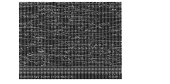
- FIG. 1 shows a scanning electron microscope observation image of a cross section of a conventional sintered layer (not including electrically insulating particles) using aluminum flakes.
- FIG. 2 shows a scanning electron microscope observation image of the cross section of the sintered layer of the electrode material of the present invention using aluminum flakes and electrically insulating particles.
- FIG. 1 the gap between the aluminum flakes is crushed, and the surface area of the aluminum flakes is not fully utilized.
- FIG. 2 it can be confirmed that electrically insulating particles have entered between the aluminum flakes and an appropriate space is maintained between the flakes.
- the effect of using electrostatic insulating particles as a spacer to increase the capacitance is not limited to the use of scaly powders, but also when using powders of various shapes. Has been confirmed.
- the shape of the sintered layer is not particularly limited, but is generally preferably a foil having an average thickness of 5 to 1000 ⁇ m, particularly 5 to 50 ⁇ m.
- the average thickness is an average of 10 measured values measured with a micrometer.
- the electrode material of the present invention may have a base material that supports the sintered layer.
- a base material for example, an aluminum foil can be suitably used.
- the aluminum foil as the substrate is not particularly limited, and pure aluminum or aluminum alloy can be used.
- the aluminum foil used in the present invention is composed of silicon (Si), iron (Fe), copper (Cu), manganese (Mn), magnesium (Mg), chromium (Cr), zinc (Zn), titanium (
- the content of the aluminum alloy or the above unavoidable impurity elements to which at least one alloy element of Ti), vanadium (V), gallium (Ga), nickel (Ni), boron (B) is added within the necessary range is limited. Also included aluminum.
- the thickness of the aluminum foil is not particularly limited, but is preferably in the range of 5 to 100 ⁇ m, particularly 10 to 50 ⁇ m.
- the above aluminum foil can be manufactured by a known method. For example, a molten aluminum or aluminum alloy having the above predetermined composition is prepared, and an ingot obtained by casting the molten metal is appropriately homogenized. Thereafter, an aluminum foil can be obtained by subjecting the ingot to hot rolling and cold rolling.
- an intermediate annealing treatment may be performed in the range of 50 to 500 ° C., particularly 150 to 400 ° C.
- a soft foil may be obtained by performing an annealing treatment within a range of 150 to 650 ° C., particularly 350 to 550 ° C.
- the sintered layer is formed on one side or both sides of the base material.
- the electrode material of the present invention when used for a low-voltage capacitor used at a low voltage of 100 V or less, it can exhibit a performance higher than that of an electrode material obtained by a conventional etching process. It can utilize suitably for the use of.
- the electrode material of the present invention when used as an electrode for an aluminum electrolytic capacitor, the electrode material can be used without etching treatment. That is, the electrode material of the present invention can be used as an electrode (electrode foil) as it is or without being subjected to etching treatment or by anodizing treatment.
- An anode foil using the electrode material of the present invention and a cathode foil are laminated with a separator interposed therebetween, and wound to form a capacitor element.
- the capacitor element is impregnated with an electrolytic solution, and the capacitor element includes the electrolytic solution. Is stored in an exterior case, and the case is sealed with a sealing body to obtain an electrolytic capacitor.
- the method for producing the electrode material for aluminum electrolytic capacitor of the present invention comprises: A first step of forming a film comprising a paste-like composition containing at least one powder of aluminum and an aluminum alloy and electrically insulating particles; and sintering the film at a temperature of 400 to 660 ° C. A second step of forming a layer; And an etching process is not included.
- the first step forms a film made of a paste-like composition containing at least one powder of aluminum and an aluminum alloy and electrically insulating particles.
- composition (component) of aluminum and aluminum alloy those listed above can be used.
- powder for example, pure aluminum powder having an aluminum purity of 99.8% by weight or more is preferably used.
- electrically insulating particles those listed above can be used.
- films when using a substrate, those listed above can be used.
- the paste composition may contain a resin binder, a solvent, a sintering aid, a surfactant, and the like as necessary in addition to the powder and the electrically insulating particles. Any of these may be known or commercially available. In particular, it is preferable to use at least one of a resin binder and a solvent as a paste-like composition, whereby a film can be efficiently formed.
- the resin binder is not limited.
- a synthetic resin such as epoxy resin, urea resin, phenol resin, acrylonitrile resin, cellulose resin, paraffin wax, polyethylene wax, or natural resin such as wax, tar, glue, urushi, pine resin, beeswax, or wax can be preferably used.
- resin binders are classified into those that volatilize when heated, depending on the molecular weight, the type of resin, etc., and those that remain together with the aluminum powder due to thermal decomposition, and can be used properly according to the desired electrostatic properties. it can.
- solvents can be used.
- organic solvents such as ethanol, toluene, ketones, and esters can be used.
- the paste composition can be formed by using a coating method such as roller, brush, spray, dipping, or the like, or can be formed by a known printing method such as silk screen printing.
- the film When using a substrate, the film is formed on one or both sides of the substrate. When forming on both surfaces, it is preferable to arrange
- the thickness of the film is not limited, but the film is preferably formed so that the average thickness of the sintered layer obtained after sintering is 5 to 1000 ⁇ m, particularly 5 to 50 ⁇ m.
- the film may be dried at a temperature within the range of 20 to 300 ° C., if necessary.
- the coating is sintered at a temperature of 400 to 660 ° C. to form a sintered layer.
- the sintering temperature is 400 to 660 ° C., preferably 450 to 600 ° C.
- the sintering time varies depending on the sintering temperature and the like, but can usually be appropriately determined within a range of about 5 to 24 hours.
- the sintering atmosphere is not particularly limited, and may be any one of a vacuum atmosphere, an inert gas atmosphere, an oxidizing gas atmosphere (air), a reducing atmosphere, etc., and particularly a vacuum atmosphere or a reducing atmosphere. Is preferred.
- the pressure condition may be normal pressure, reduced pressure or increased pressure.
- the first step it is preferable to perform a heat treatment (degreasing treatment) in a temperature range of 100 to 600 ° C. for a holding time of 5 hours or more in advance before the second step.
- the heat treatment atmosphere is not particularly limited, and may be any of a vacuum atmosphere, an inert gas atmosphere, or an oxidizing gas atmosphere, for example.
- the pressure condition may be normal pressure, reduced pressure, or increased pressure.
- the electrode material of the present invention is obtained. This can be used as it is as an electrode for an aluminum electrolytic capacitor (electrode foil) without etching.
- the electrode material can be formed as an electrode by subjecting it to an anodization treatment as a third step as necessary, thereby forming a dielectric.
- the anodizing treatment conditions are not particularly limited, but are usually from 10 mA / cm 2 to 400 mA / cm 2 in a boric acid solution or an ammonium adipate aqueous solution having a concentration of 0.01 mol to 5 mol and a temperature of 30 ° C. to 100 ° C. It is sufficient to apply a current of about 5 minutes or more.
- the electrode material for an aluminum electrolytic capacitor of the present invention forms a sintered layer by sintering at least one powder of aluminum and an aluminum alloy through electrically insulating particles.
- the effective surface area is ensured by suppressing excessive necking (over-sintering) as much as possible and reducing the contact area between the powders as much as possible. Therefore, even when the electrode material for an aluminum electrolytic capacitor of the present invention is used for a low-voltage capacitor used at a low voltage of 100 V or less, it can exhibit performances higher than that of an electrode material obtained by a conventional etching process.
- Examples 1-1 to 1-5 and Comparative Example 1-1 Uniformly disperse aluminum powder with an average particle size of 3 ⁇ m (high-purity aluminum powder of 99.99% or more, aspect ratio (average particle size / average thickness) 1) and alumina particles with an average particle size of 0.5 ⁇ m in the following ratio:
- a sintered body was produced in which the coated film was laminated on both sides of a 20 ⁇ m aluminum foil base material (high purity aluminum foil of 99.99% or more) by 50 ⁇ m.
- the average particle size was measured using a microtrack manufactured by Nikkiso Co., Ltd.
- an anodic oxidation treatment was performed using an ammonium adipate aqueous solution.
- the conditions of the anodizing treatment were such that the concentration of the aqueous solution was 0.3 mol, the temperature was 60 ° C., and a current of 25 mA / cm 2 was applied for 10 minutes.
- Example 1-1 Ratio of aluminum powder to alumina particles (aluminum powder: alumina particles)
- Aluminum powder 100% The capacitance of each electrode material is shown in Table 1 below.
- the capacity is higher in all voltage regions than BL.
- Examples 2-1 to 2-5 and Comparative Example 2-1 Aluminum powder having an average particle diameter of 80 ⁇ m (high-purity aluminum powder of 99.99% or more, aspect ratio (average particle diameter / average thickness) 1) and alumina particles having an average particle diameter of 5 ⁇ m were uniformly dispersed at the following ratio: A sintered body was produced in which the coating film was laminated on both sides by 100 ⁇ m on a 20 ⁇ m aluminum foil base material (high purity aluminum foil of 99.99% or more).
- an anodic oxidation treatment was performed using an ammonium adipate aqueous solution.
- the conditions of the anodizing treatment were such that the concentration of the aqueous solution was 0.3 mol, the temperature was 60 ° C., and a current of 25 mA / cm 2 was applied for 10 minutes.
- Example 2-1 200: 1 (weight ratio), 300: 1 (volume ratio)
- Aluminum powder 100% The capacitance of each electrode material is shown in Table 2 below.
- Examples 3-1 to 3-7 and Comparative Example 3-1 Coating in which aluminum flakes having an average particle diameter of 5 ⁇ m and aspect ratio (average particle diameter / average thickness) 5 (5 ⁇ m / 1 ⁇ m) and alumina particles having an average particle diameter of 0.5 ⁇ m are uniformly dispersed in the following ratio:
- a sintered body was prepared in which the film was laminated on both sides by 50 ⁇ m on a 20 ⁇ m aluminum foil base material (high purity aluminum foil of 99.99% or more).
- an anodic oxidation treatment was performed using an ammonium adipate aqueous solution.
- the conditions of the anodizing treatment were such that the concentration of the aqueous solution was 0.3 mol, the temperature was 60 ° C., and a current of 25 mA / cm 2 was applied for 10 minutes.
- Example 3-1 Ratio of aluminum flakes to alumina particles (aluminum flakes: alumina particles)
- Example 3-7 1: 2 (weight ratio), 3: 4 (volume ratio) Comparative Example 3-1 (BL) 100% aluminum flakes
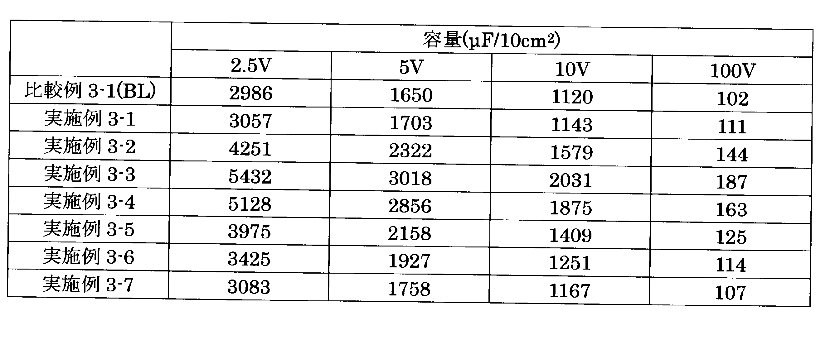
- the capacitance of each electrode material is shown in Table 3 below.
- the capacity was increased by about 80% from BL. It can be seen that when the scaly powder (aluminum flakes) is used, the effect of using the electrically insulating particles (alumina particles) in combination is larger than when the spherical powder is used.
- a sintered body was produced in which the coated film was laminated on both sides by 50 ⁇ m on a 20 ⁇ m aluminum foil base material (high purity aluminum foil of 99.99% or more).
- an anodic oxidation treatment was performed using an ammonium adipate aqueous solution.
- the conditions of the anodizing treatment were such that the concentration of the aqueous solution was 0.3 mol, the temperature was 60 ° C., and a current of 25 mA / cm 2 was applied for 10 minutes.
- Example 4-1 200: 1 (weight ratio), 300: 1 (volume ratio)
- the capacitance of each electrode material is shown in Table 4 below.
- Aluminum flakes with a very large aspect ratio have a low capacity in the BL state. This is because the cross-sectional state of the sintered layer is as shown in FIG. However, by dispersing alumina particles as spacers, the low pressure capacity (5 V) is up to 800 times.
- This capacity is far higher than the maximum capacity (5 V, 3600 ⁇ F / 10 cm 2 ) of an electrode material using an aluminum foil (hereinafter referred to as “etched foil”) obtained by a conventional etching process.
- the reason why the value of the 100V capacity is low is considered to be because it is difficult to form an oxide film having a sufficient withstand voltage of 100V with aluminum flakes having a thickness of less than 0.2 ⁇ m.
- a sintered body was prepared by laminating a laminate of 50 ⁇ m each on a 20 ⁇ m aluminum foil base material (high purity aluminum foil of 99.99% or more).
- an anodic oxidation treatment was performed using an ammonium adipate aqueous solution.
- the conditions of the anodizing treatment were such that the concentration of the aqueous solution was 0.3 mol, the temperature was 60 ° C., and a current of 25 mA / cm 2 was applied for 10 minutes.
- Example 5-1 200: 1 (weight ratio), 300: 1 (volume ratio)
- Example 5-7 1: 2 (weight ratio), 3: 4 (volume ratio) Comparative Example 5-1 (BL) 100% aluminum flakes
- a sintered body was prepared by laminating a laminate of 50 ⁇ m each on a 20 ⁇ m aluminum foil base material (high purity aluminum foil of 99.99% or more).
- an anodic oxidation treatment was performed using an ammonium adipate aqueous solution.
- the conditions of the anodizing treatment were such that the concentration of the aqueous solution was 0.3 mol, the temperature was 60 ° C., and a current of 25 mA / cm 2 was applied for 10 minutes.
- Example 6-1 200: 1 (weight ratio), 300: 1 (volume ratio)
- a sintered body was prepared by laminating a laminate of 50 ⁇ m each on a 20 ⁇ m aluminum foil base material (high purity aluminum foil of 99.99% or more).
- an anodic oxidation treatment was performed using an ammonium adipate aqueous solution.
- the conditions of the anodizing treatment were such that the concentration of the aqueous solution was 0.3 mol, the temperature was 60 ° C., and a current of 25 mA / cm 2 was applied for 10 minutes.
- Example 7-1 200: 1 (weight ratio), 300: 1 (volume ratio)
- the capacity value is almost the same as Examples 3-1 to 3-7. It can be seen that even if it is not alumina particles, it can function as a spacer as long as it has the same particle size and electrical insulation.
- Examples 8-1 to 8-9 and comparative examples 8-1 to 8-2 A coating film in which the following aluminum powders (1) to (9) and alumina particles having an average particle diameter of 0.01 ⁇ m are dispersed at a ratio of 10: 1 (weight ratio) is applied to a 20 ⁇ m aluminum foil substrate (99.99% or more A high-purity aluminum foil) was prepared by laminating 50 ⁇ m on both sides.
- Example 8-1 Average particle size 3 ⁇ m Aluminum powder with aspect ratio 1 (2)
- Example 8-2 Average particle size 3 ⁇ m Aluminum flakes with aspect ratio 3 (3 ⁇ m / 1 ⁇ m) (3)
- Example 8- 3 Average particle size 3 ⁇ m Aluminum flakes with aspect ratio 25 (3 ⁇ m / 0.12 ⁇ m) (4)
- Example 8-4 Average particle size 3 ⁇ m Aluminum flakes with aspect ratio 60 (3 ⁇ m / 0.05 ⁇ m) (5)
- Example 8- 5 Average particle size 5 ⁇ m Aluminum flakes with aspect ratio 5 (5 ⁇ m / 1 ⁇ m) (6)
- Example 8-6 Average particle size 5 ⁇ m Aluminum flakes with aspect ratio 100 (5 ⁇ m / 0.05 ⁇ m) (7)
- Example 8-7 Average particle size 10 ⁇ m Aluminum flakes with aspect ratio 25 (10 ⁇ m / 0.4 ⁇ m) (8)
- Example 8-8 Average particle size 10 ⁇ m Aluminum flakes with aspect ratio 200 (10 ⁇ m / 0.05 ⁇ m) (9)
- Example 8-9 Average particle size 10 ⁇ m Aluminum
- High capacity can be obtained by dispersing alumina particles having an average particle size of 0.01 ⁇ m with respect to aluminum powder having various particle sizes and aspect ratios. It can also be seen that the larger the aspect ratio, the greater the effect.
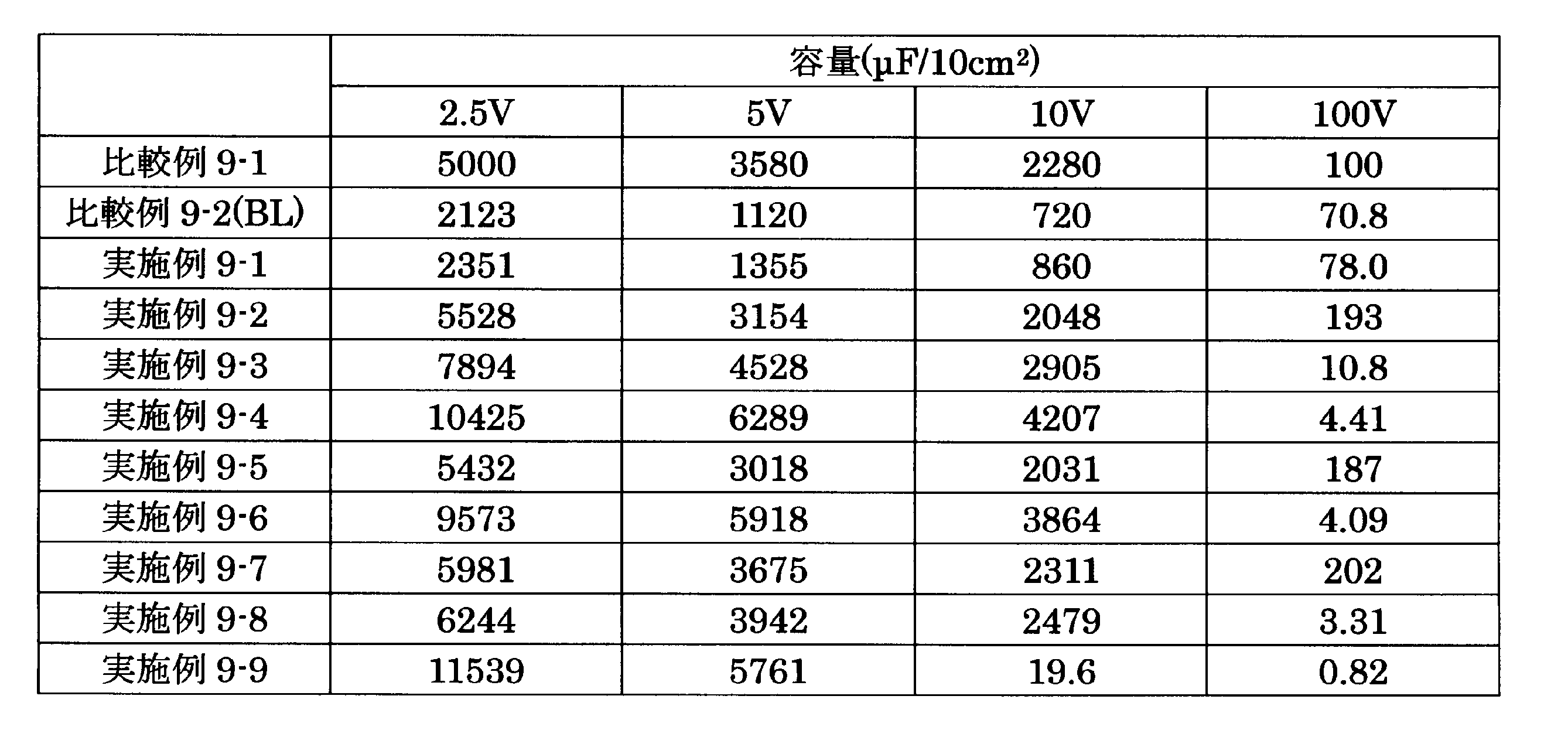
- Example 8-2 In Comparative Example 8-2 (BL), it does not reach the maximum capacity of the etched foil, but in Example 8-7, it exceeds the maximum capacity of the etched foil in all voltage regions of 100 V or less.
- Examples 8-3, 8-4, 8-6, and 8-8 have excellent capacity at 10 V or less.
- the thickness of the aluminum flakes is less than 0.02 ⁇ m as in Example 8-9, the withstand voltage film having a sufficient thickness is not formed, so that the capacity becomes low even at 10V.
- Examples 8-2 and 8-5 also have values exceeding the etched foil in the 100V region.
- the capacity of Example 8-1 also tends to be higher than that of BL.
- the capacity value of 150 V is 51.2 ⁇ F, which is confirmed to exceed the capacity of the etched foil (about 48 ⁇ F).
- an electrode having a higher capacity than the etched foil can be obtained in any voltage region.
- Aluminum flakes having an aspect ratio of 1000 are liable to cause coating drying failure and degreasing failure during heat treatment in the production process of the laminated foil, and it is difficult to obtain a stable product.
- Examples 9-1 to 9-9 and Comparative Examples 9-1 to 9-2 A coating film in which the following aluminum powders (1) to (9) and alumina particles having an average particle diameter of 0.5 ⁇ m are dispersed at a ratio of 10: 1 (weight ratio) is applied to a 20 ⁇ m aluminum foil substrate (99.99% or more A high-purity aluminum foil) was prepared by laminating 50 ⁇ m on both sides.
- Example 9-1 Average particle size 3 ⁇ m Aluminum powder with aspect ratio 1 (2)
- Example 9-2 Average particle size 3 ⁇ m Aluminum flakes with aspect ratio 3 (3 ⁇ m / 1 ⁇ m) (3)
- Example 9- 3 Average particle size 3 ⁇ m Aluminum flakes with aspect ratio 25 (3 ⁇ m / 0.12 ⁇ m) (4)
- Example 9-4 Average particle size 3 ⁇ m Aluminum flakes with aspect ratio 60 (3 ⁇ m / 0.05 ⁇ m) (5)
- Example 9- 5 Average particle size 5 ⁇ m Aluminum flakes with aspect ratio 5 (5 ⁇ m / 1 ⁇ m) (6)
- Example 9-6 Average particle size 5 ⁇ m Aluminum flakes with aspect ratio 100 (5 ⁇ m / 0.05 ⁇ m) (7)
- Example 9-7 Average particle size 10 ⁇ m Aluminum flakes with aspect ratio 25 (10 ⁇ m / 0.4 ⁇ m) (8)
- Example 9-8 Average particle size 10 ⁇ m Aluminum flakes with aspect ratio 200 (10 ⁇ m / 0.05 ⁇ m) (9)
- Example 9-9 Average particle size 10 ⁇ m Aluminum
Landscapes
- Engineering & Computer Science (AREA)
- Chemical & Material Sciences (AREA)
- Power Engineering (AREA)
- Materials Engineering (AREA)
- Organic Chemistry (AREA)
- Metallurgy (AREA)
- Electrochemistry (AREA)
- Chemical Kinetics & Catalysis (AREA)
- Microelectronics & Electronic Packaging (AREA)
- Mechanical Engineering (AREA)
- Composite Materials (AREA)
- Manufacturing & Machinery (AREA)
- Powder Metallurgy (AREA)
Abstract
Description
1.アルミニウム及びアルミニウム合金の少なくとも1種の粉末が電気絶縁性粒子を介して焼結した焼結層を有することを特徴とするアルミニウム電解コンデンサ用電極材。
2.前記粉末と前記電気絶縁性粒子との含有量の重量比が1:2~200:1である、上記項1に記載のアルミニウム電解コンデンサ用電極材。
3.前記粉末のアスペクト比が1~1000である、上記項1又は2に記載のアルミニウム電解コンデンサ用電極材。
4.前記粉末の平均粒径が1~80μmである、上記項1~3のいずれかに記載のアルミニウム電解コンデンサ用電極材。
5.前記粉末の平均厚みが0.01~80μmである、上記項1~4のいずれかに記載のアルミニウム電解コンデンサ用電極材。
6.前記電気絶縁性粒子が金属酸化物又は金属窒化物である、上記項1~5のいずれかに記載のアルミニウム電解コンデンサ用電極材。
7.前記電気絶縁性粒子がアルミナ、チタニア、ジルコニア及びシリカからなる群から選択される少なくとも1種である、上記項1~6のいずれかに記載のアルミニウム電解コンデンサ用電極材。
8.前記電気絶縁性粒子の平均粒径が0.01~10μmである、上記項1~7のいずれかに記載のアルミニウム電解コンデンサ用電極材。
9.前記焼結層の平均厚みが5~1000μmである、上記項1~8のいずれかに記載のアルミニウム電解コンデンサ用電極材。
10.前記焼結層を支持する基材を有する、上記項1~9のいずれかに記載のアルミニウム電解コンデンサ用電極材。
11.アルミニウム及びアルミニウム合金の少なくとも1種の粉末並びに電気絶縁性粒子を含有するペースト状組成物からなる皮膜を形成する第1工程、及び
前記皮膜を400~660℃の温度で焼結することにより焼結層を形成する第2工程、
を含み、且つ、エッチング工程を含まないことを特徴とするアルミニウム電解コンデンサ用電極材の製造方法。
12.前記焼結層を陽極酸化処理する第3工程を更に有する、上記項11に記載の製造方法。
本発明のアルミニウム電解コンデンサ用電極材は、アルミニウム及びアルミニウム合金の少なくとも1種の粉末が電気絶縁性粒子(スペーサーとして作用する)を介して焼結した焼結層を有することを特徴とする。以下、アルミニウム及びアルミニウム合金の少なくとも1種の粉末を単に「粉末」とも言う。
本発明のアルミニウム電解コンデンサ用電極材の製造方法は、
アルミニウム及びアルミニウム合金の少なくとも1種の粉末並びに電気絶縁性粒子を含有するペースト状組成物からなる皮膜を形成する第1工程、及び
前記皮膜を400~660℃の温度で焼結することにより焼結層を形成する第2工程、
を含み、且つ、エッチング工程を含まないことを特徴とする。
(第1工程)
第1工程は、アルミニウム及びアルミニウム合金の少なくとも1種の粉末並びに電気絶縁性粒子を含有するペースト状組成物からなる皮膜を形成する。
(第2工程)
第2工程は、皮膜を400~660℃の温度で焼結することにより焼結層を形成する。
(第3工程)
前記の第2工程において、本発明の電極材が得られる。これは、エッチング処理を施すことなく、そのままアルミニウム電解コンデンサ用電極(電極箔)として用いることが可能である。一方、前記電極材は、必要に応じて第3工程として陽極酸化処理を施すことにより誘電体を形成させることができ、これを電極とすることができる。
平均粒径が3μmのアルミニウム粉末(99.99%以上の高純度アルミニウム粉末、アスペクト比(平均粒径/平均厚み)1)と平均粒径が0.5μmのアルミナ粒子とを下記の比で均一に分散させた塗膜を、20μmのアルミニウム箔基材(99.99%以上の高純度アルミニウム箔)に50μmずつ両面積層した焼結体を作製した。平均粒径の測定は、日機装株式会社製マイクロトラックを用いて行った。
実施例1-1 200:1(重量比)、300:1(体積比)
実施例1-2 20:1(重量比)、 30:1(体積比)
実施例1-3 10:1(重量比)、 15:1(体積比)
実施例1-4 5:1(重量比)、 15:2(体積比)
実施例1-5 2:1(重量比)、 3:1(体積比)
比較例1-1(ブランクテスト:以下「BL」) アルミニウム粉末100%
各電極材の静電容量を下記表1に示す。

平均粒径が80μmのアルミニウム粉末(99.99%以上の高純度アルミニウム粉末、アスペクト比(平均粒径/平均厚み)1)と平均粒径が5μmのアルミナ粒子とを下記の比で均一に分散させた塗膜を、20μmのアルミニウム箔基材(99.99%以上の高純度アルミニウム箔)に100μmずつ両面積層した焼結体を作製した。
実施例2-1 200:1(重量比)、300:1(体積比)
実施例2-2 20:1(重量比)、30:1(体積比)
実施例2-3 10:1(重量比)、15:1(体積比)
実施例2-4 5:1(重量比)、15:2(体積比)
実施例2-5 2:1(重量比)、3:1(体積比)
比較例2-1(BL) アルミニウム粉末100%
各電極材の静電容量を下記表2に示す。

平均粒径が5μm、アスペクト比(平均粒径/平均厚み)=5(5μm/1μm)のアルミフレークと、平均粒径が0.5μmのアルミナ粒子とを下記の比で均一に分散させた塗膜を、20μmのアルミニウム箔基材(99.99%以上の高純度アルミニウム箔)に50μmずつ両面積層した焼結体を作製した。
実施例3-1 200:1(重量比)、300:1(体積比)
実施例3-2 20:1(重量比)、 30:1(体積比)
実施例3-3 10:1(重量比)、 15:1(体積比)
実施例3-4 5:1(重量比)、 15:2(体積比)
実施例3-5 2:1(重量比)、 3:1(体積比)
実施例3-6 1:1(重量比)、 3:2(体積比)
実施例3-7 1:2(重量比)、 3:4(体積比)
比較例3-1(BL) アルミフレーク100%
各電極材の静電容量を下記表3に示す。
平均粒径が5μm、アスペクト比(平均粒径/平均厚み)=100(5μm/0.05μm)のアルミフレークと、平均粒径が0.01μmのアルミナ粒子とを下記の比で均一に分散させた塗膜を、20μmのアルミニウム箔基材(99.99%以上の高純度アルミニウム箔)に50μmずつ両面積層した焼結体を作製した。
実施例4-1 200:1(重量比)、300:1(体積比)
実施例4-2 20:1(重量比)、30:1(体積比)
実施例4-3 10:1(重量比)、15:1(体積比)
実施例4-4 5:1(重量比)、15:2(体積比)
実施例4-5 2:1(重量比)、3:1(体積比)
実施例4-6 1:1(重量比)、3:2(体積比)
実施例4-7 1:2(重量比)、3:4(体積比)
比較例4-1(BL) アルミフレーク100%
各電極材の静電容量を下記表4に示す。

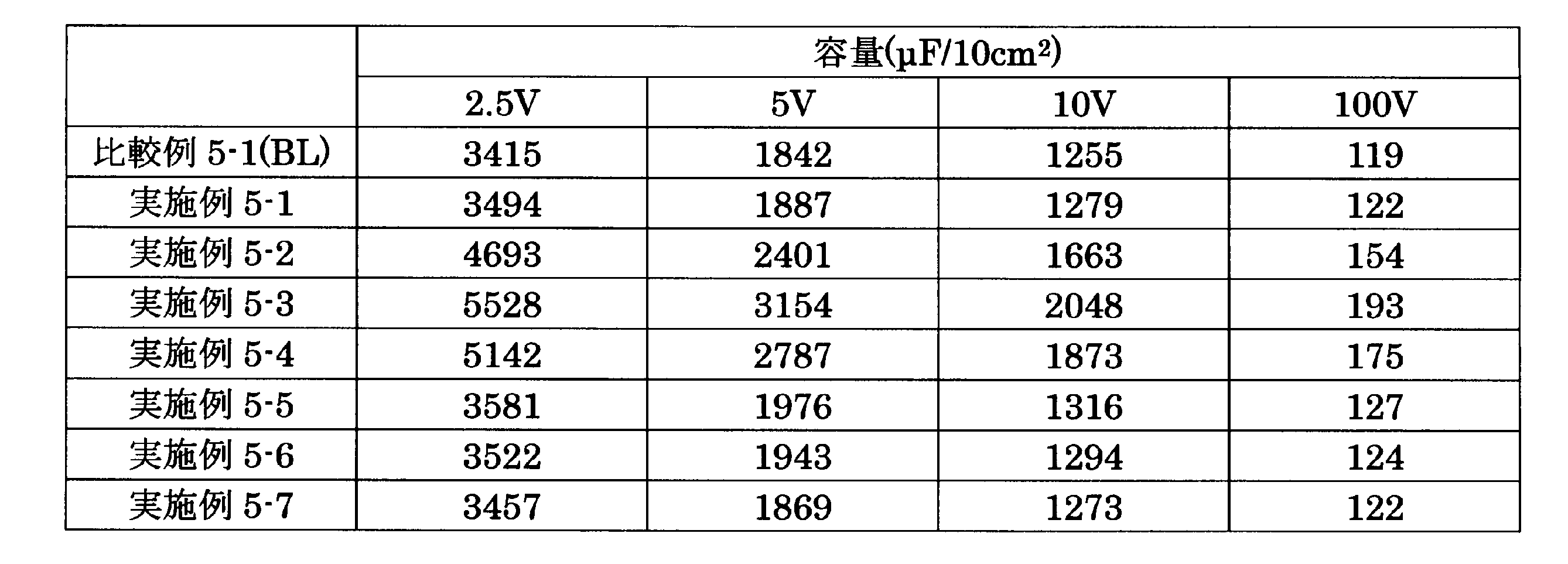
平均粒径が3μm、アスペクト比(平均粒径/平均厚み)=3(3μm/1μm)のアルミフレークと平均粒径が0.5μmのアルミナ粒子とを下記重量比で均一に分散させた塗膜を、20μmのアルミニウム箔基材(99.99%以上の高純度アルミニウム箔)に50μmずつ両面積層した焼結体を作製した。
実施例5-1 200:1(重量比)、300:1(体積比)
実施例5-2 20:1(重量比)、30:1(体積比)
実施例5-3 10:1(重量比)、15:1(体積比)
実施例5-4 5:1(重量比)、15:2(体積比)
実施例5-5 2:1(重量比)、3:1(体積比)
実施例5-6 1:1(重量比)、3:2(体積比)
実施例5-7 1:2(重量比)、3:4(体積比)
比較例5-1(BL) アルミフレーク100%
平均粒径が10μm、アスペクト比(平均粒径/平均厚み)=10(10μm/1μm)のアルミフレークと平均粒径が0.5μmのアルミナ粒子とを下記重量比で均一に分散させた塗膜を、20μmのアルミニウム箔基材(99.99%以上の高純度アルミニウム箔)に50μmずつ両面積層した焼結体を作製した。
実施例6-1 200:1(重量比)、300:1(体積比)
実施例6-2 20:1(重量比)、30:1(体積比)
実施例6-3 10:1(重量比)、15:1(体積比)
実施例6-4 5:1(重量比)、15:2(体積比)
実施例6-5 2:1(重量比)、3:1(体積比)
実施例6-6 1:1(重量比)、3:2(体積比)
実施例6-7 1:2(重量比)、3:4(体積比)
比較例6-1(BL) アルミフレーク100%

平均粒径が5μm、アスペクト比(平均粒径/平均厚み)=5(5μm/1μm)のアルミフレークと、平均粒径0.5μmのチタニア粒子とを下記重量比で均一に分散させた塗膜を、20μmのアルミニウム箔基材(99.99%以上の高純度アルミニウム箔)に50μmずつ両面積層した焼結体を作製した。
実施例7-1 200:1(重量比)、300:1(体積比)
実施例7-2 20:1(重量比)、30:1(体積比)
実施例7-3 10:1(重量比)、15:1(体積比)
実施例7-4 5:1(重量比)、15:2(体積比)
実施例7-5 2:1(重量比)、3:1(体積比)
実施例7-6 1:1(重量比)、3:2(体積比)
実施例7-7 1:2(重量比)、3:4(体積比)
比較例7-1(BL) アルミフレーク100%

下記アルミニウム粉末(1)~(9)と平均粒径が0.01μmのアルミナ粒子とを10:1(重量比)の比率で分散させた塗膜を、20μmのアルミニウム箔基材(99.99%以上の高純度アルミニウム箔)に50μmずつ両面積層した焼結体を作製した。
(1)実施例8-1 平均粒径=3μm アスペクト比1のアルミニウム粉末
(2)実施例8-2 平均粒径=3μm アスペクト比3(3μm/1μm)のアルミフレーク
(3)実施例8-3 平均粒径=3μm アスペクト比25(3μm/0.12μm)のアルミフレーク
(4)実施例8-4 平均粒径=3μm アスペクト比60(3μm/0.05μm)のアルミフレーク
(5)実施例8-5 平均粒径=5μm アスペクト比5(5μm/1μm)のアルミフレーク
(6)実施例8-6 平均粒径=5μm アスペクト比100(5μm/0.05μm)のアルミフレーク
(7)実施例8-7 平均粒径=10μm アスペクト比25(10μm/0.4μm)のアルミフレーク
(8)実施例8-8 平均粒径=10μm アスペクト比200(10μm/0.05μm)のアルミフレーク
(9)実施例8-9 平均粒径=10μm アスペクト比1000 (10μm/0.01μm)のアルミフレーク
比較例8-1 エッチド箔最高レベルの容量
比較例8-2(BL) 平均粒径が3μm アスペクト比1のアルミニウム粉末(アルミニウム粉末のみの従来積層箔)

下記アルミニウム粉末(1)~(9)と平均粒径が0.5μmのアルミナ粒子とを10:1(重量比)の比率で分散させた塗膜を、20μmのアルミニウム箔基材(99.99%以上の高純度アルミニウム箔)に50μmずつ両面積層した焼結体を作製した。
(1)実施例9-1 平均粒径=3μm アスペクト比1のアルミニウム粉末
(2)実施例9-2 平均粒径=3μm アスペクト比3(3μm/1μm)のアルミフレーク
(3)実施例9-3 平均粒径=3μm アスペクト比25(3μm/0.12μm)のアルミフレーク
(4)実施例9-4 平均粒径=3μm アスペクト比60(3μm/0.05μm)のアルミフレーク
(5)実施例9-5 平均粒径=5μm アスペクト比5(5μm/1μm)のアルミフレーク
(6)実施例9-6 平均粒径=5μm アスペクト比100(5μm/0.05μm)のアルミフレーク
(7)実施例9-7 平均粒径=10μm アスペクト比25(10μm/0.4μm)のアルミフレーク
(8)実施例9-8 平均粒径=10μm アスペクト比200(10μm/0.05μm)のアルミフレーク
(9)実施例9-9 平均粒径=10μm アスペクト比1000 (10μm/0.01μm)のアルミフレーク
比較例9-1 エッチド箔最高レベルの容量
比較例9-2(BL) 平均粒径が3μm、アスペクト比1のアルミニウム粉末(アルミニウム粉末のみの従来積層箔)
Claims (12)
- アルミニウム及びアルミニウム合金の少なくとも1種の粉末が電気絶縁性粒子を介して焼結した焼結層を有することを特徴とするアルミニウム電解コンデンサ用電極材。
- 前記粉末と前記電気絶縁性粒子との含有量の重量比が1:2~200:1である、請求項1に記載のアルミニウム電解コンデンサ用電極材。
- 前記粉末のアスペクト比が1~1000である、請求項1又は2に記載のアルミニウム電解コンデンサ用電極材。
- 前記粉末の平均粒径が1~80μmである、請求項1~3のいずれかに記載のアルミニウム電解コンデンサ用電極材。
- 前記粉末の平均厚みが0.01~80μmである、請求項1~4のいずれかに記載のアルミニウム電解コンデンサ用電極材。
- 前記電気絶縁性粒子が金属酸化物又は金属窒化物である、請求項1~5のいずれかに記載のアルミニウム電解コンデンサ用電極材。
- 前記電気絶縁性粒子がアルミナ、チタニア、ジルコニア及びシリカからなる群から選択される少なくとも1種である、請求項1~6のいずれかに記載のアルミニウム電解コンデンサ用電極材。
- 前記電気絶縁性粒子の平均粒径が0.01~10μmである、請求項1~7のいずれかに記載のアルミニウム電解コンデンサ用電極材。
- 前記焼結層の平均厚みが5~1000μmである、請求項1~8のいずれかに記載のアルミニウム電解コンデンサ用電極材。
- 前記焼結層を支持する基材を有する、請求項1~9のいずれかに記載のアルミニウム電解コンデンサ用電極材。
- アルミニウム及びアルミニウム合金の少なくとも1種の粉末並びに電気絶縁性粒子を含有するペースト状組成物からなる皮膜を形成する第1工程、及び
前記皮膜を400~660℃の温度で焼結することにより焼結層を形成する第2工程、
を含み、且つ、エッチング工程を含まないことを特徴とするアルミニウム電解コンデンサ用電極材の製造方法。 - 前記焼結層を陽極酸化処理する第3工程を更に有する、請求項11に記載の製造方法。
Priority Applications (2)
| Application Number | Priority Date | Filing Date | Title |
|---|---|---|---|
| JP2015530873A JP6461794B2 (ja) | 2013-08-05 | 2014-08-04 | アルミニウム電解コンデンサ用電極材及びその製造方法 |
| CN201480040537.9A CN105393320B (zh) | 2013-08-05 | 2014-08-04 | 铝电解电容器用电极材料及其制造方法 |
Applications Claiming Priority (2)
| Application Number | Priority Date | Filing Date | Title |
|---|---|---|---|
| JP2013-162271 | 2013-08-05 | ||
| JP2013162271 | 2013-08-05 |
Publications (1)
| Publication Number | Publication Date |
|---|---|
| WO2015019987A1 true WO2015019987A1 (ja) | 2015-02-12 |
Family
ID=52461319
Family Applications (1)
| Application Number | Title | Priority Date | Filing Date |
|---|---|---|---|
| PCT/JP2014/070446 Ceased WO2015019987A1 (ja) | 2013-08-05 | 2014-08-04 | アルミニウム電解コンデンサ用電極材及びその製造方法 |
Country Status (4)
| Country | Link |
|---|---|
| JP (1) | JP6461794B2 (ja) |
| CN (1) | CN105393320B (ja) |
| TW (1) | TWI656549B (ja) |
| WO (1) | WO2015019987A1 (ja) |
Cited By (5)
| Publication number | Priority date | Publication date | Assignee | Title |
|---|---|---|---|---|
| WO2016158492A1 (ja) * | 2015-03-31 | 2016-10-06 | 東洋アルミニウム株式会社 | アルミニウム電解コンデンサ用電極材及びその製造方法 |
| JPWO2021079813A1 (ja) * | 2019-10-21 | 2021-04-29 | ||
| CN115274304A (zh) * | 2022-08-02 | 2022-11-01 | 新疆众和股份有限公司 | 烧结箔及其制备方法 |
| CN116174724A (zh) * | 2021-11-26 | 2023-05-30 | 新疆众和股份有限公司 | 一种高比容电解电容器阳极箔的制备方法 |
| JP2024530574A (ja) * | 2022-08-02 | 2024-08-23 | 南通海星電子股▲フン▼有限公司 | 高誘電性複合粉末焼結箔の製造方法 |
Families Citing this family (9)
| Publication number | Priority date | Publication date | Assignee | Title |
|---|---|---|---|---|
| CN116230412A (zh) * | 2016-03-31 | 2023-06-06 | 日本贵弥功株式会社 | 电极箔、其制造方法、卷绕型的电容器及其制造方法 |
| CN109036852B (zh) * | 2018-08-13 | 2020-09-18 | 浙江华义瑞东新材料有限公司 | 一种三维多孔铝电极箔及其制备方法 |
| CN111627714B (zh) * | 2020-05-28 | 2021-08-13 | 西安交通大学 | 一种具有多级混合结构的多孔阳极铝箔的制备方法 |
| CN113658803B (zh) * | 2021-08-24 | 2022-08-30 | 西安稀有金属材料研究院有限公司 | 一种铝电解电容器阳极烧结箔用双组分铝浆及其制备方法 |
| CN113458143B (zh) * | 2021-09-02 | 2021-11-23 | 西安稀有金属材料研究院有限公司 | 一种利用冷轧机制备铝电解电容器阳极箔的方法 |
| CN114512345B (zh) * | 2021-12-30 | 2025-11-11 | 浙江洪量新材科技有限公司 | 一种高比容多孔电极箔及其制备方法 |
| CN115083784B (zh) * | 2022-07-15 | 2024-01-02 | 新疆众和股份有限公司 | 烧结箔用浆料、烧结箔及其制备方法和铝电解电容器 |
| CN115188598B (zh) * | 2022-08-30 | 2024-05-28 | 西安稀有金属材料研究院有限公司 | 一种纳米介电粉包覆的铝电解电容器烧结箔及其制备方法 |
| CN119361325B (zh) * | 2024-12-25 | 2025-04-18 | 河南微纳电子材料有限公司 | 一种烧结箔用浆料及其制备方法 |
Citations (4)
| Publication number | Priority date | Publication date | Assignee | Title |
|---|---|---|---|---|
| JPS55165621A (en) * | 1979-06-08 | 1980-12-24 | Nippon Electric Co | Method of manufacturing sintered condenser element |
| JPS60229327A (ja) * | 1984-04-27 | 1985-11-14 | 日本電気株式会社 | 電解コンデンサ用多孔質陽極体の製造方法 |
| JP2013073984A (ja) * | 2011-09-27 | 2013-04-22 | Hitachi Aic Inc | 電解コンデンサの電極用の焼結体シートおよびその製造方法 |
| JP2013157392A (ja) * | 2012-01-27 | 2013-08-15 | Tdk Corp | 多孔質アルミニウム焼結体、固体電解コンデンサ用陽極電極材及び固体電解コンデンサ |
Family Cites Families (5)
| Publication number | Priority date | Publication date | Assignee | Title |
|---|---|---|---|---|
| DE2610224C2 (de) * | 1976-03-11 | 1983-01-05 | Fa. Hermann C. Starck Berlin, 1000 Berlin | Verfahren zur Herstellung von porösen Anodenkörpern durch Pressen und Sintern von Pulvern aus Ventilmetallen |
| DE3232245A1 (de) * | 1982-08-30 | 1984-03-01 | Hermann C. Starck Berlin, 1000 Berlin | Verbesserung der fliessfaehigkeit und erhoehung der schuettdichte von hochkapazitiven ventilmetallpulvern |
| EP1618575B1 (en) * | 2003-04-28 | 2019-10-23 | Showa Denko K.K. | Valve acting metal sintered body, production method therefor and solid electrolytic capacitor |
| JP4958510B2 (ja) * | 2006-10-10 | 2012-06-20 | 東洋アルミニウム株式会社 | アルミニウム電解コンデンサ用電極材及びその製造方法 |
| CN101191224A (zh) * | 2006-11-24 | 2008-06-04 | 横店集团东磁有限公司 | 一种铝电解电容器用阳极箔的制造方法 |
-
2014
- 2014-08-04 JP JP2015530873A patent/JP6461794B2/ja active Active
- 2014-08-04 TW TW103126581A patent/TWI656549B/zh active
- 2014-08-04 CN CN201480040537.9A patent/CN105393320B/zh active Active
- 2014-08-04 WO PCT/JP2014/070446 patent/WO2015019987A1/ja not_active Ceased
Patent Citations (4)
| Publication number | Priority date | Publication date | Assignee | Title |
|---|---|---|---|---|
| JPS55165621A (en) * | 1979-06-08 | 1980-12-24 | Nippon Electric Co | Method of manufacturing sintered condenser element |
| JPS60229327A (ja) * | 1984-04-27 | 1985-11-14 | 日本電気株式会社 | 電解コンデンサ用多孔質陽極体の製造方法 |
| JP2013073984A (ja) * | 2011-09-27 | 2013-04-22 | Hitachi Aic Inc | 電解コンデンサの電極用の焼結体シートおよびその製造方法 |
| JP2013157392A (ja) * | 2012-01-27 | 2013-08-15 | Tdk Corp | 多孔質アルミニウム焼結体、固体電解コンデンサ用陽極電極材及び固体電解コンデンサ |
Cited By (10)
| Publication number | Priority date | Publication date | Assignee | Title |
|---|---|---|---|---|
| WO2016158492A1 (ja) * | 2015-03-31 | 2016-10-06 | 東洋アルミニウム株式会社 | アルミニウム電解コンデンサ用電極材及びその製造方法 |
| JPWO2016158492A1 (ja) * | 2015-03-31 | 2018-01-25 | 東洋アルミニウム株式会社 | アルミニウム電解コンデンサ用電極材及びその製造方法 |
| JPWO2021079813A1 (ja) * | 2019-10-21 | 2021-04-29 | ||
| WO2021079813A1 (ja) * | 2019-10-21 | 2021-04-29 | 日本軽金属株式会社 | アルミニウム部材、イムノクロマトグラフィー用テストストリップ及びアルミニウム部材の製造方法 |
| JP7235889B2 (ja) | 2019-10-21 | 2023-03-08 | 日本軽金属株式会社 | アルミニウム部材、イムノクロマトグラフィー用テストストリップ及びアルミニウム部材の製造方法 |
| CN116174724A (zh) * | 2021-11-26 | 2023-05-30 | 新疆众和股份有限公司 | 一种高比容电解电容器阳极箔的制备方法 |
| CN115274304A (zh) * | 2022-08-02 | 2022-11-01 | 新疆众和股份有限公司 | 烧结箔及其制备方法 |
| CN115274304B (zh) * | 2022-08-02 | 2024-06-07 | 新疆众和股份有限公司 | 烧结箔及其制备方法 |
| JP2024530574A (ja) * | 2022-08-02 | 2024-08-23 | 南通海星電子股▲フン▼有限公司 | 高誘電性複合粉末焼結箔の製造方法 |
| JP7701997B2 (ja) | 2022-08-02 | 2025-07-02 | 南通海星電子股▲フン▼有限公司 | 高誘電性複合粉末焼結箔の製造方法 |
Also Published As
| Publication number | Publication date |
|---|---|
| JP6461794B2 (ja) | 2019-01-30 |
| TW201513151A (zh) | 2015-04-01 |
| CN105393320B (zh) | 2018-12-07 |
| JPWO2015019987A1 (ja) | 2017-03-02 |
| CN105393320A (zh) | 2016-03-09 |
| TWI656549B (zh) | 2019-04-11 |
Similar Documents
| Publication | Publication Date | Title |
|---|---|---|
| JP6461794B2 (ja) | アルミニウム電解コンデンサ用電極材及びその製造方法 | |
| JP5511630B2 (ja) | アルミニウム電解コンデンサ用電極材及びその製造方法 | |
| EP2733712B1 (en) | Electrode material for aluminum electrolytic capacitor, and method for producing same | |
| EP3089181B1 (en) | Electrode foil for aluminum electrolytic capacitor and production method for same | |
| US9378897B2 (en) | Electrode material for aluminum electrolytic capacitor, and process for producing same | |
| WO2009130765A1 (ja) | アルミニウム電解コンデンサ用電極材及びその製造方法 | |
| JP5618714B2 (ja) | アルミニウム電解コンデンサ用電極材及びその製造方法 | |
| KR20120028376A (ko) | 알루미늄 전해 커패시터 전극 재료 및 그 제조 방법 | |
| JP6073255B2 (ja) | アルミニウム電解コンデンサ用電極材の製造方法 | |
| TW201440103A (zh) | 鋁電解電容器用電極材之製造方法及鋁電解電容器用電極材 | |
| WO2016136804A1 (ja) | アルミニウム電解コンデンサ用電極材及びその製造方法 | |
| WO2020075733A1 (ja) | アルミニウム電解コンデンサ用電極材の製造方法 | |
| JP6740213B2 (ja) | アルミニウム電解コンデンサ用電極材及びその製造方法 |
Legal Events
| Date | Code | Title | Description |
|---|---|---|---|
| WWE | Wipo information: entry into national phase |
Ref document number: 201480040537.9 Country of ref document: CN |
|
| 121 | Ep: the epo has been informed by wipo that ep was designated in this application |
Ref document number: 14835051 Country of ref document: EP Kind code of ref document: A1 |
|
| DPE1 | Request for preliminary examination filed after expiration of 19th month from priority date (pct application filed from 20040101) | ||
| ENP | Entry into the national phase |
Ref document number: 2015530873 Country of ref document: JP Kind code of ref document: A |
|
| NENP | Non-entry into the national phase |
Ref country code: DE |
|
| 122 | Ep: pct application non-entry in european phase |
Ref document number: 14835051 Country of ref document: EP Kind code of ref document: A1 |