WO2015019932A1 - 光学表示デバイスの生産システム - Google Patents
光学表示デバイスの生産システム Download PDFInfo
- Publication number
- WO2015019932A1 WO2015019932A1 PCT/JP2014/070188 JP2014070188W WO2015019932A1 WO 2015019932 A1 WO2015019932 A1 WO 2015019932A1 JP 2014070188 W JP2014070188 W JP 2014070188W WO 2015019932 A1 WO2015019932 A1 WO 2015019932A1
- Authority
- WO
- WIPO (PCT)
- Prior art keywords
- optical member
- bonding
- optical
- liquid crystal
- turning
- Prior art date
- Legal status (The legal status is an assumption and is not a legal conclusion. Google has not performed a legal analysis and makes no representation as to the accuracy of the status listed.)
- Ceased
Links
Images




Classifications
-
- G—PHYSICS
- G02—OPTICS
- G02F—OPTICAL DEVICES OR ARRANGEMENTS FOR THE CONTROL OF LIGHT BY MODIFICATION OF THE OPTICAL PROPERTIES OF THE MEDIA OF THE ELEMENTS INVOLVED THEREIN; NON-LINEAR OPTICS; FREQUENCY-CHANGING OF LIGHT; OPTICAL LOGIC ELEMENTS; OPTICAL ANALOGUE/DIGITAL CONVERTERS
- G02F1/00—Devices or arrangements for the control of the intensity, colour, phase, polarisation or direction of light arriving from an independent light source, e.g. switching, gating or modulating; Non-linear optics
- G02F1/01—Devices or arrangements for the control of the intensity, colour, phase, polarisation or direction of light arriving from an independent light source, e.g. switching, gating or modulating; Non-linear optics for the control of the intensity, phase, polarisation or colour
- G02F1/13—Devices or arrangements for the control of the intensity, colour, phase, polarisation or direction of light arriving from an independent light source, e.g. switching, gating or modulating; Non-linear optics for the control of the intensity, phase, polarisation or colour based on liquid crystals, e.g. single liquid crystal display cells
- G02F1/133—Constructional arrangements; Operation of liquid crystal cells; Circuit arrangements
- G02F1/1333—Constructional arrangements; Manufacturing methods
- G02F1/1335—Structural association of cells with optical devices, e.g. polarisers or reflectors
-
- B—PERFORMING OPERATIONS; TRANSPORTING
- B32—LAYERED PRODUCTS
- B32B—LAYERED PRODUCTS, i.e. PRODUCTS BUILT-UP OF STRATA OF FLAT OR NON-FLAT, e.g. CELLULAR OR HONEYCOMB, FORM
- B32B37/00—Methods or apparatus for laminating, e.g. by curing or by ultrasonic bonding
- B32B37/0046—Methods or apparatus for laminating, e.g. by curing or by ultrasonic bonding characterised by constructional aspects of the apparatus
-
- B—PERFORMING OPERATIONS; TRANSPORTING
- B32—LAYERED PRODUCTS
- B32B—LAYERED PRODUCTS, i.e. PRODUCTS BUILT-UP OF STRATA OF FLAT OR NON-FLAT, e.g. CELLULAR OR HONEYCOMB, FORM
- B32B37/00—Methods or apparatus for laminating, e.g. by curing or by ultrasonic bonding
- B32B37/10—Methods or apparatus for laminating, e.g. by curing or by ultrasonic bonding characterised by the pressing technique, e.g. using action of vacuum or fluid pressure
-
- G—PHYSICS
- G02—OPTICS
- G02F—OPTICAL DEVICES OR ARRANGEMENTS FOR THE CONTROL OF LIGHT BY MODIFICATION OF THE OPTICAL PROPERTIES OF THE MEDIA OF THE ELEMENTS INVOLVED THEREIN; NON-LINEAR OPTICS; FREQUENCY-CHANGING OF LIGHT; OPTICAL LOGIC ELEMENTS; OPTICAL ANALOGUE/DIGITAL CONVERTERS
- G02F1/00—Devices or arrangements for the control of the intensity, colour, phase, polarisation or direction of light arriving from an independent light source, e.g. switching, gating or modulating; Non-linear optics
- G02F1/01—Devices or arrangements for the control of the intensity, colour, phase, polarisation or direction of light arriving from an independent light source, e.g. switching, gating or modulating; Non-linear optics for the control of the intensity, phase, polarisation or colour
- G02F1/13—Devices or arrangements for the control of the intensity, colour, phase, polarisation or direction of light arriving from an independent light source, e.g. switching, gating or modulating; Non-linear optics for the control of the intensity, phase, polarisation or colour based on liquid crystals, e.g. single liquid crystal display cells
- G02F1/1303—Apparatus specially adapted to the manufacture of LCDs
-
- B—PERFORMING OPERATIONS; TRANSPORTING
- B32—LAYERED PRODUCTS
- B32B—LAYERED PRODUCTS, i.e. PRODUCTS BUILT-UP OF STRATA OF FLAT OR NON-FLAT, e.g. CELLULAR OR HONEYCOMB, FORM
- B32B41/00—Arrangements for controlling or monitoring lamination processes; Safety arrangements
- B32B2041/04—Detecting wrong registration, misalignment, deviation, failure
-
- B—PERFORMING OPERATIONS; TRANSPORTING
- B32—LAYERED PRODUCTS
- B32B—LAYERED PRODUCTS, i.e. PRODUCTS BUILT-UP OF STRATA OF FLAT OR NON-FLAT, e.g. CELLULAR OR HONEYCOMB, FORM
- B32B2457/00—Electrical equipment
- B32B2457/20—Displays, e.g. liquid crystal displays, plasma displays
-
- G—PHYSICS
- G02—OPTICS
- G02F—OPTICAL DEVICES OR ARRANGEMENTS FOR THE CONTROL OF LIGHT BY MODIFICATION OF THE OPTICAL PROPERTIES OF THE MEDIA OF THE ELEMENTS INVOLVED THEREIN; NON-LINEAR OPTICS; FREQUENCY-CHANGING OF LIGHT; OPTICAL LOGIC ELEMENTS; OPTICAL ANALOGUE/DIGITAL CONVERTERS
- G02F1/00—Devices or arrangements for the control of the intensity, colour, phase, polarisation or direction of light arriving from an independent light source, e.g. switching, gating or modulating; Non-linear optics
- G02F1/01—Devices or arrangements for the control of the intensity, colour, phase, polarisation or direction of light arriving from an independent light source, e.g. switching, gating or modulating; Non-linear optics for the control of the intensity, phase, polarisation or colour
- G02F1/13—Devices or arrangements for the control of the intensity, colour, phase, polarisation or direction of light arriving from an independent light source, e.g. switching, gating or modulating; Non-linear optics for the control of the intensity, phase, polarisation or colour based on liquid crystals, e.g. single liquid crystal display cells
- G02F1/133—Constructional arrangements; Operation of liquid crystal cells; Circuit arrangements
- G02F1/1333—Constructional arrangements; Manufacturing methods
- G02F1/133308—Support structures for LCD panels, e.g. frames or bezels
- G02F1/133325—Assembling processes
Definitions
- the present invention relates to an optical display device production system.
- This application claims priority based on Japanese Patent Application No. 2013-165501 filed on Aug. 8, 2013, the contents of which are incorporated herein by reference.
- a bonding method called an RTP (Roll-to-Panel) method is known (for example, see Patent Document 1).
- This bonding method is a method in which a long polarizing plate unwound from an original fabric roll is cut into a predetermined size and directly bonded to a liquid crystal panel conveyed on the line. Since polarizing plates having different polarization axes are bonded to the front and back surfaces of the liquid crystal panel, two types of polarizing plate bonding devices are prepared for the front surface and the back surface.
- the film bonding system that bonds the polarizing plates to both sides of the liquid crystal panel the transport device that transports the liquid crystal panel, the swivel device that rotates the liquid crystal panel, and the liquid crystal panel are reversed.
- Various devices such as a reversing device and a detection device that detects a relative bonding position between the liquid crystal panel and the polarizing plate (inspection of bonding failure) are provided.
- each processing is performed in the order of back surface bonding, bonding failure inspection, turning, reversal, front surface bonding, bonding failure inspection, turning, reversing, but depending on these processing, the processing device Arranging in order increases the size of the equipment and enormous initial investment and maintenance costs.
- the aspect of the present invention provides an optical display device production system capable of reducing the size and cost of equipment.
- An optical display device production system employs the following configuration.
- the production system of the optical display device according to the first aspect of the present invention includes a first optical member bonded to the first surface of the optical display component, and a second optical member to the second surface of the optical display component.
- a turning reversing device for turning and reversing the optical member bonding body, and moving the optical member bonding body from the bonding device to the turning reversing device, and the second optical member on the second surface of the optical display component A first moving device that moves the optical member bonded body swung and reversed by the swivel reversing device from the swivel reversing device to the bonding device.
- the optical member bonding body is moved from the storage unit storing the optical member bonding body to the storage unit from the swivel reversing device, and And a second moving device that moves the optical member bonding body from the storage unit to the turning reversing device.
- the turning reversing device is a turning device that turns the optical member bonding body, and a reversing device that reverses the optical member bonding body. And may be included.
- the swivel reversing device is a relative bonding of the first optical member to the optical display component between the swivel device and the reversing device.
- a detection device that detects a position and a relative bonding position of the second optical member with respect to the optical display component may be included.
- the optical display component includes a first side having a first length and a second side having a second length.
- the pasting device includes a first raw roll that unwinds a first optical member sheet having a width corresponding to the first length, and the second length. It is possible to switch between a second original fabric roll that unwinds a band-shaped second optical member sheet having a width, and the laminating apparatus takes the first optical member sheet unwound from the first original fabric roll as the first optical member sheet.
- the first optical member obtained by cutting at a length corresponding to two lengths is bonded to the first surface of the optical display component, and the second optical element is unwound from the second raw roll.
- the second optical member obtained by cutting the member sheet with a length corresponding to the first length is used as the light. It may be stuck to the second surface of the display component.
- optical display device production system capable of reducing the size and cost of equipment.
- FIG. 4 is a cross-sectional view taken along line AA in FIG. 3. It is a fragmentary sectional view of the optical member sheet bonded to a liquid crystal panel. It is a figure which shows operation
- Optical display device production system This embodiment demonstrates the film bonding system which comprises the one part as a production system of an optical display device.
- the film laminating system is a system for laminating a film-shaped optical member such as a polarizing film, an antireflection film, or a light diffusion film on a panel-shaped optical display component such as a liquid crystal panel or an organic EL panel.
- a configuration in which a liquid crystal display device (optical display device) is produced by bonding polarizing films (optical members) to both surfaces of a liquid crystal panel (optical display component) will be described. .
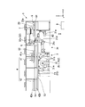
- FIG. 1 is a plan view showing a schematic configuration of a film bonding system 1 of the present embodiment.
- Drawing 2 is a side view showing a schematic structure of film pasting system 1 of this embodiment.
- the transport direction of the liquid crystal panel that is an optical display component is the X direction, and is orthogonal to the X direction in the plane of the liquid crystal panel.
- the direction (width direction of the liquid crystal panel) to be used is the Y direction, and the direction orthogonal to the X direction and the Y direction is the Z direction.
- a film laminating system (optical display device production system) 1 includes a laminating system including a laminating device 3 and the like, a turning reversing device 4, a roller conveyor (first moving device) 5, a second moving device 6, and a detecting device 7.
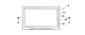
- FIG. 3 is a plan view of the liquid crystal panel P viewed from the thickness direction of the liquid crystal layer P3 of the liquid crystal panel P.
- the liquid crystal panel P includes a first substrate P1 having a rectangular shape in plan view, a second substrate P2 having a relatively small rectangular shape disposed to face the first substrate P1, and A liquid crystal layer P3 enclosed between the first substrate P1 and the second substrate P2 is provided.
- the liquid crystal panel P has a rectangular shape that follows the outer peripheral shape of the first substrate P1 in a plan view, and has a display region P4 that is an area that fits inside the outer periphery of the liquid crystal layer P3 in a plan view.
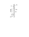
- FIG. 4 is a cross-sectional view taken along the line AA in FIG. As shown in FIG. 4, on the front surface (first surface) of the liquid crystal panel P and on the back surface (second surface) of the liquid crystal panel P, a long strip-shaped first optical member sheet F1 and a long strip-shaped second optical member.
- a first optical member F11 and a second optical member F12 (hereinafter, collectively referred to as an optical member F1X, respectively) cut out from the sheet F2 (see FIG. 1, hereinafter, sometimes collectively referred to as an optical member sheet FX). Is appropriately bonded.
- the first optical member F11 as the polarizing film and the polarizing film are provided on the backlight side surface (first surface) of the liquid crystal panel P and the display surface side surface (second surface) of the liquid crystal panel P.
- Each of the second optical members F12 is bonded.
- a frame portion G having a predetermined width for arranging a sealant or the like for joining the first substrate P1 of the liquid crystal panel P and the second substrate P2 of the liquid crystal panel P is provided outside the display area P4.
- FIG. 5 is a partial cross-sectional view of the optical member sheet FX bonded to the liquid crystal panel P.
- the optical member sheet FX includes a film-like optical member main body F1a, an adhesive layer F2a provided on the first surface (upper surface in FIG. 5) of the optical member main body F1a, and an adhesive layer F2a.
- the separator F3a is detachably stacked on the first surface of the optical member body F1a, and the surface protection film F4a is stacked on the second surface (lower surface in FIG. 5) of the optical member body F1a.
- the optical member main body F1a functions as a polarizing plate, and is bonded over the entire display area P4 of the liquid crystal panel P and the peripheral area of the display area P4. For convenience of illustration, hatching of each layer in FIG. 5 is omitted.
- the optical member main body F1a is bonded to the liquid crystal panel P via the adhesive layer F2a in a state where the separator F3a is separated while leaving the adhesive layer F2a on the first surface of the optical member main body F1a.
- seat FX is called the bonding sheet
- the separator F3a protects the adhesive layer F2a and the optical member body F1a before being separated from the adhesive layer F2a.
- the surface protective film F4a is bonded to the liquid crystal panel P together with the optical member body F1a.
- the surface protective film F4a is disposed on the side opposite to the liquid crystal panel P with respect to the optical member body F1a to protect the optical member body F1a.
- the surface protective film F4a is separated from the optical member main body F1a at a predetermined timing.
- the optical member sheet FX may not include the surface protective film F4a.
- separated from the optical member main body F1a may be sufficient as the surface protection film F4a.
- the optical member body F1a is bonded to the sheet-like polarizer F6, the first film F7 bonded to the first surface of the polarizer F6 with an adhesive or the like, and the second surface of the polarizer F6 with an adhesive or the like. And a second film F8.
- the first film F7 and the second film F8 are protective films that protect the polarizer F6, for example.
- the optical member body F1a may have a single-layer structure composed of a single optical layer, or may have a stacked structure in which a plurality of optical layers are stacked on each other.
- the optical layer may be a retardation film, a brightness enhancement film, or the like.
- At least one of the first film F7 and the second film F8 may be subjected to a surface treatment capable of obtaining an effect such as a hard coat treatment for protecting the outermost surface of the liquid crystal display element or an antiglare treatment.
- the optical member body F1a may not include at least one of the first film F7 and the second film F8.
- the separator F3a may be bonded to the first surface of the optical member body F1a via the adhesive layer F2a.
- the film bonding system 1 of this embodiment is the conveyance direction downstream of the liquid crystal panel P of the left side in a figure from the conveyance direction upstream (+ X direction side) of the liquid crystal panel P of the right side in the figure.
- Drive roller conveyor 5 (first conveyor 51, second conveyor 52, third conveyor 53, and fourth conveyor 54) that reaches the side ( ⁇ X direction side) and conveys the liquid crystal panel P in a horizontal state.
- the roller conveyor 5 corresponds to a first moving device.
- Each of the first conveyor 51, the second conveyor 52, the third conveyor 53, and the fourth conveyor 54 is configured to be able to switch the transport direction of the liquid crystal panel P between the ⁇ X direction and the + X direction.
- the liquid crystal panel P is transported in both the + X direction and the ⁇ X direction, but the liquid crystal panel P is carried in from the end on the + X direction side of the roller conveyor 5 and is carried out from the end on the ⁇ X direction side.
- the + X direction side is referred to as “panel transport upstream side” in the roller conveyor (first moving device) 5
- the ⁇ X direction side is referred to as “panel transport downstream side” in the roller conveyor (first moving device) 5. It will be called “side”.
- the film bonding system 1 of the present embodiment includes a supply device 2, a bonding device 3, a turning reversing device 4, a detection device 7, a second moving device 6, and a storage unit (first storage unit 10, second storage unit 11).
- a transport carriage 8 and a control device 9 are provided.
- the supply device 2 sucks the liquid crystal panel P conveyed on the first conveyor 51 and supplies it to the bonding device 3.
- the supply device 2 includes a panel holding unit 20.
- the panel holding unit 20 holds the liquid crystal panel P so as to be movable in the vertical and horizontal directions and aligns the liquid crystal panel P.
- the panel holding unit 20 sucks and holds the upper surface of the liquid crystal panel P by vacuum suction.
- the panel holding unit 20 moves in a state where the liquid crystal panel P is sucked and held by the suction pad 20a and transports the liquid crystal panel P.
- the panel holding unit 20 releases the suction holding when the conveyance is finished.
- the liquid crystal panel P On the first conveyor 51, the liquid crystal panel P is transported so that the short side of the display area P4 is along the transport direction.
- the supply device 2 may perform alignment (positioning) of the liquid crystal panel P.
- the panel holding unit 20 is provided with an alignment camera.
- the panel holding unit 20 holds the liquid crystal panel P, and images an alignment mark, a tip shape, and the like of the liquid crystal panel P in a raised state.
- Imaging data from the alignment camera is transmitted to the control device 9, and based on this imaging data, the panel holding unit 20 is operated to align the liquid crystal panel P with respect to the bonding apparatus 3 (clamping roll 32) at the transport destination.
- the liquid crystal panel P is conveyed to the bonding apparatus 3 in a state in which the amount of deviation in the conveying direction with respect to the bonding apparatus 3, the direction orthogonal to the conveying direction, and the turning direction around the vertical axis of the liquid crystal panel P is taken into account. .
- the pasting device 3 is provided on the downstream side of the panel transport from the supply device 2.
- the bonding apparatus 3 bonds the sheet piece (optical member F1X) of the bonding sheet F5 cut into a predetermined size on the lower surface of the liquid crystal panel P introduced into the bonding position Q.
- the bonding apparatus 3 includes a transport device 31 and a pinching roll 32.
- the conveying device 31 conveys the optical member sheet FX along the longitudinal direction of the optical member sheet FX while unwinding the optical member sheet FX from the original roll R1 around which the optical member sheet FX is wound.
- the conveyance apparatus 31 conveys the bonding sheet
- the conveyance device 31 includes a roll holding unit 31a, a plurality of guide rollers 31b, a cutting device 31c, a knife edge 31d, and a winding unit 31e.
- the roll holding unit 31a holds the original roll R1 around which the belt-shaped optical member sheet FX is wound and feeds the optical member sheet FX along the longitudinal direction of the optical member sheet FX.
- the plurality of guide rollers 31b wind the optical member sheet FX so as to guide the optical member sheet FX unwound from the original fabric roll R1 along a predetermined conveyance path.
- the cutting device 31c performs a half cut on the optical member sheet FX on the transport path.
- the knife edge 31d supplies the bonding sheet F5 to the bonding position Q while winding the optical member sheet FX subjected to the half cut at an acute angle to separate the bonding sheet F5 from the separator F3a.
- the winding unit 31e holds a separator roll R2 that winds up the separator F3a that has become independent through the knife edge 31d.
- the roll holding unit 31a positioned at the start point of the transport device 31 and the winding unit 31e positioned at the end point of the transport device 31 are driven in synchronization with each other, for example.
- the winding part 31e winds up the separator F3a which passed through the knife edge 31d, while the roll holding part 31a feeds the optical member sheet FX in the transport direction of the optical member sheet FX.
- the upstream side in the transport direction of the optical member sheet FX (separator F3a) in the transport device 31 is referred to as a sheet transport upstream side
- the downstream side in the transport direction is referred to as a sheet transport downstream side.
- Each guide roller 31b changes the traveling direction of the optical member sheet FX being conveyed along the conveyance path, and at least a part of the plurality of guide rollers 31b adjusts the tension of the optical member sheet FX being conveyed. Move.
- a dancer roller (not shown) may be disposed between the roll holding unit 31a and the cutting device 31c.
- the dancer roller absorbs the feeding amount of the optical member sheet FX conveyed from the roll holding unit 31a while the optical member sheet FX is cut by the cutting device 31c. In other words, the dancer roller adjusts the feeding amount of the optical member sheet FX to the cutting device 31c.
- FIG. 6 is a diagram illustrating the operation of the cutting device 31c of the present embodiment.
- the cutting device 31c when the optical member sheet FX is fed out by a predetermined length, the cutting device 31c extends in the thickness direction of the optical member sheet FX over the entire width in the width direction orthogonal to the longitudinal direction of the optical member sheet FX. Perform half cut to cut a part.
- the cutting device 31c of this embodiment is provided so as to be able to advance and retreat from the side opposite to the separator F3a with respect to the optical member sheet FX toward the optical member sheet FX.
- the cutting device 31c adjusts the advancing / retreating position of the cutting blade so that the optical member sheet FX (separator F3a) is not broken by the tension acting during conveyance of the optical member sheet FX (so that a predetermined thickness remains in the separator F3a). Then, half-cut is performed to the vicinity of the interface between the adhesive layer F2 and the separator F3a. In addition, you may use the laser apparatus replaced with a cutting blade.
- the optical member sheet FX after half-cutting is cut along the entire width in the width direction of the optical member sheet FX by cutting the optical member body F1a and the surface protection film F4a in the thickness direction of the optical member sheet FX.
- L2 are formed.
- the cut lines L1 and L2 are formed so as to be aligned in the longitudinal direction of the belt-shaped optical member sheet FX.
- the plurality of cut lines L1 and L2 are formed at equal intervals in the longitudinal direction of the optical member sheet FX.
- the optical member sheet FX is divided into a plurality of sections in the longitudinal direction by a plurality of cut lines L1, L2.
- the sections sandwiched between the pair of cut lines L1 and L2 adjacent in the longitudinal direction in the optical member sheet FX are each one sheet piece (optical member F1X) in the bonding sheet F5.
- the knife edge 31d is arranged below the first conveyor 51 and extends at least over the entire width of the optical member sheet FX in the width direction of the optical member sheet FX.
- the knife edge 31d winds the optical member sheet FX so as to be in sliding contact with the separator F3a of the optical member sheet FX after the half cut.
- the knife edge 31d winds the optical member sheet FX at an acute angle around the tip of the knife edge 31d.
- the sheet piece (optical member F1X) of the bonding sheet F5 is separated from the separator F3a.
- the tip end of the knife edge 31d is disposed close to the panel conveyance downstream side of the pinching roll 32.
- the optical member F1X separated from the separator F3a by the knife edge 31d is introduced between the pair of bonding rollers 32a of the pinching roll 32 while overlapping the lower surface of the liquid crystal panel P.
- the separator F3a separated from the bonding sheet F5 is directed to the winding portion 31e by the knife edge 31d.
- the winding unit 31e winds and collects the separator F3a separated from the bonding sheet F5.
- the pinching roll 32 bonds the optical member F1X separated from the first optical member sheet F1 by the conveying device 31 to the lower surface of the liquid crystal panel P supplied by the supply device 2.
- the pinching roll 32 has a pair of bonding rollers 32a and 32a arranged in parallel with each other in the axial direction (the upper bonding roller 32a is movable up and down). A predetermined gap is formed between the pair of bonding rollers 32 a and 32 a, and the inside of this gap is the bonding position Q of the bonding apparatus 3.
- the liquid crystal panel P is conveyed from the + X direction side to the ⁇ X direction side by the supply device 2 toward the bonding position Q. Then, the liquid crystal panel P and the optical member F1X are overlapped and introduced into the gap between the bonding rollers 32a and 32a. The liquid crystal panel P and the optical member F1X are sent out to the second conveyor 52 while being pressed between the pair of bonding rollers 32a.
- the bonding apparatus 3 includes a first raw roll R11 that unwinds the first optical member sheet F1 having a width corresponding to the long side (first side) of the display area of the liquid crystal panel P, and a liquid crystal. It is possible to switch between the second raw roll R12 that unwinds the band-shaped second optical member sheet F2 having a width corresponding to the short side (second side) of the display area of the panel P.
- the bonding apparatus 3 is a first mode for bonding the first optical member sheet F1 to the liquid crystal panel (optical display component) P, and a second mode for bonding the second optical member sheet F2 to the liquid crystal panel (optical display component) P. 2 modes.
- the posture of the liquid crystal panel P in the bonding apparatus 3 is different between the first mode and the second mode. Specifically, the liquid crystal panel P is inverted and the direction is different by 90 ° between the first mode and the second mode.
- the laminating apparatus 3 has a length corresponding to the short side of the display area of the liquid crystal panel (the first optical member sheet F1 unwound from the first original fabric roll R11).
- disconnecting by 2 length) is bonded to the 1st surface of liquid crystal panel P.
- 1st optical member bonding body PA1 optical member bonding body is formed by bonding the 1st optical member F11 to the surface at the side of the backlight of liquid crystal panel P with the pinching roll 32.
- the bonding apparatus 3 has a length corresponding to the long side of the display area of the liquid crystal panel P with respect to the second optical member sheet F2 unwound from the second original fabric roll R12 (The second optical member F12 obtained by cutting at the first length) is bonded to the second surface of the liquid crystal panel P.
- the second optical is applied to the surface on the display surface side of the liquid crystal panel P (the surface opposite to the surface on which the first optical member F11 of the first optical member bonding body PA1 is bonded) by the pinching roll 32.
- the second optical member bonding body PA2 optical display device
- the length of the first side (first length) of the display area of the liquid crystal panel P is substantially the same as the length of the second side (second length) orthogonal to the first side. Also good.
- the bonding apparatus 3 includes a first raw roll R11 that unwinds the first optical member sheet F1 having a width corresponding to the short side of the display area of the liquid crystal panel P, and the long side of the display area of the liquid crystal panel P. And a second raw roll R12 that unwinds the band-shaped second optical member sheet F2 having a width corresponding to the width of the second optical member sheet F2.
- the bonding apparatus 3 uses the first optical member sheet F1 unwound from the first original fabric roll R11 to the length corresponding to the long side of the display area of the liquid crystal panel.
- the first optical member F11 obtained by cutting is bonded to the first surface of the liquid crystal panel P.
- the laminating apparatus 3 sets the second optical member sheet F2 unwound from the second original fabric roll R12 to a length corresponding to the short side of the display area of the liquid crystal panel P.
- the second optical member F12 obtained by cutting is bonded to the second surface of the liquid crystal panel P.
- the turning reversing device 4 is provided on the downstream side of the panel conveyance from the bonding device 3.
- the turning reversing device 4 turns (rotates) and reverses (turns over) the first optical member bonding body PA1.
- the turning reversing device 4 includes a turning device (turning mechanism) 41 and a reversing device (reversing mechanism) 42.
- the swivel device 41 is arranged above the second conveyor 52 (on the + Z direction side).
- the turning device 41 turns the first optical member bonding body PA1 and the second optical member bonding body PA2 in a turning direction around the vertical axis of the liquid crystal panel P in a state where the first optical member bonding body PA1 and the second optical member bonding body PA2 are adsorbed to the suction pad 41a.
- the turning device 41 is configured to change the direction (angular position around a predetermined axis) of the liquid crystal panel P to which at least one of the first optical member F11 and the second optical member F12 is bonded.
- each of the turning device 41 and the second conveyor 52 includes a conveying direction (X direction) with respect to the roller conveyor 5, a direction orthogonal to the conveying direction (Y direction), and a turning direction around the vertical axis of the liquid crystal panel P. It is configured to be movable.
- the second conveyor 52 is, for example, a cross conveyor.
- only the turning device 41 is configured to be movable in the turning direction around the vertical axis of the liquid crystal panel P, and only the second conveyor 52 is in the conveying direction (X direction) with respect to the roller conveyor 5 and in the direction orthogonal to the conveying direction ( (Y direction) may be configured to be movable.
- the reversing device 42 is provided on the downstream side of the panel transport with respect to the turning device 41.
- the reversing device 42 is turned over by sandwiching the first optical member bonding body PA1 and the second optical member bonding body PA2 conveyed on the fourth conveyor 54 from above and below with a pair of support materials 42a and 42b.
- the front and back of the bonding body PA1 and the second optical member bonding body PA2 are reversed.
- the turning reversing device 4 may not include the turning device 41 and the reversing device 42 separately.
- the turning reversing device 4 includes a reversing mechanism having a reversing axis that makes an oblique 45 ° with respect to the transport direction (X direction) of the liquid crystal panel P, thereby realizing a swiveling function and a reversing function with a single reversing operation It may be a turning reversing device. In this case, since both the turning process and the reversing process are performed by the reversing mechanism, it is not necessary to provide a turning device separately.
- the roller conveyor 5 moves the first optical member bonding body PA1 from the bonding device 3 to the turning and reversing device 4 and bonds the second optical member F12 to the surface on the display surface side of the liquid crystal panel P.
- the 1st optical member bonding body PA1 rotated and reversed by the turning inversion apparatus 4 is moved from the turning inversion apparatus 4 to the bonding apparatus 3.
- the detection device 7 is provided between the turning device 41 and the reversing device 42.
- the detection device 7 detects the relative bonding position of the optical member F1X with respect to the liquid crystal panel P.
- the detection device 7 determines whether or not the position of the optical member F1X is appropriate in the work (liquid crystal panel P) on which the film is bonded (whether or not the positional deviation is within the tolerance range).
- the detecting device 7 has a plurality of cameras 7a arranged in a direction (Y direction) orthogonal to the panel transport direction.
- the plurality of cameras 7a are arranged above the third conveyor 53 (on the + Z direction side).
- the camera 7a captures an image including the edge of the optical member F1X in the liquid crystal panel P.
- Imaging data from the camera 7a is transmitted to the control device 9, and based on this imaging data, it is determined whether or not the bonding position of the optical member F1X on the liquid crystal panel P is appropriate.
- the work determined that the position of the optical member F1X with respect to the liquid crystal panel P is not appropriate is discharged out of the line by a not-shown discharging means.
- the second moving device 6 is provided at a position adjacent to the turning device 41 (second conveyor 52) in a direction (+ Y direction) orthogonal to the panel conveying direction (X direction) in the roller conveyor (first moving device) 5. Yes.
- the second moving device 6 moves the first optical member bonding body PA1 from the turning and reversing device 4 to the storage unit (first storage unit 10, second storage unit 11) and the storage unit (first storage unit 10, first storage unit 10).
- the first optical member bonding body PA1 is moved from the second storage portion 11) to the turning and reversing device 4.
- the storage units (the first storage unit 10 and the second storage unit 11) temporarily store the liquid crystal panel P (for example, the liquid crystal panel P on which at least one of the first optical member F11 and the second optical member F12 is bonded).
- the turning device (turning mechanism) 41 includes (a) a bonding device 3 and a storage unit (first storage unit 10, second storage unit 11), and (b) a reversing device (reversing mechanism) 42. And the storage unit (the first storage unit 10 and the second storage unit 11) are disposed on at least one transport path of the liquid crystal panel P.
- 1st optical member bonding body PA1 Before the 1st optical member bonding body PA1 is moved to the accommodating part (the 1st accommodating part 10 and the 2nd accommodating part 11) by the 2nd moving apparatus 6, it is liquid crystal panel by the turning inversion apparatus 4 (the turning apparatus 41). It is turned 90 ° in the turning direction around the vertical axis of P. Thereby, 1st optical member bonding body PA1 becomes the attitude
- the second moving device 6 includes a conveyor 61 and a transfer machine 62.
- the conveyor 61 is provided at a position adjacent to the turning device 41 (second conveyor 52) in a direction (+ Y direction) orthogonal to the panel conveying direction in the roller conveyor (first moving device) 5.
- the conveyor 61 moves the first optical member bonding body PA1 from the turning reversing device 4 to the transfer device 62 and moves the first optical member bonding body PA1 from the transfer device 62 to the turning reversing device 4.
- the transfer device 62 is provided so as to be movable between the conveyor 61 and the storage units (the first storage unit 10 and the second storage unit 11).
- the transfer device 62 moves the first optical member bonding body PA1 from the conveyor 61 to the storage units (the first storage unit 10 and the second storage unit 11) and also transfers the first optical member from the storage units 10 and 11 to the conveyor 61.
- the bonded body PA1 is moved.
- the first storage unit 10 and the second storage unit 11 are provided at positions adjacent to the roller conveyor 5 in the Y direction.
- the first storage unit 10 and the second storage unit 11 are arranged to face each other with the conveyor 61 interposed therebetween.
- Each of the first storage unit 10 and the second storage unit 11 stores a predetermined number (for example, 50) of the first optical member bonding body PA1.
- the transport carriage 8 is arranged at a position adjacent to the roller conveyor 5.
- the conveyance carriage 8 conveys the raw fabric roll R1 to the bonding apparatus 3 for paper joining.
- the original fabric roll R1 stands by at a position adjacent to the laminating device 3 for paper splicing.
- the transport carriage 8 has a roll support portion 8a that supports the raw fabric roll R1.
- the transport carriage 8 is provided so as to be capable of reciprocating between a roll accommodation area (not shown) in which a plurality of raw fabric rolls R1 are stocked and the laminating apparatus 3.
- a tracked or magnetic induction type unmanned transport truck AGV: automated guided vehicle
- the control apparatus 9 as an electronic control apparatus which performs overall control of each part of the film bonding system 1 includes a computer system.
- This computer system includes an arithmetic processing unit such as a CPU and a storage unit such as a memory and a hard disk.
- the control device 9 of the present embodiment includes an interface capable of executing communication with a device external to the computer system.
- An input device that can input an input signal may be connected to the control device 9.
- the input device includes an input device such as a keyboard and a mouse, or a communication device that can input data from a device external to the computer system.
- the control device 9 may include a display device such as a liquid crystal display that indicates the operation status of each part of the film bonding system 1.
- the control device 9 may be connected to a display device.
- An operating system (OS) that controls the computer system is installed in the storage unit of the control device 9.
- a program that causes the storage unit of the control device 9 to execute processing for causing each unit of the film bonding system 1 to accurately convey the optical member sheet FX by causing the arithmetic processing unit to control each unit of the film bonding system 1. Is recorded.
- Various types of information including programs recorded in the storage unit can be read by the arithmetic processing unit of the control device 9.
- the control device 9 may include a logic circuit such as an ASIC that executes various processes required for controlling each part of the film bonding system 1.
- the storage unit includes a semiconductor memory such as a RAM (Random Access Memory) and a ROM (Read Only Memory), an external storage device such as a hard disk, a CD-ROM reader, and a disk-type storage medium.
- the storage unit is a supply device 2, a bonding device 3, a turning reversal device 4, a detection device 7, a second moving device 6, a storage unit (first storage unit 10, second storage unit 11), and conveyance
- FIG. 7 is a diagram showing an operation flow of the film bonding system.
- the movement by the roller conveyor 5 is indicated as “first movement”
- the movement by the second movement device 6 is indicated as “second movement”.
- the liquid crystal panel P is conveyed on the first conveyor 51, and is supplied to the bonding apparatus 3 by the supply apparatus 2 (step S1 shown in FIG. 7).
- the liquid crystal panel P is moved in the ⁇ X direction by the first conveyor 51 toward the bonding position Q so that the short side of the display area P4 is along the transport direction.
- the length of the roller conveyor 5 (first conveyor 51) in the panel transport direction (X direction) can be shortened. . This facilitates downsizing of the device.
- the liquid crystal panel P may be moved so that the long side of the display area P4 is along the transport direction.
- the liquid crystal panel P is moved so that the short side of the display region P4 is along the transport direction.
- Step S2 bonding of the sheet piece (first optical member F11) of the bonding sheet F5 cut into a predetermined size is performed on the lower surface of the liquid crystal panel P introduced into the bonding position Q by the bonding apparatus 3.
- 1st optical member bonding body PA1 is formed.
- the first optical member bonding body PA1 is moved in the ⁇ X direction toward the detection device 7 by the second conveyor 52 (step S3 shown in FIG. 7).
- step S4 the relative bonding position of the first optical member F11 with respect to the liquid crystal panel P is detected by the detection device 7 (step S4 shown in FIG. 7).
- the 1st optical member bonding body PA1 determined that the bonding position of the 1st optical member F11 in liquid crystal panel P is appropriate is moved to the inversion apparatus 42 by the 3rd conveyor 53 to -X direction.
- the first optical member bonding body PA1 with the display surface side of the liquid crystal panel P on the top surface is reversed by the reversing device 42 so that the backlight side of the liquid crystal panel P is on the top surface (step S5 shown in FIG. 7).
- 1st optical member bonding body PA1 by which the backlight side of liquid crystal panel P was made into the upper surface is moved to + X direction toward the turning apparatus 41 by the 4th conveyor 54 and the 3rd conveyor 53.
- the first optical member bonding body PA1 is turned 90 ° in the turning direction around the vertical axis of the liquid crystal panel P by the turning device 41 (step S6 shown in FIG. 7).
- 1st optical member bonding body PA1 becomes the attitude
- FIG. 1 since the 2nd conveyor 52 is also comprised so that turning is possible, you may perform the turning process of 1st optical member bonding body PA1 with the 2nd conveyor 52.
- FIG. 1 since the 2nd conveyor 52 is also comprised so that turning is possible, you may perform the turning process of 1st optical member bonding body PA1 with the 2nd conveyor 52.
- Step S7 shown in FIG. 7).
- the movement process of 1st optical member bonding body PA1 is not restricted to performing with the 2nd conveyor 52.
- the turning device 41 since the turning device 41 is also configured to be movable in the Y direction, the turning process of the first optical member bonding body PA1 may be performed by the turning device 41.
- the 1st optical member bonding body PA1 is accommodated in the 1st accommodating part 10 or the 2nd accommodating part 11 by the transfer machine 62 (step S8 shown in FIG. 7).
- the storage method by the transfer machine 62 is as follows. First, the first optical member bonding body PA1 is stored only in the first storage portion 10, and the first optical member bonding body PA1 is filled when the first storage portion 10 is full. You may employ
- the raw roll R1 is switched by the bonding device 3 and the transport carriage 8 (step shown in FIG. 7). S9).
- the 1st original fabric roll R11 currently loaded in the bonding apparatus 3 is switched to the 2nd original fabric roll R12, and the bonding apparatus 3 is made to load the 2nd original fabric roll R12.
- the first optical member bonding body PA1 is taken out from the first storage unit 10 or the second storage unit 11 by the transfer device 62 (step S10 shown in FIG. 7).
- the take-out method by the transfer device 62 is such that the first optical member bonding body PA1 is first taken out only from the first storage unit 10 and the first storage unit 10 is emptied.
- the taken out first optical member bonding body PA1 is moved toward the conveyor 61 by the transfer device 62.
- the movement process of 1st optical member bonding body PA1 is not restricted to performing with the conveyor 61.
- the first optical member bonding body PA1 is moved in the + X direction toward the first conveyor 51 so that the long side of the display region P4 is along the transport direction (X direction) (FIG. Step S12 shown in FIG.
- the first conveyor 51 is moved in the ⁇ X direction toward the bonding position Q so that the long side of the display region P4 is along the transport direction, and is supplied to the bonding device 3 by the supply device 2.
- Step S13 bonding of the sheet piece (second optical member F12) of the bonding sheet F5 cut into a predetermined size is performed on the lower surface of the liquid crystal panel P introduced into the bonding position Q by the bonding apparatus 3.
- 2nd optical member bonding body PA2 by which the polarizing axes (optical axis) of a pair of polarizing film were mutually orthogonally arrange
- positioned cross Nicol arrangement
- the second optical member bonding body PA2 is conveyed to the turning reversing device 4 and turned 90 ° in the turning direction around the vertical axis of the liquid crystal panel P by the turning device 41 (step S14 shown in FIG. 7). Thereafter, the second optical member bonding body PA2 is moved in the ⁇ X direction toward the detection device 7 by the second conveyor 52.
- step S15 the relative bonding position of the second optical member F12 with respect to the liquid crystal panel P is detected by the detection device 7 (step S15 shown in FIG. 7).
- the short direction (short side of a display area) of 1st optical member bonding body PA1 and 2nd optical member bonding body PA2 is carried out before the detection of the relative bonding position by the detection apparatus 7, the short direction (short side of a display area) of 1st optical member bonding body PA1 and 2nd optical member bonding body PA2 is carried out.
- a conveyance direction (X direction) it is not restricted to this,
- the longitudinal direction (long side of a display field) of 1st optical member bonding body PA1 and 2nd optical member bonding body PA2 is the conveyance direction (X direction).
- the bonding apparatus 3, the turning inversion apparatus 4, and the detection apparatus 7 are about 1st optical member bonding body PA1 and 2nd optical member bonding body PA2. Shared. Therefore, the downsizing and cost reduction of the equipment can be realized.
- the bonding of the 1st optical member F11 and the 2nd optical member F12 is performed with the one bonding apparatus 3, the time of the raw material replacement
- the first optical member bonding body PA1 is sequentially taken out from the storage units (first storage unit 10 and second storage unit 11), and the bonding process of the second optical member F12 is performed by the bonding device 3. Therefore, such a decrease in production efficiency can be minimized.
- the bonding apparatus 3 once bonds the optical member peeled from the separator to a bonding portion such as a bonding head or a bonding drum that is a transfer body, and aligns the bonding portion with respect to the liquid crystal panel P. And the optical member stuck by the bonding part may be bonded to a liquid crystal panel.
- the film bonding system 1 (production system for an optical display device) according to an embodiment of the present invention is bonded to the liquid crystal panel P (optical display component) and the surface (first surface) of the liquid crystal panel P.
- This is a system for producing a liquid crystal display device (optical display device) having a combined first optical member F11 and a second optical member F12 bonded to the back surface (second surface) of the liquid crystal panel P.
- the film bonding system 1 includes a bonding device 3 for bonding the optical member F1X to the liquid crystal panel P, a turning reversing device 4 for turning and reversing the liquid crystal panel P, and a bonding device 3 and a turning reversing device 4.
- a roller conveyor 5 for moving the liquid crystal panel P and a control device 9 (control unit).
- the control device 9 (a) controls the bonding device 3 to bond the first optical member F11 to the surface of the liquid crystal panel P to form a first optical member bonding body PA1 (optical member bonding body).
- roller conveyor 5 is controlled to move the first optical member bonding body PA1 swung and reversed by the turning reversing device 4 from the turning reversing device 4 to the bonding device 3, and (e) pasting
- the combination device 3 is controlled to bond the second optical member F12 to the back surface of the liquid crystal panel P.
- SYMBOLS 1 Film bonding system (production system of an optical display device), 3 ... Bonding apparatus, 4 ... Turning inversion apparatus, 5 ... Roller conveyor (1st moving apparatus), 6 ... Second moving apparatus, 7 ... Detection apparatus, 41 ... turning device, 42 ... reversing device, F11 ... first optical member, F12 ... second optical member, F1X ... optical member, PA1 ... first optical member bonding body, PA2 ... second optical member bonding body, R11 ... first One original roll, R12 ... Second original roll.
Landscapes
- Physics & Mathematics (AREA)
- Nonlinear Science (AREA)
- General Physics & Mathematics (AREA)
- Optics & Photonics (AREA)
- Crystallography & Structural Chemistry (AREA)
- Chemical & Material Sciences (AREA)
- Mathematical Physics (AREA)
- Engineering & Computer Science (AREA)
- Manufacturing & Machinery (AREA)
- Liquid Crystal (AREA)
- Fluid Mechanics (AREA)
- Devices For Indicating Variable Information By Combining Individual Elements (AREA)
- Polarising Elements (AREA)
- Theoretical Computer Science (AREA)
Abstract
Description
本願は、2013年8月8日に出願された日本国特許出願2013-165501号に基づき優先権を主張し、その内容をここに援用する。
(1)本発明の第一の態様に係る光学表示デバイスの生産システムは、光学表示部品の第1面に第一光学部材を貼合し、前記光学表示部品の第2面に第二光学部材を貼合して形成される光学表示デバイスの生産システムであって、前記光学表示部品の前記第1面に前記第一光学部材を貼合して光学部材貼合体を形成する貼合装置と、前記光学部材貼合体を旋回及び反転させる旋回反転装置と、前記貼合装置から前記旋回反転装置に前記光学部材貼合体を移動させるとともに、前記光学表示部品の前記第2面に前記第二光学部材を貼合するために、前記旋回反転装置によって旋回及び反転された前記光学部材貼合体を前記旋回反転装置から前記貼合装置に移動させる第一移動装置と、を含む。
尚、以下の全ての図面においては、図面を見やすくするため、各構成要素の寸法や比率などは適宜異ならせてある。また、以下の説明及び図面中、同一又は相当する要素には同一の符号を付し、重複する説明は省略する。
本実施形態では、光学表示デバイスの生産システムとして、その一部を構成するフィルム貼合システムについて説明する。フィルム貼合システムは、例えば液晶パネルや有機ELパネルといったパネル状の光学表示部品に、偏光フィルムや反射防止フィルム、光拡散フィルムといったフィルム状の光学部材を貼合するシステムである。本実施形態では、一例として、液晶パネル(光学表示部品)の両面に偏光フィルム(光学部材)がそれぞれ貼合されることにより液晶表示装置(光学表示デバイス)が生産される構成を挙げて説明する。
図3に示すように、液晶パネルPは、平面視で長方形状を有する第1基板P1と、第1基板P1に対向して配置される比較的小形の長方形状を有する第2基板P2と、第1基板P1と第2基板P2との間に封入された液晶層P3とを備える。液晶パネルPは、平面視で第1基板P1の外周形状に沿う長方形状を有し、平面視で液晶層P3の外周の内側に収まる領域である表示領域P4を有する。
図4に示すように、液晶パネルPの表面(第1面)及び液晶パネルPの裏面(第2面)には、長尺帯状の第一光学部材シートF1及び長尺帯状の第二光学部材シートF2(図1参照、以下、光学部材シートFXと総称することがある。)からそれぞれ切り出した第一光学部材F11及び第二光学部材F12(以下、光学部材F1Xと総称することがある。)が適宜貼合される。本実施形態では、液晶パネルPのバックライト側の面(第1面)及び液晶パネルPの表示面側の面(第2面)には、偏光フィルムとしての第一光学部材F11及び偏光フィルムとしての第二光学部材F12がそれぞれ貼合される。
図5に示すように、光学部材シートFXは、フィルム状の光学部材本体F1aと、光学部材本体F1aの第1面(図5では上面)に設けられた粘着層F2aと、粘着層F2aを介して光学部材本体F1aの第1面に分離可能に積層されたセパレータF3aと、光学部材本体F1aの第2面(図5では下面)に積層された表面保護フィルムF4aとを有する。光学部材本体F1aは偏光板として機能し、液晶パネルPの表示領域P4の全域と表示領域P4の周辺領域とにわたって貼合される。尚、図示都合上、図5の各層のハッチングは省略する。
図1及び図2に示すように、本実施形態のフィルム貼合システム1は、図中右側の液晶パネルPの搬送方向上流側(+X方向側)から図中左側の液晶パネルPの搬送方向下流側(-X方向側)に至り、液晶パネルPを水平状態で搬送する駆動式のローラコンベア5(第一コンベア51、第二コンベア52、第三コンベア53及び第四コンベア54)を備えている。ここで、ローラコンベア5は、第一移動装置に相当する。
搬送装置31は、光学部材シートFXが巻回された原反ロールR1から光学部材シートFXを巻き出しつつ光学部材シートFXの長手方向に沿って光学部材シートFXを搬送する。搬送装置31は、セパレータF3aをキャリアとして貼合シートF5を搬送する。
搬送装置31は、ロール保持部31aと、複数のガイドローラ31bと、切断装置31cと、ナイフエッジ31dと、巻き取り部31eと、を備えている。
複数のガイドローラ31bは、原反ロールR1から巻き出した光学部材シートFXを所定の搬送経路に沿って案内するように光学部材シートFXを巻きかける。
切断装置31cは、搬送経路上の光学部材シートFXにハーフカットを施す。
ナイフエッジ31dは、ハーフカットを施した光学部材シートFXを鋭角に巻きかけてセパレータF3aから貼合シートF5を分離させつつ貼合シートF5を貼合位置Qに供給する。
巻き取り部31eは、ナイフエッジ31dを経て単独となったセパレータF3aを巻き取るセパレータロールR2を保持する。
図6に示すように、切断装置31cは、光学部材シートFXが所定長さ繰り出された際、光学部材シートFXの長手方向と直交する幅方向の全幅にわたって、光学部材シートFXの厚さ方向の一部を切断するハーフカットを行う。本実施形態の切断装置31cは、光学部材シートFXに対してセパレータF3aとは反対側から光学部材シートFXに向かって進退可能に設けられている。
この場合、第一原反ロールR11の装填時において、貼合装置3は、第一原反ロールR11から巻き出された第一光学部材シートF1を液晶パネルの表示領域の長辺に対応する長さで切断して得られた第一光学部材F11を液晶パネルPの第1面に貼合する。
一方、第二原反ロールR12の装填時において、貼合装置3は、第二原反ロールR12から巻き出された第二光学部材シートF2を液晶パネルPの表示領域の短辺に対応する長さで切断して得られた第二光学部材F12を液晶パネルPの第2面に貼合する。
旋回装置41は、第二コンベア52の上方(+Z方向側)に配置されている。旋回装置41は、第一光学部材貼合体PA1及び第二光学部材貼合体PA2を、吸着パッド41aに吸着した状態で、液晶パネルPの垂直軸回りの旋回方向で旋回させる。旋回装置41は、第一光学部材F11及び第二光学部材F12の少なくとも1つが貼合された液晶パネルPの向き(所定軸周りの角度位置)を変えるように構成されている。
コンベア61は、ローラコンベア(第一移動装置)5におけるパネル搬送方向と直交する方向(+Y方向)において旋回装置41(第二コンベア52)と隣り合う位置に設けられている。コンベア61は、旋回反転装置4から移載機62に第一光学部材貼合体PA1を移動させるとともに、移載機62から旋回反転装置4に第一光学部材貼合体PA1を移動させる。
移載機62は、コンベア61から収納部(第一収納部10、第二収納部11)に第一光学部材貼合体PA1を移動させるとともに、収納部10,11からコンベア61に第一光学部材貼合体PA1を移動させる。
本実施形態の制御装置9は、コンピュータシステムの外部の装置との通信を実行可能なインターフェースを含む。制御装置9には、入力信号を入力可能な入力装置が接続されていてもよい。上記の入力装置は、キーボード、マウス等の入力機器、あるいはコンピュータシステムの外部の装置からのデータを入力可能な通信装置等を含む。制御装置9は、フィルム貼合システム1の各部の動作状況を示す液晶表示ディスプレイ等の表示装置を含んでいてもよい。制御装置9は、表示装置と接続されていてもよい。
図7は、フィルム貼合システムの動作フローを示す図である。図7においては、便宜上、ローラコンベア5(第一移動装置)による移動を「第一の移動」、第二移動装置6による移動を「第二の移動」として示す。
尚、液晶パネルPは、表示領域P4の長辺を搬送方向に沿うようにして移動されてもよい。ただし、ローラコンベア5(第一コンベア51)のパネル搬送方向(X方向)の長さを短くする観点からは、液晶パネルPは、表示領域P4の短辺を搬送方向に沿うようにして移動される。
フィルム貼合システム1は、液晶パネルPに光学部材F1Xを貼合する貼合装置3と、液晶パネルPを旋回及び反転させる旋回反転装置4と、貼合装置3と旋回反転装置4との間で液晶パネルPを移動させるローラコンベア5(第一移動装置)と、制御装置9(制御部)と、を備える。
制御装置9は、(a)貼合装置3を制御して液晶パネルPの表面に第一光学部材F11を貼合して第一光学部材貼合体PA1(光学部材貼合体)を形成し、(b)ローラコンベア5を制御して貼合装置3から旋回反転装置4に第一光学部材貼合体PA1を移動させ、(c)旋回反転装置4を制御して第一光学部材貼合体PA1を旋回及び反転させ、(d)ローラコンベア5を制御して旋回反転装置4から貼合装置3に、旋回反転装置4によって旋回及び反転された第一光学部材貼合体PA1を移動させ、(e)貼合装置3を制御して液晶パネルPの裏面に第二光学部材F12を貼合する。
Claims (5)
- 光学表示部品の第1面に第一光学部材を貼合し、前記光学表示部品の第2面に第二光学部材を貼合して形成される光学表示デバイスの生産システムであって、
前記光学表示部品の前記第1面に前記第一光学部材を貼合して光学部材貼合体を形成する貼合装置と、
前記光学部材貼合体を旋回及び反転させる旋回反転装置と、
前記貼合装置から前記旋回反転装置に前記光学部材貼合体を移動させるとともに、前記光学表示部品の前記第2面に前記第二光学部材を貼合するために、前記旋回反転装置によって旋回及び反転された前記光学部材貼合体を前記旋回反転装置から前記貼合装置に移動させる第一移動装置と、
を含む光学表示デバイスの生産システム。 - 前記光学部材貼合体を収納する収納部と、
前記旋回反転装置から前記収納部に前記光学部材貼合体を移動させるとともに、前記収納部から前記旋回反転装置に前記光学部材貼合体を移動させる第二移動装置と、
を含む請求項1に記載の光学表示デバイスの生産システム。 - 前記旋回反転装置は、前記光学部材貼合体を旋回させる旋回装置と、前記光学部材貼合体を反転させる反転装置と、を含む請求項1又は2に記載の光学表示デバイスの生産システム。
- 前記旋回反転装置は、前記旋回装置と前記反転装置との間に、前記光学表示部品に対する前記第一光学部材の相対貼合位置及び前記光学表示部品に対する前記第二光学部材の相対貼合位置を検出する検出装置を含む請求項3に記載の光学表示デバイスの生産システム。
- 前記光学表示部品は、第1長さの第1辺と第2長さの第2辺とを有する表示領域を含み、
前記貼合装置は、前記第1長さに対応する幅の帯状の第一光学部材シートを巻き出す第一原反ロールと、前記第2長さに対応する幅の帯状の第二光学部材シートを巻き出す第二原反ロールとを切換え可能であり、
前記貼合装置は、前記第一原反ロールから巻き出された前記第一光学部材シートを前記第2長さに対応する長さで切断して得られた前記第一光学部材を前記光学表示部品の第1面に貼合するとともに、前記第二原反ロールから巻き出された前記第二光学部材シートを前記第1長さに対応する長さで切断して得られた前記第二光学部材を前記光学表示部品の第2面に貼合する請求項1から4までのいずれか一項に記載の光学表示デバイスの生産システム。
Priority Applications (2)
| Application Number | Priority Date | Filing Date | Title |
|---|---|---|---|
| KR1020167003034A KR102162945B1 (ko) | 2013-08-08 | 2014-07-31 | 광학 표시 디바이스의 생산 시스템 |
| CN201480044045.7A CN105453160B (zh) | 2013-08-08 | 2014-07-31 | 光学显示设备的生产系统 |
Applications Claiming Priority (2)
| Application Number | Priority Date | Filing Date | Title |
|---|---|---|---|
| JP2013-165501 | 2013-08-08 | ||
| JP2013165501A JP6178660B2 (ja) | 2013-08-08 | 2013-08-08 | 光学表示デバイスの生産システム |
Publications (1)
| Publication Number | Publication Date |
|---|---|
| WO2015019932A1 true WO2015019932A1 (ja) | 2015-02-12 |
Family
ID=52461268
Family Applications (1)
| Application Number | Title | Priority Date | Filing Date |
|---|---|---|---|
| PCT/JP2014/070188 Ceased WO2015019932A1 (ja) | 2013-08-08 | 2014-07-31 | 光学表示デバイスの生産システム |
Country Status (5)
| Country | Link |
|---|---|
| JP (1) | JP6178660B2 (ja) |
| KR (1) | KR102162945B1 (ja) |
| CN (1) | CN105453160B (ja) |
| TW (1) | TWI643169B (ja) |
| WO (1) | WO2015019932A1 (ja) |
Cited By (1)
| Publication number | Priority date | Publication date | Assignee | Title |
|---|---|---|---|---|
| CN111402720A (zh) * | 2020-04-23 | 2020-07-10 | 深圳市汇凌信息技术有限公司 | 一种屏贴合组件及其高效贴合设备与贴合方法 |
Families Citing this family (1)
| Publication number | Priority date | Publication date | Assignee | Title |
|---|---|---|---|---|
| JP6619762B2 (ja) * | 2017-03-27 | 2019-12-11 | 平田機工株式会社 | 製造システムおよび製造方法 |
Citations (3)
| Publication number | Priority date | Publication date | Assignee | Title |
|---|---|---|---|---|
| JP2009175653A (ja) * | 2007-12-27 | 2009-08-06 | Nitto Denko Corp | 光学表示装置の製造システム及び製造方法 |
| JP2011232383A (ja) * | 2010-04-23 | 2011-11-17 | Sumitomo Chemical Co Ltd | 偏光フィルムの貼合装置およびこれを備える液晶表示装置の製造システム |
| JP2012073425A (ja) * | 2010-09-29 | 2012-04-12 | Nitto Denko Corp | 液晶表示素子の連続製造システムおよび液晶表示素子の連続製造方法 |
Family Cites Families (18)
| Publication number | Priority date | Publication date | Assignee | Title |
|---|---|---|---|---|
| CN100495149C (zh) * | 2006-08-17 | 2009-06-03 | 株式会社爱发科 | 贴合方法及贴合基板制造装置 |
| JP2008139523A (ja) * | 2006-12-01 | 2008-06-19 | Hitachi High-Technologies Corp | 光学フィルム貼付け方法、光学フィルム貼付け装置、及び表示用パネルの製造方法 |
| KR100918854B1 (ko) * | 2007-03-27 | 2009-09-28 | 한동희 | 편광필름 부착장치 |
| JP2009109981A (ja) * | 2007-07-31 | 2009-05-21 | Hitachi High-Technologies Corp | 光学フィルム貼り付け方法、光学フィルム貼り付け装置、及び表示用パネルの製造方法 |
| JP4855493B2 (ja) * | 2008-04-14 | 2012-01-18 | 日東電工株式会社 | 光学表示装置製造システム及び光学表示装置製造方法 |
| JP4669070B2 (ja) | 2009-05-21 | 2011-04-13 | 日東電工株式会社 | 光学表示装置の製造システム及び製造方法 |
| WO2011070820A1 (ja) * | 2009-12-09 | 2011-06-16 | 住友化学株式会社 | 光学表示装置の製造システムおよび当該光学表示装置の製造方法 |
| JP4751997B1 (ja) * | 2010-02-17 | 2011-08-17 | 住友化学株式会社 | 偏光フィルムの貼合装置およびこれを備える液晶表示装置の製造システム |
| JP2011197280A (ja) * | 2010-03-18 | 2011-10-06 | Sumitomo Chemical Co Ltd | 光学フィルム貼合装置及び貼合方法 |
| WO2011122005A1 (ja) * | 2010-03-30 | 2011-10-06 | 住友化学株式会社 | 基板搬送機構および偏光フィルムの貼合装置における反転機構 |
| CN102844702B (zh) * | 2010-04-12 | 2015-07-29 | 住友化学株式会社 | 偏振膜的贴合装置及具有该贴合装置的液晶显示装置的制造系统 |
| WO2011132332A1 (ja) * | 2010-04-23 | 2011-10-27 | 住友化学株式会社 | 偏光フィルムの貼合装置およびこれを備える液晶表示装置の製造システム |
| KR101270699B1 (ko) * | 2010-06-22 | 2013-06-03 | 엘지디스플레이 주식회사 | 액정표시패널 제조장치 |
| JP5167319B2 (ja) * | 2010-09-01 | 2013-03-21 | 日東電工株式会社 | 光学機能フィルム、及びこれを用いた液晶表示装置の製造方法 |
| JP4733227B1 (ja) * | 2010-09-30 | 2011-07-27 | 日東電工株式会社 | 液晶表示素子の製造システム及び製造方法 |
| JP4729647B1 (ja) * | 2010-11-02 | 2011-07-20 | 日東電工株式会社 | 液晶表示素子の製造システム |
| JP5792597B2 (ja) * | 2010-11-25 | 2015-10-14 | 日東電工株式会社 | 液晶表示素子の製造方法および液晶表示素子の製造システム |
| JP5763468B2 (ja) * | 2011-08-09 | 2015-08-12 | 日東電工株式会社 | 液晶表示素子の製造方法および液晶表示素子の製造システム |
-
2013
- 2013-08-08 JP JP2013165501A patent/JP6178660B2/ja active Active
-
2014
- 2014-07-31 WO PCT/JP2014/070188 patent/WO2015019932A1/ja not_active Ceased
- 2014-07-31 CN CN201480044045.7A patent/CN105453160B/zh active Active
- 2014-07-31 KR KR1020167003034A patent/KR102162945B1/ko active Active
- 2014-08-01 TW TW103126408A patent/TWI643169B/zh active
Patent Citations (3)
| Publication number | Priority date | Publication date | Assignee | Title |
|---|---|---|---|---|
| JP2009175653A (ja) * | 2007-12-27 | 2009-08-06 | Nitto Denko Corp | 光学表示装置の製造システム及び製造方法 |
| JP2011232383A (ja) * | 2010-04-23 | 2011-11-17 | Sumitomo Chemical Co Ltd | 偏光フィルムの貼合装置およびこれを備える液晶表示装置の製造システム |
| JP2012073425A (ja) * | 2010-09-29 | 2012-04-12 | Nitto Denko Corp | 液晶表示素子の連続製造システムおよび液晶表示素子の連続製造方法 |
Cited By (1)
| Publication number | Priority date | Publication date | Assignee | Title |
|---|---|---|---|---|
| CN111402720A (zh) * | 2020-04-23 | 2020-07-10 | 深圳市汇凌信息技术有限公司 | 一种屏贴合组件及其高效贴合设备与贴合方法 |
Also Published As
| Publication number | Publication date |
|---|---|
| JP2015034881A (ja) | 2015-02-19 |
| JP6178660B2 (ja) | 2017-08-09 |
| CN105453160A (zh) | 2016-03-30 |
| TW201508720A (zh) | 2015-03-01 |
| CN105453160B (zh) | 2018-01-09 |
| KR102162945B1 (ko) | 2020-10-07 |
| TWI643169B (zh) | 2018-12-01 |
| KR20160040554A (ko) | 2016-04-14 |
Similar Documents
| Publication | Publication Date | Title |
|---|---|---|
| JP5692712B2 (ja) | 光学表示デバイスの生産システム | |
| TWI638995B (zh) | 缺陷檢查裝置、光學部件之製造系統及光學顯示裝置之生產系統 | |
| JP5945143B2 (ja) | 光学フィルムロールセットおよび光学フィルムロールセットの製造方法。 | |
| WO2013151035A1 (ja) | 光学表示デバイスの生産システム | |
| CN103226256B (zh) | 光学薄膜片体的贴合装置 | |
| JP6126257B2 (ja) | 光学フィルムロールセットおよび光学フィルムロールセットの製造方法 | |
| JP6127707B2 (ja) | 光学表示デバイスの生産システム及び生産方法 | |
| JP6178661B2 (ja) | 光学表示デバイスの生産システム | |
| CN103907051B (zh) | 光学显示设备的生产系统以及生产方法 | |
| WO2014038433A1 (ja) | 光学部材貼合体の製造装置 | |
| JP6178660B2 (ja) | 光学表示デバイスの生産システム | |
| JP5869704B2 (ja) | 光学部材貼合体の製造方法 | |
| JP6223439B2 (ja) | 光学表示デバイスの生産システム | |
| JP2013114227A (ja) | 光学部材貼合体の製造装置及び製造方法 | |
| WO2011099415A1 (ja) | 液晶表示装置およびその製造方法 | |
| JP5969247B2 (ja) | 光学表示パネルの連続製造方法およびその連続製造システム、切替方法および繰出装置 |
Legal Events
| Date | Code | Title | Description |
|---|---|---|---|
| WWE | Wipo information: entry into national phase |
Ref document number: 201480044045.7 Country of ref document: CN |
|
| 121 | Ep: the epo has been informed by wipo that ep was designated in this application |
Ref document number: 14835285 Country of ref document: EP Kind code of ref document: A1 |
|
| ENP | Entry into the national phase |
Ref document number: 20167003034 Country of ref document: KR Kind code of ref document: A |
|
| NENP | Non-entry into the national phase |
Ref country code: DE |
|
| 122 | Ep: pct application non-entry in european phase |
Ref document number: 14835285 Country of ref document: EP Kind code of ref document: A1 |