WO2015019763A1 - セパレータ付き電子デバイス封止用樹脂シート群及びセパレータ付き電子デバイス封止用樹脂シートの選択方法 - Google Patents
セパレータ付き電子デバイス封止用樹脂シート群及びセパレータ付き電子デバイス封止用樹脂シートの選択方法 Download PDFInfo
- Publication number
- WO2015019763A1 WO2015019763A1 PCT/JP2014/067800 JP2014067800W WO2015019763A1 WO 2015019763 A1 WO2015019763 A1 WO 2015019763A1 JP 2014067800 W JP2014067800 W JP 2014067800W WO 2015019763 A1 WO2015019763 A1 WO 2015019763A1
- Authority
- WO
- WIPO (PCT)
- Prior art keywords
- separator
- resin sheet
- electronic device
- sealing
- resin
- Prior art date
- Legal status (The legal status is an assumption and is not a legal conclusion. Google has not performed a legal analysis and makes no representation as to the accuracy of the status listed.)
- Ceased
Links
Images





Classifications
-
- H—ELECTRICITY
- H10—SEMICONDUCTOR DEVICES; ELECTRIC SOLID-STATE DEVICES NOT OTHERWISE PROVIDED FOR
- H10W—GENERIC PACKAGES, INTERCONNECTIONS, CONNECTORS OR OTHER CONSTRUCTIONAL DETAILS OF DEVICES COVERED BY CLASS H10
- H10W74/00—Encapsulations, e.g. protective coatings
- H10W74/01—Manufacture or treatment
-
- H—ELECTRICITY
- H10—SEMICONDUCTOR DEVICES; ELECTRIC SOLID-STATE DEVICES NOT OTHERWISE PROVIDED FOR
- H10W—GENERIC PACKAGES, INTERCONNECTIONS, CONNECTORS OR OTHER CONSTRUCTIONAL DETAILS OF DEVICES COVERED BY CLASS H10
- H10W70/00—Package substrates; Interposers; Redistribution layers [RDL]
- H10W70/01—Manufacture or treatment
- H10W70/05—Manufacture or treatment of insulating or insulated package substrates, or of interposers, or of redistribution layers
- H10W70/08—Manufacture or treatment of insulating or insulated package substrates, or of interposers, or of redistribution layers by depositing layers on the chip or wafer, e.g. "chip-first" RDLs
- H10W70/09—Manufacture or treatment of insulating or insulated package substrates, or of interposers, or of redistribution layers by depositing layers on the chip or wafer, e.g. "chip-first" RDLs extending onto an encapsulation that laterally surrounds the chip or wafer, e.g. fan-out wafer level package [FOWLP] RDLs
-
- H—ELECTRICITY
- H10—SEMICONDUCTOR DEVICES; ELECTRIC SOLID-STATE DEVICES NOT OTHERWISE PROVIDED FOR
- H10W—GENERIC PACKAGES, INTERCONNECTIONS, CONNECTORS OR OTHER CONSTRUCTIONAL DETAILS OF DEVICES COVERED BY CLASS H10
- H10W72/00—Interconnections or connectors in packages
- H10W72/01—Manufacture or treatment
- H10W72/0198—Manufacture or treatment batch processes
-
- H—ELECTRICITY
- H10—SEMICONDUCTOR DEVICES; ELECTRIC SOLID-STATE DEVICES NOT OTHERWISE PROVIDED FOR
- H10W—GENERIC PACKAGES, INTERCONNECTIONS, CONNECTORS OR OTHER CONSTRUCTIONAL DETAILS OF DEVICES COVERED BY CLASS H10
- H10W74/00—Encapsulations, e.g. protective coatings
-
- H—ELECTRICITY
- H10—SEMICONDUCTOR DEVICES; ELECTRIC SOLID-STATE DEVICES NOT OTHERWISE PROVIDED FOR
- H10W—GENERIC PACKAGES, INTERCONNECTIONS, CONNECTORS OR OTHER CONSTRUCTIONAL DETAILS OF DEVICES COVERED BY CLASS H10
- H10W74/00—Encapsulations, e.g. protective coatings
- H10W74/01—Manufacture or treatment
- H10W74/019—Manufacture or treatment using temporary auxiliary substrates
-
- H—ELECTRICITY
- H10—SEMICONDUCTOR DEVICES; ELECTRIC SOLID-STATE DEVICES NOT OTHERWISE PROVIDED FOR
- H10W—GENERIC PACKAGES, INTERCONNECTIONS, CONNECTORS OR OTHER CONSTRUCTIONAL DETAILS OF DEVICES COVERED BY CLASS H10
- H10W74/00—Encapsulations, e.g. protective coatings
- H10W74/10—Encapsulations, e.g. protective coatings characterised by their shape or disposition
- H10W74/15—Encapsulations, e.g. protective coatings characterised by their shape or disposition on active surfaces of flip-chip devices, e.g. underfills
-
- H—ELECTRICITY
- H10—SEMICONDUCTOR DEVICES; ELECTRIC SOLID-STATE DEVICES NOT OTHERWISE PROVIDED FOR
- H10W—GENERIC PACKAGES, INTERCONNECTIONS, CONNECTORS OR OTHER CONSTRUCTIONAL DETAILS OF DEVICES COVERED BY CLASS H10
- H10W90/00—Package configurations
- H10W90/701—Package configurations characterised by the relative positions of pads or connectors relative to package parts
- H10W90/721—Package configurations characterised by the relative positions of pads or connectors relative to package parts of bump connectors
- H10W90/724—Package configurations characterised by the relative positions of pads or connectors relative to package parts of bump connectors between a chip and a stacked insulating package substrate, interposer or RDL
Definitions
- the present invention relates to a method for selecting a resin sheet group for sealing an electronic device with a separator and a resin sheet for sealing an electronic device with a separator.
- a method of manufacturing an electronic device package a method of sealing one or a plurality of electronic devices fixed to a substrate or the like with a sealing resin is known.
- a resin sheet is known as such a sealing resin (see, for example, Patent Document 1).
- separators are usually laminated on both surfaces of the resin sheet, but since the appearances of both separators are the same, it may not be easy to identify which separator should be removed.
- An object of the present invention is to solve the above-mentioned problems and to provide a method for selecting a resin sheet for encapsulating an electronic device with a separator and a resin sheet for encapsulating an electronic device with a separator that can easily select a desired resin sheet.
- the resin sheet group for electronic device sealing with a separator by which the separator was color-coded according to the thickness or kind of resin sheet for electronic device sealing.
- the resin sheet group for electronic device sealing with a separator according to the first aspect of the present invention comprises a plurality of resin sheets with a separator, and each resin sheet with a separator is a resin for encapsulating an electronic device disposed on the separator and the separator.
- the separator includes a sheet, and the separator has a color corresponding to the thickness or type of the resin sheet for sealing an electronic device disposed on the separator.
- the separator is color-coded according to the thickness or type of the resin sheet for sealing an electronic device.
- An electronic device sealing resin sheet can be easily selected. Therefore, selection mistakes can be reduced.
- the resin sheet group for sealing an electronic device with a separator color-separates the separator, it is not necessary to color-code the resin sheet with a colorant. That is, it is not necessary to add a colorant to the resin sheet, and it is not necessary to consider the influence of the colorant in the resin sheet on the electronic device, so that the resin sheet can be easily designed.
- the first aspect of the present invention also includes a step of preparing a separator-attached electronic device sealing resin sheet group in which the separator is color-coded according to the thickness or type of the electronic device sealing resin sheet, and the electronic device with a separator based on the color And a step of selecting a resin sheet for sealing an electronic device with a separator from a group of resin sheets for sealing.
- the resin sheet group for sealing an electronic device with a separator according to the second aspect of the present invention comprises a plurality of resin sheets with a separator, and each resin sheet with a separator is disposed on the separator and the separator.
- the separator includes a sheet, and the separator has a mark corresponding to the thickness or type of the electronic device sealing resin sheet disposed on the separator.
- the resin sheet group for encapsulating an electronic device with a separator according to the second aspect of the present invention includes a resin sheet for encapsulating an electronic device with a separator including a separator with a mark according to the thickness or type of the resin sheet for encapsulating an electronic device. Since it contains two or more, an operator can select easily the resin sheet for electronic device sealing with a desired separator based on a mark. Therefore, selection mistakes can be reduced.
- the resin sheet group for sealing an electronic device with a separator does not need to be color-coded with a colorant because the separator is provided with a mark corresponding to the thickness or the type. That is, it is not necessary to add a colorant to the resin sheet, and it is not necessary to consider the influence of the colorant in the resin sheet on the electronic device, so that the resin sheet can be easily designed.
- the second aspect of the present invention also provides an electronic device sealing resin with a separator including a plurality of resin sheets for sealing an electronic device with a separator including a separator with a mark according to the thickness or type of the resin sheet for electronic device sealing.
- Selection of a resin sheet for sealing an electronic device with a separator comprising: preparing a sheet group; and selecting a resin sheet for sealing an electronic device with a separator from a resin sheet group for sealing an electronic device with a separator based on the mark Regarding the method.
- the resin sheet group with separator 101 is composed of n (n represents an integer of 2 or more) number of resin sheets with separator.
- the separator-attached resin sheet group 101 is composed of separator-attached resin sheets 1 to n.
- FIG. 1 is a schematic cross-sectional view of resin sheets 1 to 3 with a separator constituting a resin sheet group 101 with a separator.
- the separator-attached resin sheet 1 includes a first separator 1-a, a resin sheet 1-b disposed on the first separator 1-a, and a second separator 1-b disposed on the resin sheet 1-b. c. That is, the resin sheet 1 with a separator has a structure in which a first separator 1-a, a resin sheet 1-b, and a second separator 1-c are laminated in this order.
- the separator-attached resin sheet 2 includes a first separator 2-a, a resin sheet 2-b disposed on the first separator 2-a, and a second separator 2-b disposed on the resin sheet 2-b.
- the resin sheet 2 with a separator has a structure in which a first separator 2-a, a resin sheet 2-b, and a second separator 2-c are stacked in this order.
- the resin sheets 3 to n with a separator have a structure in which a first separator, a resin sheet, and a second separator are laminated in this order.
- the resin sheets 1 to n with separators are usually black.
- the separator-attached resin sheets 1 to n have a first separator having a color corresponding to the thickness of the resin sheet. Therefore, for example, when searching for the resin sheet 1 with a separator, the operator can easily select the resin sheet 1 with a separator by paying attention to the color of the first separator 1-a.
- the color of the second separator of the resin sheets 1 to n with a separator is not particularly limited.
- Examples of color coding of the separator-attached resin sheets 1 to n include, for example, the following Table 1.
- the color corresponding to the resin sheet thickness of 200 ⁇ m is white
- the color corresponding to the resin sheet thickness of 150 ⁇ m is yellow
- the color corresponding to the resin sheet thickness of 100 ⁇ m is red.
- Example 2 the color according to the resin sheet thickness 200 ⁇ m is colorless and transparent, the color according to the resin sheet thickness 150 ⁇ m is yellow, and the color according to the resin sheet thickness 100 ⁇ m is red.
- Example 3 the colors of the first separator and the second separator of the separator-attached resin sheets 1 to n are the same.
- Examples of the first separator of the resin sheets 1 to n with a separator include plastic base materials such as plastic sheets; rubber base materials such as rubber sheets; foam base materials such as foam sheets; metal foils, metal plates, and the like.
- Plastic base materials such as plastic sheets; rubber base materials such as rubber sheets; foam base materials such as foam sheets; metal foils, metal plates, and the like.
- a plastic base material suitably.
- plastic material examples include olefin resins such as polyethylene (PE), polypropylene (PP), and ethylene-propylene copolymer; ethylene-vinyl acetate copolymer (EVA), ionomer resin, ethylene- Copolymers containing ethylene as a monomer component such as (meth) acrylic acid copolymers and ethylene- (meth) acrylic acid ester (random, alternating) copolymers; polyethylene terephthalate (PET), polyethylene naphthalate (PEN), Polyester such as polybutylene terephthalate (PBT); Acrylic resin; Polyvinyl chloride (PVC); Polyurethane; Polycarbonate; Polyphenylene sulfide (PPS); Amide resin such as polyamide (nylon) and wholly aromatic polyamide (aramid); Ether ether ketone (PEEK); polyimides; polyetherimides; polyvinylidene chloride; ABS (acrylonitrile - butadiene -
- the first separator of the resin sheets 1 to n with a separator is preferably peeled off.
- the release agent used for the release treatment include a fluorine release agent, a long-chain alkyl acrylate release agent, and a silicone release agent.
- the second separator of the separator-attached resin sheets 1 to n those described for the first separator can be used.
- the resin sheets 1 to n with a separator usually contain an epoxy resin, a phenol resin, a thermoplastic resin, a filler, a silane coupling agent, a curing accelerator, carbon black, a flame retardant, and the like.
- the worker selects an optional resin sheet with a separator (for example, resin sheet 1 with a separator) from the resin sheet group with a separator 101, and then seals the electronic device 12 with the resin sheet with the separator (see FIG. 2).
- a separator for example, resin sheet 1 with a separator
- Examples of the electronic device 12 include sensors, MEMS (Micro Electro Mechanical Systems), SAW (Surface Acoustic Wave) filters and other electronic devices having a hollow structure (hollow electronic devices); semiconductor chips, ICs (integrated circuits), transistors, etc. Semiconductor elements; capacitors; resistors and the like.
- the hollow structure refers to a structure in which an electronic device and a substrate on which the electronic device is mounted are hollow.
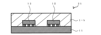
- the first separator 1-a and the second separator 1-c are separated from 1 and then the electronic device 12 mounted on the substrate 11 is covered with the resin sheet 1-b. Thereby, the electronic device package 21 in which the electronic device 12 is covered with the resin sheet 1-b is obtained.
- the substrate 11 is not particularly limited, and examples thereof include a printed wiring board, a ceramic substrate, a silicon substrate, and a metal substrate.
- the resin sheet 1-b of the electronic device package 21 is thermally cured as necessary. Further, if necessary, the resin sheet 1-b of the electronic device package 21 is ground to expose the electronic device 12. In addition, when the electronic device 12 is a SAW filter, grinding is not normally performed. Further, dicing of the electronic device package 21 is performed as necessary (see FIG. 3). Thereby, the chip-shaped electronic device package 31 can be obtained. This process is generally called a chip-on-wafer (COW) process.
- COW chip-on-wafer
- the operator selects an optional resin sheet with a separator (for example, resin sheet 2 with a separator) from the resin sheet group with a separator 101, and then seals the electronic device 12 with the resin sheet with the separator (see FIG. 4).
- a separator for example, resin sheet 2 with a separator
- the adhesive sheet 41 usually has a support 42 and an adhesive layer 43 laminated on the support 42 (see FIG. 4).
- the pressure-sensitive adhesive layer 43 is not particularly limited, but a heat-peelable pressure-sensitive adhesive layer, a radiation curable pressure-sensitive adhesive layer, or the like is usually used because it can be easily peeled off.
- the material for the support 42 is not particularly limited. For example, metal materials such as SUS, plastic materials such as polyimide, polyamideimide, polyetheretherketone, and polyethersulfone.
- an electronic device package can be obtained by performing the following steps. The following steps are suitable for manufacturing a fan-out type wafer level package (WLP).
- WLP fan-out type wafer level package
- the sealing body 51 is thermally cured (the resin sheet 2-b of the sealing body 51 is thermally cured).
- the adhesive sheet 41 is peeled from the sealing body 51 (see FIG. 5).
- the peeling method is not particularly limited, it is preferable to peel the adhesive layer 43 after reducing the adhesive strength.
- the pressure-sensitive adhesive layer 43 is a heat-peelable pressure-sensitive adhesive layer, the pressure-sensitive adhesive layer 43 is heated and peeled after the pressure-sensitive adhesive force of the pressure-sensitive adhesive layer 43 is reduced.
- the sealing body 51 is ground to expose the electronic device 12 (see FIG. 6).
- the grinding method include a grinding method.
- the rewiring 52 is formed in the sealing body 51 using a semi-additive method or the like (see FIG. 7).
- an insulating layer such as polyimide or polybenzoxazole (PBO) is formed on the surface of the sealing body 51 where the rewiring 52 is formed.
- the insulating layer can be formed, for example, by laminating a film such as a dry film resist.
- a bumping process for forming bumps 53 on the rewiring 52 is performed.
- the bumping process can be performed by a known method such as solder ball or solder plating.
- the material of the bump 53 is not particularly limited.
- a tin-lead metal material, a tin-silver metal material, a tin-silver-copper metal material, a tin-zinc metal material, a tin-zinc-bismuth metal material Such as solders (alloys), gold-based metal materials, copper-based metal materials, and the like.
- Dicing of a laminate composed of elements such as the electronic device 12, the resin sheet 2-b, and the rewiring 52 may be performed (see FIG. 8). As described above, it is possible to obtain the electronic device package 61 in which the wiring is drawn outside the chip region.
- the second embodiment is the same as the first embodiment except that the resin sheets with separators 1 to n have a first separator having a color corresponding to the type (specifically, application, composition, etc.) of the resin sheet. is there.
- Examples of color coding of the separator-attached resin sheets 1 to n include, for example, the following Table 2.
- Example 1 the color corresponding to the resin sheet for sealing the SAW filter is white, the color corresponding to the resin sheet for sealing the semiconductor chip is yellow, and the color corresponding to the resin sheet for sealing the MEMS The color is red.
- Example 2 the color according to the SAW filter sealing resin sheet is colorless and transparent, the color according to the semiconductor chip sealing resin sheet is yellow, and the color according to the MEMS sealing resin sheet is red. is there.
- the mark is not particularly limited, and examples thereof include numbers, alphabets, and figures.
- the proper use of the marks on the separator-attached resin sheets 1 to n is not particularly limited.
- a number corresponding to the type of resin sheet can be attached to the first separator.
- Example 1 the mark corresponding to the resin sheet thickness of 200 ⁇ m is the numeral “1”, the mark corresponding to the resin sheet thickness of 150 ⁇ m is the numeral “2”, and the mark corresponding to the resin sheet thickness of 100 ⁇ m is The number is “3”.
- the second separator of the resin sheets 1 to n with a separator may be marked, but it is preferable to mark only the first separator. By attaching a mark only to the first separator, the operator can easily distinguish the first separator and the second separator.
- Embodiment 2 of the second aspect of the present invention is that, except that the resin sheets with separators 1 to n constituting the resin sheet group with separator 101 have a first separator with a mark according to the type of the resin sheet. This is the same as Embodiment 2 of the first invention.
- a number corresponding to the type of resin sheet can be given to the first separator.
- Example 1 the mark corresponding to the high filler type resin sheet is “1” and the mark corresponding to the low filler type resin sheet is “2”, depending on the thin resin sheet.
- the mark is the number “3”.
Landscapes
- Structures Or Materials For Encapsulating Or Coating Semiconductor Devices Or Solid State Devices (AREA)
- Encapsulation Of And Coatings For Semiconductor Or Solid State Devices (AREA)
Abstract
所望の樹脂シートを容易に選択できるセパレータ付き電子デバイス封止用樹脂シート群及びセパレータ付き電子デバイス封止用樹脂シートの選択方法を提供する。 電子デバイス封止用樹脂シートの厚み又は品種ごとにセパレータが色分けされたセパレータ付き電子デバイス封止用樹脂シート群に関する。また、電子デバイス封止用樹脂シートの厚み又は品種に応じたマークが付されたセパレータを備えるセパレータ付き電子デバイス封止用樹脂シートを複数含むセパレータ付き電子デバイス封止用樹脂シート群に関する。
Description
本発明は、セパレータ付き電子デバイス封止用樹脂シート群及びセパレータ付き電子デバイス封止用樹脂シートの選択方法に関する。
従来、電子デバイスパッケージの製造方法として、基板などに固定された1又は複数の電子デバイスを封止樹脂で封止するという方法が知られている。このような封止樹脂として、例えば、樹脂シートが知られている(例えば、特許文献1参照)。
電子デバイスパッケージの製造工場では、多くの品種や厚みの樹脂シートが使用されている。しかしながら、樹脂シートは一般的に黒く、品種や厚みが異なっても外観が似ているため、外観をもとに所望の品種や厚みの樹脂シートを選択することが難しい。樹脂シートの選択ミスが生じることもある。
また、通常、樹脂シートの両面にはセパレータが積層されているが、両セパレータの外観は同じであるため、どちらのセパレータを剥がせばよいか容易に識別できないことがある。
本発明は前記課題を解決し、所望の樹脂シートを容易に選択できるセパレータ付き電子デバイス封止用樹脂シート群及びセパレータ付き電子デバイス封止用樹脂シートの選択方法を提供することを目的とする。
第1の本発明は、電子デバイス封止用樹脂シートの厚み又は品種ごとにセパレータが色分けされたセパレータ付き電子デバイス封止用樹脂シート群に関する。すなわち、第1の本発明のセパレータ付き電子デバイス封止用樹脂シート群は、複数のセパレータ付き樹脂シートからなり、各セパレータ付き樹脂シートは、セパレータ及びセパレータ上に配置された電子デバイス封止用樹脂シートを備え、セパレータは、セパレータ上に配置された電子デバイス封止用樹脂シートの厚み又は品種に応じた色を有する。
第1の本発明のセパレータ付き電子デバイス封止用樹脂シート群は、電子デバイス封止用樹脂シートの厚み又は品種ごとにセパレータが色分けされているため、作業者は色に基づいて所望のセパレータ付き電子デバイス封止用樹脂シートを容易に選択できる。よって、選択ミスを減らすことができる。
第1の本発明のセパレータ付き電子デバイス封止用樹脂シート群は、セパレータを色分けしているため、樹脂シートを着色剤で色分けする必要がない。すなわち、樹脂シートに着色剤を配合する必要がなく、樹脂シート中の着色剤が電子デバイスに及ぼす影響を考慮する必要がないので、樹脂シートを設計し易い。
第1の本発明はまた、電子デバイス封止用樹脂シートの厚み又は品種ごとにセパレータが色分けされたセパレータ付き電子デバイス封止用樹脂シート群を準備するステップと、色に基づいてセパレータ付き電子デバイス封止用樹脂シート群からセパレータ付き電子デバイス封止用樹脂シートを選択するステップとを含むセパレータ付き電子デバイス封止用樹脂シートの選択方法に関する。
第2の本発明は、電子デバイス封止用樹脂シートの厚み又は品種に応じたマークが付されたセパレータを備えるセパレータ付き電子デバイス封止用樹脂シートを複数含むセパレータ付き電子デバイス封止用樹脂シート群に関する。すなわち、第2の本発明のセパレータ付き電子デバイス封止用樹脂シート群は、複数のセパレータ付き樹脂シートからなり、各セパレータ付き樹脂シートは、セパレータ及びセパレータ上に配置された電子デバイス封止用樹脂シートを備え、セパレータは、セパレータ上に配置された電子デバイス封止用樹脂シートの厚み又は品種に応じたマークを有する。
第2の本発明のセパレータ付き電子デバイス封止用樹脂シート群は、電子デバイス封止用樹脂シートの厚み又は品種に応じたマークが付されたセパレータを備えるセパレータ付き電子デバイス封止用樹脂シートを複数含むため、作業者はマークに基づいて所望のセパレータ付き電子デバイス封止用樹脂シートを容易に選択できる。よって、選択ミスを減らすことができる。
第2の本発明のセパレータ付き電子デバイス封止用樹脂シート群は、セパレータに厚み又は品種に応じたマークを付しているため、樹脂シートを着色剤で色分けする必要がない。すなわち、樹脂シートに着色剤を配合する必要がなく、樹脂シート中の着色剤が電子デバイスに及ぼす影響を考慮する必要がないので、樹脂シートを設計し易い。
第2の本発明はまた、電子デバイス封止用樹脂シートの厚み又は品種に応じたマークが付されたセパレータを備えるセパレータ付き電子デバイス封止用樹脂シートを複数含むセパレータ付き電子デバイス封止用樹脂シート群を準備するステップと、マークに基づいてセパレータ付き電子デバイス封止用樹脂シート群からセパレータ付き電子デバイス封止用樹脂シートを選択するステップとを含むセパレータ付き電子デバイス封止用樹脂シートの選択方法に関する。
以下に実施形態を掲げ、本発明を詳細に説明するが、本発明はこれらの実施形態のみに限定されるものではない。
[第1の本発明]
(実施形態1)
セパレータ付き樹脂シート群101は、n(nは2以上の整数を表す)個のセパレータ付き樹脂シートからなる。セパレータ付き樹脂シート群101は、セパレータ付き樹脂シート1~nからなる。
(実施形態1)
セパレータ付き樹脂シート群101は、n(nは2以上の整数を表す)個のセパレータ付き樹脂シートからなる。セパレータ付き樹脂シート群101は、セパレータ付き樹脂シート1~nからなる。
図1は、セパレータ付き樹脂シート群101を構成するセパレータ付き樹脂シート1~3の断面模式図である。セパレータ付き樹脂シート1は、第1のセパレータ1-a、第1のセパレータ1-a上に配置された樹脂シート1-b、及び樹脂シート1-b上に配置された第2のセパレータ1-cを備える。すなわち、セパレータ付き樹脂シート1は、第1のセパレータ1-aと樹脂シート1-bと第2のセパレータ1-cをこの順に積層した構造である。セパレータ付き樹脂シート2は、第1のセパレータ2-a、第1のセパレータ2-a上に配置された樹脂シート2-b、及び樹脂シート2-b上に配置された第2のセパレータ2-cを備える。すなわち、セパレータ付き樹脂シート2は、第1のセパレータ2-aと樹脂シート2-bと第2のセパレータ2-cをこの順に積層した構造である。セパレータ付き樹脂シート3~nも、セパレータ付き樹脂シート1と同様に、第1のセパレータと樹脂シートと第2のセパレータをこの順に積層した構造である。なお、セパレータ付き樹脂シート1~nの樹脂シートは通常、黒色である。
セパレータ付き樹脂シート1~nは、樹脂シートの厚みに応じた色を有する第1のセパレータを有する。したがって、例えば、作業者はセパレータ付き樹脂シート1を探す際に、第1のセパレータ1-aの色に着目することにより、セパレータ付き樹脂シート1を容易に選択できる。
なお、セパレータ付き樹脂シート1~nの第2のセパレータの色は特に限定されない。
セパレータ付き樹脂シート1~nの色分けの例として、例えば、下記表1の例がある。

例1及び例3~5では、樹脂シートの厚み200μmに応じた色が白色であり、樹脂シートの厚み150μmに応じた色が黄色であり、樹脂シートの厚み100μmに応じた色が赤色である。
例2では、樹脂シートの厚み200μmに応じた色が無色透明であり、樹脂シートの厚み150μmに応じた色が黄色であり、樹脂シートの厚み100μmに応じた色が赤色である。
なお、例1及び例4~5は、セパレータ付き樹脂シート1~nの第2のセパレータの色が統一されている。よって、作業者は第1のセパレータ及び第2のセパレータを容易に区別できる。
なお、例3は、セパレータ付き樹脂シート1~n各々の第1のセパレータ及び第2のセパレータの色が同じである。
セパレータ付き樹脂シート1~nの第1のセパレータとしては、例えば、プラスチックシートなどのプラスチック系基材;ゴムシートなどのゴム系基材;発泡シートなどの発泡体基材;金属箔、金属板などの金属系基材;布、不織布、フェルト、ネットなどの繊維系基材;紙などの紙系基材;前記基材の積層体等を用いることができる。なかでも、プラスチック系基材を好適に用いることが好ましい。このようなプラスチック材における素材としては、例えば、ポリエチレン(PE)、ポリプロピレン(PP)、エチレン-プロピレン共重合体等のオレフィン系樹脂;エチレン-酢酸ビニル共重合体(EVA)、アイオノマー樹脂、エチレン-(メタ)アクリル酸共重合体、エチレン-(メタ)アクリル酸エステル(ランダム、交互)共重合体等のエチレンをモノマー成分とする共重合体;ポリエチレンテレフタレート(PET)、ポリエチレンナフタレート(PEN)、ポリブチレンテレフタレート(PBT)等のポリエステル;アクリル系樹脂;ポリ塩化ビニル(PVC);ポリウレタン;ポリカーボネート;ポリフェニレンスルフィド(PPS);ポリアミド(ナイロン)、全芳香族ポリアミド(アラミド)等のアミド系樹脂;ポリエーテルエーテルケトン(PEEK);ポリイミド;ポリエーテルイミド;ポリ塩化ビニリデン;ABS(アクリロニトリル-ブタジエン-スチレン共重合体);セルロース系樹脂;シリコーン樹脂;フッ素樹脂などが挙げられる。
セパレータ付き樹脂シート1~nの第1のセパレータは、剥離処理されていることが好ましい。剥離処理に用いられる離型剤としては、フッ素系剥離剤、長鎖アルキルアクリレート系剥離剤、シリコーン系離型剤等を挙げることができる。
セパレータ付き樹脂シート1~nの第2のセパレータとしては、第1のセパレータで説明したものを使用できる。
セパレータ付き樹脂シート1~nの樹脂シートは、通常、エポキシ樹脂、フェノール樹脂、熱可塑性樹脂、フィラー、シランカップリング剤、硬化促進剤、カーボンブラック、難燃剤などを含む。
作業者はセパレータ付き樹脂シート群101から任意のセパレータ付き樹脂シート(例えば、セパレータ付き樹脂シート1)を選択した後、そのセパレータ付き樹脂シートで電子デバイス12を封止する(図2参照)。
電子デバイス12としては、センサー、MEMS(Micro Electro Mechanical Systems)、SAW(Surface Acoustic Wave)フィルタなどの中空構造を有する電子デバイス(中空型電子デバイス);半導体チップ、IC(集積回路)、トランジスタなどの半導体素子;コンデンサ;抵抗などが挙げられる。なお、中空構造とは、電子デバイスと電子デバイスを搭載した基板との間が中空なっている構造をいう。
セパレータ付き樹脂シート1で電子デバイス12を封止する方法としては、例えば、セパレータ付き樹脂シート1から第1のセパレータ1-a又は第2のセパレータ1-cを剥離した後、又はセパレータ付き樹脂シート1から第1のセパレータ1-a及び第2のセパレータ1-cを剥離した後、基板11に搭載された電子デバイス12を樹脂シート1-bで覆う方法が挙げられる。これにより、電子デバイス12が樹脂シート1-bで覆われた電子デバイスパッケージ21が得られる。基板11としては特に限定されず、例えば、プリント配線基板、セラミック基板、シリコン基板、金属基板などが挙げられる。
電子デバイス12を樹脂シート1-bで覆った後、必要に応じて、電子デバイスパッケージ21の樹脂シート1-bを熱硬化する。また、必要に応じて、電子デバイスパッケージ21の樹脂シート1-bを研削して電子デバイス12を露出させる。なお、電子デバイス12がSAWフィルタである場合、通常は研削を行わない。また、必要に応じて、電子デバイスパッケージ21のダイシングを行う(図3参照)。これにより、チップ状の電子デバイスパッケージ31を得ることができる。
なお、このプロセスは一般にチップ・オン・ウェハ(COW)プロセスと呼ばれる。
なお、このプロセスは一般にチップ・オン・ウェハ(COW)プロセスと呼ばれる。
作業者はセパレータ付き樹脂シート群101から任意のセパレータ付き樹脂シート(例えば、セパレータ付き樹脂シート2)を選択した後、そのセパレータ付き樹脂シートで電子デバイス12を封止する(図4参照)。
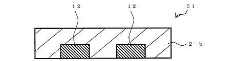
セパレータ付き樹脂シート2で電子デバイス12を封止する方法としては、例えば、セパレータ付き樹脂シート2から第1のセパレータ2-a又は第2のセパレータ2-cを剥離した後、又はセパレータ付き樹脂シート2から第1のセパレータ2-a及び第2のセパレータ2-cを剥離した後、粘着シート41に固定された電子デバイス12を樹脂シート2-bで覆う方法も挙げられる。これにより、電子デバイス12が樹脂シート2-bで覆われた封止体51が得られる。
粘着シート41は、通常、支持体42と、支持体42上に積層された粘着剤層43とを有する(図4参照)。
粘着剤層43としては特に限定されないが、容易に剥離できるという理由から、通常は、熱剥離性粘着剤層、放射線硬化型粘着剤層等を使用する。支持体42の材料としては特に限定されない。例えば、SUS等の金属材料、ポリイミド、ポリアミドイミド、ポリエーテルエーテルケトン、ポリエーテルサルフォン等のプラスチック材料等である。
電子デバイス12を樹脂シート2-bで覆った後に、例えば、以下の工程を行うことで電子デバイスパッケージを得ることができる。以下の工程は、Fan-out(ファンアウト)型ウェハレベルパッケージ(WLP)の製造に好適である。
封止体51を熱硬化する(封止体51の樹脂シート2-bを熱硬化する)。次いで、封止体51から粘着シート41を剥離する(図5参照)。剥離方法は特に限定されないが、粘着剤層43の粘着力を低下させた後に剥離することが好ましい。例えば、粘着剤層43が熱剥離性粘着剤層である場合、粘着剤層43を加熱し、粘着剤層43の粘着力を低下させた後に剥離する。
次いで、必要に応じて封止体51を研削し、電子デバイス12を露出させる(図6参照)。研削方法としては、例えば、グラインディング法などが挙げられる。
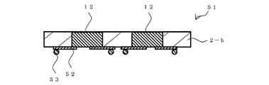
次いで、セミアディティブ法などを利用して、封止体51に再配線52を形成する(図7参照)。
その後、封止体51の再配線52を形成した面に、ポリイミドやポリベンゾオキサゾール(PBO)などの絶縁層を形成する。絶縁層は、例えば、ドライフィルムレジストなどのフィルムをラミネートすることで形成できる。
次いで、再配線52上にバンプ53を形成するバンピング加工を行う。バンピング加工は、半田ボールや半田メッキ等公知の方法で行うことができる。バンプ53の材質は特に限定されないが、例えば、錫-鉛系金属材、錫-銀系金属材、錫-銀-銅系金属材、錫-亜鉛系金属材、錫-亜鉛-ビスマス系金属材等の半田類(合金)や、金系金属材、銅系金属材等である。
電子デバイス12、樹脂シート2-b及び再配線52などの要素からなる積層体のダイシングを行ってもよい(図8参照)。以上により、チップ領域の外側に配線を引き出した電子デバイスパッケージ61得ることができる。
(実施形態2)
セパレータ付き樹脂シート1~nが、樹脂シートの品種(具体的には、用途、組成など)に応じた色を有する第1のセパレータを有する点以外は、実施形態2は実施形態1と同様である。
セパレータ付き樹脂シート1~nが、樹脂シートの品種(具体的には、用途、組成など)に応じた色を有する第1のセパレータを有する点以外は、実施形態2は実施形態1と同様である。
セパレータ付き樹脂シート1~nの色分けの例として、例えば、下記表2の例がある。

例1及び例3~5では、SAWフィルタ封止用樹脂シートに応じた色が白色であり、半導体チップ封止用樹脂シートに応じた色が黄色であり、MEMS封止用樹脂シートに応じた色が赤色である。
例2では、SAWフィルタ封止用樹脂シートに応じた色が無色透明であり、半導体チップ封止用樹脂シートに応じた色が黄色であり、MEMS封止用樹脂シートに応じた色が赤色である。
[第2の本発明]
(実施形態1)
セパレータ付き樹脂シート群101を構成するセパレータ付き樹脂シート1~nが、樹脂シートの厚みに応じたマーク(しるし)が付された第1のセパレータを有する点以外は、第2の本発明の実施形態1は第1の本発明の実施形態1と同様である。
(実施形態1)
セパレータ付き樹脂シート群101を構成するセパレータ付き樹脂シート1~nが、樹脂シートの厚みに応じたマーク(しるし)が付された第1のセパレータを有する点以外は、第2の本発明の実施形態1は第1の本発明の実施形態1と同様である。
マークとしては特に限定されず、例えば、数字、アルファベット、図形などが挙げられる。
セパレータ付き樹脂シート1~nに付すマークの使い分けは特に限定されない。例えば、下記表3のように、樹脂シートの品種に応じた数字を第1のセパレータに付すことができる。
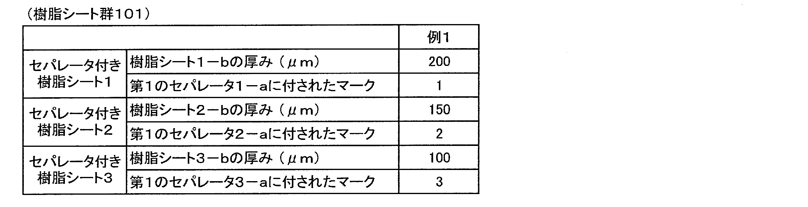
例1では、樹脂シートの厚み200μmに応じたマークが数字の「1」であり、樹脂シートの厚み150μmに応じたマークが数字の「2」であり、樹脂シートの厚み100μmに応じたマークが数字の「3」である。
なお、セパレータ付き樹脂シート1~nの第2のセパレータにもマークを付してもよいが、第1のセパレータにのみマークを付すことが好ましい。第1のセパレータにのみマークを付すことにより、作業者は第1のセパレータ及び第2のセパレータを容易に区別できる。
(実施形態2)
セパレータ付き樹脂シート群101を構成するセパレータ付き樹脂シート1~nが、樹脂シートの品種に応じたマークが付された第1のセパレータを有する点以外は、第2の本発明の実施形態2は第1の本発明の実施形態2と同様である。
セパレータ付き樹脂シート群101を構成するセパレータ付き樹脂シート1~nが、樹脂シートの品種に応じたマークが付された第1のセパレータを有する点以外は、第2の本発明の実施形態2は第1の本発明の実施形態2と同様である。
例えば、下記表4のように、樹脂シートの品種に応じた数字を第1のセパレータに付すことができる。
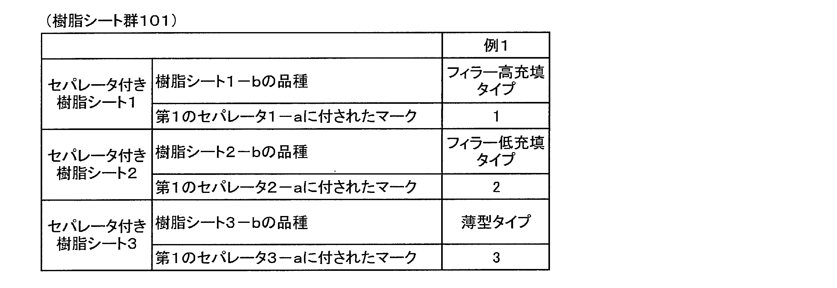
例1では、フィラー高充填タイプの樹脂シートに応じたマークが数字の「1」であり、フィラー低充填タイプの樹脂シートに応じたマークが数字の「2」であり、薄型の樹脂シートに応じたマークが数字の「3」である。
1、2、3 セパレータ付き樹脂シート
1-a、2-a、3-a 第1のセパレータ
1-b、2-b、3-b 樹脂シート
1-c、2-c、3-c 第2のセパレータ
11 基板
12 電子デバイス
21 電子デバイスパッケージ
31 チップ状の電子デバイスパッケージ
41 粘着シート
42 支持体
43 粘着剤層
51 封止体
52 再配線
53 バンプ
61 チップ状の電子デバイスパッケージ
101 セパレータ付き樹脂シート群
1-a、2-a、3-a 第1のセパレータ
1-b、2-b、3-b 樹脂シート
1-c、2-c、3-c 第2のセパレータ
11 基板
12 電子デバイス
21 電子デバイスパッケージ
31 チップ状の電子デバイスパッケージ
41 粘着シート
42 支持体
43 粘着剤層
51 封止体
52 再配線
53 バンプ
61 チップ状の電子デバイスパッケージ
101 セパレータ付き樹脂シート群
Claims (4)
- 電子デバイス封止用樹脂シートの厚み又は品種ごとにセパレータが色分けされたセパレータ付き電子デバイス封止用樹脂シート群。
- 電子デバイス封止用樹脂シートの厚み又は品種ごとにセパレータが色分けされたセパレータ付き電子デバイス封止用樹脂シート群を準備するステップと、
色に基づいてセパレータ付き電子デバイス封止用樹脂シート群からセパレータ付き電子デバイス封止用樹脂シートを選択するステップとを含むセパレータ付き電子デバイス封止用樹脂シートの選択方法。 - 電子デバイス封止用樹脂シートの厚み又は品種に応じたマークが付されたセパレータを備えるセパレータ付き電子デバイス封止用樹脂シートを複数含むセパレータ付き電子デバイス封止用樹脂シート群。
- 電子デバイス封止用樹脂シートの厚み又は品種に応じたマークが付されたセパレータを備えるセパレータ付き電子デバイス封止用樹脂シートを複数含むセパレータ付き電子デバイス封止用樹脂シート群を準備するステップと、
マークに基づいてセパレータ付き電子デバイス封止用樹脂シート群からセパレータ付き電子デバイス封止用樹脂シートを選択するステップとを含むセパレータ付き電子デバイス封止用樹脂シートの選択方法。
Priority Applications (2)
| Application Number | Priority Date | Filing Date | Title |
|---|---|---|---|
| CN201480044656.1A CN105453254A (zh) | 2013-08-09 | 2014-07-03 | 带有隔膜的电子器件密封用树脂片组及带有隔膜的电子器件密封用树脂片的选择方法 |
| SG11201600871WA SG11201600871WA (en) | 2013-08-09 | 2014-07-03 | Separator-attached resin sheet group for sealing electronic device, and method for selecting separator-attached resin sheet for sealing electronic device |
Applications Claiming Priority (2)
| Application Number | Priority Date | Filing Date | Title |
|---|---|---|---|
| JP2013166126A JP2015035523A (ja) | 2013-08-09 | 2013-08-09 | セパレータ付き電子デバイス封止用樹脂シート群及びセパレータ付き電子デバイス封止用樹脂シートの選択方法 |
| JP2013-166126 | 2013-08-09 |
Publications (1)
| Publication Number | Publication Date |
|---|---|
| WO2015019763A1 true WO2015019763A1 (ja) | 2015-02-12 |
Family
ID=52461102
Family Applications (1)
| Application Number | Title | Priority Date | Filing Date |
|---|---|---|---|
| PCT/JP2014/067800 Ceased WO2015019763A1 (ja) | 2013-08-09 | 2014-07-03 | セパレータ付き電子デバイス封止用樹脂シート群及びセパレータ付き電子デバイス封止用樹脂シートの選択方法 |
Country Status (5)
| Country | Link |
|---|---|
| JP (1) | JP2015035523A (ja) |
| CN (1) | CN105453254A (ja) |
| SG (1) | SG11201600871WA (ja) |
| TW (1) | TW201513240A (ja) |
| WO (1) | WO2015019763A1 (ja) |
Families Citing this family (1)
| Publication number | Priority date | Publication date | Assignee | Title |
|---|---|---|---|---|
| CN121443698A (zh) * | 2023-07-31 | 2026-01-30 | 三井化学艾喜缇玛蒂莉亚株式会社 | 粘着性膜、粘着性膜用隔片、粘着性膜的制造方法以及电子装置的制造方法 |
Citations (2)
| Publication number | Priority date | Publication date | Assignee | Title |
|---|---|---|---|---|
| JP2004056141A (ja) * | 2002-07-16 | 2004-02-19 | Nagase & Co Ltd | 半導体装置の樹脂封止方法 |
| JP2010241921A (ja) * | 2009-04-03 | 2010-10-28 | Nitto Denko Corp | 粘着製品 |
Family Cites Families (2)
| Publication number | Priority date | Publication date | Assignee | Title |
|---|---|---|---|---|
| JP5385247B2 (ja) * | 2010-12-03 | 2014-01-08 | 信越化学工業株式会社 | ウエハモールド材及び半導体装置の製造方法 |
| JP2013074184A (ja) * | 2011-09-28 | 2013-04-22 | Nitto Denko Corp | 半導体装置の製造方法 |
-
2013
- 2013-08-09 JP JP2013166126A patent/JP2015035523A/ja active Pending
-
2014
- 2014-07-03 SG SG11201600871WA patent/SG11201600871WA/en unknown
- 2014-07-03 WO PCT/JP2014/067800 patent/WO2015019763A1/ja not_active Ceased
- 2014-07-03 CN CN201480044656.1A patent/CN105453254A/zh active Pending
- 2014-07-28 TW TW103125732A patent/TW201513240A/zh unknown
Patent Citations (2)
| Publication number | Priority date | Publication date | Assignee | Title |
|---|---|---|---|---|
| JP2004056141A (ja) * | 2002-07-16 | 2004-02-19 | Nagase & Co Ltd | 半導体装置の樹脂封止方法 |
| JP2010241921A (ja) * | 2009-04-03 | 2010-10-28 | Nitto Denko Corp | 粘着製品 |
Also Published As
| Publication number | Publication date |
|---|---|
| JP2015035523A (ja) | 2015-02-19 |
| CN105453254A (zh) | 2016-03-30 |
| SG11201600871WA (en) | 2016-03-30 |
| TW201513240A (zh) | 2015-04-01 |
Similar Documents
| Publication | Publication Date | Title |
|---|---|---|
| TWI624369B (zh) | 保護帶、及使用其之半導體裝置之製造方法、以及半導體裝置 | |
| TWI552294B (zh) | A circuit-connecting material, and a method of manufacturing the semiconductor device using the same | |
| JP2017531919A5 (ja) | ||
| KR20090069315A (ko) | 복합형 반도체 장치용 스페이서 시트, 그것을 이용한 반도체 패키지 및 복합형 반도체 장치의 제조 방법, 및 복합형 반도체 장치 | |
| JP5733049B2 (ja) | 接着シート、接着シートの製造方法、接着シートロール、半導体装置の製造方法、及び半導体装置 | |
| JP2014029958A (ja) | 半導体装置の製造方法 | |
| KR20140068761A (ko) | 쉴드 필름, 쉴드 프린트 배선판 및 쉴드 프린트 배선판의 제조 방법 | |
| JPWO2019117258A1 (ja) | 実装構造体の製造方法およびこれに用いられるシート | |
| JP5074738B2 (ja) | 複合型半導体装置用スペーサーシート、及び複合型半導体装置の製造方法 | |
| JP2015079943A (ja) | 前塗布(プレアプライド)アンダーフィル | |
| JP2014019813A (ja) | 熱硬化性樹脂組成物、接着フィルム、ダイシングテープ一体型接着フィルム、半導体装置、多層回路基板および電子部品 | |
| KR20210107709A (ko) | 반도체 장치의 제조 방법, 필름상 접착제 및 다이싱·다이본딩 일체형 필름 | |
| WO2015019763A1 (ja) | セパレータ付き電子デバイス封止用樹脂シート群及びセパレータ付き電子デバイス封止用樹脂シートの選択方法 | |
| CN107636825A (zh) | 半导体用保护膜、半导体装置及复合片 | |
| TWI500077B (zh) | 軟性元件的取出方法及基板之間的分離方法 | |
| TW201338058A (zh) | 半導體裝置的製造方法 | |
| JP5432354B2 (ja) | 配線基板製造用の仮基板及びその製造方法 | |
| JP5728859B2 (ja) | 半導体用フィルムおよび半導体装置の製造方法 | |
| KR20200080799A (ko) | 반도체 패키지용 비전도성 접착필름 및 이를 이용하는 반도체 패키지의 제조방법 | |
| US20160135292A1 (en) | Detachable core substrate and method of manufacturing circuit board using the same | |
| CN104103602B (zh) | 半导体封装件及其制法 | |
| JP2022002231A (ja) | 多層フィルムの製造方法、多層フィルム及び半導体装置の製造方法 | |
| CN104952858A (zh) | 半导体器件、半导体层叠模块构造、层叠模块构造以及它们的制造方法 | |
| JP5720748B2 (ja) | 半導体チップの製造方法 | |
| JP5423563B2 (ja) | 半導体チップの製造方法 |
Legal Events
| Date | Code | Title | Description |
|---|---|---|---|
| WWE | Wipo information: entry into national phase |
Ref document number: 201480044656.1 Country of ref document: CN |
|
| 121 | Ep: the epo has been informed by wipo that ep was designated in this application |
Ref document number: 14834439 Country of ref document: EP Kind code of ref document: A1 |
|
| NENP | Non-entry into the national phase |
Ref country code: DE |
|
| 122 | Ep: pct application non-entry in european phase |
Ref document number: 14834439 Country of ref document: EP Kind code of ref document: A1 |