WO2015019711A1 - 間欠塗布電池電極製造方法 - Google Patents
間欠塗布電池電極製造方法 Download PDFInfo
- Publication number
- WO2015019711A1 WO2015019711A1 PCT/JP2014/065956 JP2014065956W WO2015019711A1 WO 2015019711 A1 WO2015019711 A1 WO 2015019711A1 JP 2014065956 W JP2014065956 W JP 2014065956W WO 2015019711 A1 WO2015019711 A1 WO 2015019711A1
- Authority
- WO
- WIPO (PCT)
- Prior art keywords
- tip
- active material
- current collector
- battery
- layer
- Prior art date
- Legal status (The legal status is an assumption and is not a legal conclusion. Google has not performed a legal analysis and makes no representation as to the accuracy of the status listed.)
- Ceased
Links
Images



Classifications
-
- H—ELECTRICITY
- H01—ELECTRIC ELEMENTS
- H01M—PROCESSES OR MEANS, e.g. BATTERIES, FOR THE DIRECT CONVERSION OF CHEMICAL ENERGY INTO ELECTRICAL ENERGY
- H01M4/00—Electrodes
- H01M4/02—Electrodes composed of, or comprising, active material
- H01M4/04—Processes of manufacture in general
- H01M4/0402—Methods of deposition of the material
- H01M4/0404—Methods of deposition of the material by coating on electrode collectors
-
- H—ELECTRICITY
- H01—ELECTRIC ELEMENTS
- H01M—PROCESSES OR MEANS, e.g. BATTERIES, FOR THE DIRECT CONVERSION OF CHEMICAL ENERGY INTO ELECTRICAL ENERGY
- H01M10/00—Secondary cells; Manufacture thereof
- H01M10/42—Methods or arrangements for servicing or maintenance of secondary cells or secondary half-cells
- H01M10/48—Accumulators combined with arrangements for measuring, testing or indicating the condition of cells, e.g. the level or density of the electrolyte
-
- B—PERFORMING OPERATIONS; TRANSPORTING
- B05—SPRAYING OR ATOMISING IN GENERAL; APPLYING FLUENT MATERIALS TO SURFACES, IN GENERAL
- B05D—PROCESSES FOR APPLYING FLUENT MATERIALS TO SURFACES, IN GENERAL
- B05D1/00—Processes for applying liquids or other fluent materials
- B05D1/26—Processes for applying liquids or other fluent materials performed by applying the liquid or other fluent material from an outlet device in contact with, or almost in contact with, the surface
-
- B—PERFORMING OPERATIONS; TRANSPORTING
- B05—SPRAYING OR ATOMISING IN GENERAL; APPLYING FLUENT MATERIALS TO SURFACES, IN GENERAL
- B05D—PROCESSES FOR APPLYING FLUENT MATERIALS TO SURFACES, IN GENERAL
- B05D2252/00—Sheets
- B05D2252/02—Sheets of indefinite length
-
- B—PERFORMING OPERATIONS; TRANSPORTING
- B05—SPRAYING OR ATOMISING IN GENERAL; APPLYING FLUENT MATERIALS TO SURFACES, IN GENERAL
- B05D—PROCESSES FOR APPLYING FLUENT MATERIALS TO SURFACES, IN GENERAL
- B05D5/00—Processes for applying liquids or other fluent materials to surfaces to obtain special surface effects, finishes or structures
-
- H—ELECTRICITY
- H01—ELECTRIC ELEMENTS
- H01M—PROCESSES OR MEANS, e.g. BATTERIES, FOR THE DIRECT CONVERSION OF CHEMICAL ENERGY INTO ELECTRICAL ENERGY
- H01M4/00—Electrodes
- H01M4/02—Electrodes composed of, or comprising, active material
- H01M4/64—Carriers or collectors
- H01M4/70—Carriers or collectors characterised by shape or form
- H01M4/72—Grids
- H01M4/74—Meshes or woven material; Expanded metal
- H01M4/747—Woven material
-
- Y—GENERAL TAGGING OF NEW TECHNOLOGICAL DEVELOPMENTS; GENERAL TAGGING OF CROSS-SECTIONAL TECHNOLOGIES SPANNING OVER SEVERAL SECTIONS OF THE IPC; TECHNICAL SUBJECTS COVERED BY FORMER USPC CROSS-REFERENCE ART COLLECTIONS [XRACs] AND DIGESTS
- Y02—TECHNOLOGIES OR APPLICATIONS FOR MITIGATION OR ADAPTATION AGAINST CLIMATE CHANGE
- Y02E—REDUCTION OF GREENHOUSE GAS [GHG] EMISSIONS, RELATED TO ENERGY GENERATION, TRANSMISSION OR DISTRIBUTION
- Y02E60/00—Enabling technologies; Technologies with a potential or indirect contribution to GHG emissions mitigation
- Y02E60/10—Energy storage using batteries
Definitions
- the present invention relates to a battery electrode manufacturing method, and more particularly to an intermittent battery electrode manufacturing method in which an active material layer is intermittently applied.
- a positive electrode used for a battery for example, a lithium ion secondary battery, is manufactured by forming a coating layer in which a positive electrode active material is applied with a predetermined film thickness on a current collector made of aluminum foil.
- the negative electrode has applied the negative electrode active material on the collector made from copper foil, and forms the coating layer similarly.
- There are several methods for producing these coating layers For example, there is a method in which an electrode having a predetermined size is prepared by an electrode punching means from an electrode raw material in which an active material is continuously applied on a current collector.
- a desired electrode is produced by an electrode punching means.
- the method of intermittently applying the electrode layer has the advantage that the coating layer that is not used in the final battery electrode in the battery manufacturing process can be reduced, but there is a means for matching the electrode coating layers on the front and back sides. Necessary.
- FIG. 5 is a diagram for explaining an example of a conventional method for producing intermittently applied battery electrodes
- FIG. 5A is a diagram for explaining a coating process
- FIG. 5B is an enlarged cross-sectional view illustrating a portion D of FIG. 5A in which a coating layer is formed on both sides
- FIG. 5C is a plan view for explaining an electrode active material coating layer formed intermittently on the first surface.
- the current collector 101 taken out from the current collector roll 100 moves the shutter of the first surface coating die 102 a corresponding to the length of the intermittent coating layer while moving in the arrow direction at a constant speed.
- the active material is intermittently applied to one surface of the current collector to form the first surface intermittent application layer 103a.
- the second surface coating die control means 105b that has received the detection signal of the tip portion of the first surface intermittent application layer 103a detected by the tip detection means 104 reaches the back surface of the tip portion determined by the moving speed of the current collector.
- the shutter provided on the second surface coating die 102b is opened to start coating, and the shutter is closed after a predetermined time has elapsed, whereby the second surface intermittent coating layer 103b is formed on the opposite surface of the first surface intermittent coating layer 103a. Is forming.
- the first surface intermittent application layer 103a and the second surface intermittent application layer 103b may be misaligned. Further, the amount of positional deviation sometimes differs depending on the position of the electrode.
- the electrode having the displacement of the active material layer on the front and back sides is not provided. It could not be used for a battery, and the produced electrode had to be discarded.
- the present inventors have found that the irregular surface is formed at the front end or the rear end of the intermittent coating layer as described below, resulting in positional displacement.
- the problem of avoiding the formation of the irregular surface 105 that is displaced from the reference surface at the tip of the coating layer is a problem.
- the resolution was difficult.
- the above problem is that even if the irregular surface 105 is small enough not to adversely affect the charge / discharge characteristics of the battery, the leading edge detecting means 104 for detecting the leading edge of the coating portion is not suitable for these irregular surfaces.
- the first surface intermittent coating layer 103a and the second surface intermittent coating layer 103b are identical on the front and back of the current collector. Therefore, misalignment was unavoidable.
- An object of the present invention is to form a tip index indicating a tip of an active material layer to be intermittently applied on a strip-shaped current collector other than a portion where an active material is to be applied, and based on a detection signal of the tip index After forming the intermittent coating layer by applying the active material to the first surface of the current collector, the tip used when forming the active material coating layer of the first surface on the second surface opposite to the first surface.
- an intermittently applied battery electrode manufacturing method that uses the same tip index as the index and starts application of the intermittently applied layer based on the detection signal of the tip index.
- the tip index of the active material layer applied intermittently on the strip-shaped current collector is formed other than the portion where the active material is applied on the current collector surface, and the tip index
- the intermittent coating layer formed on the second surface opposite to the first surface is the same as that used when applying the intermittent coating layer on the first surface. Since it is formed by the tip index, it is possible to provide an intermittently applied battery electrode with excellent quality without causing positional deviation between the front and back sides.
- FIG. 1 is a diagram for explaining one embodiment of a current collector production process in the intermittently applied battery electrode production method of the present invention.
- FIG. 2 is a diagram for explaining another embodiment of the method for producing an intermittently applied battery electrode of the present invention.
- FIG. 3 is a diagram for explaining another embodiment of the method for producing an intermittently applied battery electrode of the present invention.
- FIG. 4 is a diagram for explaining another embodiment of the method for producing an intermittently applied battery electrode of the present invention.
- FIG. 5 is a diagram for explaining an example of a conventional intermittently applied battery electrode manufacturing method.
- FIG. 1 is a diagram for explaining one embodiment of a current collector production process in the intermittently applied battery electrode production method of the present invention.
- a tip index forming means 120 capable of forming a tip index on a metal surface such as a laser engraving machine or an ink jet printing means on a portion of the current collector 101 drawn from the current collector roll 100 that is not scheduled to be coated with an active material.
- the tip index 125 is formed.
- the interval between the adjacent tip indicators 125 is the length of the intermittent application layer in the length direction of the current collector, the length of the portion used as the positive electrode tab and the negative electrode tab, and the length necessary for handling during manufacturing. It can be produced in consideration.
- the battery electrode of the present invention has a center plane parallel to the surface of the current collector, with each tip index 125 having a position in the longitudinal direction of the current collector as a reference position, and an active material coating layer formed on the front and back of the current collector. Is formed at a symmetrical position. Therefore, the positions of the adjacent tip indicators may be arbitrary, but are preferably arranged at an equal pitch in consideration of workability in the assembly process. As described above, the current collector 101 having the tip index 125 formed thereon can be applied to the electrode active material on both surfaces of the current collector in the intermittent application step after being wound around the take-up roll 100b.
- FIG. 2 is a diagram for explaining another embodiment of the current collector manufacturing process in the intermittently applied battery electrode manufacturing method of the present invention.
- FIG. 2A shows a tip position forming unit 120 capable of forming a tip index on a metal surface such as a laser engraving machine or an ink jet coating unit in a region where the active material of the current collector 101 drawn from the current collector roll 100 is not applied.
- the tip index 125 is formed. Between adjacent tip indicators 125, the length of the intermittently applied layer in the length direction of the current collector, the length of the portion used as the positive electrode tab and the negative electrode tab, and the length necessary for handling during manufacturing are taken into consideration. Can be set.
- the tip position forming means In the method described with FIG. 2, first, as shown in FIG. 2A, simultaneously with the formation of the tip index 125 shown in FIG. 2B by the tip position forming means 120 on one surface of the current collector 101, the tip position forming means. Based on the operation signal 120, the active material intermittent application layer 103a is formed from the part corresponding to the tip position by the application die 102a. Thus, the application of the active material on one surface side may be performed by using the operation signal of the tip position forming means as the operation signal of the application die of the intermittent application layer without using the tip position detecting means.
- the tip position detecting means when used, it is necessary to provide the tip position detecting means on the tip position forming means side, but the following advantages can be obtained by using the operation signal of the tip position forming means. it can. That is, as shown in FIG. 2, it is only necessary to provide the tip position detecting means only on one side of the current collector foil, and the number of parts of the coating machine can be reduced.
- the current collector 101 on which the intermittent coating layer is formed is dried by the drying furnace 200 and then wound by the winding roll 100b to obtain a winding roll having an intermittent coating layer of the active material formed on one surface. .
- the winding roll 100b having the active material coating layer formed on one surface is mounted so as to be applied to the surface opposite to the surface on which the active material coating layer is formed.
- the intermittent application layer 103b of the active material is applied by a coating die from the position of the tip index 125 corresponding to the detection signal of the tip position detecting means 104a disposed on the opposite side to the forming means 120 via the current collector foil.
- the winding roll which formed the intermittent application layer of the active material on both surfaces can be obtained by winding the collector which dried in the drying furnace 200, and formed the active material intermittent application layer on both surfaces by the winding roll 100c. it can.
- the battery electrode of the present invention has a center plane parallel to the surface of the current collector, with each tip index 125 having a position in the longitudinal direction of the current collector as a reference position, and an active material coating layer formed on the front and back of the current collector. Is symmetric with respect to. Therefore, the positions of the adjacent tip indicators may be arbitrary, but are preferably arranged at an equal pitch in consideration of workability in the assembly process.
- tip index detection means may be provided on both sides of the coating apparatus. The tip position forming means and the tip position detecting means can be distanced from the coating die so that variations in operation do not occur under the influence of minute changes in the tension applied to the current collector foil or deflection. It is preferable to make it close within the range.
- FIG. 3 is a diagram for explaining another embodiment of the method for producing an intermittently applied battery electrode of the present invention.
- the tip index 125 is formed by the tip index forming means 120.
- the shutter of the first surface coating die 102a is opened to start application of the intermittent electrode layer.
- the shutter of the first surface coating die 102a is closed.
- the application of the active material on the first surface side does not use the tip position detecting means, but the operation signal of the tip position forming means is used as the operation signal of the application die of the intermittent application layer, or the tip index forming means 120.
- Tip position detecting means (not shown) may be provided between the first surface coating die and the first surface coating die, and an operation signal of the tip position forming means may be generated based on the detection signal.
- the active material on the first surface side is formed using the operation signal of the tip position forming means as the operation signal of the application die of the intermittent application layer.
- the intermittent electrode layer 103a is formed on the first surface of the current collector 101 provided with the tip index 125 with the position indicated by the tip index 125 as the tip.
- the current collector on which the first surface intermittent application layer 103a is formed is dried in the drying furnace 200a to complete the first surface intermittent application layer.
- the tip index 125 provided on the first surface reaches the second tip detection means 104b provided in front of the second surface coating die 102b for coating the active material layer on the second surface opposite to the first surface. Then, the second tip index detection unit 104b detects the tip index 125.
- the shutter of the second surface coating die 102b is opened, and the application of the active material layer to the second surface is started.
- the second surface coating die 102b is closed to form the second surface intermittent coating layer 103b as shown in FIG. 3C.
- the current collector on which the second surface intermittent coating layer 103b is formed is completely dried in the drying furnace 200b to complete the coating layer.
- the tip index used for applying the active material layer to the first surface of the current collector can be detected, and the application of the active material to the second surface, which is the opposite surface, can be started.
- the intermittent coating layer can be formed also on the second surface without causing a mutual positional shift on the surface opposite to the first surface, an intermittent coating electrode with excellent positional accuracy can be manufactured.
- the intermittent application operation of the first surface application die and the second surface application die can be performed individually or in conjunction with each other.
- a dancer roll (not shown) is provided before the current collector foil reaches the first surface coating die 102a and the second surface coating die 102b.
- a sudden change in tension is prevented so that the current collector foil is not cut.
- the operation of intermittently applying the active material on the second surface is not performed based on the operation signal of the tip position forming means 120 for the following reason. That is, the distance from the tip position forming means to the second surface coating die is not fixed by the dancer roll.
- the intermittently applied layer 103 applied with the electrode active material from each intermittently applied layer and the electrode tab 132 not applied with the electrode active material are integrated.
- the unit battery electrode 130 can be manufactured by cutting into pieces.
- FIG. 4 is a diagram for explaining another embodiment of the method for producing an intermittently applied battery electrode of the present invention.
- FIG. 4A is a diagram illustrating an intermittent application layer formed on the current collector surface.
- FIG. 4B is an enlarged view for explaining a tip index in the present embodiment.
- the present embodiment is different from the embodiment in that a tip index 129 with identification information in which identification information 127 is integrally formed in addition to the tip index 125 is provided in place of the tip index described with reference to FIGS. ing. Therefore, the tip position is detected by the tip index 125, and each intermittent application layer 103 can be identified.
- the following functions can be obtained by using the identification information 127.
- each position of A, B, C, D, E indicating the position in the width direction of the current collector, an abnormality in thickness, etc.
- the part where the defect is detected can be recorded in association with the identification information 127.
- FIG. 4C is a diagram illustrating the manufactured unit electrode.
- the tip index with identification information is placed on a straight line perpendicular to the length direction of the current collector at each electrode tab formation site. It is arranged to line up.
- each manufactured unit electrode can be managed with the identification information. Therefore, traceability can be improved for a battery manufactured using the unit electrode of this embodiment.
- the tip index with identification information is located inside the battery case after battery assembly, it must be formed on the metal surface by a laser engraving machine so as not to be eluted by battery electrolyte etc. There is. On the other hand, in the thing located outside the battery exterior material, it can form using an inkjet printing means.
- the tip index 129 with identification information described with reference to FIG. 4 may be formed in place of the tip index 125 shown in FIGS.
- identification information does not remain in individual unit electrodes, information on electrodes applied intermittently can be managed collectively as one identification information.
- the displacement of the active material does not necessarily mean that the active material application ends do not completely coincide with each other on the front and back of the current collector, but the electrode is displaced from the intended state. Means. For example, when an electrode is formed in a state where the coated ends of the active material are not intentionally matched on the front and back sides of the current collector, this means a deviation from the state where the electrodes are not intentionally matched.
- the intermittently applied battery electrode manufacturing method of the present invention is a tip index indicator in which an intermittently applied layer formed on each of the first surface of the current collector and the second surface on the opposite side is applied to a portion where the active material layer is not applied. Since the detection is performed by detection, the intermittent coating layer can be formed on the second surface without causing a positional shift with respect to the opposite side of the first surface, and therefore, it is possible to provide a battery electrode without a positional shift of the active material layer. it can. In addition, when identification information is provided in the tip index, the traceability of the battery electrode can be improved.
- DESCRIPTION OF SYMBOLS 100 ... Current collector roll, 100b, 100c ... Winding roll, 101 ... Current collector, 103 ... Intermittent application layer, 120 ... Marking means, 125 ... Tip index, 104a ... First tip detection means, 125 ... tip index, 105a ... first surface coating die control means, 102a ... first surface coating die, 102b ... second surface coating die, 103, 103a, 103b ... intermittent electrode layer, 104a ... first tip index detecting means, 104b ... second tip detecting means, 125 ... tip index, 127 ... identification information, 129 ... identification Advanced indicators with information
Landscapes
- Chemical & Material Sciences (AREA)
- Chemical Kinetics & Catalysis (AREA)
- Electrochemistry (AREA)
- General Chemical & Material Sciences (AREA)
- Engineering & Computer Science (AREA)
- Manufacturing & Machinery (AREA)
- Battery Electrode And Active Subsutance (AREA)
- Secondary Cells (AREA)
Abstract
Description
これらの塗布層の代表的な製造方法には、いくつかの方法がある。例えば、集電体上に連続的に活物質を塗布した電極原反を、電極打ち抜き手段によって所定の大きさの電極を作製する方法である。また、集電体上に間欠的に活物質を塗布した後に電極打ち抜き手段によって所望の電極を作製する方法である。
電極層を間欠的に塗布する方法では、電池製造工程での最終的な電池電極において利用しない塗布層を減少させることができるという利点はあるが、表裏の電極塗布層を一致させるための手段が必要となる。
図5は、従来の間欠塗布電池電極製造方法の一例を説明する図であり、図5Aは、塗布工程を説明する図である。また、図5Bは、両面に塗布層を形成した図5AのDの部分の断面を拡大して説明する断面図である。また、図5Cは、第一面上に間欠的に形成した電極活物質の塗布層を説明する平面図である。
次いで、先端検出手段104が検出した第一面間欠塗布層103aの先端部の検出信号を受信した第二面塗布ダイ制御手段105bは、集電体の移動速度によって決まる前記先端部裏面が到達する時点で第二面塗布ダイ102bに設けたシャッターを開いて塗布を開始し、所定の時間の経過後にシャッターを閉じることで、第一面間欠塗布層103aの反対面に第二面間欠塗布層103bを形成している。
リチウムイオン二次電池では、セパレーターを介して対向する正極活物質層と負極活物質層の位置ずれが電池の特性に大きな影響を及ぼすために、表裏で活物質層の位置ずれを生じた電極を電池に利用することはできず、作製した電極を廃棄せざるを得なかった。
図5Cに示す様に、集電体101の第一面に間欠塗布層103を形成した場合には塗布層の先端には基準面からずれを生じた不規則面105の形成を避けるという問題の解消は困難であった。
上記の問題は、前記の不規則面105が電池の充放電特性に悪影響を及ぼすことがない程度の小さなものであっても、塗布部の先端を検出する先端検出手段104がこれらの不規則面105の一部を先端部107であると誤認して検出することに起因するものであった。
また、第二面塗布ダイの制御手段105bに対しても誤った先端部検出信号を送信する結果、第一面間欠塗布層103aと第二面間欠塗布層103bとが集電体の表裏では一致せずに位置ずれが生じざるを得なかった。
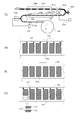
図1は、本発明の間欠塗布電池電極製造方法における集電体の製造工程の一実施態様を説明する図である。
集電体ロール100から引き出した集電体101の活物質の塗布を予定していない部分に、レーザー刻印機またはインクジェット印刷手段等の金属表面に先端指標を形成可能な先端指標形成手段120によって、図1Bに平面図を示すように、先端指標125を形成する。
隣接する先端指標125間の間隔は、集電体の長さ方向の間欠塗布層の長さに、正極タブ、負極タブとして利用する部分の長さ、および製造時の取り扱いに必要な長さを考慮して作製することができる。
以上の様にして、先端指標を125を形成した集電体101は、巻き取りロール100bに巻き取った後に、間欠塗布工程において集電体の両面に電極活物質を塗布することができる。
図2Aは、集電体ロール100から引き出した集電体101の活物質を塗布しない領域に、レーザー刻印機またはインクジェット塗布手段等の金属表面に先端指標を形成可能な先端位置形成手段120によって、図2Bに平面図を示すように、先端指標125を形成する。
隣接する先端指標125間は、集電体の長さ方向の間欠塗布層の長さに、正極タブ、負極タブとして利用する部分の長さ、および製造時の取り扱いに必要な長さを考慮して設定することができる。
このように、一方の面側の活物質の塗布は先端位置検出手段を用いずに、先端位置形成手段の動作信号を、間欠塗布層の塗布ダイの動作信号とすればよい。
また、先端位置検出手段を用いた場合には、先端位置形成手段側にも先端位置検出手段を設ける必要が生じるが、先端位置形成手段の動作信号を用いることで、以下の利点を得ることができる。
すなわち、図2のように先端位置検出手段を集電箔に対して一方の面側だけに設ければよいことになり、塗布機の部品点数を減少することが可能となる。
間欠塗布層を形成した集電体101は、乾燥炉200によって乾燥した後に、巻き取りロール100bによって巻き取って、一方の面に活物質の間欠塗布層を形成した巻き取りロールを得ることができる。
更に乾燥炉200で乾燥して両面に活物質の間欠塗布層を形成した集電体を巻き取りロール100cに巻き取ることで両面に活物質の間欠塗布層を形成した巻き取りロールを得ることができる。
以上の説明では、前記先端位置形成手段120の動作信号に基づいて、先端指標125の形成と同時に、先端位置に対応する部分から塗布ダイ102によって活物質の間欠塗布層103aを形成する例について説明したが、塗布装置の両面に先端指標検出手段を設けても良い。
なお、先端位置形成手段および先端位置検出手段は、集電箔に加わる張力の微小な変化やたわみ等の影響を受けて動作のばらつきが生じることがないように、塗布ダイとの距離を可能な範囲で近づけるのが好ましい。
図3Aに示すように、集電体ロール100から取り出した集電体101を、塗布ダイ方向へと一定の速度で引き出すと、先端指標形成手段120で先端指標125を形成する。 先端指標の形成と同時に、形成した先端指標125の先端位置に対応して第一面塗布ダイ102aのシャッターを開いて間欠電極層の塗布を開始する。次いで、所定の塗布長に達した時点で第一面塗布ダイ102aのシャッターを閉じる。
次いで、第一面間欠塗布層103aを形成した集電体は、乾燥炉200aにおいて乾燥を行って第一面間欠塗布層が完成する。
その結果、集電体101の移動速度から演算した先端位置の到達時点で、第二面塗布ダイ102bのシャッターを開き、第二面へ活物質層の塗布を開始する。
そして、所定の塗布長に達した時点で第二面塗布ダイ102bのシャッターを閉じることで、図3Cに示すように第二面間欠塗布層103bを形成する。
次いで、第二面間欠塗布層103bを形成した集電体は、乾燥炉200bにおいて乾燥を完了して塗布層が完成する。
したがって、第一面の反対面に相互の位置ずれを生じることなく第二面にも間欠塗布層を形成することができるので、位置精度の優れた間欠塗布電極を製造することができる。
また、第二先端位置検出手段104bを、第二面塗布ダイの直前に設けているダンサーロール(図示せず)よりも第二面塗布ダイ102b側に配置することが好ましい。更に、第二先端位置検出手段104bを可能な範囲で第二面塗布ダイに近い位置に形成するのが好ましい。なお、第二面の活物質の間欠塗布の動作を先端位置形成手段120の動作信号に基づいて行わないのは以下の理由による。すなわち、ダンサーロールによって先端位置形成手段から第二面塗布ダイまでの距離が一定にならないためである。
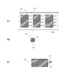
本実施態様は、図1、図2、図3で説明した先端指標に代えて、先端指標125に加えて識別情報127を一体に形成した識別情報付先端指標129を設けている点が相違している。
したがって、先端指標125による先端位置の検出とともに、それぞれの間欠塗布層103の識別を可能としている。
間欠塗布層の作製後の検査において、例えば厚みの異常を検出した場合には、集電体の幅方向の位置を示すA,B,C,D,Eのそれぞれの位置と、厚みの異常等の欠陥を検出した部位等を識別情報127と関連づけて記録することができる。その結果、間欠塗布層から単位電極を切り出した場合に、先の検査において欠陥を検出した単位電極を選別して排除することが可能となる。
図4Cで示す実施態様では、集電体から切り出して作製する各単位電極毎に、それぞれの電極タブの形成部位に、識別情報付先端指標を、集電体の長さ方向に直角な一直線上に並ぶように配置したものである。
このように、集電体から切り出す単位電極のそれぞれの電極タブの形成部に前記識別情報付き先端指標を設けると、作製した各単位電極をそれぞれの識別情報で管理することが可能となる。したがって、本実施態様の単位電極を使用して作製した電池についてはトレーサビリティーを向上することができる。
また、前記識別情報付先端指標が、電池組立後に電池外装材の内部に位置するものにあっては、電池の電解液等によって溶出しないようにするために金属面にレーザー刻印機によって形成する必要がある。一方、電池外装材の外部に位置するものでは、インクジェット印刷手段を用いて形成することができる。
なお、本発明において活物質の位置ずれとは、必ずしも集電体の表裏で活物質の塗布端が完全に一致していないもののみを指すのではなく、意図した状態から電極がずれていることを意味する。例えば、集電体の表裏で活物質の塗布端を意図的に一致させない状態で電極を形成した場合には、その意図的に一致させない状態からのずれのことを意味する。
Claims (5)
- 帯状集電体上に、間欠的に塗布する活物質層の先端を示す先端指標を、活物質を塗布しない部分に形成し、前記先端指標の検出信号に基づき前記集電体の第一面に活物質の塗布を行って間欠塗布層を形成した後に、第一面の反対側の第二面に、前記第一面の活物質塗布層の形成時に用いた先端指標と同一の先端指標を使用して,先端指標の検出信号に基づき、間欠塗布層の塗布を開始することを特徴とする間欠塗布電池電極製造方法。
- 前記先端指標をレーザー捺印機、インクジェット捺印機で刻印することを特徴とする請求項1記載の間欠塗布電池電極製造方法。
- 前記先端指標が識別情報を有していることを特徴とする請求項1または2のいずれかに記載の間欠塗布電池電極製造方法。
- 前記識別情報を塗布層の検査結果情報とリンクさせて、不良品の選別を行うことを特徴とする請求項1から3のいずれか1項記載の間欠塗布電池電極製造方法。
- 請求項1から4のいずれか1項記載の方法によって製造した電池電極を使用した電池を電池使用情報とリンクさせて電池を管理することを特徴とする電池管理方法。
させて電池を管理することを特徴とする電池管理方法。
Priority Applications (2)
| Application Number | Priority Date | Filing Date | Title |
|---|---|---|---|
| US14/904,729 US10236497B2 (en) | 2013-08-06 | 2014-06-17 | Intermittently coated battery electrode manufacturing method |
| JP2015530737A JP6432990B2 (ja) | 2013-08-06 | 2014-06-17 | 間欠塗布電池電極製造方法 |
Applications Claiming Priority (2)
| Application Number | Priority Date | Filing Date | Title |
|---|---|---|---|
| JP2013-163285 | 2013-08-06 | ||
| JP2013163285 | 2013-08-06 |
Publications (1)
| Publication Number | Publication Date |
|---|---|
| WO2015019711A1 true WO2015019711A1 (ja) | 2015-02-12 |
Family
ID=52461053
Family Applications (1)
| Application Number | Title | Priority Date | Filing Date |
|---|---|---|---|
| PCT/JP2014/065956 Ceased WO2015019711A1 (ja) | 2013-08-06 | 2014-06-17 | 間欠塗布電池電極製造方法 |
Country Status (3)
| Country | Link |
|---|---|
| US (1) | US10236497B2 (ja) |
| JP (1) | JP6432990B2 (ja) |
| WO (1) | WO2015019711A1 (ja) |
Cited By (7)
| Publication number | Priority date | Publication date | Assignee | Title |
|---|---|---|---|---|
| WO2018168105A1 (ja) * | 2017-03-17 | 2018-09-20 | 株式会社Screenホールディングス | 塗工装置および塗工方法 |
| JP2023531784A (ja) * | 2020-07-01 | 2023-07-25 | ヴァルタ マイクロバッテリー ゲゼルシャフト ミット ベシュレンクテル ハフツング | 電気化学セルを製造するための方法及びシステム、並びに電気化学セルのための電極 |
| JP2023114987A (ja) * | 2022-02-07 | 2023-08-18 | ハネウェル・インターナショナル・インコーポレーテッド | 基準マーカを有するバッテリ電極の改善されたトレーサビリティ |
| JP2025021492A (ja) * | 2023-08-01 | 2025-02-14 | プライムプラネットエナジー&ソリューションズ株式会社 | 蓄電デバイスの製造方法、記録装置および蓄電デバイス製造装置 |
| WO2025047157A1 (ja) * | 2023-08-30 | 2025-03-06 | パナソニックIpマネジメント株式会社 | 電極板の製造方法、電極板、電極体、および電池 |
| JP2025506800A (ja) * | 2022-08-31 | 2025-03-13 | エルジー エナジー ソリューション リミテッド | 電極基材の切断装置 |
| JP2025516912A (ja) * | 2023-02-02 | 2025-05-30 | エルジー エナジー ソリューション リミテッド | 識別表示認識装置、識別表示認識方法および二次電池の製造方法 |
Families Citing this family (15)
| Publication number | Priority date | Publication date | Assignee | Title |
|---|---|---|---|---|
| JP6794965B2 (ja) * | 2017-09-01 | 2020-12-02 | トヨタ自動車株式会社 | 電極の製造装置および製造方法 |
| CN109546077B (zh) * | 2018-12-26 | 2021-09-21 | 蜂巢能源科技有限公司 | 电极极片及其制作方法、锂离子电池 |
| DE102019133335A1 (de) * | 2019-12-06 | 2021-06-10 | Homag Gmbh | Vorrichtung sowie ein Verfahren zum Beschichten einer Fläche eines Werkstücks |
| KR102808443B1 (ko) * | 2020-05-29 | 2025-05-16 | 주식회사 엘지에너지솔루션 | 이차전지 제조방법 및 이차전지 제조장치 |
| KR102593244B1 (ko) * | 2021-08-13 | 2023-10-25 | 주식회사 엘지에너지솔루션 | 전극 위치 추적시스템 |
| CN116417560B (zh) * | 2022-01-05 | 2025-09-12 | 宁德时代新能源科技股份有限公司 | 电池极片、涂布方法、涂布设备及电池单体 |
| WO2023130338A1 (zh) * | 2022-01-07 | 2023-07-13 | 宁德时代新能源科技股份有限公司 | 极片的叠片方法、装置和叠片机 |
| US20260066356A1 (en) * | 2022-08-29 | 2026-03-05 | Panasonic Energy Co., Ltd. | Electrode plate, electrode body, and battery |
| CN119678258A (zh) * | 2022-08-30 | 2025-03-21 | 松下新能源株式会社 | 电极板和电池 |
| US20240097218A1 (en) | 2022-09-15 | 2024-03-21 | Lg Energy Solution, Ltd. | Systems and methods for generating roll map and manufacturing battery using roll map |
| KR102633848B1 (ko) * | 2022-10-19 | 2024-02-07 | 주식회사 엘지에너지솔루션 | 모니터링 시스템 및 그것의 동작 방법 |
| US20240290936A1 (en) * | 2022-12-15 | 2024-08-29 | W. L. Gore & Associates Gmbh | Intermittent direct deposition process for manufacturing a component of a membrane electrode assembly |
| KR20250016999A (ko) * | 2023-07-26 | 2025-02-04 | 에스케이온 주식회사 | 전극 이상을 검사하는 방법 및 그 장치 |
| KR102940147B1 (ko) * | 2023-08-07 | 2026-03-17 | 주식회사 엘지에너지솔루션 | 이차 전지를 제조하는 방법 |
| KR20260039456A (ko) * | 2024-09-13 | 2026-03-20 | 삼성에스디아이 주식회사 | 코팅 장치 및 방법 |
Citations (9)
| Publication number | Priority date | Publication date | Assignee | Title |
|---|---|---|---|---|
| JPH0919654A (ja) * | 1995-07-06 | 1997-01-21 | Toray Eng Co Ltd | 塗布装置 |
| JPH1110061A (ja) * | 1997-06-26 | 1999-01-19 | Sony Corp | 塗布方法 |
| JP2000208134A (ja) * | 1998-11-12 | 2000-07-28 | Dainippon Printing Co Ltd | 非水電解液二次電池用電極板及びその製造方法 |
| JP2004303549A (ja) * | 2003-03-31 | 2004-10-28 | Toray Ind Inc | プラズマディスプレイ用基板の製造方法および製造装置 |
| JP2007258078A (ja) * | 2006-03-24 | 2007-10-04 | Matsushita Electric Ind Co Ltd | 電極板の塗工幅制御システム及び制御方法 |
| JP2009266739A (ja) * | 2008-04-28 | 2009-11-12 | Hitachi Vehicle Energy Ltd | 二次電池、二次電池の製造方法、及び製造システム |
| JP2011100360A (ja) * | 2009-11-06 | 2011-05-19 | Nissha Printing Co Ltd | タッチ入力シートとその製造方法 |
| JP2011206641A (ja) * | 2010-03-29 | 2011-10-20 | Toppan Printing Co Ltd | 両面間欠塗布装置 |
| JP2013043105A (ja) * | 2011-08-22 | 2013-03-04 | Shibaura Mechatronics Corp | 塗布装置及び塗布方法 |
Family Cites Families (6)
| Publication number | Priority date | Publication date | Assignee | Title |
|---|---|---|---|---|
| US5766356A (en) | 1995-07-06 | 1998-06-16 | Toray Engineering Co., Ltd. | Coating apparatus |
| EP0825659B1 (en) * | 1996-08-22 | 2007-07-18 | Dai Nippon Printing Co., Ltd. | Electrode plate for secondary battery with nonaqueous electrolyte and process for producing the same |
| US6423446B1 (en) | 1998-11-12 | 2002-07-23 | Dai Nippon Printing Co., Ltd. | Electrode plate for secondary battery with nonaqueous electrolyte and process for producing same |
| JP4336869B2 (ja) * | 2001-11-27 | 2009-09-30 | 日本電気株式会社 | 真空成膜装置、真空成膜方法および電池用電極の製造方法 |
| KR100601562B1 (ko) * | 2004-07-29 | 2006-07-19 | 삼성에스디아이 주식회사 | 전극 조립체 및 이를 이용한 리튬 이차 전지 |
| JP2011204612A (ja) * | 2010-03-26 | 2011-10-13 | Mitsubishi Heavy Ind Ltd | 電極板製造装置 |
-
2014
- 2014-06-17 US US14/904,729 patent/US10236497B2/en active Active
- 2014-06-17 JP JP2015530737A patent/JP6432990B2/ja active Active
- 2014-06-17 WO PCT/JP2014/065956 patent/WO2015019711A1/ja not_active Ceased
Patent Citations (9)
| Publication number | Priority date | Publication date | Assignee | Title |
|---|---|---|---|---|
| JPH0919654A (ja) * | 1995-07-06 | 1997-01-21 | Toray Eng Co Ltd | 塗布装置 |
| JPH1110061A (ja) * | 1997-06-26 | 1999-01-19 | Sony Corp | 塗布方法 |
| JP2000208134A (ja) * | 1998-11-12 | 2000-07-28 | Dainippon Printing Co Ltd | 非水電解液二次電池用電極板及びその製造方法 |
| JP2004303549A (ja) * | 2003-03-31 | 2004-10-28 | Toray Ind Inc | プラズマディスプレイ用基板の製造方法および製造装置 |
| JP2007258078A (ja) * | 2006-03-24 | 2007-10-04 | Matsushita Electric Ind Co Ltd | 電極板の塗工幅制御システム及び制御方法 |
| JP2009266739A (ja) * | 2008-04-28 | 2009-11-12 | Hitachi Vehicle Energy Ltd | 二次電池、二次電池の製造方法、及び製造システム |
| JP2011100360A (ja) * | 2009-11-06 | 2011-05-19 | Nissha Printing Co Ltd | タッチ入力シートとその製造方法 |
| JP2011206641A (ja) * | 2010-03-29 | 2011-10-20 | Toppan Printing Co Ltd | 両面間欠塗布装置 |
| JP2013043105A (ja) * | 2011-08-22 | 2013-03-04 | Shibaura Mechatronics Corp | 塗布装置及び塗布方法 |
Cited By (11)
| Publication number | Priority date | Publication date | Assignee | Title |
|---|---|---|---|---|
| WO2018168105A1 (ja) * | 2017-03-17 | 2018-09-20 | 株式会社Screenホールディングス | 塗工装置および塗工方法 |
| JP2018153746A (ja) * | 2017-03-17 | 2018-10-04 | 株式会社Screenホールディングス | 塗工装置および塗工方法 |
| CN110382123A (zh) * | 2017-03-17 | 2019-10-25 | 株式会社斯库林集团 | 涂敷装置以及涂敷方法 |
| CN110382123B (zh) * | 2017-03-17 | 2021-09-10 | 株式会社斯库林集团 | 涂敷装置以及涂敷方法 |
| JP2023531784A (ja) * | 2020-07-01 | 2023-07-25 | ヴァルタ マイクロバッテリー ゲゼルシャフト ミット ベシュレンクテル ハフツング | 電気化学セルを製造するための方法及びシステム、並びに電気化学セルのための電極 |
| JP2023114987A (ja) * | 2022-02-07 | 2023-08-18 | ハネウェル・インターナショナル・インコーポレーテッド | 基準マーカを有するバッテリ電極の改善されたトレーサビリティ |
| JP7684998B2 (ja) | 2022-02-07 | 2025-05-28 | ハネウェル・インターナショナル・インコーポレーテッド | 基準マーカを有するバッテリ電極の改善されたトレーサビリティ |
| JP2025506800A (ja) * | 2022-08-31 | 2025-03-13 | エルジー エナジー ソリューション リミテッド | 電極基材の切断装置 |
| JP2025516912A (ja) * | 2023-02-02 | 2025-05-30 | エルジー エナジー ソリューション リミテッド | 識別表示認識装置、識別表示認識方法および二次電池の製造方法 |
| JP2025021492A (ja) * | 2023-08-01 | 2025-02-14 | プライムプラネットエナジー&ソリューションズ株式会社 | 蓄電デバイスの製造方法、記録装置および蓄電デバイス製造装置 |
| WO2025047157A1 (ja) * | 2023-08-30 | 2025-03-06 | パナソニックIpマネジメント株式会社 | 電極板の製造方法、電極板、電極体、および電池 |
Also Published As
| Publication number | Publication date |
|---|---|
| US10236497B2 (en) | 2019-03-19 |
| US20160164069A1 (en) | 2016-06-09 |
| JP6432990B2 (ja) | 2018-12-05 |
| JPWO2015019711A1 (ja) | 2017-03-02 |
Similar Documents
| Publication | Publication Date | Title |
|---|---|---|
| JP6432990B2 (ja) | 間欠塗布電池電極製造方法 | |
| KR101749435B1 (ko) | 금속판, 금속판의 제조 방법, 및 금속판을 사용해서 증착 마스크를 제조하는 방법 | |
| US20150030935A1 (en) | Battery electrode substrate sheet | |
| JP5383471B2 (ja) | 電極製造システム | |
| US10177358B2 (en) | Film production method and film production device | |
| JP5790576B2 (ja) | 蓄電装置用電極体の製造方法 | |
| JPWO2019193869A1 (ja) | 電極板、電極体及び電池 | |
| CN110186936A (zh) | 膜的制造方法和膜卷绕装置 | |
| CN102555436B (zh) | 烟标烫金系统和烟标烫金工艺 | |
| JP6252766B2 (ja) | 電極の製造方法 | |
| TW201611387A (zh) | 電池隔板用微多孔膜捲繞物及其製造方法 | |
| JP6638562B2 (ja) | マーキング装置 | |
| JP2015076229A (ja) | 電極の製造方法 | |
| JP2014026816A (ja) | 電極の製造方法及び蓄電装置並びに二次電池 | |
| WO2025199998A1 (zh) | 锂电池打标追溯方法 | |
| JP2013074000A (ja) | 積層フィルムコンデンサの製造方法 | |
| JP5672170B2 (ja) | 被プレス物の密度変化評価方法及び積層セラミック電子部品の製造方法 | |
| JP2019093496A (ja) | ロール状ワークの加工情報収集方法 | |
| JP2018139195A (ja) | 電極材料の検査方法、及び電極材料の検査装置 | |
| WO2026033315A1 (en) | Production apparatus of an internal assembly for an electrochemical cell |
Legal Events
| Date | Code | Title | Description |
|---|---|---|---|
| 121 | Ep: the epo has been informed by wipo that ep was designated in this application |
Ref document number: 14834650 Country of ref document: EP Kind code of ref document: A1 |
|
| ENP | Entry into the national phase |
Ref document number: 2015530737 Country of ref document: JP Kind code of ref document: A |
|
| WWE | Wipo information: entry into national phase |
Ref document number: 14904729 Country of ref document: US |
|
| NENP | Non-entry into the national phase |
Ref country code: DE |
|
| 122 | Ep: pct application non-entry in european phase |
Ref document number: 14834650 Country of ref document: EP Kind code of ref document: A1 |