WO2015015830A1 - 半田付け装置、及び、半田付け方法 - Google Patents
半田付け装置、及び、半田付け方法 Download PDFInfo
- Publication number
- WO2015015830A1 WO2015015830A1 PCT/JP2014/057909 JP2014057909W WO2015015830A1 WO 2015015830 A1 WO2015015830 A1 WO 2015015830A1 JP 2014057909 W JP2014057909 W JP 2014057909W WO 2015015830 A1 WO2015015830 A1 WO 2015015830A1
- Authority
- WO
- WIPO (PCT)
- Prior art keywords
- solder
- gas
- flow rate
- storage tank
- soldering
- Prior art date
- Legal status (The legal status is an assumption and is not a legal conclusion. Google has not performed a legal analysis and makes no representation as to the accuracy of the status listed.)
- Ceased
Links
Images








Classifications
-
- B—PERFORMING OPERATIONS; TRANSPORTING
- B23—MACHINE TOOLS; METAL-WORKING NOT OTHERWISE PROVIDED FOR
- B23K—SOLDERING OR UNSOLDERING; WELDING; CLADDING OR PLATING BY SOLDERING OR WELDING; CUTTING BY APPLYING HEAT LOCALLY, e.g. FLAME CUTTING; WORKING BY LASER BEAM
- B23K3/00—Tools, devices or special appurtenances for soldering, e.g. brazing, or unsoldering, not specially adapted for particular methods
- B23K3/06—Solder feeding devices; Solder melting pans
- B23K3/0607—Solder feeding devices
- B23K3/0623—Solder feeding devices for shaped solder piece feeding, e.g. preforms, bumps, balls, pellets, droplets
-
- H—ELECTRICITY
- H05—ELECTRIC TECHNIQUES NOT OTHERWISE PROVIDED FOR
- H05K—PRINTED CIRCUITS; CASINGS OR CONSTRUCTIONAL DETAILS OF ELECTRIC APPARATUS; MANUFACTURE OF ASSEMBLAGES OF ELECTRICAL COMPONENTS
- H05K2203/00—Indexing scheme relating to apparatus or processes for manufacturing printed circuits covered by H05K3/00
- H05K2203/04—Soldering or other types of metallurgic bonding
- H05K2203/044—Solder dip coating, i.e. coating printed conductors, e.g. pads by dipping in molten solder or by wave soldering
-
- H—ELECTRICITY
- H05—ELECTRIC TECHNIQUES NOT OTHERWISE PROVIDED FOR
- H05K—PRINTED CIRCUITS; CASINGS OR CONSTRUCTIONAL DETAILS OF ELECTRIC APPARATUS; MANUFACTURE OF ASSEMBLAGES OF ELECTRICAL COMPONENTS
- H05K3/00—Apparatus or processes for manufacturing printed circuits
- H05K3/30—Assembling printed circuits with electric components, e.g. with resistors
- H05K3/32—Assembling printed circuits with electric components, e.g. with resistors electrically connecting electric components or wires to printed circuits
- H05K3/34—Assembling printed circuits with electric components, e.g. with resistors electrically connecting electric components or wires to printed circuits by soldering
- H05K3/3465—Application of solder
- H05K3/3468—Application of molten solder, e.g. dip soldering
Definitions
- the present invention relates to a technique for jetting molten solder.
- soldering apparatus that performs soldering on an object.
- a soldering apparatus an apparatus in which molten solder is jetted from a jet nozzle, and solder that flows in a state of rising from the nozzle port is brought into contact with the target to solder the target.
- This soldering device is also called a “selective soldering device (or point soldering device)”, and selectively solders only to a partial area of the object, such as an area where electronic components are placed on a printed circuit board. It can be performed.
- a gas supply type soldering apparatus is known (for example, see Patent Document 1).
- solder is jetted from a jet nozzle by supplying gas to a sealed solder reservoir.
- the present invention has been made in view of the above problems, and provides a technique capable of making the flow rate of solder jetted by the jet nozzle constant without directly detecting the flow rate of solder jetted by the jet nozzle. With the goal.
- a first aspect that the present invention can take is a soldering apparatus for performing soldering on an object, a solder storage tank for storing molten solder, and the solder storage tank A jet nozzle for jetting the solder supplied from the gas, a gas supply unit for supplying gas to the solder storage tank and jetting the solder from the jet nozzle, and a flow rate of the gas supplied to the solder storage tank A flow rate detecting unit for detecting the gas, and adjusting the pressure of the gas supplied to the solder storage tank based on the flow rate of the gas detected by the flow rate detection unit, and the gas supplied to the solder storage tank And a pressure adjusting unit that makes the flow rate constant.
- a second aspect that the present invention can take is a soldering method for soldering an object, and (a) a gas is supplied to a solder storage tank that stores molten solder. Supplying and jetting the solder from a jet nozzle; (b) detecting a flow rate of the gas supplied to the solder reservoir; and (c) the gas detected in the step (b). Adjusting the pressure of the gas supplied to the solder storage tank based on the flow rate of the gas to make the flow rate of the gas supplied to the solder storage tank constant.
- the flow rate of the gas supplied to the solder reservoir can be made constant by adjusting the gas pressure based on the flow rate of the gas supplied to the solder reservoir.
- the amount of solder can be made constant without directly detecting the amount of solder jetted by the jet nozzle.
- the soldering apparatus may further include a detection unit that detects an abnormality based on the pressure of the gas adjusted by the pressure adjustment unit.
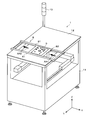
- FIG. 1 is a perspective view showing an external appearance of a soldering apparatus.
- FIG. 2 is an exploded perspective view of the soldering apparatus.
- FIG. 3 is a block diagram showing a schematic configuration of the soldering apparatus.
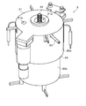
- FIG. 4 is a perspective view showing the appearance of the solder jet device.
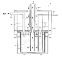
- FIG. 5 is a diagram showing an internal configuration of the solder jet device.
- FIG. 6 is a diagram showing a part of the process of assembling the solder jet device.
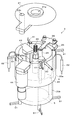
- FIG. 7 is an exploded perspective view of the solder jet device.
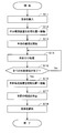
- FIG. 8 is a diagram showing a basic operation flow of the soldering apparatus.
- FIG. 9 is a diagram showing an initial state of the solder jet device.
- FIG. 10 is a view showing one state of the solder jet device.
- FIG. 9 is a diagram showing an initial state of the solder jet device.
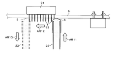
- FIG. 11 is a diagram for explaining the operation of the soldering process.
- FIG. 12 is a view showing one state of the solder jet device.
- FIG. 13 is a view showing a solder jet device as a comparative example.
- FIG. 14 is a view showing one state of the solder jet device.
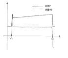
- FIG. 15 is a diagram showing temporal changes in gas pressure and flow rate.
- FIG. 16 is a diagram for explaining the principle that the flow rate of the flowing solder decreases.
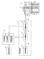
- FIG. 17 is a diagram showing a configuration of a soldering apparatus related to gas supply.
- FIG. 18 is a diagram showing temporal changes in gas pressure and flow rate.
- FIG. 19 is a diagram showing a flow of operation of the soldering apparatus related to gas supply.
- FIG. 1 is a perspective view showing an appearance of a soldering apparatus 1 according to the present embodiment.
- the soldering apparatus 1 has a function of performing soldering (soldering) on the printed circuit board 9 while conveying the printed circuit board 9 as an object.
- the soldering apparatus 1 fixes these electronic components to the printed circuit board 9 by bringing the molten solder into contact with the lower surface of the printed circuit board 9 (the surface on the side where the leads of the electronic components protrude).
- the soldering apparatus 1 is a selective soldering apparatus that can selectively perform soldering on a part of the printed circuit board 9 where electronic components are arranged.
- a region to be soldered on the printed circuit board 9 is referred to as a “target region”.
- the soldering apparatus 1 includes a housing 11, a warning indicator 13, and a board transport mechanism 8.
- the warning indicator 13 is fixed to the side surface of the housing 11 so as to extend in the vertical direction.
- the substrate transport mechanism 8 is provided on an upper surface plate 12 that forms the upper surface of the housing 11.
- XYZ three-dimensional orthogonal coordinate system
- This orthogonal coordinate system is fixed relative to the housing 11.
- the X-axis direction corresponds to the left-right direction
- the Y-axis direction corresponds to the front-rear direction
- the Z-axis direction corresponds to the up-down direction (vertical direction).
- the warning indicator 13 notifies the user such as a worker of information such as a warning by light emission.
- the warning indicator 13 includes a plurality of rotating lamps having different emission colors. These rotating lamps are turned on when a malfunction occurs in the operation of the soldering apparatus 1.
- the substrate transport mechanism 8 transports the printed circuit board 9 placed on the transport pallet 82 in the left-right direction (X-axis direction).
- the substrate transport mechanism 8 includes two conveyors 81 extending along the left-right direction (X-axis direction). These two conveyors 81 move in the directions of arrows AR1 and AR2 in the figure while supporting both ends of the transport pallet 82 in the front-rear direction (Y-axis direction). Thereby, the printed circuit board 9 is conveyed from the right to the left in the figure on the upper surface of the soldering apparatus 1.
- the soldering apparatus 1 performs soldering on the target area of the printed circuit board 9 exposed inside the housing 11 as described above.
- FIG. 2 is an exploded perspective view of the soldering apparatus 1 and mainly shows the internal configuration of the housing 11.
- the soldering apparatus 1 includes a solder jet device 2 that jets molten solder and a triaxial moving mechanism 6 that moves the solder jet device 2 inside a housing 11.
- the solder jet device 2 jets the melted solder and brings the jetted solder into contact with the target region of the printed board 9 to perform soldering on the printed board 9.
- the configuration of the solder jet device 2 will be described in detail later.
- the triaxial moving mechanism 6 includes a fixed portion 60 and three sliders 61, 62, and 63.
- the fixing unit 60 fixes the solder jet device 2.
- the three sliders 61, 62, and 63 extend in the left-right direction (X-axis direction), the front-rear direction (Y-axis direction), and the up-down direction (Z-axis direction), respectively.
- the triaxial moving mechanism 6 can be any of the left-right direction (X-axis direction), the front-rear direction (Y-axis direction), and the up-down direction (Z-axis direction) with the solder jet device 2 fixed by the fixing portion 60
- the solder jet device 2 can be moved. That is, the triaxial moving mechanism 6 can move the solder jet device 2 to an arbitrary position inside the housing 11 while maintaining the posture of the solder jet device 2.
- FIG. 3 is a block diagram showing a schematic configuration of the soldering apparatus 1.
- the soldering apparatus 1 includes an overall control unit 10 and a gas supply unit 7 in addition to the solder jet device 2, the warning indicator 13, the substrate transport mechanism 8, and the triaxial moving mechanism 6 described above.
- the overall control unit 10 is, for example, a programmable logic controller (PLC).
- PLC programmable logic controller
- the overall control unit 10 performs overall processing of the solder jet device 2, the warning indicator 13, the substrate transport mechanism 8, the triaxial moving mechanism 6, and the gas supply unit 7 by performing processing according to a program.
- the gas supply unit 7 supplies a gas that is an inert gas such as nitrogen to the solder jet device 2.
- a gas that is an inert gas such as nitrogen
- FIG. 4 is a perspective view showing the external appearance of the solder jet device 2.
- the vertical direction in the figure corresponds to the vertical direction (the same applies to the subsequent figures).
- the solder jet device 2 includes a solder container 20, a lid 21, and a jet nozzle 22.
- the solder container 20 accommodates the melted solder inside.
- the lid 21 is a circular member that covers the top of the solder container 20.
- the jet nozzle 22 jets solder.
- the lid 21 is provided with two circular openings 21a and 21b. The diameters of the two openings 21a and 21b are different.
- the relatively large diameter central opening 21 a is provided at a position corresponding to the center of the circle in the lid 21.
- the jet nozzle 22 is disposed in the central opening 21a. A part of the jet nozzle 22 protrudes above the lid 21. The upper end of the protruding portion forms a nozzle opening. The jet nozzle 22 jets the melted solder from the nozzle opening.
- the opening portion 21 b having a relatively small diameter is a solder supply port for supplying solder into the solder container 20.
- the opening 21 b is provided at a position away from the central opening 21 a in the lid 21.
- the solder jet device 2 includes a gas introduction pipe 23.
- the gas introduction tube 23 is provided at the upper part of the side surface of the solder container 20 and guides the gas into the solder container 20.
- the gas introduction pipe 23 introduces a gas such as nitrogen supplied from the gas supply unit 7 (see FIG. 3) into the solder container 20.
- FIG. 5 shows the internal configuration of the solder jet device 2.
- FIG. 5 shows a simplified internal configuration of the solder jet device 2 for explanation.
- the solder container 20 of the solder jet device 2 is made of metal such as stainless steel.
- the solder container 20 has a cylindrical shape and has an upper container part 20a and a lower container part 20b having different diameters.
- the upper container portion 20a having a relatively large diameter is disposed above the lower container portion 20b having a relatively small diameter.
- the solder container 20 includes a step portion 20c.
- the step portion 20c extends in the horizontal direction and connects the upper container portion 20a and the lower container portion 20b.
- the solder jet device 2 includes a partition plate 31.
- the partition plate 31 is disposed inside the solder container 20 and extends in the horizontal direction.
- the partition plate 31 is a metal and circular plate material such as stainless steel.
- the partition plate 31 is in contact with the stepped portion 20c of the solder container 20 from above.
- the partition plate 31 is fixed to the step portion 20c with a fastener 39 such as a screw.
- the partition plate 31 partitions the inside of the solder container 20 into an upper part and a lower part, and allows the upper part and the lower part to function as different purpose solder tanks.
- the upper part (inside the upper container part 20 a) than the partition plate 31 inside the solder container 20 functions as the solder collection tank 4.
- the solder recovery tank 4 recovers the solder that has flowed out after being jetted from the jet nozzle 22.
- the lower part (inside the lower container part 20 b) than the partition plate 31 inside the solder container 20 functions as the solder storage tank 5.
- the solder storage tank 5 supplies molten solder to the jet nozzle 22 in response to gas supply.
- the solder recovery tank 4 and the solder storage tank 5 are arranged vertically, so that the overall size of the solder jet device 2 can be made relatively small.
- the partition plate 31 forms the bottom surface of the solder collection tank 4 and the top surface of the solder storage tank 5.
- a communication port 33 is formed in the partition plate 31.
- the communication port 33 communicates the inside of the solder recovery tank 4 with the inside of the solder storage tank 5.
- the communication port 33 is an opening having a circular cross section.
- the solder jet device 2 includes an opening / closing valve 24.
- the on-off valve 24 is disposed above the communication port 33 and opens and closes the communication port 33.
- the on-off valve 24 is a member made of metal such as stainless steel and having a cylindrical shape.
- the on-off valve 24 is disposed so as to extend in the vertical direction.
- the lower end portion of the on-off valve 24 is formed in a hemispherical shape.
- the solder jet device 2 includes an interlocking plate 25.
- the interlocking plate 25 extends in the horizontal direction and is connected to the upper part of the on-off valve 24.
- the on-off valve 24 opens and closes the communication port 33 by moving the interlocking plate 25 up and down.
- the solder recovered in the solder recovery tank 4 returns to the solder storage tank 5.
- a central port 32 is formed at a position corresponding to the center of the circle of the partition plate 31.
- the central port 32 is an opening having a circular cross section.
- the lower end portion of the jet nozzle 22 for jetting the solder is fitted in the central port 32.
- the jet nozzle 22 is made of a metal such as stainless steel and is a cylindrical member having a circular cross section.
- the jet nozzle 22 is disposed so as to pass through the central opening 21a of the lid 21 and extend in the vertical direction.
- the upper end portion 22 a of the jet nozzle 22 is disposed above the lid body 21.
- the solder jet device 2 includes a supply pipe 35.
- the supply pipe 35 is disposed below the central port 32 of the partition plate 31.
- the supply pipe 35 serves as a solder supply path from the solder storage tank 5 to the jet nozzle 22.
- the supply pipe 35 is a cylindrical member made of a metal such as stainless steel and having a circular cross section.
- the supply pipe 35 is disposed so as to extend in the vertical direction.
- the upper end 35a of the supply pipe 35 is joined to the lower surface of the partition plate 31 without a gap by welding or the like.
- An upper end 35 a of the supply pipe 35 surrounds the entire lower part of the central port 32. Thereby, the inside of the supply pipe 35 and the inside of the jet nozzle 22 communicate with each other.
- a lower end 35 b of the supply pipe 35 is disposed in the vicinity of the bottom surface 5 a of the solder storage tank 5 inside the solder storage tank 5.
- the lower end 35 b of the supply pipe 35 faces the bottom surface 5 a of the solder storage tank 5 in a non-contact manner.
- the solder accommodated in the solder storage tank 5 enters the inside of the supply pipe 35 from the lower end 35b of the supply pipe 35.
- the solder that has entered the inside of the supply pipe 35 is supplied to the lower end of the jet nozzle 22 via the central port 32.
- the solder supplied to the jet nozzle 22 rises inside the jet nozzle 22 and jets from the upper end portion 22 a of the jet nozzle 22.
- the solder flowing out of the jet nozzle 22 descends along the outer periphery of the jet nozzle 22, passes through the central opening 21 a, and moves to the solder recovery tank 4.
- the diameter of the jet nozzle 22 is, for example, 14 mm.
- the diameter of the central opening 21a is sufficiently larger than the diameter of the jet nozzle 22 and is, for example, 50 mm. For this reason, a space sufficient for the movement of the solder flowing out from the jet nozzle 22 is formed between the outer periphery of the jet nozzle 22 and the wall surface of the central opening 21a.
- the gas introduction pipe 23 for guiding the gas is disposed so as to pass through the inside of the solder recovery tank 4.
- One end of the gas introduction tube 23 is disposed outside the solder container 20.
- the other end of the gas introduction pipe 23 is connected to a gas introduction port 34 provided in the partition plate 31.
- a gas such as nitrogen supplied from the gas supply unit 7 is supplied to the upper part inside the solder storage tank 5 through the gas introduction pipe 23 and the gas introduction port 34.
- the solder jet device 2 includes a return pipe 36.
- the return pipe 36 is disposed below the communication port 33 of the partition plate 31.
- the return pipe 36 is a return path of solder from the solder recovery tank 4 to the solder storage tank 5.
- the return pipe 36 is made of a metal such as stainless steel and is a cylindrical member having a circular cross section.
- the return pipe 36 is disposed so as to extend in the vertical direction.
- the upper end 36a of the return pipe 36 is joined to the lower surface of the partition plate 31 without a gap by welding or the like.
- An upper end 36 a of the return pipe 36 surrounds the entire lower part of the communication port 33.
- a lower end 36 b of the return pipe 36 is disposed in the vicinity of the bottom surface 5 a of the solder storage tank 5 inside the solder storage tank 5.
- the lower end 36 b of the return pipe 36 faces the bottom surface 5 a of the solder storage tank 5 in a non-contact manner.
- the solder jet device 2 includes a cover member 37.
- the cover member 37 covers the inner surface of the solder container 20 (the inner surface of the lower container portion 20b) from the inside.
- the cover member 37 is made of a metal such as stainless steel, and is a cylindrical member having a circular cross section.
- the diameter of the cover member 37 is larger than the diameters of the supply pipe 35 and the return pipe 36.
- the cover member 37 is disposed along the inner surface of the solder container 20 having a circular cross section (the inner surface of the lower container portion 20b). For this reason, the supply pipe 35 and the return pipe 36 are disposed inside the cover member 37.
- the cover member 37 is preferably in contact with the inner surface of the solder container 20.
- the upper end 37a of the cover member 37 is joined to the lower surface of the partition plate 31 without a gap by welding or the like.
- the upper end 37a of the cover member 37 covers the entire boundary portion between the partition plate 31 and the solder container 20 (the portion where the partition plate 31 and the stepped portion 20c abut) from the inside.
- the lower end 37 b of the cover member 37 is disposed in the vicinity of the bottom surface 5 a of the solder storage tank 5 inside the solder storage tank 5.
- the lower end 37 b of the cover member 37 faces the bottom surface 5 a of the solder storage tank 5 in a non-contact manner.
- the lower ends of the supply pipe 35, the return pipe 36, and the cover member 37 are all disposed in the vicinity of the bottom surface 5a of the solder storage tank 5.
- the heights of the lower ends of the supply pipe 35, the return pipe 36, and the cover member 37 are different.
- the lower end 35b of the supply pipe 35 is arranged highest. That is, the lower end 36 b of the return pipe 36 and the lower end 37 b of the cover member 37 are disposed lower than the lower end 35 b of the supply pipe 35.
- the supply pipe 35, the return pipe 36, and the cover member 37 are joined to the partition plate 31.
- the partition plate 31, the supply pipe 35, the return pipe 36, and the cover member 37 are integrated to form one internal container 30 indicated by hatching in the drawing.
- the solder container 2 is assembled by fitting the inner container 30 into the solder container 20.
- the inner container 30 in which the partition plate 31, the supply pipe 35, the return pipe 36, and the cover member 37 are integrated may be formed by a technique different from welding.
- FIG. 7 is an exploded perspective view showing a detailed configuration of the solder jet device 2.
- FIG. 7 corresponds to a state in which the lid 21 is removed from the solder container 20 shown in FIG.
- the solder jet device 2 includes a valve driving unit 26.
- the valve drive unit 26 is disposed outside the solder container 20.
- the valve drive unit 26 is connected to an interlocking plate 25 connected to the on-off valve 24.
- the interlocking plate 25 has a T-shape when viewed from above.
- the valve drive unit 26 includes a cylinder that is driven to extend and contract, and can move the interlocking plate 25 up and down. Therefore, when the valve drive unit 26 is driven, the on-off valve 24 connected to the interlocking plate 25 moves and opens and closes the communication port 33.
- the solder jet device 2 includes four heaters 41 and four heaters 51.
- the four heaters 41 heat and melt the solder in the solder recovery tank 4.
- the four heaters 51 heat and melt the solder in the solder storage tank 5. These heaters 41 and 51 are respectively installed inside the solder container 20.
- the four heaters 41 for the solder recovery tank 4 are arranged at equal intervals in the circumferential direction of the upper container portion 20a corresponding to the outer wall of the solder recovery tank 4.
- the four heaters 51 for the solder storage tank 5 are arranged at equal intervals in the circumferential direction of the lower container portion 20 b corresponding to the outer wall of the solder storage tank 5. Since the upper container part 20a and the lower container part 20b are cylindrical, by arranging the heaters 41 and 51 in this way, the solder accommodated in each of the upper container part 20a and the lower container part 20b is evenly distributed. Can be heated.
- the upper and lower parts of the solder container 20 can be heated at different timings.
- the soldering device 1 is turned off, the solder accommodated in the solder container 20 of the solder jet device 2 is cooled and solidified.
- the solidified solder is heated from the lower part, the lower solder is melted first.
- the melted lower solder expands and the upper unmelted solder is rapidly pushed up, and a phenomenon of overflowing outside the solder container 20 (solder explosion) may occur.
- the overall control unit 10 energizes the lower heater 51 after a certain period of time has passed since the upper heater 41 is energized. Therefore, after the solder in the upper part of the solder container 20 is sufficiently heated, the solder in the lower part of the solder container 20 is heated. Thereby, since the upper solder is melted first, the above-described phenomenon (solder explosion) can be prevented.
- the solder jet device 2 includes two temperature sensors 42 and 52. These temperature sensors 42 and 52 indirectly detect the temperature of the solder by detecting the temperature of the solder container 20. These temperature sensors 42 and 52 are, for example, thermocouples.
- the temperature sensor 42 detects the temperature of the upper container portion 20 a corresponding to the outer wall of the solder recovery tank 4.
- the temperature sensor 52 detects the temperature of the lower container portion 20 b corresponding to the outer wall of the solder storage tank 5.
- the overall control unit 10 controls the operation of the heaters 41 and 51 based on the detection results of these temperature sensors 42 and 52.
- the solder jet device 2 includes a liquid level detection unit 43.
- the liquid level detection unit 43 detects the level of the solder liquid level in the solder recovery tank 4.
- the liquid level detection unit 43 includes two electrodes 43a having different lengths. One electrode 43a is used to detect a shortage of solder. The other electrode 43a is used to detect solder overflow.
- the liquid level detection unit 43 detects whether the liquid level of the solder is up to the tip position of the electrode 43a through the energized state between the electrode 43a and the solder container 20. When the liquid level detection unit 43 detects the shortage of solder, the solder is supplied into the solder recovery tank 4 through the opening 21b of the lid 21 serving as a solder supply port.
- the solder jet device 2 includes a gas heating unit 44.
- the gas heating unit 44 is disposed outside the solder container 20.
- the gas heating unit 44 is supplied with a gas such as nitrogen from the gas supply unit 7 through a path different from the path to the gas introduction pipe 23.
- the gas heating unit 44 heats the gas supplied from the gas supply unit 7 to, for example, 300 ° C., and supplies the heated gas to the solder recovery tank 4.
- the heated gas supplied from the gas heating unit 44 to the solder recovery tank 4 passes around the jet nozzle 22 in the central opening 21 a and is jetted to the upper part of the solder jet device 2. Therefore, the gas heating unit 44 can preheat the target area of the printed circuit board 9 and can reduce oxidation of the outer periphery of the jet nozzle 22.
- FIG. 8 shows a basic operation flow of the soldering apparatus 1.
- FIG. 8 shows an operation for processing one printed circuit board 9. Therefore, the operation shown in FIG. 8 is repeated every time one printed circuit board 9 is processed. Further, at the start of the operation shown in FIG. 8, the solder jet device 2 stands by at a predetermined initial position and does not jet solder.
- FIG. 9 shows the state of the solder jet device 2 (hereinafter referred to as the initial state) at the start of the operation shown in FIG.
- the initial state of the solder jet device 2 the on-off valve 24 opens the communication port 33.
- the solder S inside the solder recovery tank 4 and the solder S inside the solder storage tank 5 are integrated.
- the liquid level of the solder S is located in the lower part of the solder recovery tank 4. Also, the solder S has entered the jet nozzle 22 up to the same position as the liquid level.
- one printed circuit board 9 that is an object is carried into the soldering apparatus 1 (step S11).
- the substrate transport mechanism 8 receives the printed circuit board 9 on which the flux is applied from an adjacent device or the like, and transports it to a predetermined position (arrow AR1 in FIG. 1).
- the board transport mechanism 8 stops the movement of the printed board 9.
- the triaxial moving mechanism 6 moves the solder jet device 2 from the initial position to a processing position for performing soldering (step S12). Then, during the movement of the solder jet device 2 to the processing position by the triaxial moving mechanism 6, the solder jet device 2 starts jetting the solder S (step S13).
- FIG. 10 shows a state of the solder jet device 2 that starts the jet of the solder S.
- the valve drive unit 26 is driven, and the on-off valve 24 closes the communication port 33.
- the inside of the solder storage tank 5 is in a sealed state.
- the gas supply unit 7 (see FIG. 3) supplies a gas such as pressurized nitrogen to the gas introduction pipe 23 of the solder jet device 2.
- This gas is supplied to the inside of the solder storage tank 5 from the gas introduction port 34 at the upper part of the solder storage tank 5 via the gas introduction pipe 23.
- the pressurized gas is supplied above the liquid level of the solder S accommodated in the solder storage tank 5.
- the solder storage tank 5 receives this gas supply and supplies the solder S to the jet nozzle 22. Since the inside of the solder reservoir 5 is sealed, the solder S accommodated in the solder reservoir 5 is pressed downward by the pressure of the gas. A part of the pressed solder S enters the jet nozzle 22 via the supply pipe 35. The solder S that has entered the jet nozzle 22 rises inside the jet nozzle 22 and jets from the upper end of the jet nozzle 22. As a result, a flow of solder S in a hemispherical shape is formed at the upper end of the jet nozzle 22.
- Solder S flowing out from the jet nozzle 22 descends along the outer peripheral surface of the jet nozzle 22 while covering the entire circumference of the jet nozzle 22.
- the descending solder passes through the central opening 21 a and moves to the solder recovery tank 4.
- the solder S flowing out from the jet nozzle 22 is recovered in the solder recovery tank 4.
- the triaxial moving mechanism 6 moves the solder jet device 2 in the state of jetting the solder S to the processing position.
- a soldering process for selectively soldering the target area of the printed circuit board 9 is performed (step S14).
- FIG. 11 is a diagram for explaining the operation of the soldering process.
- the triaxial moving mechanism 6 raises the solder jet device 2 (arrow AR11).
- the solder S flowing in a state of rising from the upper end portion of the jet nozzle 22 contacts a part of the lead 92 of the electronic component 91 in the target region of the printed circuit board 9.
- the triaxial moving mechanism 6 moves the solder jet device 2 in the horizontal direction within the range of the target area of the printed circuit board 9 (arrow AR12).
- the solder S jetted from the jet nozzle 22 adheres to the entire lead 92 of the electronic component 91 in the target area of the printed circuit board 9.
- the triaxial moving mechanism 6 lowers the solder jet device 2 (arrow AR13).
- the solder jet device 2 can jet the solder S continuously in a predetermined jet period (for example, 60 seconds). The solder jet device 2 completes the soldering process for all the target areas existing on one printed circuit board 9 during this jet period. During the jet period, the position of the liquid surface of the solder S inside the solder reservoir 5 is gradually lowered.
- the triaxial moving mechanism 6 moves the solder jet device 2 from the processing position to the initial position (step S16). Then, during the movement of the solder jet device 2 to the initial position by the triaxial moving mechanism 6, the solder jet device 2 stops the jet of solder (step S17).
- FIG. 12 shows a state of the solder jet device 2 in which the jet of the solder S is stopped.
- the gas supply unit 7 stops supplying gas to the solder jet device 2, and the valve drive unit 26 is driven to open the communication port 33 by the on-off valve 24.
- solder S collected and accumulated in the solder collection tank 4 flows into the solder storage tank 5 via the communication port 33 and the return pipe 36.
- the solder S jetted from the jet nozzle 22 and flowing out without contacting the printed circuit board 9 returns to the solder reservoir 5.
- the gas filled in the solder storage tank 5 is pushed out by such solder S, flows back through the gas introduction pipe 23 via the gas introduction port 34, and is discharged outside the solder jet device 2. Thereafter, when the solder S fills the entire interior of the solder storage tank 5, the solder jet device 2 returns to the initial state shown in FIG.
- step S18 the printed circuit board 9 having been subjected to the soldering process is carried out (step S18).
- the board transport mechanism 8 transports the printed circuit board 9 from a predetermined position to the end of the soldering apparatus 1 and delivers the printed circuit board 9 to an adjacent apparatus or the like (arrow AR2 in FIG. 1).
- the soldering apparatus 1 performs soldering with respect to one printed circuit board 9 by performing a series of operations as described above.
- the solder jet device 2 performs an operation of returning the solder S recovered in the solder recovery tank 4 to the solder storage tank 5 (the operation of FIG. 12). That is, the solder jet device 2 is in a state in which the solder S is not jetted at regular intervals, and the solder S is jetted intermittently. Therefore, it can be said that the soldering apparatus 1 is an intermittent jet soldering apparatus.
- the solder jet device 2 of the present embodiment is configured such that the inside of the solder storage tank 5 is maintained in a sealed state by the return pipe 36 and the cover member 37 joined to the lower surface of the partition plate 31. ing.
- FIG. 13 shows a solder jet device 2a according to a comparative example.
- the configuration of the solder jet device 2a is different from the configuration of the solder jet device 2 according to the present embodiment only in that the return pipe 36 and the cover member 37 are not provided.
- solder jet device 2a in order to jet the solder S from the jet nozzle 22, it is assumed that the communication port 33 is closed by the on-off valve 24 and the gas is supplied to the gas introduction pipe. Also in this case, the gas is supplied from the gas inlet 34 to above the liquid level of the solder S accommodated in the solder reservoir 5, and the extruded solder S is jetted through the supply pipe 35. Jets from the upper end of 22.
- a communication port 33 is formed on the upper surface of the solder storage tank 5. Therefore, when the gas is supplied to the solder storage tank 5 in this way, the gas enters under the communication port 33. Further, the gas also enters the boundary portion between the partition plate 31 and the solder container 20 (the portion where the partition plate 31 and the stepped portion 20c abut). The size of the gas molecules is smaller than the size of the molten solder S molecules.
- the on-off valve 24 closes the communication port 33, the on-off valve 24 and the communication port 33 are in contact with each other.
- a contact portion between the on-off valve 24 and the communication port 33 (a portion surrounded by a broken line A1 in the figure) has a slight gap that allows the gas to enter although the solder S cannot enter. For this reason, the gas supplied to the solder storage tank 5 may leak into the solder recovery tank 4 from such a slight gap.
- solder jet device 2a in the solder jet device 2a according to the comparative example, gas may leak from the solder storage tank 5 to the solder recovery tank 4.
- the gas leaks in this way, the inside of the solder storage tank 5 cannot be maintained in a sealed state. Therefore, the solder S cannot be stably jetted from the jet nozzle 22. As a result, there is a possibility that soldering to the target area of the printed circuit board 9 cannot be performed accurately.
- the upper end 36 a of the return pipe 36 is joined to the lower surface of the partition plate 31 to surround the entire lower part of the communication port 33. It is out. For this reason, when the gas is supplied to the solder storage tank 5, the gas cannot enter the return pipe 36. Therefore, since the inside of the return pipe 36 is filled with the solder S, gas does not enter below the communication port 33. Therefore, it is possible to prevent gas leakage from a contact portion between the on-off valve 24 and the communication port 33 (portion surrounded by a broken line A1 in the drawing). Moreover, since the solder S cannot enter the contact portion between the on-off valve 24 and the communication port 33 due to the size of the molecule, the solder storage tank 5 can be maintained in a sealed state.
- the upper end 37a of the cover member 37 is joined to the lower surface of the partition plate 31, and the entire boundary portion between the partition plate 31 and the solder container 20 (the portion surrounded by the broken line A2 in the figure). Is covered from the inside. Although it is desirable that the cover member 37 and the inner surface of the solder container 20 are in contact with each other, the gap is filled with the solder S even when there is a gap between the cover member 37 and the inner surface of the solder container 20.
- the solder storage tank 5 when the gas is supplied to the solder storage tank 5, the gas cannot enter between the cover member 37 and the inner surface of the solder container 20. Since gas does not enter the boundary portion between the partition plate 31 and the solder container 20, gas leakage from the boundary portion between the partition plate 31 and the solder container 20 can also be prevented. Further, since the solder S cannot enter the boundary portion between the partition plate 31 and the solder container 20 due to the size of the molecule, the solder storage tank 5 can be maintained in a sealed state.
- the inside of the solder storage tank 5 can be maintained in a sealed state by the return pipe 36 and the cover member 37 joined to the lower surface of the partition plate 31. For this reason, the solder S can be stably jetted from the jet nozzle 22. Therefore, the soldering can be accurately performed on the target area of the printed circuit board 9.
- the solder S accommodated in the solder storage tank 5 during the supply of gas to the solder storage tank 5 (during the jet flow) due to a decrease in the amount of solder S in the solder storage tank 5 or the like. It is conceivable that the position of the liquid level is lower than expected. In this case, as shown in FIG. 14, when the position of the liquid surface of the solder S accommodated in the solder storage tank 5 is lowered to the lower end 35b of the supply pipe 35, the gas is supplied to the supply pipe 35 and the jet flow. It goes out of the solder jet device 2 via the nozzle 22.
- the gas does not press the liquid surface of the solder S. Therefore, the solder S does not jet from the jet nozzle 22. For this reason, the position of the liquid level of the solder S accommodated in the solder storage tank 5 is not significantly lower than the lower end 35 b of the supply pipe 35.
- the lower end 36b of the return pipe 36 and the lower end 37b of the cover member 37 are disposed lower than the lower end 35b of the supply pipe 35. According to such a configuration, the position of the liquid level of the solder S accommodated in the solder storage tank 5 is not significantly lower than the lower end 35b of the supply pipe 35. Therefore, the inside of the return pipe 36 and the cover member Gas does not enter between 37 and the inner surface of the solder container 20.
- the flow rate of the solder S jetted by the jet nozzle 22 is proportional to the flow rate of the gas supplied from the gas supply unit 7 to the solder storage tank 5.
- the flow rate Q1 of the solder S jetted by the jet nozzle 22 is expressed by the following equation (1) by the gas flow rate Q2 supplied to the solder storage tank 5 by the gas supply unit 7 and a predetermined coefficient K.
- the coefficient K is a value determined according to the type of gas, the size of the solder jet device, and the like.
- the coefficient K is, for example, 0.7. Since the gas supplied to the solder storage tank 5 is compressed inside the solder storage tank 5, the flow rate Q1 of the solder S jetted is smaller than the flow rate Q2 of this gas.
- the flow rate Q1 of the solder S jetted by the jet nozzle 22 is proportional to the flow rate Q2 of the gas supplied to the solder storage tank 5 by the gas supply unit 7, if the flow rate Q2 of the gas supplied to the solder storage tank 5 can be grasped, the jet flow The flow rate Q1 of the solder S jetted by the nozzle 22 can be indirectly grasped.
- FIG. 15 shows temporal changes in the pressure P and the flow rate Q2 of the gas supplied from the gas supply unit 7 to the solder storage tank 5 in this case.
- the solid line in the figure indicates the gas pressure P.
- the broken line in the figure indicates the gas flow rate Q2.
- the gas supply unit 7 starts supplying gas at time T1 and stops supplying gas at time T2.
- the gas flow rate Q ⁇ b> 2 supplied to the solder storage tank 5 by the gas supply unit 7 is the passage of time. It gradually decreases with time. That is, the flow rate Q1 of the solder S jetted by the jet nozzle 22 gradually decreases with time.
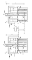
- FIG. 16 is a diagram for explaining this principle.
- the figure on the left shows the state of the solder jet device 2 immediately after the gas supply unit 7 starts supplying gas.
- the diagram on the right side shows the state of the solder jet device 2 after a certain amount of time has elapsed since the gas supply unit 7 started supplying gas.
- the jet nozzle 22 and the supply pipe 35 are regarded as one nozzle and are simply referred to as the jet nozzle 22.
- the solder jet device 2 when the gas supplied into the solder storage tank 5 presses the liquid level of the solder S downward, the jet nozzle 22 starts from the position L of the liquid level of the solder S inside the jet nozzle 22. A force is generated that pushes up the solder S to a position above the upper end 22a. As a result, the solder jet device 2 jets the solder S from the upper end portion 22 a of the jet nozzle 22.
- the position L of the solder S liquid level in the solder reservoir 5 gradually decreases.
- the distance H that needs to push up the solder S inside the jet nozzle 22 gradually increases. Therefore, if a constant pressure is continuously applied to the liquid level of the solder S inside the solder storage tank 5, the force for pushing up the solder S above the upper end portion 22a of the jet nozzle 22 gradually decreases due to the Pascal principle. .
- the flow rate Q1 of the solder S jetted by the jet nozzle 22 (that is, the flow rate Q2 of the gas supplied by the gas supply unit 7) gradually decreases with time.
- the soldering apparatus 1 has a function of making the flow rate Q2 of the gas supplied to the solder storage tank 5 constant.
- FIG. 17 shows a configuration related to gas supply in the soldering apparatus 1.
- the gas supply unit 7 includes a gas supply source 71 and a gas supply path 79.
- the gas supply source 71 is a supply source of a gas such as nitrogen.
- the gas is supplied from the gas supply source 71 to the solder jet device 2 through the gas supply path 79.
- An example of the gas supply source 71 is a cylinder.
- Examples of the gas supply path 79 include a hose.
- the gas supply unit 7 includes a pressure adjustment unit 72 and a flow rate detection unit 73. The pressure adjustment unit 72 and the flow rate detection unit 73 are disposed on the gas supply path 79.
- the pressure adjusting unit 72 adjusts the pressure of the gas flowing through the gas supply path 79 (that is, the gas supplied to the solder reservoir 5).
- the pressure adjustment unit 72 includes a valve inside.
- the pressure adjustment unit 72 adjusts the pressure of the gas flowing through the gas supply path 79 by adjusting the opening degree of the valve in accordance with the electrical signal given from the overall control unit 10.
- the flow rate detection unit 73 detects the flow rate Q2 of the gas flowing through the gas supply path 79 (that is, the gas supplied to the solder reservoir 5).
- the flow rate detection unit 73 is, for example, a thermal mass flow meter, and detects the flow rate Q2 of the gas flowing through the gas supply path 79 by detecting the amount of heat taken away by the gas.
- the flow rate detection unit 73 outputs the detected gas flow rate Q2 to the overall control unit 10 as an electrical signal.
- the overall control unit 10 includes a pressure instruction unit 10a and an abnormality detection unit 10b as part of functions realized by performing processing according to a program.
- the pressure indicator 10a performs feedback control so that the gas flow rate Q2 is constant. That is, based on the gas flow rate Q2 detected by the flow rate detection unit 73, the pressure instruction unit 10a applies the gas pressure to the pressure adjustment unit 72 so that the gas flow rate Q2 approaches a predetermined reference amount. Let them adjust.
- the pressure instruction unit 10a causes the pressure adjustment unit 72 to increase the gas pressure.
- the pressure instruction unit 10a causes the pressure adjustment unit 72 to reduce the gas pressure.
- FIG. 18 shows temporal changes in the pressure P and the flow rate Q2 of the gas supplied to the solder storage tank 5 by the gas supply unit 7 according to the present embodiment.
- the solid line in the figure indicates the gas pressure P.
- the broken line in the figure indicates the gas flow rate Q2.
- the gas supply unit 7 starts supplying gas at time T1 and stops supplying gas at time T2.
- the pressure indicating unit 10a and the pressure adjusting unit 72 adjust the pressure P of the gas supplied to the solder storage tank 5, and gradually increase the pressure P of the gas over time.
- the gas flow rate Q2 supplied to the solder reservoir 5 by the gas supply unit 7 is made constant.
- the flow rate Q1 of the solder S jetted by the jet nozzle 22 is proportional to the gas flow rate Q2. Therefore, the flow rate Q1 of the solder S jetted by the jet nozzle 22 is also constant and stabilized.
- the 17 detects an abnormality of the soldering apparatus 1 based on the gas pressure P adjusted by the pressure instruction unit 10a and the pressure adjustment unit 72.
- the abnormality detection unit 10b shown in FIG. When the soldering apparatus 1 is operating normally, the gas pressure P adjusted by the pressure indicating unit 10a and the pressure adjusting unit 72 is a value within a predetermined reference range.
- the abnormality detection unit 10b determines that an abnormality has occurred when the adjusted gas pressure P is higher than the predetermined first threshold value.
- the abnormality detection unit 10b determines that an abnormality has occurred even when the adjusted gas pressure P is lower than the predetermined second threshold value. Therefore, the abnormality detection unit 10b can easily detect the abnormality of the soldering apparatus 1 based on the gas pressure P adjusted by the pressure instruction unit 10a and the pressure adjustment unit 72.
- FIG. 19 shows a flow of operation of the soldering apparatus 1 relating to gas supply.
- the operation of FIG. 19 is performed in parallel with the operation (steps S13 to S17) from the start of the jet of solder S to the stop of the jet of solder S in FIG.
- step S21 the gas supply unit 7 starts supplying gas to the solder jet device 2 (step S21).
- step S21 the solder jet device 2 starts jetting the solder S.
- step S21 corresponds to step S13 in FIG.
- the flow rate detector 73 detects the flow rate Q2 of the gas supplied to the solder reservoir 5 (step S22).
- the flow rate detection unit 73 outputs the detected gas flow rate Q2 to the overall control unit 10 as an electrical signal.
- the pressure instruction unit 10a of the overall control unit 10 compares the gas flow rate Q2 detected by the flow rate detection unit 73 with a predetermined reference amount (step S23).
- the pressure instruction unit 10a sends a signal to the pressure adjustment unit 72 to increase the gas pressure P (step S25).
- the pressure instruction unit 10a sends a signal to the pressure adjustment unit 72 to lower the gas pressure P (step S26).
- the abnormality detection unit 10b of the overall control unit 10 determines whether or not an abnormality has occurred in the soldering apparatus 1 based on the gas pressure P adjusted by the pressure instruction unit 10a and the pressure adjustment unit 72 ( Step S27). If abnormality detection unit 10b does not detect an abnormality (No in step S28), the process returns to step S22 again, and the same operation as described above is repeated. Such a series of operations is repeated until a predetermined jet period (for example, 60 seconds) ends (during No in step S29).
- a predetermined jet period for example, 60 seconds
- the pressure instruction unit 10a and the pressure adjustment unit 72 adjust the gas pressure P so that the gas flow rate Q2 approaches the reference amount in response to a change in the gas flow rate Q2 supplied to the solder storage tank 5 in real time. To do. As a result, the flow rate Q2 of the gas supplied to the solder reservoir 5 is maintained constant from the start to the end of the jet period. That is, the flow rate Q1 of the solder S jetted by the jet nozzle 22 is maintained constant.
- step S30 the gas supply unit 7 stops supplying gas to the solder jet device 2 (step S30). Thereby, the solder jet device 2 stops the jet of the solder S.
- step S30 corresponds to step S17 in FIG.
- the abnormality detection unit 10b detects an abnormality during the jet period (Yes in step S28), the abnormality detection unit 10b forcibly stops the operation of the soldering apparatus 1 (step S31). Further, the abnormality detection unit 10b turns on the rotating lamp of the warning indicator 13 to notify the user of the abnormality (step S32).
- the flow rate detection unit 73 detects the flow rate Q2 of the gas supplied to the solder storage tank 5, thereby indirectly setting the flow rate Q1 of the solder jetted by the jet nozzle 22. To detect. For this reason, the flow rate Q1 of the solder can be grasped without directly detecting the flow rate Q1 of the flowing solder.
- the pressure indicating unit 10 a and the pressure adjusting unit 72 adjust the pressure of the gas supplied to the solder storage tank 5 based on the gas flow rate Q ⁇ b> 2 detected by the flow rate detection unit 73, and the gas supplied to the solder storage tank 5.
- the flow rate Q2 is kept constant. Therefore, the flow rate Q1 of the solder S jetted by the jet nozzle 22 can be stabilized, and soldering can be accurately performed on the target region of the printed circuit board 9.
- the cross section of the jet nozzle 22, the supply pipe 35 and the return pipe 36 is circular.
- these cross sections may be other shapes such as an ellipse or a rectangle.
- the cross section of the cover member 37 is also circular.
- the cross-sectional shape of the cover member 37 may be a shape that matches the shape of the inner surface of the solder container 20 so that the cover member 37 can be disposed along the inner surface of the solder container 20.
- the partition plate 31 is fixed to the step portion 20c of the solder container 20.
- the partition plate may be fixed to the wall surface of the solder container having no stepped portion. In this case, if the cover member covers the entire boundary portion between the partition plate and the solder container, gas leakage from the boundary portion between the partition plate and the solder container can be prevented.
- the partition plate 31 and the solder container 20 are fixed by the fastener 39.
- the partition plate and the solder container may be joined without a gap by welding or the like.
- a cover member for preventing gas leakage from the boundary portion between the partition plate and the solder container can be omitted.
- the jet nozzle 22 and the supply pipe 35 are configured as separate members.
- the jet nozzle 22 and the supply pipe 35 may be configured as one member.
- the soldering device 1 is configured to move the solder jet device 2 with respect to the printed circuit board 9 disposed at a predetermined position when performing the soldering process.
- the printed circuit board 9 may be configured to move with respect to the solder jet device 2 arranged at a predetermined position.
- the soldering device only needs to include a moving mechanism that changes the relative position between the object and the solder jet device.
- the function described as one block in the above embodiment is not necessarily realized by a single physical element, and may be realized by distributed physical elements.
- the functions described as a plurality of blocks in the above embodiments may be realized by a single physical element.
Landscapes
- Engineering & Computer Science (AREA)
- Mechanical Engineering (AREA)
- Electric Connection Of Electric Components To Printed Circuits (AREA)
- Molten Solder (AREA)
Abstract
Description
図1は、本実施の形態に係る半田付け装置1の外観を示す斜視図である。半田付け装置1は、対象物となるプリント基板9を搬送しながら、該プリント基板9に対して半田(はんだ)付けを行う機能を有している。
次に、半田噴流装置2の構成について説明する。図4は、半田噴流装置2の外観を示す斜視図である。図中の縦方向は、上下方向に相当する(以降の図においても同様)。
図8は、半田付け装置1の基本的な動作の流れを示している。図8は、一つのプリント基板9を処理する動作を示している。したがって、図8に示す動作は、一つのプリント基板9を処理するごとに繰り返される。また、図8に示す動作の開始時点においては、半田噴流装置2は、予め定められた初期位置で待機しており、半田を噴流していない。
次に、半田Sを噴流する状態(図10に示す状態)において、半田貯留槽5の内部を密封状態に維持する手法について説明する。本実施の形態の半田噴流装置2においては、区画板31の下面に接合された戻り管36及びカバー部材37により、このような半田貯留槽5の内部が密封状態に維持されるように構成されている。
次に、半田貯留槽5への気体の供給について説明する。前述のように、気体供給部7が窒素などの加圧した気体を半田噴流装置2の半田貯留槽5に供給することにより、噴流ノズル22から半田Sが噴流される。
本実施の形態に係る半田噴流装置2では、係数Kは例えば0.7である。半田貯留槽5に供給された気体は半田貯留槽5の内部で圧縮されるため、この気体の流量Q2よりも噴流する半田Sの流量Q1は少なくなる。
以上、本発明の実施の形態について説明してきたが、この発明は上記実施の形態に限定されるものではなく様々な変形が可能である。以下では、このような変形例について説明する。上記実施の形態及び以下で説明する形態を含む全ての形態は、適宜に組み合わせ可能である。
Claims (3)
- 対象物に対して半田付けを行う半田付け装置であって、
溶融された半田を収容する半田貯留槽と、
前記半田貯留槽から供給された前記半田を噴流する噴流ノズルと、
前記半田貯留槽に気体を供給して、前記噴流ノズルから前記半田を噴流させる気体供給部と、
前記半田貯留槽に供給される前記気体の流量を検出する流量検出部と、
前記流量検出部に検出された前記気体の流量に基づいて前記半田貯留槽に供給される前記気体の圧力を調整し、前記半田貯留槽に供給される前記気体の流量を一定にする圧力調整部と、
を備えている、半田付け装置。 - 請求項1に記載の半田付け装置において、
前記圧力調整部が調整した前記気体の圧力に基づいて、異常を検出する検出部をさらに備えている、半田付け装置。 - 対象物に対して半田付けを行う半田付け方法であって、
(a)溶融された半田を収容する半田貯留槽に気体を供給して、噴流ノズルから前記半田を噴流させる工程と、
(b)前記半田貯留槽に供給される前記気体の流量を検出する工程と、
(c)前記工程(b)で検出された前記気体の流量に基づいて前記半田貯留槽に供給される前記気体の圧力を調整し、前記半田貯留槽に供給される前記気体の流量を一定にする工程と、
を備えている、半田付け方法。
Priority Applications (1)
| Application Number | Priority Date | Filing Date | Title |
|---|---|---|---|
| CN201480042680.1A CN105408047B (zh) | 2013-07-29 | 2014-03-20 | 钎焊装置以及钎焊方法 |
Applications Claiming Priority (2)
| Application Number | Priority Date | Filing Date | Title |
|---|---|---|---|
| JP2013156812A JP5384766B1 (ja) | 2013-07-29 | 2013-07-29 | 半田付け装置、及び、半田付け方法 |
| JP2013-156812 | 2013-07-29 |
Publications (1)
| Publication Number | Publication Date |
|---|---|
| WO2015015830A1 true WO2015015830A1 (ja) | 2015-02-05 |
Family
ID=50036608
Family Applications (1)
| Application Number | Title | Priority Date | Filing Date |
|---|---|---|---|
| PCT/JP2014/057909 Ceased WO2015015830A1 (ja) | 2013-07-29 | 2014-03-20 | 半田付け装置、及び、半田付け方法 |
Country Status (3)
| Country | Link |
|---|---|
| JP (1) | JP5384766B1 (ja) |
| CN (1) | CN105408047B (ja) |
| WO (1) | WO2015015830A1 (ja) |
Families Citing this family (2)
| Publication number | Priority date | Publication date | Assignee | Title |
|---|---|---|---|---|
| US10610943B2 (en) | 2016-06-29 | 2020-04-07 | Fujitsu Ten Limited | Flux applying method and flux applying apparatus |
| JP6849471B2 (ja) * | 2017-02-15 | 2021-03-24 | 株式会社デンソーテン | 圧送圧力調整装置および圧送圧力調整方法 |
Citations (3)
| Publication number | Priority date | Publication date | Assignee | Title |
|---|---|---|---|---|
| JPH0590467A (ja) * | 1991-09-30 | 1993-04-09 | Hitachi Ltd | はんだコート装置 |
| JP2000071066A (ja) * | 1998-08-28 | 2000-03-07 | Tokyo Seisan Giken Kk | 窒素パッケージ一体型半田槽 |
| US20080067219A1 (en) * | 2004-10-05 | 2008-03-20 | Linde Aktiengesellschaft | Apparatus and Method for Wave Soldering |
Family Cites Families (6)
| Publication number | Priority date | Publication date | Assignee | Title |
|---|---|---|---|---|
| JP2930350B2 (ja) * | 1990-02-06 | 1999-08-03 | 松下電器産業株式会社 | 半田噴流装置 |
| JPH07253440A (ja) * | 1994-03-16 | 1995-10-03 | Osaka Asahi Kagaku Kk | 溶融半田の噴流の流速測定用治具 |
| JP3638415B2 (ja) * | 1997-01-20 | 2005-04-13 | 日本電熱計器株式会社 | ガス雰囲気はんだ付け装置 |
| DE10008031A1 (de) * | 2000-02-15 | 2001-08-16 | Bos Berlin Oberspree Sondermas | Verfahren und Vorrichtung zum Verfüllen von Kavitäten |
| JP3789464B2 (ja) * | 2004-09-21 | 2006-06-21 | 満男 海老澤 | 半田付け装置 |
| CN201676786U (zh) * | 2010-04-28 | 2010-12-22 | 台达电子工业股份有限公司 | 喷雾控制装置 |
-
2013
- 2013-07-29 JP JP2013156812A patent/JP5384766B1/ja active Active
-
2014
- 2014-03-20 CN CN201480042680.1A patent/CN105408047B/zh active Active
- 2014-03-20 WO PCT/JP2014/057909 patent/WO2015015830A1/ja not_active Ceased
Patent Citations (3)
| Publication number | Priority date | Publication date | Assignee | Title |
|---|---|---|---|---|
| JPH0590467A (ja) * | 1991-09-30 | 1993-04-09 | Hitachi Ltd | はんだコート装置 |
| JP2000071066A (ja) * | 1998-08-28 | 2000-03-07 | Tokyo Seisan Giken Kk | 窒素パッケージ一体型半田槽 |
| US20080067219A1 (en) * | 2004-10-05 | 2008-03-20 | Linde Aktiengesellschaft | Apparatus and Method for Wave Soldering |
Also Published As
| Publication number | Publication date |
|---|---|
| JP5384766B1 (ja) | 2014-01-08 |
| JP2015024435A (ja) | 2015-02-05 |
| CN105408047A (zh) | 2016-03-16 |
| CN105408047B (zh) | 2017-11-10 |
Similar Documents
| Publication | Publication Date | Title |
|---|---|---|
| WO2014199694A1 (ja) | 半田付け装置、及び、半田付け方法 | |
| US20220369473A1 (en) | Method for Soldering an Electronic Component to a Circuit Board by Jetting Liquefied Solder into a Through Hole | |
| US12205835B2 (en) | Apparatus having closed loop IR camera heat detection system and method | |
| EP3238858B1 (en) | Low-pressure casting device and low-pressure casting method | |
| JP5433098B1 (ja) | 半田噴流装置、及び、半田付け装置 | |
| JP5384766B1 (ja) | 半田付け装置、及び、半田付け方法 | |
| JP4869729B2 (ja) | 高粘性流体塗布システム | |
| KR20150112809A (ko) | 수지 성형 장치 및 수지 성형 방법 | |
| JP5433107B1 (ja) | 半田噴流装置、及び、半田付け装置 | |
| US7631476B2 (en) | Steam-replacement deaeration apparatus for use in bag packaging | |
| JP5433103B1 (ja) | 半田噴流装置、及び、半田付け装置 | |
| JP4959352B2 (ja) | 半田供給装置および半田供給方法 | |
| EP4255660A1 (en) | Apparatus having closed loop ir camera heat detection system and method | |
| JP5591172B2 (ja) | 半田付け装置及び自動半田付け装置 | |
| CN109202201A (zh) | 焊接装置及焊接方法 | |
| JP6089193B2 (ja) | 半田処理装置 | |
| CN103442463B (zh) | 一种防干烧的厚膜加热装置及即热式加热设备 | |
| JP4399064B2 (ja) | マーキング装置のインク容器 | |
| JP6563885B2 (ja) | 半田ごて温度測定システム及び半田ごて温度測定方法 | |
| JP5591382B2 (ja) | 半田付け装置 | |
| JP6618420B2 (ja) | 温度測定装置および温度測定方法 | |
| KR200392817Y1 (ko) | 인쇄회로기판의 부분 납땜 장치 | |
| JP2003133359A (ja) | 半田バンプ形成方法、及び半田バンプ形成装置 | |
| TWI598279B (zh) | Electronic parts conveying apparatus and electronic parts inspection apparatus | |
| JP2021502240A (ja) | 基材をコーティングするためのシステム及び方法 |
Legal Events
| Date | Code | Title | Description |
|---|---|---|---|
| WWE | Wipo information: entry into national phase |
Ref document number: 201480042680.1 Country of ref document: CN |
|
| 121 | Ep: the epo has been informed by wipo that ep was designated in this application |
Ref document number: 14831841 Country of ref document: EP Kind code of ref document: A1 |
|
| WWE | Wipo information: entry into national phase |
Ref document number: IDP00201600477 Country of ref document: ID |
|
| NENP | Non-entry into the national phase |
Ref country code: DE |
|
| 122 | Ep: pct application non-entry in european phase |
Ref document number: 14831841 Country of ref document: EP Kind code of ref document: A1 |