WO2015012388A1 - 液晶表示装置 - Google Patents
液晶表示装置 Download PDFInfo
- Publication number
- WO2015012388A1 WO2015012388A1 PCT/JP2014/069691 JP2014069691W WO2015012388A1 WO 2015012388 A1 WO2015012388 A1 WO 2015012388A1 JP 2014069691 W JP2014069691 W JP 2014069691W WO 2015012388 A1 WO2015012388 A1 WO 2015012388A1
- Authority
- WO
- WIPO (PCT)
- Prior art keywords
- liquid crystal
- crystal panel
- display device
- crystal display
- housing
- Prior art date
- Legal status (The legal status is an assumption and is not a legal conclusion. Google has not performed a legal analysis and makes no representation as to the accuracy of the status listed.)
- Ceased
Links
Images




Classifications
-
- G—PHYSICS
- G02—OPTICS
- G02F—OPTICAL DEVICES OR ARRANGEMENTS FOR THE CONTROL OF LIGHT BY MODIFICATION OF THE OPTICAL PROPERTIES OF THE MEDIA OF THE ELEMENTS INVOLVED THEREIN; NON-LINEAR OPTICS; FREQUENCY-CHANGING OF LIGHT; OPTICAL LOGIC ELEMENTS; OPTICAL ANALOGUE/DIGITAL CONVERTERS
- G02F1/00—Devices or arrangements for the control of the intensity, colour, phase, polarisation or direction of light arriving from an independent light source, e.g. switching, gating or modulating; Non-linear optics
- G02F1/01—Devices or arrangements for the control of the intensity, colour, phase, polarisation or direction of light arriving from an independent light source, e.g. switching, gating or modulating; Non-linear optics for the control of the intensity, phase, polarisation or colour
- G02F1/13—Devices or arrangements for the control of the intensity, colour, phase, polarisation or direction of light arriving from an independent light source, e.g. switching, gating or modulating; Non-linear optics for the control of the intensity, phase, polarisation or colour based on liquid crystals, e.g. single liquid crystal display cells
- G02F1/133—Constructional arrangements; Operation of liquid crystal cells; Circuit arrangements
- G02F1/1333—Constructional arrangements; Manufacturing methods
- G02F1/133308—Support structures for LCD panels, e.g. frames or bezels
-
- G—PHYSICS
- G02—OPTICS
- G02F—OPTICAL DEVICES OR ARRANGEMENTS FOR THE CONTROL OF LIGHT BY MODIFICATION OF THE OPTICAL PROPERTIES OF THE MEDIA OF THE ELEMENTS INVOLVED THEREIN; NON-LINEAR OPTICS; FREQUENCY-CHANGING OF LIGHT; OPTICAL LOGIC ELEMENTS; OPTICAL ANALOGUE/DIGITAL CONVERTERS
- G02F1/00—Devices or arrangements for the control of the intensity, colour, phase, polarisation or direction of light arriving from an independent light source, e.g. switching, gating or modulating; Non-linear optics
- G02F1/01—Devices or arrangements for the control of the intensity, colour, phase, polarisation or direction of light arriving from an independent light source, e.g. switching, gating or modulating; Non-linear optics for the control of the intensity, phase, polarisation or colour
- G02F1/13—Devices or arrangements for the control of the intensity, colour, phase, polarisation or direction of light arriving from an independent light source, e.g. switching, gating or modulating; Non-linear optics for the control of the intensity, phase, polarisation or colour based on liquid crystals, e.g. single liquid crystal display cells
- G02F1/133—Constructional arrangements; Operation of liquid crystal cells; Circuit arrangements
- G02F1/1333—Constructional arrangements; Manufacturing methods
- G02F1/1339—Gaskets; Spacers; Sealing of cells
-
- G—PHYSICS
- G02—OPTICS
- G02F—OPTICAL DEVICES OR ARRANGEMENTS FOR THE CONTROL OF LIGHT BY MODIFICATION OF THE OPTICAL PROPERTIES OF THE MEDIA OF THE ELEMENTS INVOLVED THEREIN; NON-LINEAR OPTICS; FREQUENCY-CHANGING OF LIGHT; OPTICAL LOGIC ELEMENTS; OPTICAL ANALOGUE/DIGITAL CONVERTERS
- G02F1/00—Devices or arrangements for the control of the intensity, colour, phase, polarisation or direction of light arriving from an independent light source, e.g. switching, gating or modulating; Non-linear optics
- G02F1/01—Devices or arrangements for the control of the intensity, colour, phase, polarisation or direction of light arriving from an independent light source, e.g. switching, gating or modulating; Non-linear optics for the control of the intensity, phase, polarisation or colour
- G02F1/13—Devices or arrangements for the control of the intensity, colour, phase, polarisation or direction of light arriving from an independent light source, e.g. switching, gating or modulating; Non-linear optics for the control of the intensity, phase, polarisation or colour based on liquid crystals, e.g. single liquid crystal display cells
- G02F1/133—Constructional arrangements; Operation of liquid crystal cells; Circuit arrangements
- G02F1/1333—Constructional arrangements; Manufacturing methods
- G02F1/133308—Support structures for LCD panels, e.g. frames or bezels
- G02F1/133325—Assembling processes
-
- G—PHYSICS
- G02—OPTICS
- G02F—OPTICAL DEVICES OR ARRANGEMENTS FOR THE CONTROL OF LIGHT BY MODIFICATION OF THE OPTICAL PROPERTIES OF THE MEDIA OF THE ELEMENTS INVOLVED THEREIN; NON-LINEAR OPTICS; FREQUENCY-CHANGING OF LIGHT; OPTICAL LOGIC ELEMENTS; OPTICAL ANALOGUE/DIGITAL CONVERTERS
- G02F1/00—Devices or arrangements for the control of the intensity, colour, phase, polarisation or direction of light arriving from an independent light source, e.g. switching, gating or modulating; Non-linear optics
- G02F1/01—Devices or arrangements for the control of the intensity, colour, phase, polarisation or direction of light arriving from an independent light source, e.g. switching, gating or modulating; Non-linear optics for the control of the intensity, phase, polarisation or colour
- G02F1/13—Devices or arrangements for the control of the intensity, colour, phase, polarisation or direction of light arriving from an independent light source, e.g. switching, gating or modulating; Non-linear optics for the control of the intensity, phase, polarisation or colour based on liquid crystals, e.g. single liquid crystal display cells
- G02F1/133—Constructional arrangements; Operation of liquid crystal cells; Circuit arrangements
- G02F1/1333—Constructional arrangements; Manufacturing methods
- G02F1/1341—Filling or closing of cells
Definitions
- the present invention relates to a liquid crystal display device.
- the liquid crystal display device includes a liquid crystal panel held in a housing.
- the liquid crystal panel usually has a pair of substrates and a liquid crystal layer held between the substrates.
- a liquid crystal layer is sealed between substrates by a sealing material surrounding the periphery.
- a UV (ultraviolet) curable resin material is used as the sealing material.
- a vacuum injection method As a method for providing a liquid crystal layer between substrates, a vacuum injection method, an ODF (One Drop Fill) method, and the like are known.
- a sealing material is provided in an annular shape at the periphery of one substrate, and an empty cell is fabricated by bonding this substrate to the other substrate.
- a liquid crystal panel can be obtained by injecting a liquid crystal material into the empty cell by a vacuum differential pressure method and finally sealing the injection port.
- a sealing material is provided in an annular shape at the periphery of one substrate, and a liquid crystal material is dropped on a region surrounded by the sealing material. Then, a liquid crystal panel can be obtained by bonding a substrate provided with a liquid crystal material to the other substrate.
- the frame area is an area provided around the display area, does not include pixels, and does not contribute to display.
- a wide display area can be realized in the display device.
- the mobile device can be downsized and the screen can be increased.
- a joint (black frame) between the panels can be made inconspicuous by using a narrow frame liquid crystal panel.
- FIG. 15 shows a display area R1 and a frame area R2 of the liquid crystal panel 900. Pixels are arranged in the display region R1, and a terminal region for driving the pixels is provided in the frame region R2. In the illustrated example, terminal regions are provided only in the frame regions on the upper side and the left side, and the flexible circuit board FPC is connected to each terminal region.
- the width of the sealing material R3 formed at the boundary between the display region R1 and the frame region R2 is designed to be very narrow. Further, the distance from the inner edge of the sealing material R3 to the pixel is short. For this reason, water vapor and impurities easily penetrate the sealing material R3 and enter the liquid crystal layer from the outside, and the water vapor or the like that has entered the liquid crystal layer is caused by the peripheral portion of the display region R1 (hereinafter referred to as the peripheral display region R1a). May be adversely affected.
- Patent Document 1 discloses a configuration in which a second sealing material made of an inorganic film is provided so as to cover the outside of the sealing material that seals the liquid crystal layer. Further, it is described that an alkylsiloxane compound is used as the material of the second sealing material. Note that the display device described in Patent Document 1 is a projection-type liquid crystal display device, not a direct-view type liquid crystal display device.
- Patent Document 2 describes a configuration in which double sealing materials made of an epoxy resin material are provided.
- the sealing material disposed on the outer side is formed of a material having a lower hygroscopic property than the sealing material disposed on the inner side.
- the width of the sealing material is further narrowed. According to the knowledge of the present inventor, it has been found that in such a liquid crystal display device, the occurrence of display defects may not be prevented even if a conventional method is used. For this reason, it is required to more effectively suppress the entry of water vapor and impurities into the liquid crystal layer while realizing a narrow frame.
- the present invention has been made to solve the above-described problems, and an object of the present invention is to provide a liquid crystal display device capable of suppressing deterioration in display quality in the vicinity even when the frame is narrow.
- a liquid crystal display device includes a horizontal housing portion having an inner side surface, a housing provided with a housing space surrounded by the inner side surface, a pair of substrates, and the pair of substrates.
- a panel structure including a liquid crystal panel provided with a held liquid crystal layer and a sealing material provided so as to surround the liquid crystal layer, the panel structure being accommodated in the accommodating space, and the horizontal casing portion
- An in-plane direction of the liquid crystal panel comprising: a resin layer that fills at least a part of a gap formed between an inner side surface and a side end surface of the liquid crystal panel and fixes the liquid crystal panel to the inner surface.
- the sealing material of the liquid crystal panel is covered with the resin layer and the horizontal casing.
- the resin layer covers the entire side end surface of the liquid crystal panel including the side end surfaces of the pair of substrates.
- the recumbent body portion has an end surface that is continuous with the inner side surface and substantially orthogonal to the inner side surface, and the panel structure and the liquid crystal panel each have the end surface of the recumbent body portion.
- a first surface close to the first surface and a second surface opposite to the first surface, the end surface of the horizontal housing portion in the normal direction of the liquid crystal panel, and the panel structure or A step d1 with respect to the first surface of the liquid crystal panel is 0 mm or more and 0.1 mm or less.
- the step d1 is smaller than a width d2 of a gap between the inner side surface and the side end surface of the liquid crystal panel.
- the gap width d2 is not less than 0.1 mm and not more than 0.3 mm.
- the resin layer is formed from a cationically polymerizable resin material.
- the sealing material is formed of a material different from that of the resin layer.
- the width of the sealing material is 1.0 mm or less.
- the light emitting device further includes a translucent cover that has a lens portion at a position corresponding to a peripheral portion of the panel structure and is provided so as to cover the panel structure.
- the panel structure has a planar rectangular shape having four sides, and the inner side surface of the horizontal casing portion is formed so as to surround the four sides,
- the resin layer is formed only at locations corresponding to three sides, two sides, or one side.
- the housing includes a flat plate portion that is connected to the horizontal housing portion and forms a bottom surface of the housing space, and the resin layer made of the same material as the resin layer includes the panel structure and the flat plate portion. It is also formed in the gap between.
- the apparatus further includes a separate housing including a lateral housing portion having an inner side surface, and a housing space surrounded by the inner side surface, and a backlight is held in the housing space of the separate housing.
- the casing and the separate casing are connected so that end faces of the respective horizontal casing portions are joined to each other, and the liquid crystal panel and the backlight are laminated.
- liquid crystal display device even when the frame region is formed narrow, it is possible to suppress the entry of water vapor or impurities into the liquid crystal layer and to prevent the display quality from being deteriorated in the peripheral region. .
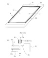
- FIG. 1 is a top view of the liquid crystal display device by Embodiment 1 of this invention
- (b) is sectional drawing
- (c) is a fragmentary sectional view which expands and shows the edge part area
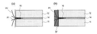
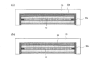
- (A) And (b) is a fragmentary sectional view which shows the structure of the liquid crystal display device of a different comparative example.
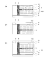
- Each of (a) to (c) is a partial cross-sectional view showing a configuration of a liquid crystal display device of a different modification.
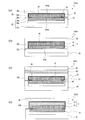
- FIG. 6 is a cross-sectional view illustrating a configuration of a liquid crystal display device according to Embodiment 2, and (a) to (d) each show another embodiment.
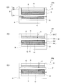
- FIG. 5 is a cross-sectional view illustrating a configuration of a liquid crystal display device according to Embodiment 2, and (a) to (c) each show another embodiment. It is sectional drawing which shows the structure of the liquid crystal display device of Embodiment 3.
- 4A and 4B are diagrams for explaining a manufacturing process of the liquid crystal display device of Embodiment 3, wherein FIG. 5A is a perspective view, and FIG. 5B is a cross-sectional view taken along line A-A ′ of FIG. It is a figure for demonstrating the manufacturing process of the liquid crystal display device of Embodiment 3, (a) is sectional drawing which shows the mode before resin filling, (b) is sectional drawing which shows the mode after resin filling. .
- FIG. 10 is a plan view for explaining a liquid crystal display device of Embodiment 5, wherein (a) is a resin on three sides of the liquid crystal panel, (b) is on two sides of the liquid crystal panel, and (c) is a resin on one side of the liquid crystal panel.
- a is a resin on three sides of the liquid crystal panel
- b is on two sides of the liquid crystal panel
- c is a resin on one side of the liquid crystal panel.
- Each of the forms in which the layers are formed is shown. It is a top view for demonstrating the display area and frame area of a liquid crystal panel.
- liquid crystal display device is used to mean various electronic devices including a liquid crystal panel.
- the “liquid crystal display device” in the present specification may be not only a display device such as a liquid crystal monitor, but also various electronic devices such as a smartphone, a tablet terminal, and a portable game machine as long as the liquid crystal panel is provided.
- the liquid crystal display device 100 includes a liquid crystal panel 10, a housing having a horizontal housing portion 20 (side wall portion) that surrounds the side end surface of the liquid crystal panel 10 with a gap G, and a resin formed from a resin material filled in the gap G. Layer 30.
- a liquid crystal panel 10 includes a pair of substrates 11 and 12 (for example, a TFT substrate 11 and a counter substrate 12) configured using glass or the like, and a liquid crystal layer held therebetween. 14. Further, a sealing material 16 is provided in an annular shape so as to surround the liquid crystal layer 14 between the pair of substrates 11 and 12. The sealing material 16 is provided for sealing the liquid crystal layer 14 between the substrates and fixing the pair of substrates 11 and 12 with respect to each other.
- an epoxy-based or acrylic-based curable resin material can be used, which is either a thermosetting type, an ultraviolet curing type, or a type that requires both ultraviolet curing and thermal curing. It may be.
- the sealing material 16 also serves to prevent the surrounding environment from affecting the liquid crystal material in the liquid crystal panel and changing the electro-optical characteristics.
- the liquid crystal panel 10 has a side end surface defined by the side end surfaces of the pair of substrates 11 and 12 and the outer surface of the sealing material 16.
- the inner side surface 20 s of the horizontal casing 20 is annularly arranged so as to surround the side end surface of the liquid crystal panel 10.
- the liquid crystal panel 10 is accommodated in a space (accommodating space) surrounded by the inner side surface 20 s of the horizontal casing 20.
- the resin layer 30 is a resin layer obtained by curing, for example, a UV (ultraviolet) curable resin material filled in the gap G between the side end surface of the liquid crystal panel 10 and the inner side surface 20 s of the horizontal casing 20. is there.
- the resin layer 30 is provided so as to cover the entire side end surface of the liquid crystal panel 10, that is, in close contact with both the end surfaces of the pair of substrates 11 and 12 and the outer surface of the sealing material 16. Yes.
- the material of the resin layer 30 will be described later, for example, a cationic polymerizable resin material is used.
- the intrusion path P1 for water vapor (or impurities) entering the liquid crystal layer 14 from the outside of the liquid crystal display device 100 has a width Pw exposed on the upper side and the lower side.
- the path is limited to a path that penetrates from the end face of the layer 30 to the inside of the resin layer 30 and further passes through the sealing material 16 to the inside of the liquid crystal layer 14. This is because the outer surface of the resin layer 30 is in close contact with and completely covered by the horizontal housing portion 20 made of a material having low moisture permeability.
- the horizontal housing part 20 is preferably formed of a material having low moisture permeability, for example, a resin such as polycarbonate or acrylic, a metal such as an aluminum alloy, a magnesium alloy, or stainless steel, or a glass or a carbon fiber composite material. Is done. Further, the thickness of the horizontal housing portion 20 is desirably as thin as possible for narrowing the frame, but is set to 0.1 mm to 1.2 mm, for example.
- FIG. 2A shows a form in which the outside of the sealing material 16 is not covered with other members.
- FIG. 2B shows a form in which only the resin layer 30 ′ covers the outside of the sealing material 16.
- the water vapor entrance path P1 is not limited, and the inside of the liquid crystal layer 14 passes through the sealing material 16 from various directions. Water vapor can enter the surface.
- FIG. 2B in the liquid crystal panel having a narrow frame, the provision of the low moisture-permeable resin layer 30 ′ outside the sealing material 16 does not restrict the water vapor entrance path P 1, which is sufficient. Moisture resistance cannot be obtained.
- water vapor can enter from the entire surface of the exposed resin, so that the time during which the inside of the resin is saturated with water vapor is shortened. Therefore, it is hardly possible to extend the time until the water vapor enters the liquid crystal panel, and the water vapor enters the liquid crystal layer 14 relatively easily.
- the exposed portion of the resin layer 30 is only the upper and lower end faces, so the area where the resin layer 30 directly touches the water vapor is Very small. Thereby, the amount of water vapor per unit time approaching the end face of the liquid crystal panel 10 can be reduced. Further, in the resin layer 30, a water vapor intrusion path P ⁇ b> 1 formed between the outside and the liquid crystal panel 10 is narrow and long. Therefore, the same effect as widening the seal width of the liquid crystal panel 10 can be obtained.
- Such a configuration is preferably applied to a narrow frame liquid crystal display device.
- the width of the sealing material 16 is set to, for example, 1.0 mm or less, and even when the resin layer 30 is provided, the thickness thereof is set to, for example, 0.8 mm or less. ing.
- the configuration in which the resin layer 30 and the horizontal housing portion 20 are disposed in close contact with the outside of the sealing material 16 as described above is to prevent the entry of water vapor and impurities into the liquid crystal layer 14. It is particularly effective.
- the liquid crystal display device 100 it is not necessary to design a wide frame area. This is because there is a gap of about 0.1 mm to 0.3 mm required for the assembly margin between the casing and the liquid crystal panel 10, and the resin may be sealed in the gap. In this manner, the liquid crystal display device 100 can improve moisture resistance while realizing a narrow frame.
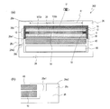
- FIGS. 3A to 3C shows a liquid crystal display device according to a modification of the present embodiment, and shows a portion corresponding to the portion shown in FIG.
- the side end face of the liquid crystal panel 10 including the outer end face of the sealing material 16 has the resin layer 30 and the horizontal casing portion arranged outside the same as in the embodiment shown in FIG. And 20. Furthermore, in this modification, a transparent casing (transparent cover) 22 is provided so as to cover the back surface 10S1 of the liquid crystal panel 10. The transparent casing 22 further covers the end faces of the horizontal casing portion 20 and the resin layer 30. The liquid crystal panel 10 and the transparent casing 22 are fixed by an interposed transparent resin layer 32.
- the modification shown in FIG. 3B is different from the modification shown in FIG. 3A in that a transparent casing 24 is provided on the surface 10S2 of the liquid crystal panel 10.
- the transparent casing 24 further covers the end faces of the horizontal casing portion 20 and the resin layer 30.
- the liquid crystal panel 10 and the transparent casing 24 are fixed by an interposed transparent resin layer 34.
- the modification shown in FIG. 3C is different from the modification shown in FIG. 3A in that transparent casings 22 and 24 are provided on both sides of the back surface 10S1 and the front surface 10S2 of the liquid crystal panel 10, respectively. .
- the transparent casings 22 and 24 also cover the end faces of the horizontal casing portion 20 and the resin layer 30, and the liquid crystal panel 10 and the transparent casings 22 and 24 are fixed by the transparent resin layers 32 and 34.
- the entry path of water vapor into the liquid crystal panel is further limited. Accordingly, it is possible to further suppress the deterioration of display quality in the peripheral display area of the liquid crystal panel 10.
- the resin layer 30 is desirably formed of a material having a lower moisture permeability than the sealing material 16 in order to enhance the moisture-proof effect.
- a polymer material having a high degree of polymerization obtained by ionic polymerization, particularly cationic polymerization is desirable to use.
- a polymer material having an epoxy component (glycidyl group) as a main component and having an epoxy component amount of at least 50 wt% or more, desirably 65 wt% or more is used.
- the above cationic polymerizable low moisture-permeable resin material may not be preferably used as the sealing material 16 of the liquid crystal panel 10. This is because if the cation used for the polymerization enters the liquid crystal, the retention rate is remarkably lowered and the transmittance is lowered, which may cause display defects such as black spots. For this reason, the material of the sealing material 16 and the material of the resin layer 30 may be formed from different materials.
- Table 1 below shows the results of a stain generation test performed on each of the liquid crystal display devices shown in FIG. 1C and FIGS. 3A to 3C.
- these liquid crystal display devices were housed in a high-temperature and high-humidity tank maintained at a temperature of 60 ° C. and a humidity of 90 ° C., and an aging test was performed.
- Table 1 also shows experimental results for a panel without moisture-proof measures (hereinafter referred to as a reference) shown as a comparative example in FIG.
- photocationic polymerization initiator for example, a boronate, onium salt, sulfonium / borate salt having boronic acid as a counter anion can be used.
- epoxy resin those having an aliphatic cyclic skeleton and / or those having an aromatic skeleton are preferable.
- aromatic skeleton include a bisphenol skeleton, a biphenyl skeleton, a naphthalene skeleton, and an anthracene skeleton.
- Examples of the cationic photopolymerization initiator and the epoxy resin are described in JP2007-46035A, JP2012-151109A, JP2011-225773A, JP49333751A, and JP2006-299034A. Has been.
- the liquid crystal display device including a backlight 40 that makes light incident on the liquid crystal panel 10.
- the liquid crystal panel 10 is a transmissive liquid crystal panel, and the liquid crystal panel 10 and the backlight 40 are typically fixed with respect to each other to form a laminated structure (panel structure).
- the liquid crystal panel 10 and the backlight 40 are accommodated in an accommodation space formed by combining the upper casing 26 and the lower casing 28.
- the liquid crystal display device 200a shown in FIG. 4A includes a thin plate-like flat plate portion 26a and an upper housing 26 including a wall-like horizontal housing portion 26b that protrudes in a substantially vertical direction from the peripheral edge of the flat plate portion 26a, and a flat plate portion 28a. And a lower housing 28 including a wall-like lateral housing portion 28b protruding in a substantially vertical direction from the peripheral edge portion of the flat plate portion 28a.
- a recessed space (accommodating space) is defined that is surrounded by the inner side surface of the horizontal housing portion 26b and the inner surface of the flat plate portion 26a.
- a concave space (accommodating space) surrounded by the inner side surface of the horizontal housing portion 28b and the inner surface of the flat plate portion 28a is defined.
- the upper housing 26 and the lower housing 28 are connected to each other at the end surfaces 26e and 28e of the horizontal housing portions 26b and 28b.
- the respective accommodation spaces are continuous. In this configuration, one storage space is formed inside the connected upper and lower casings 26 and 28.
- the liquid crystal panel 10 is accommodated in the accommodating space of the upper casing 26.
- the upper casing 26 is made of a translucent material, and is configured so that the user can observe the light emitted from the display surface 10Sb of the liquid crystal panel 10.
- the backlight 40 is accommodated in the accommodation space of the lower housing 26, and light can be emitted from the backlight 40 toward the liquid crystal panel 10.
- the horizontal casing portion 26b of the upper casing 26 surrounds the side end surface of the liquid crystal panel 10 with a slight gap, and the flat plate portion 26a sandwiches the surface of the liquid crystal panel 10 with a slight gap. Covering.
- a transparent resin layer 30 is filled in a gap between the upper casing 26 and the liquid crystal panel 10.
- the liquid crystal panel 10 is housed and fixed in the housing space of the upper housing part 26 by an intervening resin layer 30.
- the intrusion of water vapor into the liquid crystal layer is suitably prevented.
- liquid crystal panel 10 and the backlight 40 are bonded together by a double-sided tape 39, for example.
- the backlight 40 is affixed to the back surface of the liquid crystal panel 10 after the liquid crystal panel 10 is fixed in the accommodation space of the upper housing 26 using the resin layer 30.
- the lower casing 28 is fixed to the upper casing 26 so as to protect the backlight 40 in the accommodation space after fixing the backlight 40 to the liquid crystal panel 10.
- the surface 10Sa on the backlight 40 side (that is, the surface close to the end surface 26e of the horizontal housing portion 26b) is substantially the same level as the end surface 26e of the horizontal housing portion 26b. (Horizontal position). Although this will be described in detail in the third embodiment below, when the back surface of the liquid crystal panel 10 and the horizontal housing portion end surface 26e are aligned, the gap formed between the liquid crystal panel 10 and the upper housing 26 is reached. This is because it is easy to appropriately fill the resin.
- the configuration of the liquid crystal display device 200b shown in FIG. 4B will be described.
- the liquid crystal panel 10 and the backlight 40 are laminated, and these constitute the panel structure 5.
- the panel structure 5 is fixed in the accommodating space of the upper housing 26 via the resin layer 30.
- the backlight 40 and the liquid crystal panel 10 are firmly adhered to each other in advance with a double-sided tape or the like before being accommodated and fixed in the upper casing 26.
- the side end face of the liquid crystal panel 10 is covered with the resin layer 30 and the horizontal casing 26b. For this reason, invasion of water vapor into the liquid crystal layer is suitably prevented.
- the resin layer 30 can be appropriately provided in the gap.
- the liquid crystal display device 200c has a configuration in which a touch panel 50 and a cover glass 52 are provided on the user side surface of the liquid crystal display device 200a shown in FIG.
- the touch panel 50 and the cover glass 52 are attached to the outer surface of the upper housing 26 with a double-sided tape or resin.
- the liquid crystal panel 10 is fixed in the accommodation space of the upper casing 26 via the resin layer 30, and the penetration of water vapor into the liquid crystal layer is prevented by the resin layer 30 and the upper casing 26. .
- the touch panel 50 and the liquid crystal panel 10 are stacked, and these constitute the panel structure 5.
- the panel structure 5 is fixed in the accommodating space of the upper housing 26 via the resin layer 30.
- a backlight 40 is provided on the back side of the panel structure 5, and these are attached by a double-sided tape 39.
- the panel structure 5 is a panel-like structure (for example, a panel laminate) that includes at least the liquid crystal panel 10 and is accommodated in the accommodation space of the upper casing 26.
- the backlight 40 is provided on the back surface of the liquid crystal panel 10, but the backlight 40 is disposed in the accommodating space of the lower housing 28, and thus included in the panel structure 5.
- the side end face of the liquid crystal panel 10 is covered with the resin layer 30 and the horizontal casing portion 26b of the casing 26. For this reason, invasion of water vapor into the liquid crystal layer is suitably prevented.
- the resin layer 30 is used. Appropriately provided.
- the upper casing 26 encloses the liquid crystal panel 10 and the touch panel 50 with resin, and the cover glass 52 shown in FIG.
- the upper casing portion 26 has an end face 26e of a horizontal casing portion 26b extending in the vertical direction from the flat plate portion 26a (here, the bottom casing portion 26a), and is external to the liquid crystal display device 200e. It is provided to be released toward the side. Further, the flat plate portion 26a of the upper housing portion 26 is disposed on the inner side of the liquid crystal display device 200e.
- a panel structure composed of a laminated structure of the cover glass 52, the touch panel 50, and the liquid crystal panel 10 is accommodated in the accommodation space of the upper housing 26.
- the lower housing 28 is fixed to the back surface of the flat plate portion 26a of the upper housing 26 in a state in which the backlight 40 is accommodated.
- the backlight 40 may be attached to the back surface of the flat plate portion 26 a of the upper housing 26 by the double-sided tape 39.
- the back surface of the liquid crystal panel 10 is fixed to the flat plate portion 26a by the resin layer 30, and the side end surface of the liquid crystal panel 10 is fixed to the horizontal housing portion 26b by the resin layer 30.
- the touch panel 50 and the cover glass 52 are affixed on the surface (observer side surface) of the liquid crystal panel 10 with a double-sided tape or a resin.
- the horizontal housing portion 26b may be observed, and the appearance may be deteriorated.
- the mechanical strength can be improved.
- the upper housing 26 has a configuration in which a flat plate portion 26a is provided between the lower lateral housing portion 26b1 and the upper lateral housing portion 26b2.
- the liquid crystal display device 200f corresponds to a configuration in which the upper horizontal casing portion 26b2 for protecting the side end surfaces of the cover glass 52 and the touch panel 50 is provided in the upper casing 26 of the liquid crystal display device 200c shown in FIG. To do.
- the liquid crystal panel 10 is fixed to the accommodation space of the upper housing 26 via the resin layer 30 as in the liquid crystal display device 200c shown in FIG.
- the backlight 40 is affixed to the liquid crystal panel 10 with a double-sided tape 39 or the like, and is accommodated in the lower casing 28.
- the flat plate portion 26a of the upper housing 26 in the liquid crystal display device 200f shown in FIG. 5B is replaced with a transparent flat plate 27 which is another constituent member.
- the transparent flat plate 27 is joined to the inner side surface of the horizontal housing portion 26 at the intermediate portion in the thickness direction of the horizontal housing portion 26.
- Such an upper casing 26 can be manufactured by, for example, a two-color molding method in which different materials such as resin and glass are integrated.
- the transparent flat plate 27 for example, a thin glass plate or a resin plate can be used, whereby the entire apparatus can be thinned.
- the upper casing 26 is typically formed by injection molding.
- the thickness t1 of the flat plate portion 26a is about 0.5 mm at the minimum. It is often set to.
- a thin transparent flat plate 27 made of glass or the like can be used, and the thickness t2 can be set to about 0.1 mm, for example.
- FIG. 6 shows a cross section of a liquid crystal display device 300 having a configuration similar to that of the liquid crystal display device 200a shown in FIG.
- the same referential mark is attached
- the liquid crystal display device 300 includes the liquid crystal panel 10 disposed in the housing space of the upper housing 26, and the backlight 40 and the circuit board 60 disposed in the housing space of the lower housing 28.
- the circuit board 60 may be provided with various signal processing circuits, drive circuits, power supplies, and the like, and is typically electrically connected to the liquid crystal panel 10 and the backlight 40.
- the liquid crystal panel 10 is housed and fixed in the housing space of the upper housing 26 via the resin layer 30.
- the resin layer 30 only needs to be provided at least in the gap between the side end face of the liquid crystal panel 10 and the horizontal casing 26b, and is necessarily provided so as to cover the display surface 10Sb of the liquid crystal panel 10. It does not have to be done.
- At least a region (substantially the entire flat plate portion 26a) corresponding to the display region R1 of the liquid crystal panel 10 in the upper housing 26 has translucency and is typically transparent.
- the resin layer 30 disposed between the display surface 10Sb of the liquid crystal panel 10 and the upper housing 26 is also translucent and is typically transparent. Thereby, the user U can observe the display surface 10Sb of the liquid crystal panel 10.
- the liquid crystal panel 10 includes a TFT substrate 11 and a counter substrate 12, and a liquid crystal layer 14 surrounded by a sealing material 16 is sealed therebetween.
- a region surrounded by a boundary between the sealing material 16 and the liquid crystal layer 14 (an inner edge of the sealing material 16) is defined as a display region R1.
- the TFT substrate 11 is provided with a plurality of TFTs and a plurality of pixel electrodes connected thereto, and the counter substrate 12 is provided with a color filter and a black matrix.
- the liquid crystal panel 10 may be in various display modes.
- the counter substrate 12 is provided with a counter electrode and ribs and slits for regulating the alignment direction of liquid crystal molecules.
- a common electrode is provided on the TFT substrate 11 so as to face the pixel electrode with an insulating layer interposed therebetween.
- the configuration of the liquid crystal panel 10 may be a known one.
- optical film layers 18 and 19 are provided on the backlight side surface (back surface) 10Sa and the user side surface (display surface) 10Sb of the liquid crystal panel 10, respectively.
- the optical film layers 18 and 19 are, for example, a pair of polarizing films arranged in crossed Nicols so that their transmission axes are orthogonal to each other.
- the present invention is not limited to this, and the optical film layers 18 and 19 may be a light diffusion film, a retardation film, or the like.
- the optical film layers 18 and 19 may be a laminate of a plurality of optical films having the above functions.
- the liquid crystal panel 10 is disposed in the recessed space of the upper housing 26 with a slight gap G therebetween.
- the liquid crystal panel 10 is arranged such that the display surface 10Sb faces the flat plate portion 26a of the upper casing 26 (that is, the bottom surface of the housing space).
- the width d2 of the gap G formed between the liquid crystal panel 10 and the horizontal casing 26b is set to 0.1 mm to 0.3 mm, for example.
- the gap width d2 may be determined according to the processing accuracy of the liquid crystal panel 10 and the upper housing 26, the assembly margin, and the like.
- the gap width d2 corresponds to the thickness of the resin layer 30 that covers the side end surface of the liquid crystal panel 10.
- a transparent resin material can be used. More specifically, as described in Embodiment 1, for example, a cationic polymerization resin can be used. Further, as the transparent resin material, for example, XET manufactured by Mitsui Chemicals, Inc. can be used.
- the inner diameter of the nozzle 90 used in the dispenser device is preferably less than the gap width d2. The reason is that when the inner diameter of the nozzle 90 is equal to or larger than the gap width d2, the discharged resin material protrudes from the gap and may not be applied neatly.
- the width 26t ( The width of the region near the edge of the upper housing 26 adjacent to the liquid crystal panel 10 is preferably set to at least 0.3 mm from the corner. Considering stable mass production, the width 26t is more preferably 0.5 mm or more.
- the dispenser nozzle for example, various nozzles available from ACE-GIKEN Co., Ltd. can be used.
- the optical film layer 18 is affixed on the back surface 10Sa of the liquid crystal panel 10 as shown in FIG. 6 (In addition, in FIG.7 (b), this optical film layer 18 is included. Is shown as the liquid crystal panel 10).
- the housing space of the upper housing 26 is relative to the liquid crystal panel 10 so that the back surface 10Sa of the liquid crystal panel 10 (that is, the outer surface of the optical film layer 18) and the end surface 26e of the upper housing 26 are substantially aligned. Is provided.
- casing 26 has the further housing part outside the end surface 26e, and the end surface is also formed in this part.
- the end surface 26e of the horizontal casing portion 26b is a surface having a spread in the in-plane direction of the liquid crystal panel 10, and means a surface formed at a position closest to the liquid crystal panel 10. To do.
- a step (distance in the normal direction of the panel) between the end face 26e of the horizontal casing 26b and the surface of the liquid crystal panel 10 (or a panel structure including the liquid crystal panel).
- Is d1 the smaller the step d1, the easier it is to properly fill the resin with the dispenser device.
- the level difference d1 does not substantially exist, and one surface of the liquid crystal panel 10 and the horizontal housing part end surface 26e are positioned at substantially the same level.
- step difference d1 is 0.05 mm or less, and includes the case where a slight level
- the needle 90 of the dispenser device is set to an appropriate height without contacting the liquid crystal panel 10 or the upper housing 26, and the resin is placed at a desired position without interruption. Can be encapsulated.
- the step d1 is preferably smaller than the gap width d2 (that is, d1 ⁇ d2).
- the gap width d2 is generally set to about 0.1 mm to 0.3 mm in consideration of processing accuracy and assembly tolerance of the casing and the liquid crystal panel. Therefore, the level difference d1 is preferably less than 0.1 mm, and more preferably 0.05 mm or less.
- the resin material can be appropriately filled in the gap by the dispenser device.
- the filled resin is preferably cured immediately by an optimal curing method depending on the type of resin, such as heat or ultraviolet rays. By doing so, the end face of the liquid crystal panel 10 can be tightly sealed, and impurities, moisture, and the like can be prevented from entering the liquid crystal layer.
- FIG. 9A shows a mode in which the side end surface of the liquid crystal panel 10 and the display surface of the liquid crystal panel 10 are housed and fixed at once in the housing space of the upper housing 26 with resin.
- the resin layer 30a covering the side end surface of the liquid crystal panel 10 and the resin layer 30b covering the display surface of the liquid crystal panel 10 are formed in the same process of injecting and curing the resin.
- a resin layer 30a that covers only the side end face of the liquid crystal panel 10 may be formed by filling the gap between the liquid crystal panel 10 and the resin.
- FIG. 10 is a cross-sectional view illustrating a configuration of a liquid crystal display device 302 according to a modification.
- the liquid crystal display device 302 is different from the liquid crystal display device 300 shown in FIG. 6 in that a wall-like portion that further protrudes from an end surface 26e1 that defines a housing space for housing the liquid crystal panel 10 in the horizontal housing portion 26b of the upper substrate 26. 26c.
- the lower housing 28 is also provided with a wall-like portion 28c so as to be properly fitted with the wall-like portion 26c.
- the liquid crystal panel 10 (including the optical films 18 and 19) is housed inside the upper housing 26 by the resin layer 30 so that there is no step with the end surface 26e1 of the lateral housing portion 26b.
- the backlight 40 is attached to the liquid crystal panel 10 held on the upper housing 26 by the resin layer 30 with a double-sided tape or the like.
- the end surface of the backlight 40 is surrounded by the wall-shaped portion 26c protruding from the end surface 26e1, and thereby the backlight 40 is protected. Therefore, after attaching the backlight 40 to the liquid crystal panel 10, a mechanical impact is applied to the backlight 40 in a later manufacturing process (for example, a process of connecting the upper casing 26 and the lower casing 28). In this case, it is possible to reduce the possibility that the backlight 40 is peeled off from the liquid crystal panel 10 and to prevent problems in the manufacturing process.
- the end surface 26e2 of the wall portion 26c is positioned higher than the surface of the backlight 40 attached to the liquid crystal panel 10. It is preferable to be formed.
- FIGS. 11A and 11B show a mode in which the liquid crystal panel 10 is fixed in the housing space of the lower housing 28.
- the above-described backlight, circuit board, etc. may be disposed between the liquid crystal panel 10 and the bottom surface of the lower casing 28.
- a resin material is filled in a gap between the side end surface of the liquid crystal panel 10 and the inner side surface of the horizontal housing portion 28b of the lower housing 28, and the formed resin layer 30 causes the liquid crystal panel 10 to be placed on the lower side. It is fixed in the housing space of the housing 28.
- the resin material is poured into the gap using the dispenser device 55.
- the needle attached to the tip of the dispenser device 55 moves directly above the gap between the lower housing 28 and the liquid crystal panel 10.
- the needle of the dispenser device 55 be as close as possible to the liquid crystal panel 10 or the lower housing 28 in order to inject the resin without interruption.
- the resin layer 30 can be suitably formed by substantially equalizing the height of the casing near the resin and the liquid crystal panel (or panel structure). .
- the liquid crystal panel 10 is a liquid crystal panel that does not require a polarizing plate, such as a PDLC (Polymer Dispersed Liquid Crystal) mode, and does not have other members such as a touch panel
- the liquid crystal panel 10 It is preferable that the surface of the substrate to be configured and the end surface of the horizontal frame portion are aligned.
- the polarizing plate is affixed on the liquid crystal panel 10, it is preferable to arrange
- the resin material for forming the resin layer 30 may be the same material as the sealing material 16 (see FIG. 1) provided in the liquid crystal panel 10 (for example, Sekisui Chemical Co., Ltd. Photorec S series). Curable resins (Loctite [Henkel Japan Co., Ltd.], Photorec [Sekisui Chemical Co., Ltd.], etc.), epoxy thermosetting resins (Mitsui Chemicals Co., Ltd.) good.
- the above materials can be used not only in Embodiment 4 but also in Embodiments 1 to 3 described above.
- FIGS. 12A and 12B show a form in which translucent covers 58 and 59 covering the entire liquid crystal panel 10 are provided on the surface of the lower casing 28 in which the liquid crystal panel 10 is accommodated.
- the translucent cover 58 has a lens portion 58a having a curved surface at least at the peripheral edge thereof.
- the lens unit 58a enlarges the image in the peripheral display area of the liquid crystal panel 10 and thereby displays the image so that the image also exists on the frame area. Thereby, the liquid crystal display device which does not seem to have a frame can be provided.
- the translucent cover 58 having such a lens portion is described more specifically in, for example, International Publication No. 2010-089998 filed by the present applicant.
- International Publication No. 2010-089998 filed by the present applicant.
- the entire disclosure of International Publication No. 2010-089998 is incorporated herein by reference.
- the lens part of the translucent cover 59 covers up to the mold part of the resin layer 30.
- a connection portion 59 ′ for connecting the lens portion and the lower housing 28 is provided in the vicinity of the end surface of the lower housing 28.
- the frame is difficult to be visually recognized.
- the area where the light emitted from the display area of the liquid crystal panel 10 should be enlarged is small, so that the lens portion and the translucent cover 59 are made thinner. Can do.
- the connection portion 59 ′ for connecting the translucent cover 59 and the lower housing 28 is provided at a position hidden from the lens portion when viewed by the user, so that the frame is conspicuous by the connection portion 59 ′. Is also prevented.
- FIGS. 13A and 13B a transparent upper side having a lens portion similar to the translucent cover 58 shown in FIG. 12A and having an accommodation space inside.
- You may comprise a liquid crystal display device using the housing 26.
- FIG. 13 (a) the liquid crystal panel 10 is fixed to the accommodation space of the transparent upper casing 26 via the resin layer 30, and then the lower casing 28 is shown in FIG. 13 (b).
- the resin layer 30 is provided not only on the side end face of the liquid crystal panel 10 but also on the front side, it is preferable to form the resin layer 30 by applying a transparent resin material in a vacuum.
- FIGS. 14A to 14C show a configuration in which the resin layer 30 is not provided on at least one of the four sides of the liquid crystal panel 10.
- the resin layer 30 is not necessarily provided for all four sides of the liquid crystal panel 10. For example, when a wide frame region is provided on any side of the liquid crystal panel 10, moisture resistance can be improved by increasing the width of the sealing material, and thus the resin layer 30 may not be provided. . That is, only the side of the four sides of the liquid crystal panel 10 that needs to have a very narrow frame may be protected by providing the resin layer 30.
- FIG. 14A shows a form in which the resin layer 30 is provided on the three sides of the upper side, the left side, and the right side, and the resin layer 30 is not provided on the lower side.
- a terminal portion is provided on the lower side, and there are few merits of thinning the frame until the sealing material 16 of the liquid crystal panel 10 is thinned. Therefore, on the lower side where the terminal portion is located, the sealing material 16 is sufficiently thick, for example, the frame is set to about 2 mm or more, and the resin layer 30 is formed only on the three sides that realize the other narrow frame.
- FIG. 14B shows a form in which the resin layer 30 is provided on the left side and the right side, and the resin layer 30 is not provided on the upper side and the lower side.
- an earpiece, a camera, a light receiving unit, and the like may be provided at the upper part of the liquid crystal panel 10
- an operation button and a mouthpiece may be provided at the lower part.
- the effect of narrowing the frame of the liquid crystal panel by narrowing the sealing material is at most less than about 1 mm.
- the frame of the liquid crystal panel 10 is thinned only on the left and right sides and protected by the resin layer 30.
- the upper and lower sides may have a sufficiently wide seal width, for example, the frame may be set to 2 mm or more so that the reliability of the liquid crystal panel 10 can be maintained even if the resin layer 30 is not present.
- FIG. 14C shows a case where two liquid crystal panels 10 are arranged adjacent to each other and only a frame region formed between them is a narrow frame.
- the resin layer 30 may be provided only on one side where a narrow frame is required.
- pixels are driven by TFTs (oxide semiconductor TFTs) that use an oxide semiconductor layer as an active layer. Also good.
- the oxide semiconductor TFT is provided for each pixel as a switching element on the TFT substrate.
- the oxide semiconductor layer includes, for example, an In—Ga—Zn—O-based semiconductor (hereinafter abbreviated as “In—Ga—Zn—O-based semiconductor”).
- a TFT having an In—Ga—Zn—O-based semiconductor layer has high mobility (more than 20 times that of an a-Si TFT) and low leakage current (less than one hundredth of that of an a-Si TFT). It is suitably used as a drive TFT and a pixel TFT.
- a TFT having an In—Ga—Zn—O-based semiconductor layer is used, power consumption of the display device can be significantly reduced.
- the In—Ga—Zn—O-based semiconductor may be amorphous, may include a crystalline portion, and may have crystallinity.
- a crystalline In—Ga—Zn—O-based semiconductor in which the c-axis is oriented substantially perpendicular to the layer surface is preferable.
- Such a crystal structure of an In—Ga—Zn—O-based semiconductor is disclosed in, for example, Japanese Patent Laid-Open No. 2012-134475. For reference, the entire disclosure of Japanese Patent Application Laid-Open No. 2012-134475 is incorporated herein by reference.
- the oxide semiconductor layer may include another oxide semiconductor instead of the In—Ga—Zn—O-based semiconductor.
- Zn—O based semiconductor ZnO
- In—Zn—O based semiconductor IZO (registered trademark)
- Zn—Ti—O based semiconductor ZTO
- Cd—Ge—O based semiconductor Cd—Pb—O based
- CdO cadmium oxide
- Mg—Zn—O based semiconductors In—Sn—Zn—O based semiconductors (eg, In 2 O 3 —SnO 2 —ZnO), In—Ga—Sn—O based semiconductors, etc. You may go out.
- a casing including a horizontal casing portion having an inner side surface, a housing provided with a housing space surrounded by the inner side surface, a pair of substrates, a liquid crystal layer held between the pair of substrates, and the A panel structure including a liquid crystal panel provided with a sealing material provided so as to surround a liquid crystal layer, the panel structure being accommodated in the accommodation space, the inner side surface of the horizontal casing, and the liquid crystal panel A resin layer that fills at least a part of a gap formed between the side end surface and fixes the liquid crystal panel to the inner surface, and in the in-plane direction of the liquid crystal panel, the liquid crystal panel A liquid crystal display device, wherein a sealing material is covered with the resin layer and the horizontal housing portion.
- liquid crystal display device of item 1 even in a narrow frame liquid crystal display device, it is preferable to prevent water vapor and impurities from the outside from entering the liquid crystal layer, and thereby display defects in the peripheral display region Can be prevented.
- liquid crystal display device of item 2 it is possible to effectively prevent water vapor and the like from entering the liquid crystal layer.
- the horizontal casing portion has an end surface that is continuous with the inner side surface and substantially orthogonal to the inner side surface, and the panel structure and the liquid crystal panel are respectively provided on the end surface of the horizontal casing portion.
- the resin can be appropriately filled in the gap between the liquid crystal panel and the casing and a suitable resin layer can be formed, it is effective for intrusion of water vapor or the like into the liquid crystal layer. Can be prevented.
- liquid crystal display device of item 4 since a suitable resin layer can be formed, it is possible to effectively prevent water vapor and the like from entering the liquid crystal layer.
- liquid crystal display device of item 5 since a suitable resin layer can be formed even when the gap is narrow, it is possible to effectively prevent water vapor and the like from entering the liquid crystal layer.
- liquid crystal display device of item 6 since a suitable resin layer can be formed, it is possible to effectively prevent intrusion of water vapor or the like into the liquid crystal layer.
- liquid crystal display device of item 7 since a suitable resin layer can be formed, it is possible to effectively prevent water vapor and the like from entering the liquid crystal layer.
- the frame area becomes more difficult to see.
- the panel structure has a planar rectangular shape having four sides, and the inner side surface of the horizontal casing portion is formed so as to surround the four sides. 10.
- the resin layer can be provided only on the side where a narrow frame is required.
- the casing includes a flat plate portion that is connected to the horizontal casing portion and forms a bottom surface of the housing space, and the resin layer made of the same material as the resin layer includes the panel structure and the flat plate portion.
- the liquid crystal display device according to any one of items 1 to 10, which is also formed in a gap between the two.
- the panel structure can be more securely fixed to the housing by the resin layer.
- a separate housing including a horizontal housing portion having a housing inner side surface, and a housing space surrounded by the inner side surface, and a backlight is held in the housing space of the separate housing.
- the liquid crystal panel and the backlight can be stacked and accommodated in the accommodation space formed by combining the two casing portions.
- the embodiment of the present invention is widely used as various liquid crystal display devices including a liquid crystal panel.
Landscapes
- Physics & Mathematics (AREA)
- Nonlinear Science (AREA)
- Mathematical Physics (AREA)
- Chemical & Material Sciences (AREA)
- Crystallography & Structural Chemistry (AREA)
- General Physics & Mathematics (AREA)
- Optics & Photonics (AREA)
- Liquid Crystal (AREA)
Abstract
Description
図1(a)~(c)は、本発明の実施形態1による液晶表示装置100の構成を示す。液晶表示装置100は、液晶パネル10と、液晶パネル10の側端面を間隙Gを空けて囲う横筺体部20(側壁部)を有する筺体と、間隙Gに充填された樹脂材料から形成される樹脂層30とを有している。

以下、実施形態2の液晶表示装置として、液晶パネル10に光を入射するバックライト40を備える液晶表示装置について種々の態様を説明する。本実施形態において、液晶パネル10は透過型の液晶パネルであり、液晶パネル10とバックライト40とは、典型的には、互いに対して固定され、積層構造(パネル構造体)を構成する。
実施形態3では、上側筺体26または下側筺体28が有する凹空間内に、液晶パネル10やこれを含むパネル構造体を樹脂層30を介して収容する際の収容形態について説明する。
図11(a)および(b)は、下側筺体28の収容空間に液晶パネル10を固定する形態を示す。なお、図11(a)には示していないが、前述のバックライトや回路基板などが、液晶パネル10と下側筺体28の底面との間に配置されていても良いことは言うまでもない。
図14(a)~(c)は、液晶パネル10の4辺のうちの少なくとも1辺において、樹脂層30を設けない構成を示す。
11 TFT基板
12 対向基板
14 液晶層
16 シール材
18、19 光学フィルム層
20 横筺体部
26 上側筺体
26a 平板部
26b 横筺体部
26e 横筺体部の端面
28 下側筺体
30 樹脂層
40 バックライト
50 タッチパネル
58、59 レンズ部付き透光性カバー
60 回路基板
100 液晶表示装置
R1 表示領域
R1a 周辺表示領域
R2 額縁領域
R3 シール領域
Claims (12)
- 内側側面を有する横筺体部を備え、前記内側側面によって囲まれた収容空間が設けられている筺体と、
一対の基板、および、前記一対の基板間に保持された液晶層および前記液晶層を囲むように設けられたシール材を備えた液晶パネルを含むパネル構造体であって、前記収容空間に収容されるパネル構造体と、
前記横筺体部の前記内側側面と前記液晶パネルの側端面との間に形成された隙間の少なくとも一部に充填され、前記内側表面に対して前記液晶パネルを固定する樹脂層と
を備え、
前記液晶パネルの面内方向において、前記液晶パネルの前記シール材が、前記樹脂層および前記横筺体部によって覆われている、液晶表示装置。 - 前記樹脂層は、前記一対の基板の側端面を含む、前記液晶パネルの側端面の全体を覆う、請求項1に記載の液晶表示装置。
- 前記横筺体部は、前記内側側面に連続し、前記内側側面と略直交する端面を有しており、
前記パネル構造体および液晶パネルは、それぞれ、前記横筺体部の前記端面に近い側の第1表面と、前記第1表面とは反対側の第2表面とを有しており、
前記液晶パネルの法線方向における前記横筺体部の前記端面と、前記パネル構造体または前記液晶パネルの前記第1表面との段差d1が、0mm以上0.1mm以下である請求項1または2に記載の液晶表示装置。 - 前記段差d1は、前記内側側面と前記液晶パネルの側端面との間の隙間の幅d2よりも小さい、請求項3に記載の液晶表示装置。
- 前記隙間の幅d2は、0.1mm以上0.3mm以下である、請求項3または4に記載の液晶表示装置。
- 前記樹脂層は、カチオン重合性の樹脂材料から形成される、請求項1から5のいずれかに記載の液晶表示装置。
- 前記シール材は、前記樹脂層とは異なる材料から形成されている、請求項6に記載の液晶表示装置。
- 前記シール材の幅が1.0mm以下である、請求項7に記載の液晶表示装置。
- 前記パネル構造体の周縁部分に対応する位置にレンズ部を有し、前記パネル構造体を覆うように設けられた透光性カバーをさらに備える、請求項1から8のいずれかに記載の液晶表示装置。
- 前記パネル構造体は、4辺を有する平面矩形状の形状を有し、前記横筺体部の前記内側側面は、前記4辺を囲むように形成されており、前記4辺のうちの3辺、2辺または1辺に対応する箇所にのみ、前記樹脂層が形成されている、請求項1から9のいずれかに記載の液晶表示装置。
- 前記筺体は、前記横筺体部に接続され前記収容空間の底面を形成する平板部を有し、
前記樹脂層と同じ材料からなる樹脂層が、前記パネル構造体と前記平板部との間の隙間にも形成されている、請求項1から10のいずれかに記載の液晶表示装置。 - 内側側面を有する横筺体部を含み、前記内側側面によって囲まれた収容空間が設けられている別筺体をさらに有し、前記別筺体の収容空間には、バックライトが保持されており、前記筺体と前記別筺体とは、それぞれの横筺体部の端面同士が接合するように接続されており、前記液晶パネルと前記バックライトとが積層されている、請求項1から11のいずれかに記載の液晶表示装置。
Priority Applications (2)
| Application Number | Priority Date | Filing Date | Title |
|---|---|---|---|
| CN201480042168.7A CN105408808B (zh) | 2013-07-26 | 2014-07-25 | 液晶显示装置 |
| US14/907,366 US9798174B2 (en) | 2013-07-26 | 2014-07-25 | Liquid crystal display apparatus |
Applications Claiming Priority (2)
| Application Number | Priority Date | Filing Date | Title |
|---|---|---|---|
| JP2013-155785 | 2013-07-26 | ||
| JP2013155785 | 2013-07-26 |
Publications (1)
| Publication Number | Publication Date |
|---|---|
| WO2015012388A1 true WO2015012388A1 (ja) | 2015-01-29 |
Family
ID=52393420
Family Applications (1)
| Application Number | Title | Priority Date | Filing Date |
|---|---|---|---|
| PCT/JP2014/069691 Ceased WO2015012388A1 (ja) | 2013-07-26 | 2014-07-25 | 液晶表示装置 |
Country Status (3)
| Country | Link |
|---|---|
| US (1) | US9798174B2 (ja) |
| CN (1) | CN105408808B (ja) |
| WO (1) | WO2015012388A1 (ja) |
Families Citing this family (4)
| Publication number | Priority date | Publication date | Assignee | Title |
|---|---|---|---|---|
| KR20170098351A (ko) * | 2016-02-19 | 2017-08-30 | 삼성디스플레이 주식회사 | 표시 장치 |
| CN108105725A (zh) * | 2018-01-02 | 2018-06-01 | 京东方科技集团股份有限公司 | 一种背光模组及显示装置 |
| CN108227265A (zh) * | 2018-01-18 | 2018-06-29 | 深圳市志凌伟业技术股份有限公司 | 一种具粗化结构之触控面板 |
| KR20200098177A (ko) * | 2019-02-12 | 2020-08-20 | 현대자동차주식회사 | 차량용 디스플레이장치 |
Citations (4)
| Publication number | Priority date | Publication date | Assignee | Title |
|---|---|---|---|---|
| JPH06123882A (ja) * | 1992-10-13 | 1994-05-06 | Sony Corp | 液晶表示装置 |
| JP2009103857A (ja) * | 2007-10-23 | 2009-05-14 | Citizen Holdings Co Ltd | 液晶装置 |
| JP2010037517A (ja) * | 2008-08-08 | 2010-02-18 | Dic Corp | 液晶パネルの画像表示部とその保護基材との接着用カチオン重合性樹脂組成物、液晶ディスプレイ及びその製造方法 |
| WO2010089998A1 (ja) * | 2009-02-06 | 2010-08-12 | シャープ株式会社 | 表示装置 |
Family Cites Families (18)
| Publication number | Priority date | Publication date | Assignee | Title |
|---|---|---|---|---|
| JPH10123964A (ja) * | 1996-08-30 | 1998-05-15 | Sony Corp | 液晶表示装置 |
| JP4933751B2 (ja) | 2004-06-23 | 2012-05-16 | 積水化学工業株式会社 | 有機エレクトロルミネッセンス素子封止剤、及び、有機エレクトロルミネッセンス素子 |
| JP4452683B2 (ja) | 2005-01-26 | 2010-04-21 | 積水化学工業株式会社 | 有機エレクトロルミネッセンス素子用封止剤、有機エレクトロルミネッセンス表示装置の製造方法、及び、有機エレクトロルミネッセンス表示装置 |
| JP2006267532A (ja) | 2005-03-24 | 2006-10-05 | Citizen Watch Co Ltd | シール部材及びそれを用いた液晶装置 |
| JP2006299034A (ja) | 2005-04-19 | 2006-11-02 | Sekisui Chem Co Ltd | 光カチオン重合性組成物 |
| JP2007065523A (ja) * | 2005-09-02 | 2007-03-15 | Hitachi Displays Ltd | 表示パネル及び表示装置とこれを備える機器 |
| JP4483833B2 (ja) * | 2005-09-22 | 2010-06-16 | エプソンイメージングデバイス株式会社 | 電気光学装置、電子機器、保護部材、保護部材の製造方法 |
| JP4575486B2 (ja) * | 2007-10-24 | 2010-11-04 | セイコーインスツル株式会社 | 表示装置 |
| JP5121432B2 (ja) | 2007-12-11 | 2013-01-16 | キヤノン株式会社 | 液晶表示装置及びその製造方法並びに液晶プロジェクション装置 |
| CN101883829A (zh) * | 2007-12-14 | 2010-11-10 | 夏普株式会社 | 粘合片和显示装置 |
| JP5268761B2 (ja) * | 2008-05-26 | 2013-08-21 | 三菱電機株式会社 | 表示装置およびその製造方法 |
| JP5555532B2 (ja) | 2010-04-22 | 2014-07-23 | 積水化学工業株式会社 | 有機el素子用封止剤及び有機el素子 |
| KR101720151B1 (ko) * | 2010-09-13 | 2017-03-28 | 삼성디스플레이 주식회사 | 액정 표시 장치 |
| WO2012042787A1 (ja) * | 2010-09-27 | 2012-04-05 | シャープ株式会社 | 液晶モジュール及び電子機器 |
| CN103339715B (zh) | 2010-12-03 | 2016-01-13 | 株式会社半导体能源研究所 | 氧化物半导体膜以及半导体装置 |
| JP6014325B2 (ja) | 2010-12-28 | 2016-10-25 | 積水化学工業株式会社 | 有機エレクトロルミネッセンス表示素子用封止剤 |
| EP2804046B1 (en) * | 2011-07-27 | 2016-10-19 | LG Display Co., Ltd. | Display device and method of fabricating the same |
| KR101507503B1 (ko) * | 2012-05-29 | 2015-03-31 | 엘지디스플레이 주식회사 | 디스플레이 장치 |
-
2014
- 2014-07-25 CN CN201480042168.7A patent/CN105408808B/zh active Active
- 2014-07-25 WO PCT/JP2014/069691 patent/WO2015012388A1/ja not_active Ceased
- 2014-07-25 US US14/907,366 patent/US9798174B2/en not_active Expired - Fee Related
Patent Citations (4)
| Publication number | Priority date | Publication date | Assignee | Title |
|---|---|---|---|---|
| JPH06123882A (ja) * | 1992-10-13 | 1994-05-06 | Sony Corp | 液晶表示装置 |
| JP2009103857A (ja) * | 2007-10-23 | 2009-05-14 | Citizen Holdings Co Ltd | 液晶装置 |
| JP2010037517A (ja) * | 2008-08-08 | 2010-02-18 | Dic Corp | 液晶パネルの画像表示部とその保護基材との接着用カチオン重合性樹脂組成物、液晶ディスプレイ及びその製造方法 |
| WO2010089998A1 (ja) * | 2009-02-06 | 2010-08-12 | シャープ株式会社 | 表示装置 |
Also Published As
| Publication number | Publication date |
|---|---|
| US20160178957A1 (en) | 2016-06-23 |
| US9798174B2 (en) | 2017-10-24 |
| CN105408808B (zh) | 2018-09-14 |
| CN105408808A (zh) | 2016-03-16 |
Similar Documents
| Publication | Publication Date | Title |
|---|---|---|
| JP5717326B2 (ja) | 液晶装置、電子機器、液晶装置の製造方法 | |
| US10502997B2 (en) | Touch liquid crystal display device with two adhesives, touch display device and lamination method | |
| CN103792734B (zh) | 显示装置以及显示器 | |
| CN104749841B (zh) | 薄膜晶体管阵列基板及其制造方法 | |
| US20160178943A1 (en) | Liquid crystal display panel | |
| US9733507B2 (en) | Display device and manufacturing method of display device | |
| JP6895318B2 (ja) | 表示装置 | |
| US20220250014A1 (en) | Display device | |
| US9581857B2 (en) | Display device and manufacturing method of the same | |
| WO2015012388A1 (ja) | 液晶表示装置 | |
| US10012863B2 (en) | Liquid crystal display device | |
| TWI480592B (zh) | 具有黑色條紋之圖案化相位延遲型顯示裝置及其製造方法 | |
| US20170176802A1 (en) | Liquid crystal display device | |
| US10048534B2 (en) | Display device | |
| US9182633B2 (en) | Display device and display apparatus having particular barrier wall structure | |
| KR20150102249A (ko) | 투명 표시 장치 및 이의 제조 방법 | |
| US20150160510A1 (en) | Liquid crystal display device | |
| US9459486B2 (en) | Liquid crystal display device in which display of off state reflected light is suppressed | |
| JP2011082098A (ja) | 有機el装置、電気光学装置及び電子機器 | |
| JP2009163081A (ja) | 液晶装置及びその製造方法 | |
| CN118244527A (zh) | 3d影像显示用有源延迟器和显示装置 | |
| KR102784884B1 (ko) | 액정표시장치 | |
| WO2012046442A1 (ja) | 液晶表示装置 | |
| JP2009058620A (ja) | 電気光学装置及び電子機器 | |
| JP2008242193A (ja) | 液晶表示素子 |
Legal Events
| Date | Code | Title | Description |
|---|---|---|---|
| WWE | Wipo information: entry into national phase |
Ref document number: 201480042168.7 Country of ref document: CN |
|
| 121 | Ep: the epo has been informed by wipo that ep was designated in this application |
Ref document number: 14829344 Country of ref document: EP Kind code of ref document: A1 |
|
| WWE | Wipo information: entry into national phase |
Ref document number: 14907366 Country of ref document: US |
|
| NENP | Non-entry into the national phase |
Ref country code: DE |
|
| NENP | Non-entry into the national phase |
Ref country code: JP |
|
| 122 | Ep: pct application non-entry in european phase |
Ref document number: 14829344 Country of ref document: EP Kind code of ref document: A1 |