WO2015011848A1 - 変位計測装置及び変位計測方法 - Google Patents
変位計測装置及び変位計測方法 Download PDFInfo
- Publication number
- WO2015011848A1 WO2015011848A1 PCT/JP2013/083291 JP2013083291W WO2015011848A1 WO 2015011848 A1 WO2015011848 A1 WO 2015011848A1 JP 2013083291 W JP2013083291 W JP 2013083291W WO 2015011848 A1 WO2015011848 A1 WO 2015011848A1
- Authority
- WO
- WIPO (PCT)
- Prior art keywords
- diffraction grating
- light
- displacement
- displacement measuring
- measuring device
- Prior art date
- Legal status (The legal status is an assumption and is not a legal conclusion. Google has not performed a legal analysis and makes no representation as to the accuracy of the status listed.)
- Ceased
Links
Images










Classifications
-
- G—PHYSICS
- G01—MEASURING; TESTING
- G01D—MEASURING NOT SPECIALLY ADAPTED FOR A SPECIFIC VARIABLE; ARRANGEMENTS FOR MEASURING TWO OR MORE VARIABLES NOT COVERED IN A SINGLE OTHER SUBCLASS; TARIFF METERING APPARATUS; MEASURING OR TESTING NOT OTHERWISE PROVIDED FOR
- G01D5/00—Mechanical means for transferring the output of a sensing member; Means for converting the output of a sensing member to another variable where the form or nature of the sensing member does not constrain the means for converting; Transducers not specially adapted for a specific variable
- G01D5/26—Mechanical means for transferring the output of a sensing member; Means for converting the output of a sensing member to another variable where the form or nature of the sensing member does not constrain the means for converting; Transducers not specially adapted for a specific variable characterised by optical transfer means, i.e. using infrared, visible, or ultraviolet light
- G01D5/266—Mechanical means for transferring the output of a sensing member; Means for converting the output of a sensing member to another variable where the form or nature of the sensing member does not constrain the means for converting; Transducers not specially adapted for a specific variable characterised by optical transfer means, i.e. using infrared, visible, or ultraviolet light by interferometric means
-
- G—PHYSICS
- G01—MEASURING; TESTING
- G01D—MEASURING NOT SPECIALLY ADAPTED FOR A SPECIFIC VARIABLE; ARRANGEMENTS FOR MEASURING TWO OR MORE VARIABLES NOT COVERED IN A SINGLE OTHER SUBCLASS; TARIFF METERING APPARATUS; MEASURING OR TESTING NOT OTHERWISE PROVIDED FOR
- G01D5/00—Mechanical means for transferring the output of a sensing member; Means for converting the output of a sensing member to another variable where the form or nature of the sensing member does not constrain the means for converting; Transducers not specially adapted for a specific variable
- G01D5/26—Mechanical means for transferring the output of a sensing member; Means for converting the output of a sensing member to another variable where the form or nature of the sensing member does not constrain the means for converting; Transducers not specially adapted for a specific variable characterised by optical transfer means, i.e. using infrared, visible, or ultraviolet light
- G01D5/32—Mechanical means for transferring the output of a sensing member; Means for converting the output of a sensing member to another variable where the form or nature of the sensing member does not constrain the means for converting; Transducers not specially adapted for a specific variable characterised by optical transfer means, i.e. using infrared, visible, or ultraviolet light with attenuation or whole or partial obturation of beams of light
- G01D5/34—Mechanical means for transferring the output of a sensing member; Means for converting the output of a sensing member to another variable where the form or nature of the sensing member does not constrain the means for converting; Transducers not specially adapted for a specific variable characterised by optical transfer means, i.e. using infrared, visible, or ultraviolet light with attenuation or whole or partial obturation of beams of light the beams of light being detected by photocells
- G01D5/36—Forming the light into pulses
- G01D5/38—Forming the light into pulses by diffraction gratings
-
- G—PHYSICS
- G01—MEASURING; TESTING
- G01M—TESTING STATIC OR DYNAMIC BALANCE OF MACHINES OR STRUCTURES; TESTING OF STRUCTURES OR APPARATUS, NOT OTHERWISE PROVIDED FOR
- G01M11/00—Testing of optical apparatus; Testing structures by optical methods not otherwise provided for
- G01M11/08—Testing mechanical properties
Definitions
- the present invention relates to a displacement measuring apparatus and a displacement measuring method using optical interference.
- Patent Document 1 discloses a displacement measuring device using optical interference.
- This displacement measuring device includes a laser light source, a collimator lens, a first diffraction grating, a second diffraction grating, and an optical sensor in this order from the light source side.
- the optical sensor diffracted light (for example, 1st order) diffracted by the first diffraction grating and diffracted light (for example, 1st order) generated by diffracting the 0th order light traveling straight through the first diffraction grating with the second diffracted light.
- the interference light is detected.
- This displacement measuring device measures a change in the distance between the first and second diffraction gratings, that is, a displacement to be measured based on a change in the amount of light due to the brightness of the interference light detected by the optical sensor (for example, patent document). 1 specification paragraphs [0020], [0023], [0027], see FIGS. 1 to 3).
- the optical encoder described in Patent Document 2 includes a first slit plate, a second slit plate facing the first slit plate, and a detector that works in conjunction with the second slit plate.
- the slit pitch of the second slit plate is smaller than the slit pitch of the first slit plate.
- the detector detects the light transmitted through both the slits of the first and second slit plates, and generates a pulse signal corresponding to this detection. Occurs (see, for example, paragraph [0011] of Patent Document 2 and FIG. 3).
- the displacement measuring device described in Patent Document 1 measures the relative displacement of these diffraction gratings in the direction along the optical axis of the two diffraction gratings.
- the optical path difference between the two lights constituting the interference light increases.
- the coherence of the light source decreases the amplitude of the interference light, that is, attenuates the amplitude. That is, there is a problem that the detection range becomes narrower as the distance between the diffraction gratings becomes larger.
- An object of the present invention is to provide a displacement measuring device and a displacement measuring method capable of suppressing the detection range from becoming narrow.
- a displacement measuring apparatus includes a light source, a first diffraction grating, a second diffraction grating, an optical sensor, and arithmetic processing means.
- the first diffraction grating and the second diffraction grating are disposed along the path of the light beam from the light source, are relatively movable, and generate diffracted light, respectively.
- the optical sensor includes a ⁇ n-order diffracted light generated from the second diffraction grating when + n-order diffracted light (n is a natural number of 1 or more) from the first diffraction grating is incident on the second diffraction grating;
- the -n-order diffracted light from the first diffraction grating is incident on the second diffraction grating, and the interference light with the + n-order diffracted light generated from the second diffraction grating is detected.
- the arithmetic processing means based on the signal obtained by the optical sensor, in the direction perpendicular to the optical axis of the first diffraction grating and the second diffraction grating, the first diffraction grating and the second diffraction grating The relative displacement of the diffraction grating is calculated.
- the light from the light source enters the first diffraction grating and the second diffraction grating which are arranged along the path of the light beam from the light source and are relatively movable. Generating diffracted light from each of the first diffraction grating and the second diffraction grating.
- the relative relationship between the first diffraction grating and the second diffraction grating in the direction orthogonal to the optical axes of the first diffraction grating and the second diffraction grating is calculated.
- FIG. 1 is a diagram schematically showing a configuration of a basic optical system of a displacement measuring apparatus according to the first embodiment of the present invention.
- FIG. 2 is a graph showing the relationship between the relative displacement amount of the diffraction grating pair in the x direction and the voltage signal obtained by the PD.
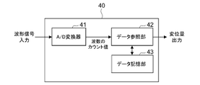
- FIG. 3 is a block diagram showing a functional configuration of the arithmetic circuit.
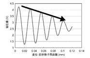
- FIG. 4 shows an example in which the amplitude of the interference light decreases as the distance between the diffraction gratings increases in the optical system shown in the prior art document 1.
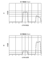
- FIGS. 5A and 5B show the intensity distributions of signals obtained by the PD when the distance between the diffraction gratings is intentionally changed.
- FIGS. 5A and 5B show the intensity distributions of signals obtained by the PD when the distance between the diffraction gratings is intentionally changed.
- FIGS. 7A to 7D respectively show simulations of signals obtained by the PD in accordance with the optical path difference of the light constituting the interference light on the optical axis of the diffraction grating pair.
- FIG. 8 is a block diagram illustrating a functional configuration of the arithmetic circuit according to the second embodiment.
- FIG. 9 shows the relationship between the relative displacement in the x direction of the diffraction grating pair and the voltage signal obtained by the PD.
- FIG. 10 is a schematic perspective view showing the configuration of the displacement measuring apparatus according to the third embodiment of the present invention.
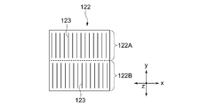
- FIG. 11 shows the configuration of the second diffraction grating according to the third embodiment.
- FIG. 12 is a block diagram illustrating a functional configuration of the arithmetic circuit according to the third embodiment.
- FIG. 13 shows signals obtained in the y 1 light receiving area A and the y 2 light receiving area of the PD.
- FIG. 14 shows the second diffraction grating viewed in the z direction, out of the diffraction grating pair of the displacement measuring apparatus according to the fourth embodiment of the present invention.
- FIG. 15 shows the light receiving area of the PD viewed in the z direction in this displacement measuring apparatus.
- FIG. 16 shows waveform signals respectively obtained from the four light receiving areas.
- FIG. 17 is a block diagram showing a functional configuration of an arithmetic circuit of the displacement measuring device.
- FIG. 18 is a block diagram showing a functional configuration of an arithmetic circuit of a displacement measuring apparatus according to the fifth embodiment of the present invention.
- FIGS. 19A to 19D show simulations of three waveform signals obtained in each light receiving region of the PD for each of different intensities of the zero-order light included in the interference light.
- FIG. 20 shows an embodiment of a displacement measuring device including a holding mechanism for holding the optical system shown in FIG. 1, for example.
- the displacement measuring apparatus does not measure the displacement of the diffraction grating pair in the direction along the optical axis, but relatively displaces the diffraction grating pair in a direction perpendicular to it.
- the problem of a decrease in amplitude does not occur. Accordingly, problems such as a narrow detection range can be solved.
- the first diffraction grating and the second diffraction grating may each have a plurality of grating lines, and the arithmetic processing unit may calculate the displacement along the arrangement direction of the plurality of grating lines.
- the amount of interference light obtained by the optical sensor changes according to the relative displacement of the first and second diffraction gratings in the arrangement direction of the plurality of grating lines. Therefore, the arithmetic processing means can calculate the displacement in the arrangement direction.
- the optical sensor receives the zero-order light that travels straight along the optical axis through the first diffraction grating and the second diffraction grating, so that the ⁇ n-order diffracted light generated by the second diffraction grating and The interference light with the 0th-order light may be detected. Between the first diffraction grating and the second diffraction grating so that an optical path difference between the ⁇ nth order diffracted light and the zeroth order light satisfies (2m + 1) ⁇ / 4 (m is an integer of 0 or more). The distance may be set. Thereby, since the optical sensor receives interference light with as low light intensity as possible, noise due to zero-order light can be suppressed.
- the arithmetic processing means may include a detection value output unit that outputs a detection value of a waveform signal obtained by the optical sensor and having a periodicity corresponding to the lattice line pitch.
- the detection value output unit may have a predetermined detection level set so that the arithmetic processing means outputs displacement at intervals smaller than the grid line pitch. Thereby, the arithmetic processing means can output the displacement at an interval smaller than the grid line pitch.
- Either one of the first diffraction grating and the second diffraction grating may have a plurality of shift regions configured by being divided.
- the plurality of shift regions may have lattice line patterns that are shifted from each other by a predetermined distance smaller than 1 ⁇ 2 of the lattice line pitch in the arrangement direction of the plurality of lattice lines.
- the optical sensor may include a plurality of light receiving regions that receive the light emitted from the plurality of shift regions. Thereby, the phase of the signal obtained in each light receiving region can be shifted.
- the arithmetic processing means may selectively switch signals obtained in the plurality of light receiving regions at a predetermined timing, and use the selected one signal for the arithmetic processing. Depending on the waveform shape of the signal obtained in the light receiving region, there is a signal region in which the detection sensitivity with respect to the change in the displacement amount is low. By selectively switching a signal to be processed at a predetermined timing, it is not necessary to set a signal region having a low detection sensitivity as a processing target, and measurement accuracy is improved.
- the arithmetic processing means may include a detection value output unit and a switching unit.
- the detection value output unit may output a detection value of a waveform signal having periodicity according to the lattice line pitch, which is obtained in each of the plurality of light receiving regions.
- the switching unit may switch the processing target to the second waveform signal at a timing of detecting a predetermined detection value smaller than the amplitude peak value of the first waveform signal to be processed among the waveform signals.
- the arithmetic processing means processes, as the predetermined detection value, a detection value at the intersection of the first waveform signal and the second waveform signal or a detection value at the same level as the detection value at the intersection. May be.
- the arithmetic processing means includes a count unit that counts the intersections of waveform signals each obtained in the plurality of light receiving regions and having periodicity according to the grid line pitch, and based on the count value by the count unit, The displacement may be calculated. Since the intersection obtained from each waveform signal increases in accordance with the displacement, the arithmetic processing means can measure the displacement by counting the intersection.
- the arithmetic processing means has a counting unit that counts the intersections of the waveform signals obtained in the plurality of light receiving regions, each having a periodicity corresponding to the lattice line pitch, and the average value of the waveform signals.
- the displacement may be calculated based on a count value by the count unit.
- the displacement measuring apparatus includes: a first holder that holds the light source and the first diffraction grating; a second holder that holds the second diffraction grating and the optical sensor unit; the first holder; You may further comprise the connection part which connects the said 2nd holder so that relative movement is possible along the direction orthogonal to the said optical axis.
- FIG. 1 is a diagram schematically showing a configuration of a basic optical system of a displacement measuring apparatus according to the first embodiment of the present invention.
- the displacement measuring apparatus 100 includes a light source 12, a collimator lens 14, a diffraction grating pair 20, a PD (Photo Detector) 31 that is an optical sensor, and an arithmetic circuit 40.
- the light source 12 is an LD (Laser Diode) or an LED (Light Emitting Diode), and is driven by a driver (not shown).
- LD Laser Diode
- LED Light Emitting Diode
- the collimator lens 14 turns the light emitted from the light source 12 into parallel light 15. At least the light source 12 and the collimator lens 14 constitute an optical system that generates parallel light.
- the diffraction grating pair 20 includes, for example, a transmission type first diffraction grating 21 and second diffraction grating 22.
- the first diffraction grating 21 and the second diffraction grating 22 are arranged so as to face each other along the paths of the light beams from the light source 12 and the collimator lens 14, here along the optical axes of the light source 12 and the collimator lens 14. As described later, it is relatively movable in a predetermined direction.
- the first diffraction grating 21 includes the incident parallel light 15 that travels straight on the optical axis of the diffraction grating pair 20 and the 0th order light 30a and + nth order diffracted light (n is a natural number of 1 or more, and so on). ) 23a and -n-order diffracted light 25a.
- the second diffraction grating 22 emits the 0th-order light 30a emitted from the first diffraction grating 21 and incident on the second diffraction grating 22 as 0th-order light 30b that travels straight on the optical axis. Further, the second diffraction grating 22 generates a ⁇ n-order diffracted light 23b of the + n-order diffracted light 23a incident thereon, and generates a + n-order diffracted light 25b of the ⁇ n-order diffracted light 25a incident thereon.
- the order of diffracted light generated from one light beam and bent to the right side of the one light beam is positive. Further, the order of the diffracted light that is bent to the left of the one light beam is negative.
- the ⁇ nth order diffracted light 23b and the + nth order diffracted light 25b interfere with each other, and the interference light 27 is generated.
- the PD 31 is disposed at a position where the interference light 27 is mainly detected. Specifically, the ⁇ nth order diffracted light 23b and the + nth order diffracted light 25b travel in a direction along the optical axis of the diffraction grating pair 20 (z direction in FIG. 1), and the interference light 27 is generated at a position including the optical axis. To do. Accordingly, the PD 31 that detects the interference light 27 is disposed on the optical axis of the diffraction grating 20.
- the light on the optical axis also includes the 0th-order light 30, and the interference light including the 0th-order light 30 is referred to as interference light 28 for convenience of explanation.
- ⁇ 1st order diffracted light is typically used as ⁇ nth order diffracted light.
- ⁇ 2nd order and subsequent diffracted light is used. It may be used. In practice, there are many diffracted lights other than those shown in FIG. 1, but they are not shown for ease of explanation.
- the diffracted lights of both the + nth order diffracted light 23a and the ⁇ nth order diffracted light 23b are hereinafter referred to as the first diffracted light 23 as necessary.
- the diffracted light of both the ⁇ nth order diffracted light 25a and the + nth order diffracted light 25b is hereinafter referred to as the second diffracted light 25 as necessary.
- the 0th-order light of both the 0th-order lights 30a and 30b is hereinafter referred to as 0th-order light 30.
- the first diffraction grating 21 and the second diffraction grating 22 have substantially the same shape and the same size.
- the diffraction grating 21 (and 22) has a plurality of grating lines 21a (and 22a) which are grooves along the y direction orthogonal to the z direction in FIG.
- the pitch P of the grating lines 21a of the first diffraction grating 21 and the pitch P of the grating lines 22a of the second diffraction grating 21 are formed substantially the same.
- the pitch P is 3.3 ⁇ m and the groove depth is 473 ⁇ m. Of course, it is not restricted to these values.
- the displacement measuring apparatus 100 uses the relative displacement ⁇ x of the diffraction grating pair 20 in the x direction, which is the arrangement direction of the grating lines 21a and 22a, as a measurement target.
- the measurable range is, for example, a submicrometer to micrometer order displacement.
- two axes orthogonal to the z direction are defined as x and y axes.
- the direction along the grating lines 21a and 22a of each diffraction grating is the y direction
- the arrangement direction of the grating lines 21a and 22a is the x direction.
- the second diffraction grating 22 and the PD 31 are integrally held, and can move integrally in the x direction with respect to the first diffraction grating 21.
- the arithmetic circuit 40 mainly functioning as arithmetic processing means calculates a displacement ⁇ x by performing predetermined arithmetic processing based on a signal obtained by the PD 31.
- the arithmetic circuit 40 mainly includes hardware such as an MPU (Micro Processing Unit), a RAM (Random Access Memory), and a ROM (Read Only Memory).
- the arithmetic circuit 40 may include a PLD (Programmable Logic Device) such as an FPGA (Field Programmable Gate Array) in addition to or instead of the MPU, or a DSP (Digital Signal Processor), ASIC. (Application Specific Integrated Circuit) or the like may be provided.
- the arithmetic circuit 40 may be configured by a plurality of physically separated chip packages or elements.
- FIG. 2 is a graph showing the relationship between the relative displacement ( ⁇ m) in the x direction of the diffraction grating pair 20 and the voltage signal obtained by the PD 31.
- the pitch of the grating lines 21a and 22a of the diffraction grating pair 20 is, for example, 3.3 ⁇ m
- the center wavelength of the light from the light source 12 is 850 nm.
- the PD 31 outputs a waveform signal having periodicity for each pitch P of the lattice lines 21a and 22a. That is, for each pitch P, the PD 31 obtains an amount of light with one set of light and dark sets of the grid lines as one cycle.
- the waveform signal having periodicity is typically a sin waveform signal.
- FIG. 3 is a block diagram showing a functional configuration of the arithmetic circuit 40.
- the arithmetic circuit 40 mainly includes an A / D converter 41, a data reference unit 42, and a data storage unit 43.
- the A / D converter 41 functions as a detection value output unit that converts the analog signal output from the PD 31 into a digital value and outputs the digital value.
- the A / D converter 41 counts the number of waves of the input signal, for example, by counting the frequency of the waveform signal, and outputs this count value.
- the data storage unit 43 is a lookup table that correlates the wave value (corresponding to the count value) of the waveform signal detected by the PD 31 by the relative movement of the diffraction grating pair 20 and the relative displacement amount of the diffraction grating pair 20. Store the data.
- the table data is stored in the memory when the displacement measuring apparatus 100 is manufactured.
- the data reference unit 42 extracts a displacement amount corresponding to the count value of the wave number counted by the A / D converter 41 from the data storage unit 43, and outputs this. That is, the arithmetic circuit 40 can measure the amount of displacement in units of the pitch of the grating lines 21a and 22a of each diffraction grating.
- the signal value obtained by the PD 31 is 0, and the relative displacement amount of the diffraction grating pair 20 is 0.
- the form and arrangement of the PD 31, the circuit of the arithmetic circuit 40 and the program thereof are designed.
- the arithmetic circuit 40 may have a reset function that sets the amount of displacement at the reference position of the diffraction grating pair 20 to zero. This is effective as a calibration method when, for example, the displacement value output from the arithmetic circuit 40 at the reference position of the diffraction grating pair 20 does not become zero due to a change with time of the displacement measuring apparatus 100.
- the arithmetic circuit 40 may have a function of updating the table data in the data storage unit 43 using the information at the time of calibration.
- the displacement measuring apparatus 100 does not measure the displacement of the diffraction grating pair 20 in the direction along the optical axis, but relatively displaces the diffraction grating pair 20 in the direction orthogonal thereto. Measure the displacement. Accordingly, in principle, the amplitude of the interference light decreases as the distance between the diffraction gratings 21 and 22 increases (see, for example, FIG. 4: the horizontal axis of the graph in FIG. 4 indicates the distance between the diffraction gratings, that is, the distance in the z direction). This does not happen. Therefore, problems such as a narrow detection range can be solved.
- the path lengths (optical path lengths) of the first diffracted light 23 and the second diffracted light 25 are substantially the same, that is, no optical path difference occurs. Therefore, even if the distance between the diffraction gratings 21 and 22 varies, the amplitude of the interference light is not affected, and an appropriate amplitude of the interference light can be obtained.
- FIG. 5A shows the intensity distribution of a signal obtained by the PD 31 when the distance between the diffraction gratings 21 and 22 is 15 ⁇ m
- FIG. 5B shows the signal obtained by the PD 31 when the distance is 23 ⁇ m. That is, the value on the vertical axis indicates the light intensity that is the output value of the optical sensor, the horizontal axis indicates the position (mm) in the x direction shown in FIG. 1, and the position through which the optical axis passes is 0 mm.
- FIGS. 6A and 6B show the signal intensity obtained by the second PD when another interference light is detected by the second PD arranged at a position shifted from the optical axis of the diffraction grating pair 20.
- the distribution is shown (intensity distribution on the right side of the graph), and the intensity distribution of the signal obtained from the optical axis PD on the optical axis is shown (intensity distribution in the center in the graph).
- the different interference lights are the first order diffracted light generated from the second diffraction grating when the 0th order light from the first diffraction grating enters the second diffraction grating, and the first order diffracted light from the first diffraction grating is the first order diffracted light.
- This is interference light with zero-order light that is incident on the second diffraction grating and is generated from the second diffraction grating (see FIG. 1 of Patent Document 1).
- the light receiving area of the second PD is arranged at a position of approximately 3 to 5 mm.
- the PD 31 receives not only the interference light 27 but also the zero-order light 30 that travels straight along the optical axis of the diffraction grating pair 20. That is, in practice, the PD 31 receives three light interference lights 28 (see FIG. 1) of the first diffracted light 23, the second diffracted light 25, and the 0th-order light 30. However, the 0th-order light 30 is basically unnecessary for the measurement process of the displacement ⁇ x, and the 0th-order light appears as noise in the output signal of the PD 31.
- the distance between the diffraction gratings 21 and 22 (distance in the z direction) is set to a predetermined distance in order to suppress the generation of noise due to the zero-order light 30.
- the distance is such that the optical path difference between the three light beams of the zero-order light, the first diffracted light 23 and the second diffracted light 25 constituting the interference light 28 is (2m + 1) ⁇ / 4 (m is an integer of 0 or more) ).
- the optical path difference does not substantially occur in the first diffracted light 23 and the second diffracted light 25, the zero-order light and the first diffracted light 23 (or the second diffracted light 23 (or the second diffracted light 23) are substantially not generated.
- the optical path difference with the diffracted light 25) may satisfy the above formula.
- the arrangement of the first diffraction grating 21 and the second diffraction grating 22 is set so that the optical path differences are 0.25 ⁇ , 0.75 ⁇ , 1.25 ⁇ ,.
- the PD 31 receives the interference light 28 having a light intensity as low as possible, which suppresses noise caused by the zero-order light. Means.
- a waveform indicated by a broken line indicates that another interference light is generated by a PD (the second PD) arranged at a position shifted from the optical axis according to the relative displacement of the diffraction grating pair. This is a waveform when detected.
- the other interference light is the + 1st order diffracted light generated from the second diffraction grating when the 0th order light from the first diffraction grating is incident on the second diffraction grating, and the first diffraction grating.
- + 1st order diffracted light is incident on the second diffraction grating and is interference light with 0th order light generated from the second diffraction grating (see FIG. 1 of Patent Document 1).
- the PD 31 can obtain a waveform signal having a periodicity of an appropriate shape.
- FIGS. 7B and 7D when the optical path difference is 0.5 ⁇ and ⁇ , a signal having high light intensity but including noise due to zero-order light is obtained.
- the A / D converter 41 counts the wave number of the waveform signal, but it may output one count for each half wavelength by detecting the upper peak and the lower peak.
- the displacement measuring apparatus can measure the displacement with a resolution (for example, 1.65 ⁇ m) half of the lattice line pitch (for example, 3.3 ⁇ m).
- the same members, functions, etc. included in the displacement measuring apparatus 100 according to the embodiment shown in FIG. 1 and the like will not be described or will be mainly described.
- the principle of generation of interference light by the diffraction grating pair is the same as that in the first embodiment.
- the structure of the displacement measuring apparatus 100 shown in FIG. 1 is typically used.
- FIG. 8 is a block diagram showing a functional configuration of the arithmetic circuit according to the second embodiment.
- FIG. 9 shows the relationship between the relative displacement ( ⁇ m) in the x direction of the diffraction grating pair 20 and the voltage signal obtained by the PD 31, and is a graph having a scale smaller than the horizontal axis of the graph of FIG. is there.
- the vertical axis of the graph of FIG. 9 is normalized with the overall amplitude of the voltage waveform signal set to 1 so that the lightness (or intensity) of the interference light, which is the amount of light received by the PD 31, is 1 and maximum.
- the arithmetic circuit 140 divides the overall amplitude of the vertical axis of the graph by a plurality of predetermined voltage levels (detection levels), and monitors the waveform signal at those voltage levels. That is, the A / D converter 41 has a predetermined voltage level set so that the arithmetic circuit 40 outputs displacement at intervals smaller than the grid line pitch.
- the data storage unit 43 stores the voltage level and the count value in association with the displacement amount for each divided voltage level and for each count value of the wave number. Since the waveform of the signal is not linear but a sin curve, for example, unequal voltage values are selected and stored so that the interval for each stored displacement amount is constant.
- the A / D converter 41 since two identical voltage values appear within one wavelength of the signal, the A / D converter 41 counts a wave of twice the frequency, that is, a half wavelength, as one. Output the count value. In this case, the A / D converter 41 can count the wave number by counting both the upper peak and the lower peak of the waveform signal, with one half wavelength as one. The A / D converter 41 outputs a voltage value in units of the voltage level currently being measured.
- the data reference unit 42 acquires the count value counted by the A / D converter 41 and the voltage value output from the A / D converter 41.
- the data reference unit 42 extracts a displacement amount corresponding to the acquired count value and voltage value from the data storage unit 43 and outputs this.
- the arithmetic circuit 140 can measure the displacement amount with an accuracy smaller than the pitch of the grating lines 21a and 22a of each diffraction grating, for example, a unit of 100 nm.
- the data storage unit 43 stores the voltage levels at equal intervals, and the arithmetic circuit 140 uses only the linear region of the waveform signal so as to shift at equal intervals as in a third embodiment described later. An amount may be output.
- FIG. 10 is a schematic perspective view showing the configuration of the displacement measuring apparatus according to the third embodiment of the present invention.
- FIG. 11 shows the configuration of the second diffraction grating according to the third embodiment.
- the region through which light is transmitted in the second diffraction grating 122 of the displacement measuring apparatus 200 is divided into a plurality of regions, for example, two regions 122A and 122B in the y direction. These two areas are referred to as “y 1 shift area” and “y 2 shift area” for convenience.
- the pitch of each lattice line in the y 1 shift region 122A and the y 2 shift region 122B is substantially the same.
- the grid line pattern in the y 1 shift region 122A is shifted by a predetermined distance smaller than 1 ⁇ 2 of the pitch of the grid lines 123 in the x direction with respect to the grid line pattern in the y 2 shift region 122B.
- each grid line pattern is formed at a position shifted by 1 ⁇ 4 pitch.
- the PD 33 that is the optical sensor according to the present embodiment is divided into a plurality of regions, for example, two light receiving regions 33A and 33B in the y direction so as to correspond to the plurality of regions of the second diffraction grating 122. It is configured. These light receiving areas are referred to as “y 1 light receiving area” and “y 2 light receiving area” for convenience. That is, of the interference light 27 (or 28) (see FIG. 1) emitted from the second diffraction grating 122, the light emitted from the y 1 shift region 122A enters the y 1 light receiving region 33A. Further, the light emitted from the y 2 shift region 122B enters the y 2 light receiving region 33B.
- the diffraction grating pair 120 is configured to be relatively movable in the x-axis direction.
- the second diffraction grating 122 is held so as to be movable integrally with the PD 33.
- FIG. 12 is a block diagram showing a functional configuration of the arithmetic circuit according to the present embodiment.
- a channel of a signal input to the arithmetic circuit 240 a channel to which a signal obtained in the y 1 light receiving region 33A of the PD 33 is input is channel 1 (ch.1), and a signal obtained in the y 2 light receiving region 33B is The input channel is channel 2 (ch.2).
- the arithmetic circuit 240 includes an A / D converter 41, a data reference unit 42, and a data storage unit 43 for channels 1 and 2, respectively. These blocks basically function in the same manner as each block of the arithmetic circuit 140 described in the second embodiment (see FIG. 8).
- the arithmetic circuit 240 has switches 44 and 45 for switching ON / OFF of the output from each data reference section 42, and also has an output timing control section 46 for controlling the operation of the switches 44 and 45.
- the output timing control unit 46 acquires the count value and the voltage value of each of the channels 1 and 2, and controls one of the channels 1 and 2 by controlling the operation of the switches 44 and 45 based on these values.
- the displacement amount of is output. That is, the output timing control unit 46 functions as a switching unit that switches the amount of displacement to be output (that is, an arithmetic processing target) by selectively switching the switches 44 and 45 alternately.
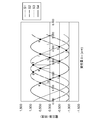
- FIG. 13 shows signals obtained from the PD 33, that is, signals obtained from the y 1 light receiving area 33A and the y 2 light receiving area 33B (first waveform signal S1 and second waveform signal S2), respectively.
- the horizontal axis is displacement
- the vertical axis is a detection value (voltage value) representing the amount of received light.
- the lattice line patterns are shifted from each other by a quarter of the lattice line pitch, so that the phases of the signals S1 and S2 are also shifted by a quarter. .
- the output timing control unit 46 when the diffraction grating pair 122 is relatively moved in the direction in which the displacement amount of the diffraction grating pair 120 is increased, the output timing control unit 46, as shown in FIG. 13, points A, B, C, D, E,. • Switch the outputs of channels 1 and 2 to each other in order. For example, the output timing control unit 46 outputs the displacement amount using the signal S2 from the points B to C (using the channel 2), and uses the signal S1 at the timing to obtain the count value and the detection value at the point C. To output the displacement amount (using channel 1).
- the switching order is in the reverse direction such as points I, H, G,.
- Points C, F, I,... are intersections of the signals S1 and S2.
- Point A is a detection value at the same level as point C
- point D is the same detection value as point F
- point G is the same detection value as point I.
- Point B shows the same amount of displacement as point A
- point E shows the same amount of displacement as point D
- point H shows the same amount of displacement as point G.
- the output timing control unit 46 switches to the signal S2 (or signal S1) and switches before reaching the peak of the signal S1 (or S2) (at a timing at which a predetermined detection value smaller than the amplitude peak value is detected).
- the later signal is set as a signal to be arithmetically processed. That is, measurement accuracy can be increased by using a linear region that is a region with good detection sensitivity among the detection values of the signals S1 and S2.
- the arithmetic circuit 240 calculates the difference between the signals S1 and S2, and sets the timing when this becomes 0 as the intersections C, F, I,. It may be the timing of.
- the shift amount of the grid line pattern is set to 1 ⁇ 4.
- any shift amount may be used as long as the shift amount is less than 1 ⁇ 2, such as 3, 5, and the like.
- the points A and C or the points D and F have the same detection values as the intersections of the signals S1 and S2, but other points other than the intersections may be set as switching timing points.
- one optical sensor has a plurality of light receiving areas, but a plurality of light receiving areas may be configured by a plurality of physically separated optical sensors.
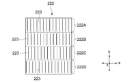
- FIG. 14 shows the second diffraction grating viewed in the z direction, out of the diffraction grating pair of the displacement measuring apparatus according to the fourth embodiment of the present invention.
- FIG. 15 shows the light receiving area of the PD viewed in the z direction in this displacement measuring apparatus.
- the second diffraction grating 222 of the diffraction grating pair of the displacement measuring apparatus has a plurality of shift regions divided into the y direction, for example, four shift regions 222A, 222B, 222C, and 222D.
- the pitches of the lattice lines 223 in these four shift regions are substantially the same.
- the lattice line patterns of the three shift regions 222A, 222B, and 222C among the four shift regions are arranged so as to be shifted from each other in the x direction by 1/6 of the lattice line pitch.
- the lattice line pattern of the other shift region 222D is one-third of the lattice line pitch with respect to the lattice line pattern of the shift regions 222A and 222C out of the three shift regions 222A, 222B, and 222C.
- the shift region 222D is referred to as a “reference shift region”.
- the arrangement of the three shift regions 222A, 222B and 222C and the reference shift region 222D in the second diffraction grating 222 is not limited.
- the reference shift region 222D may be disposed between two of the three shift regions and one other shift region.
- the light receiving area of the PD 34 corresponds to each of the shift areas 222A to 222D of the second diffraction grating 222 configured as described above, for example, a plurality of light receiving areas, for example, four light receiving areas 34A. 34D, divided in the y direction.
- the interference light 27 (or 28) (see FIG. 1) to be detected the light receiving areas 34A to 34D of the PD 34 detect light emitted from the shift areas 222A to 222D, respectively.
- the light receiving area 34D is hereinafter referred to as “reference light receiving area”.
- FIG. 16 shows waveform signals respectively obtained from these four light receiving regions.
- the phase of the waveform signal S4 obtained in the reference light receiving region 34D is shifted by 120 ° from the phase of the waveform signals S1 and S3 obtained in the light receiving regions 34A and 34C.
- the phases of the waveform signals S1 to S3 obtained in the three light receiving areas 34A to 34C are shifted from each other by 60 °.
- FIG. 17 is a block diagram showing a functional configuration of an arithmetic circuit of the displacement measuring device.
- the arithmetic circuit 340 includes a count unit 341, a data reference unit 342, and a data storage unit 343.
- Waveform signals S1 to S4 are input to the count unit 341 via channels 1 to 4.
- the counting unit 341 counts intersections of these waveform signals S1 to S4, and the arithmetic circuit 340 calculates the displacement ⁇ x based on the count value. Specifically, for example, when determining the timing of the intersection point a between the signals S4 and S1, the count unit 341 monitors the timing when the difference between the signals S4 and S1 becomes 0 (or a threshold value close to 0 or less). In this way, the counting unit 341 counts the intersections a, b, c,... K of the signals S1 to S4.
- the counting unit 341 may include an A / D converter and perform digital processing, but does not include an A / D converter, and can perform intersection counting even by analog processing.
- the data storage unit 343 stores a count value and a displacement amount in advance in association with each other.
- the data reference unit 342 extracts a displacement amount corresponding to the intersection count value output from the count unit 341 from the data storage unit 343, and outputs this as a displacement amount ⁇ x.
- a point l shown in white is not an intersection of waveform signals, but is a timing point at which the signal S1 becomes 0 at the timing next to the point k.
- the counting unit 341 also counts this point l exceptionally, and the data reference unit 342 can output a displacement corresponding to this point l. Thereby, the arithmetic circuit 340 can output the displacement amount of equal intervals.
- the arithmetic circuit 340 can output the displacement at an interval sufficiently smaller than the pitch of the grating line. That is, highly accurate displacement measurement is possible.
- the second diffraction grating may have three shift regions, and the PD may have three light receiving regions corresponding to them.
- the lattice line patterns of the three shift regions are shifted by 1/3 of the lattice line pitch in the x direction.
- the PD can output three waveform signals having phases shifted from each other by 120 ° from their light receiving regions. Then, the arithmetic circuit can acquire these three waveform signals, count their intersections, and calculate the displacement amount based on the count value.
- FIG. 18 is a block diagram showing a functional configuration of an arithmetic circuit of a displacement measuring apparatus according to the fifth embodiment of the present invention.
- the displacement measuring apparatus according to the fifth embodiment includes the second diffraction grating having three shift regions as described above, and a PD having three light receiving regions corresponding to the shift regions. Is provided.
- the arithmetic circuit 440 includes an A / D converter 41, a count unit 341, an average value calculation unit 444, a data reference unit 442, and a data storage unit 443.
- the three A / D converters 41 obtain waveform signals obtained from the three light receiving regions of the PD via the channels 1 to 3 and output digital values of the respective waveform signals.
- the average value calculation unit 444 calculates each value acquired from the A / D converter 41, that is, an average value of three waveform signals.
- the count unit 441 counts the intersections between the average value and the value forming each waveform signal acquired from the A / D converter 41, and outputs the count value.
- the data storage unit 443 stores a count value and a displacement amount in advance in association with each other.
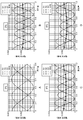
- 19A to 19D show the above 1.
- the PD detects the interference light 28 including the 0th-order light 30, for each different intensity of the 0th-order light 30 included in the interference light 28, in each light receiving region of the PD.
- a simulation of the three waveform signals obtained is shown. These graphs also show the average values of these three waveform signals.
- the ratios of the intensity of the 0th-order light 30 included in the interference light 28 are 0%, 2%, 4%, and 6%, respectively.
- the data reference unit 442 extracts a displacement amount corresponding to each of the intersection points a, b, c,... (See FIGS. 19B to 19D) counted by the count unit 441 from the data storage unit 443, and outputs this.
- each average detected by the detection level of the average value is obtained by obtaining an average value that is a line following the noise of the zero-order light.
- Waveform signal values (intersection points) appear at precise intervals in the displacement direction. Therefore, the arithmetic circuit 440 can calculate an accurate displacement based on the count values of these intersections.
- the displacement measuring apparatus forms three waveform signals. However, as in the above-described embodiment, two or more waveform signals are formed, and these waveform signals and the average value are obtained. The intersection may be counted, and the displacement may be output based on the count value.
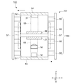
- FIG. 20 shows an embodiment of a displacement measuring device 100 (or 200) including a holding mechanism that holds the optical system shown in FIG.
- the holding mechanism 50 includes a box-shaped first holder 51 and second holder 52.
- the first holder 51 integrally supports the light source 12, the collimator lens 14, and the first diffraction grating 21.
- the second holder 52 integrally supports the second diffraction grating 22 and the PD 31.
- a mounting substrate 53 on which the light source 12 is mounted is attached to one end of the first holder 51.
- the first diffraction grating 21 is attached to the other end of the second holder 52.
- the second diffraction grating 22 is attached to one end of the second holder 52, and the mounting substrate 54 on which the PD 31 is mounted is attached to the other end of the second holder 52.
- the first holder 51 is formed with a passage 58 through which light emitted from the light source 12 enters the first diffraction grating 21 via the collimator lens 14.
- the second holder 52 is formed with a passage 59 for the interference light 27 (see FIG. 1) emitted from the second diffraction grating 22 to mainly enter the PD 31.
- the holding mechanism 50 includes a support mechanism 150 that supports the first holder 51 and the second holder 52 so as to be slidable in the x direction.
- the support mechanism 150 functions as a connection portion that connects the holders 51 and 52 so as to be relatively movable in the x direction.
- the support mechanism 150 includes a slide shaft 55 that extends in the x direction.
- a through hole in the x direction (not shown) is formed at the bottom (lower part in the y direction in the figure) of the first holder 51 and the second holder 52, and the slide shaft 55 is inserted into the through hole.
- two slide shafts 55 are provided in one holder.
- the support mechanism 150 includes an elastic member 57 that elastically connects the first holder 51 and the second holder 52.
- the elastic member 57 is provided, for example, so as to connect the side surfaces of the first holder 51 and the second holder 52, and is provided, for example, on both side surfaces.
- the elastic member 57 has a structure or shape that can be elastically deformed mainly by resin, metal, or the like.
- the first holder 51 is fixed to a first part (not shown) of the measurement object, and the second holder 52 is attached to a second part (not shown) of the measurement object.
- This displacement measuring device 100 is attached to the measurement object so that is fixed. Thereby, the displacement of the x direction of the 1st and 2nd site
- the arithmetic circuit basically outputs a displacement by referring to a lookup table that associates a count value (and voltage level) with a displacement amount.
- the arithmetic circuit may output the displacement using a predetermined arithmetic expression.
- the arithmetic circuit stores a predetermined unit displacement amount and multiplies the count value by the unit displacement amount, or adds the unit displacement amount every time the count value is obtained. For example, when one count is performed at one wavelength of the waveform signal, the unit displacement corresponds to the lattice line pitch, and when one count is performed at the half wavelength of the waveform signal, the unit displacement corresponds to 1 ⁇ 2 of the grid line pitch. .
- the shift region is provided in the second diffraction grating, but may be provided in the first diffraction grating.
- the second diffraction grating 122 or 222 shown in FIG. 11 or 14 has a plurality of shift regions arranged in the y direction, but may have a plurality of shift regions arranged in the x direction.
- the optical sensor also has a plurality of light receiving regions arranged in the x direction. Further, in this case, the relative arrangement of each grid line pattern and each light receiving area is taken such that the grid line patterns of each shift area are shifted from each other by a predetermined distance smaller than 1 ⁇ 2 of the grid line pitch in the x direction. .
- the displacement measuring device having the configuration shown in FIGS. 10 to 12 does not perform switching, but calculates the displacement based on the count value of the intersection as in the process shown in the fourth or fifth embodiment. Also good.
Landscapes
- Physics & Mathematics (AREA)
- General Physics & Mathematics (AREA)
- Chemical & Material Sciences (AREA)
- Analytical Chemistry (AREA)
- Optical Transform (AREA)
- Length Measuring Devices By Optical Means (AREA)
Abstract
検出レンジが狭くなることを抑えることができる変位計測装置及び変位計測方法を提供する。変位計測装置(100)、光源(12)、コリメータレンズ(14)、回折格子対(20)、PD(31)を備える。PDは、第1の回折格子(21)による+n次回折光(nは1以上の自然数)が第2の回折格子(22)に入射して第2の回折格子から発生する-n次回折光と、第1の回折格子による-n次回折光が第2の回折格子に入射して第2の回折格子から発生する+n次回折光との干渉光(27)を検出する。演算回路(40)は、PDにより得られる干渉光の周期的な受光量の変化に応じて、回折格子対の光軸に直交する方向における、回折格子対の相対的な変位を算出する。 すなわち、回折格子対のz方向の相対的な移動の変位を検出対象としないので、干渉光の減衰が起こらない。これにより、検出レンジの狭小化を抑えることができる。
Description
本発明は、光干渉を利用した変位計測装置及び変位計測方法に関する。
例えば特許文献1には、光干渉を利用した変位計測装置が開示されている。この変位計測装置は、光源側から順に、レーザ光源、コリメータレンズ、第1の回折格子、第2の回折格子及び光センサを備えている。光センサは、第1の回折格子で回折された回折光(例えば1次)と、第1の回折格子を直進した0次光が第2の回折光で回折されて発生する回折光(例えば1次)との干渉光を検出する。この変位計測装置は、光センサで検出される干渉光の明暗による光量の変化に基づき、第1及び第2の回折格子の距離の変化、つまり計測対象となる変位を計測する(例えば、特許文献1の明細書段落[0020]、[0023]、[0027]、図1~3等参照)。
特許文献2に記載の光学式エンコーダーは、第1のスリット板と、これに対向する第2のスリット板と、この第2のスリット板と連動する検知器とを備える。第2のスリット板のスリットのピッチは、第1のスリット板のスリットのピッチより小さい。第1のスリット板に対する第2のスリット板の移動により、検知器が、第1及び第2のスリット板のそれぞれ両方のスリットを介して透過する光を検知し、この検知に応じたパルス信号を発生する(例えば、特許文献2の明細書段落[0011]及び図3参照)。
特許文献1に記載の変位計測装置は、上述したように、2つの回折格子の光軸に沿う方向における、これら回折格子の相対変位を計測する。このような変位計測装置の場合、回折格子間の距離が大きくなるほど、干渉光を構成する2つの光のそれぞれの光路差が大きくなる。光路差が大きくなると、光源が持つコヒーレンス性によって、干渉光の振幅が低下、つまり振幅が減衰する。すなわち、回折格子間の距離が大きくなるほど、検出レンジが狭くなるという問題がある。
本発明の目的は、検出レンジが狭くなることを抑えることができる変位計測装置及び変位計測方法を提供することにある。
上記目的を達成するため、本発明に係る変位計測装置は、光源と、第1の回折格子と、第2の回折格子と、光センサと、演算処理手段とを具備する。
前記第1の回折格子及び前記第2の回折格子は、前記光源からの光線の進路に沿って配置され、相対移動可能であり、回折光をそれぞれ発生する。
前記光センサは、前記第1の回折格子による+n次回折光(nは1以上の自然数)が前記第2の回折格子に入射して前記第2の回折格子から発生する-n次回折光と、前記第1の回折格子による-n次回折光が前記第2の回折格子に入射して前記第2の回折格子から発生する+n次回折光との干渉光を検出する。
前記演算処理手段は、前記光センサで得られた信号に基づき、前記第1の回折格子及び前記第2の回折格子の光軸に直交する方向における、前記第1の回折格子及び前記第2の回折格子の相対的な変位を算出する。
本発明に係る変位計測方法は、光源からの光線の進路に沿って配置された相対移動可能な第1の回折格子及び第2の回折格子に、前記光源からの光が入射することにより、前記第1の回折格子及び前記第2の回折格子から回折光をそれぞれ発生させることを含む。 前記第1の回折格子による+n次回折光(nは1以上の自然数)が前記第2の回折格子に入射して前記第2の回折格子から発生する-n次回折光と、前記第1の回折格子による-n次回折光が前記第2の回折格子に入射して前記第2の回折格子から発生する+n次回折光との干渉光が、光センサにより検出される。
前記光センサで得られた信号に基づき、前記第1の回折格子及び前記第2の回折格子の光軸に直交する方向における、前記第1の回折格子及び前記第2の回折格子の相対的な変位が算出される。
上記した発明に係る変位計測装置は、回折格子対の光軸に沿う方向の変位を計測するのではなく、それとは直交する方向に回折格子対を相対的に変位させるので、原理的に干渉光の振幅の低下という問題は起こらない。したがって、検出レンジが狭くなる等の問題も解消できる。
また、干渉光を構成するそれら2つの回折光には光路差が生じないので、たとえ回折格子間の距離が変動したとしても、その干渉光の振幅に影響を及ぼさず、干渉光の適切な振幅を得ることができる。
前記第1の回折格子及び前記第2の回折格子は、複数の格子線をそれぞれ有し、前記演算処理手段は、前記複数の格子線の配列方向に沿う前記変位を算出してもよい。光センサで得られる干渉光の光量は、複数の格子線の配列方向における相対的な第1及び第2の回折格子の変位に応じて変化する。したがって、演算処理手段は、その配列方向における変位を算出することができる。
前記光センサは、前記第1の回折格子及び前記第2の回折格子を前記光軸に沿って直進する0次光を受けることにより、前記第2の回折格子により発生する前記±n次回折光と、前記0次光との干渉光を検出してもよい。前記±n次回折光と、前記0次光との光路差が、(2m+1)λ/4(mは0以上の整数)を満たすように、前記第1の回折格子及び前記第2の回折格子間の距離が設定されていてもよい。これにより、光センサは、できるだけ光強度の低い干渉光を受けるので、0次光によるノイズを抑制することができる。
前記演算処理手段は、前記光センサで得られた、前記格子線ピッチに応じた周期性を持つ波形信号の検出値を出力する検出値出力部を有してもよい。前記検出値出力部は、前記演算処理手段が前記格子線ピッチより小さい間隔で変位を出力するように設定された所定の検出レベルを有してもよい。これにより、演算処理手段が格子線ピッチより小さい間隔で変位を出力することができる。
前記第1の回折格子及び前記第2の回折格子のうちいずれか一方は、分割されて構成される複数のシフト領域を有してもよい。前記複数のシフト領域は、前記複数の格子線の配列方向に、格子線ピッチの1/2より小さい所定距離分互いにシフトされた格子線パターンをそれぞれ有してもよい。前記光センサは、前記複数のシフト領域から出射されたそれぞれの光を受ける複数の受光領域を有してもよい。これにより、受光領域でそれぞれ得られる信号の位相をシフトさせることができる。
前記演算処理手段は、前記複数の受光領域でそれぞれ得られる信号を、所定のタイミングで選択的に切り替え、選択した1つの信号を演算処理に用いてもよい。受光領域で得られる信号の波形形状によっては、変位量の変化に対する検出感度が低くなる信号領域がある。処理対象の信号を、所定のタイミングで選択的に切り替えることにより、低い検出感度の信号領域を処理対象とする必要がなくなり、計測精度が向上する。
前記演算処理手段は、検出値出力部と、切替部とを有してもよい。前記検出値出力部は、前記複数の受光領域でそれぞれ得られる、前記格子線ピッチに応じた周期性を持つ波形信号の検出値を出力してもよい。前記切替部は、前記波形信号のうち処理対象とされた第1の波形信号の振幅ピーク値より小さい所定の検出値を検出するタイミングで、処理対象を第2の波形信号に切り替えてもよい。
前記演算処理手段は、前記第1の波形信号と前記第2の波形信号との交点での検出値、または、前記交点での検出値と同じレベルの検出値を、前記所定の検出値として処理してもよい。
前記演算処理手段は、前記複数の受光領域でそれぞれ得られる、前記格子線ピッチに応じた周期性を持つ波形信号の交点をカウントするカウント部を有し、前記カウント部によるカウント値に基づき、前記変位を算出してもよい。変位に応じて各波形信号から得られる交点は増えるので、演算処理手段は、交点をカウントすることにより変位を計測することができる。
あるいは、前記演算処理手段は、前記複数の受光領域でそれぞれ得られる、前記格子線ピッチに応じた周期性を持つ波形信号と、それら波形信号の平均値との交点をカウントするカウント部を有し、前記カウント部によるカウント値に基づき、前記変位を算出してもよい。これにより、光センサが光軸上で進行する0次光を含む干渉光を検出する場合であっても、その0次光によるノイズを抑制することができる。
前記変位計測装置は、前記光源及び前記第1の回折格子を保持する第1のホルダと、前記第2の回折格子及び前記光センサユニットを保持する第2のホルダと、前記第1のホルダ及び前記第2のホルダを、前記光軸に直交する方向に沿って相対移動可能に接続する接続部とをさらに具備してもよい。
以下、図面を参照しながら、本発明の実施形態を説明する。
1.第1の実施形態
(1)変位計測装置の構成
図1は、本発明の第1の実施形態に係る変位計測装置の基本的な光学系の構成を模式的に示す図である。
変位計測装置100は、光源12、コリメータレンズ14、回折格子対20、光センサであるPD(Photo Detector)31、演算回路40を備える。
光源12は、LD(Laser Diode)、あるいはLED(Light Emitting Diode)であり、図示しないドライバにより駆動される。
コリメータレンズ14は、光源12から出射された光を平行光15にする。少なくともこれら光源12及びコリメータレンズ14により、平行光を発生する光学系が構成される。
回折格子対20には、光源12及びコリメータレンズ14からの光が入射され、回折光を出射する。回折格子対20は、例えば透過型の、第1の回折格子21及び第2の回折格子22によって構成される。第1の回折格子21及び第2の回折格子22は、光源12及びコリメータレンズ14からの光線の進路に沿って、ここでは光源12及びコリメータレンズ14の光軸に沿って対向して配置されており、後述するように所定方向に相対的に移動可能となっている。
第1の回折格子21は、入射した平行光15を、回折格子対20の光軸上で直進する0次光30aと、+n次回折光(nは1以上の自然数であり、以下同様である。)23aと、-n次回折光25aとに分けて進行させる。
第2の回折格子22は、第1の回折格子21から出射して第2の回折格子22に入射した0次光30aを、さらに光軸上で直進する0次光30bとして出射する。また、第2の回折格子22は、これに入射した+n次回折光23aの-n次回折光23bを発生し、また、これに入射した-n次回折光25aの+n次回折光25bを発生する。
なお説明の便宜上、図1中、一光線から発生する回折光であってその一光線より右側に折れる回折光の次数を正とする。また、その一光線より左側に折れる回折光の次数を負とする。
-n次回折光23b及び+n次回折光25bは互いに干渉し合い、これにより干渉光27が発生する。PD31は、この干渉光27を主に検出する位置に配置されている。具体的には、-n次回折光23b及び+n次回折光25bは、回折格子対20の光軸に沿う方向(図1ではz方向)に進行し、干渉光27はその光軸を含む位置で発生する。したがって、その干渉光27を検出するPD31は、回折格子20の光軸上に配置される。
なお、後述するように光軸上の光には0次光30も含まれており、この0次光30も含む干渉光を、説明の便宜上、干渉光28とする。
本実施形態では、典型的には、±n次回折光として±1次回折光が利用されるが、回折格子対20の光軸上で互いに干渉する光であれば、±2次以降の回折光が利用されてもよい。また、実際には、図1に示す以外にも多数の回折光が存在するが、説明を容易にするため、図示を省略している。
+n次回折光23a及び-n次回折光23bの両方の回折光を、以降では、必要に応じて第1の回折光23という。また、-n次回折光25a及び+n次回折光25bの両方の回折光を、以降では、必要に応じて第2の回折光25という。また、0次光30a及び30bの両方の0次光を、以降では0次光30という。
第1の回折格子21及び第2の回折格子22は、実質的に同じ形状及び同じサイズを有する。例えば、回折格子21(及び22)は、図1において、z方向に直交するy方向に沿った溝である複数の格子線21a(及び22a)を有する。第1の回折格子21の格子線21aのピッチPと、第2の回折格子21の格子線22aのピッチPとは実質的に同じに形成されている。格子線21a及び22aの例として、ピッチPが3.3μmであり、溝深さが473μmである。もちろん、これらの値に限られない。
本実施形態に係る変位計測装置100は、格子線21a及び22aの配列方向であるx方向における、回折格子対20の相対的な変位Δxを計測対象としている。計測可能範囲は、例えばサブマイクロメートル~マイクロメートルオーダの変位である。
本明細書では、z方向に直交する2軸をx、y軸と定めている。上述したように、各回折格子の格子線21a及び22aに沿う方向をy方向とし、格子線21a及び22aの配列方向をx方向としている。
後述するように、少なくとも、第2の回折格子22とPD31とは一体的に保持され、第1の回折格子21に対して、x方向に一体的に移動可能とされている。
演算処理手段として主に機能する演算回路40は、PD31で得られる信号に基づいて、所定の演算処理を行うことで、変位Δxを算出する。演算回路40は、例えばMPU(Micro Processing Unit)、RAM(Random Access Memory)、ROM(Read Only Memory)等のハードウェアを主に備える。演算回路40は、MPUに加え、またはMPUに代えて、FPGA(Field Programmable Gate Array)等のPLD(Programmable Logic Device)を備えていてもよいし、あるいは、DSP(Digital Signal Processor)、ASIC
(Application Specific Integrated Circuit)等を備えていてもよい。また、演算回路40は、物理的に分離した複数のチップパッケージや素子等で構成されていてもよい。
(2)変位計測装置による変位の計測原理
図2は、回折格子対20のx方向における相対的な変位量(μm)と、PD31で得られる電圧信号との関係を示すグラフである。この例では、回折格子対20の格子線21a及び22aのピッチは、例えば3.3μm、光源12の光の中心波長は、850nmとされた。
このグラフからわかるように、PD31は、格子線21a及び22aのピッチPごとに周期性を持つ波形信号を出力する。すなわち、PD31は、ピッチPごとに、それら格子線の明暗のセットを1周期とする光量を得る。周期性を持つ波形信号とは、典型的には、sin波形の信号である。
図3は、演算回路40の機能的構成を示すブロック図である。演算回路40は、A/D変換器41、データ参照部42及びデータ記憶部43を主に有する。
A/D変換器41は、PD31から出力されたアナログ信号をデジタル値に変換して出力する検出値出力部として機能する。また、A/D変換器41は、例えば波形信号の周波数をカウントする等して、入力された信号の波の数をカウントし、このカウント値を出力する。
データ記憶部43は、回折格子対20の相対移動によってPD31で検出される波形信号の波数値(カウント値に対応)と、回折格子対20の相対的な変位量とを対応付けるルックアップ用のテーブルデータを記憶する。テーブルデータは、この変位計測装置100の製造時にメモリに記憶される。
データ参照部42は、A/D変換器41でカウントされた波数のカウント値に対応する変位量を、データ記憶部43から抽出し、これを出力する。すなわち、演算回路40は、各回折格子の格子線21a及び22aのピッチ単位で、変位量を計測することができる。
回折格子対20の相対位置が基準位置など初期位置にある時に、PD31で得られる信号値が0となり、また、回折格子対20の相対的な変位量が0となるように、回折格子対20及びPD31の形態、配置、演算回路40の回路及びそのプログラムなどが設計されている。
演算回路40は、回折格子対20の基準位置での変位量を0とするリセット機能を有していてもよい。これは、変位計測装置100の経時変化により、例えば回折格子対20の基準位置における演算回路40が出力する変位値が0とならなくなった場合の校正方法として有効である。この場合、演算回路40は、その校正時の情報を利用して、データ記憶部43のテーブルデータを更新する機能を有していてもよい。
以上のように、変位計測装置100は、回折格子対20の光軸に沿う方向の変位を計測するのではなく、それとは直交する方向に回折格子対20を相対的に変位する時の、その変位量を計測する。したがって、原理的に、回折格子21及び22間の距離が大きくなるほど干渉光の振幅が低下する(例えば図4参照:図4のグラフの横軸は、回折格子間の距離、つまりz方向の距離である。)、という問題は起こらない。したがって、検出レンジが狭くなる等の問題を解消できる。
また、本実施形態では、第1の回折光23及び第2の回折光25の行路長(光路長)は、実質的に同じであり、つまり光路差が発生しない。したがって、たとえ回折格子21及び22間の距離が変動したとしても、その干渉光の振幅に影響を及ぼさず、干渉光の適切な振幅を得ることができる。
(3)回折格子間の距離の変動による影響
本発明者らは、回折格子21及び22間の距離(z方向の距離)を意図的に変えた場合に、PD31で得られる信号の変化を実測した。図5Aは、回折格子21及び22間の距離が15μmの時、図5Bは、その距離が23μmの時に、PD31で得られる信号の強度分布を示す。すなわち、縦軸の値は光センサの出力値である光強度を示し、横軸は、図1に示すx方向での位置(mm)を示し、光軸が通る位置を0mmとしている。
一方、図6A及びBは、回折格子対20の光軸からずれた位置に配置された第2のPDで、別の干渉光を検出した場合に、その第2のPDで得られる信号の強度分布を示し(グラフ中右側の強度分布)、また、光軸上の光軸PDで得られる信号の強度分布を示す(グラフ中、中央の強度分布)。
別の干渉光とは、第1の回折格子による0次光が第2の回折格子に入射して第2の回折格子から発生する+1次回折光と、第1の回折格子による+1次回折光が第2の回折格子に入射して第2の回折格子から発生する0次光との干渉光である(上記特許文献1の図1を参照)。具体的には、概ね3~5mmの位置で第2のPDの受光領域が配置される。
これらのグラフから分かるように、回折格子間の距離が変わると、光軸PDにより光軸上で得られる光の強度も変わる。これは、回折格子間の距離が変わると、干渉条件、ここでは光路差が変わるからである。
これに対し、図5A及びBから分かるように、回折格子21及び22間の距離を変えても、光強度は実質的に変わらない。つまり、上述のように、第1の回折光23及び第2の回折光25の光路差がないので、回折格子21及び22間の距離が変動しても、安定した強度を持つ干渉光を得ることができる。
(4)回折格子間の距離の設定
ところで、図1に示すように、PD31は、干渉光27の他、回折格子対20の光軸に沿って直進する0次光30も受光する。すなわち実際には、PD31は、第1の回折光23、第2の回折光25及び0次光30の、3つの光の干渉光28(図1参照)を受光する。しかしながら、この0次光30は、基本的には変位Δxの計測処理に不要であり、0次光が、PD31の出力信号にノイズとして現れる。
そこで、この変位計測装置100は、この0次光30によるノイズの発生を抑制するために、回折格子21及び22間の距離(z方向の距離)が所定の距離に設定されている。その距離は、この干渉光28を構成する0次光、第1の回折光23及び第2の回折光25の3つの光の光路差が、(2m+1)λ/4(mは0以上の整数)を満たすような距離である。上記したように、第1の回折光23及び第2の回折光25には光路差は実質的に発生しないので、実質的には、0次光と、第1の回折光23(または第2の回折光25)との光路差が上記式を満たせばよい。
すなわち、光路差が、0.25λ、0.75λ、1.25λ、・・・となるように、第1の回折格子21及び第2の回折格子22の配置が設定される。このような回折格子21及び22間の距離に設定されることにより、PD31は、できるだけ光強度の低い干渉光28を受けることになり、このことは、0次光によるノイズを抑制していることを意味する。
図7A~Dは、その光路差が、0.25λ、0.5λ、0.75λ及びλである場合の、PD31で得られる信号のシミュレーションをそれぞれ示す。なお、これらのグラフ中、破線で示す波形は、回折格子対の相対的な変位に応じて、光軸からずれた位置に配置されたPD(上記第2のPD)で、別の干渉光を検出した場合の波形である。別の干渉光とは、上述したように、第1の回折格子による0次光が第2の回折格子に入射して第2の回折格子から発生する+1次回折光と、第1の回折格子による+1次回折光が第2の回折格子に入射して第2の回折格子から発生する0次光との干渉光である(上記特許文献1の図1を参照)。
図7A及びCからわかるように、上記3つの光の光路差が0.25λ、0.75λの場合、PD31は、適切な形状の周期性を持つ波形信号を得ることができる。一方、図7B及びDでは、当該光路差が0.5λ、λの場合、高い光強度を持つが0次光によるノイズを含む信号が得られる。
(5)カウント部によるカウント処理の他の形態
この第1の実施形態では、A/D変換器41は波形信号の波数をカウントしたが、上ピーク及び下ピークの検出を行うことにより、半波長ごとに1カウントを出力してもよい。これにより、変位計測装置は、格子線ピッチ(例えば3.3μm)の半分(例えば1.65μm)の分解能で変位を計測することができる。
2.第2の実施形態
次に、本発明の第2の実施形態に係る変位計測装置について説明する。
これ以降の説明では、図1等に示した実施形態に係る変位計測装置100が含む部材や機能等について同様のものは説明を簡略化または省略し、異なる点を中心に説明する。またこれ以降の各実施形態において、回折格子対による干渉光の発生原理は、上記第1の実施形態と同様である。
この第2の実施形態に係る変位計測装置の全体を構成するハードウェアとして、典型的には図1に示した変位計測装置100の構成が用いられる。
図8は、この第2の実施形態に係る演算回路の機能的構成を示すブロック図である。
図9は、回折格子対20のx方向における相対的な変位量(μm)と、PD31で得られる電圧信号との関係を示し、図2のグラフの横軸のスケールより小さいスケールを持つグラフである。図9のグラフの縦軸については、PD31の受光量である干渉光の明度(あるいは強度)が1で最大となるように、電圧の波形信号の全体振幅を1として正規化している。
本実施形態に係る演算回路140は、グラフの縦軸の全体振幅を所定の複数の電圧レベル(検出レベル)で分割し、それらの電圧レベルで波形信号を監視する。すなわち、A/D変換器41は、この演算回路40が格子線ピッチより小さい間隔で変位を出力するように設定された所定の電圧レベルを有する。
データ記憶部43は、そのように分割された電圧レベルごと及び上記波数のカウント値ごとに、それら電圧レベル及びカウント値を、変位量に対応付けて記憶しておく。信号の波形がリニアではなくsinカーブであるため、例えば記憶される変位量ごとの間隔が一定となるように、不等間隔の電圧値が選択されて記憶される。
また、本実施形態では、信号の1波長内には2つの同じ電圧値が出現するので、A/D変換器41は、周波数の2倍、つまり半波長の波を1つとしてカウントし、このカウント値を出力する。この場合、A/D変換器41は、波形信号の上ピーク及び下ピークの両方をカウントすることにより、半波長分を1つとして波数をカウントすることができる。また、A/D変換器41は、現在計測中の上記電圧レベル単位での電圧値を出力する。
データ参照部42は、A/D変換器41でカウントされたカウント値と、A/D変換器41から出力される電圧値とを取得する。データ参照部42は、取得したカウント値及び電圧値とに対応する変位量をデータ記憶部43から抽出し、これを出力する。これにより、演算回路140は、各回折格子の格子線21a及び22aのピッチよりも小さい単位、例えば100nm単位の精度で、変位量を計測することができる。
なお、データ記憶部43は電圧レベルを等間隔で記憶しておき、後述する第3の実施形態のように、演算回路140は、波形信号のリニア領域のみを用いるようにして、等間隔の変位量を出力してもよい。
3.第3の実施形態
(1)変位計測装置の構成
図10は、本発明の第3の実施形態に係る変位計測装置の構成を示す模式的な斜視図である。図11は、この第3の実施形態に係る第2の回折格子の構成を示す。
この変位計測装置200の第2の回折格子122の、光が透過する領域は、y方向で複数の領域、例えば2つの領域122A及び122Bに分割されて構成されている。これら2つの領域を、便宜的に「y1シフト領域」及び「y2シフト領域」とする。
図11に示すように、y1シフト領域122A及びy2シフト領域122Bの各格子線のピッチは、実質的に同一とされている。しかし、y1シフト領域122Aの格子線パターンは、y2シフト領域122Bの格子線パターンに対して、x方向に、格子線123のピッチの1/2より小さい所定の距離分シフトされている。例えば、各格子線パターンは、互いに1/4ピッチ分シフトされる位置に形成されている。
本実施形態に係る光センサであるPD33は、このような第2の回折格子122の複数の領域に対応するように、y方向で複数の領域、例えば2つの受光領域33A及び33Bに分割されて構成されている。これらの受光領域を便宜的に「y1受光領域」及び「y2受光領域」とする。すなわち、第2の回折格子122を出射した干渉光27(または28)(図1参照)のうち、y1シフト領域122Aを出射した光が、y1受光領域33Aに入射する。また、y2シフト領域122Bを出射した光が、y2受光領域33Bに入射する。
回折格子対120は、第1の実施形態と同様に、x軸方向に相対的に移動可能に構成されている。特に、第2の回折格子122は、PD33と一体的に移動可能に保持されている。
図12は、本実施形態に係る演算回路の機能的構成を示すブロック図である。演算回路240に入力される信号のチャネルとして、PD33のy1受光領域33Aで得られた信号が入力されるチャネルをチャネル1(ch.1)とし、y2受光領域33Bで得られた信号が入力されるチャネルをチャネル2(ch.2)とする。
演算回路240は、チャネル1及び2について、それぞれ、A/D変換器41、データ参照部42及びデータ記憶部43を有する。これらのブロックは、基本的には、上記第2の実施形態(図8参照)で説明した演算回路140の各ブロックと同じように機能する。
また、演算回路240は、各データ参照部42からの出力のON/OFFをそれぞれ切り替えるスイッチ44及び45を有し、また、このスイッチ44及び45の動作を制御する出力タイミング制御部46を有する。出力タイミング制御部46は、チャネル1及び2のそれぞれのカウント値及び電圧値を取得し、これらの値に基づいてスイッチ44及び45の動作を制御することにより、チャネル1及び2のうちいずれか一方の変位量を出力する。つまり、出力タイミング制御部46は、スイッチ44及び45を交互に選択的に切り替えることにより、出力する変位量(すなわち演算処理対象)を切り替える切替部として機能する。
(2)変位の計測方法
図13は、PD33で得られる信号、つまりy1受光領域33A及びy2受光領域33Bからそれぞれ得られる信号(第1の波形信号S1及び第2の波形信号S2)を示す。横軸は変位、縦軸は受光量を表す検出値(電圧値)である。y1シフト領域122A及びy2シフト領域122Bで格子線パターンが互いに、格子線ピッチの1/4ピッチ分シフトしていることにより、信号S1及びS2の位相も、このように1/4シフトする。
例えば回折格子対120の変位量が大きくなる方向に回折格子対122が相対移動する場合、出力タイミング制御部46は、図13に示すように、点A、B、C、D、E、・・・の順で、チャネル1と2の出力を相互に切り替える。例えば出力タイミング制御部46は、点BからCまでは、信号S2を用いて変位量を出力させ(チャネル2を用い)、点Cでのカウント値及び検出値を得るタイミングで、信号S1を用いて変位量を出力させる(チャネル1を用いる)。もちろん、回折格子対122がそれとは逆に相対移動する場合、切り替え順序は点I、H、G、・・・のように逆方向となる。
点C、F、I、・・・は、信号S1及びS2の交点である。点Aは、点Cと同じレベルの検出値であり、点Dは、点Fと同じ検出値であり、また、点Gは、点Iと同じ検出値である。点Bは、点Aと同じ変位量を示し、点Eは、点Dと同じ変位量を示し、また、点Hは、点Gと同じ変位量を示す。
このような処理方法を取る趣旨は、次のようなものである。信号S1及びS2は、実質的にsin波形であるため、信号の上ピークまたは下ピーク付近では、変位量と検出値との関係が非リニアになる。したがって、これらのピーク付近では、変位量に対しての検出感度が鈍くなり、計測精度が低下する可能性がある。そこで、出力タイミング制御部46は、信号S1(またはS2)のピークに達する前に(振幅ピーク値より小さい所定の検出値を検出するタイミングで)、信号S2(または信号S1)に切り替えて、切り替え後の信号を演算処理対象の信号とする。すなわち、信号S1及びS2の検出値のうち、検出感度の良好な領域であるリニア領域を用いることにより、計測精度を高めることができる。
なお、交点C、F、I、・・・のタイミングの判断方法として、例えば演算回路240は、信号S1とS2との差分を演算し、これが0になるタイミングを交点C、F、I、・・・のタイミングとしてもよい。
本実施形態では、格子線パターンのシフト量が1/4とされたが、1/3、1/5等、1/2より小さいシフト量であれば、どのようなシフト量でもよい。
点A及びC、あるいは点D及びF等は、信号S1及びS2の交点と同じ検出値であったが、交点以外の他の点が、切り替えのタイミングの点として設定されてもよい。
本実施形態では、1つの光センサが複数の受光領域を有していたが、物理的に分離した複数の光センサによって複数の受光領域が構成されてもよい。
4.第4の実施形態
図14は、本発明の第4の実施形態に係る変位計測装置の回折格子対のうち、z方向で見た第2の回折格子を示す。図15は、この変位計測装置においてz方向で見たPDの受光領域を示す。
本実施形態に係る変位計測装置の回折格子対の第2の回折格子222は、y方向に分割されて構成された複数のシフト領域、例えば4つのシフト領域222A、222B、222C及び222Dを有する。これら4つのシフト領域の各格子線223のピッチは実質的に同一とされる。
例えば、4つのシフト領域のうち3つのシフト領域222A、222B及び222Cの格子線パターンは、格子線ピッチの1/6ずつx方向に互いにシフトして配置されている。そして、もう1つのシフト領域222Dの格子線パターンは、3つのシフト領域222A、222B及び222Cのうち、シフト領域222A及び222Cの格子線パターンに対して、格子線ピッチの1/3分、x方向に互いにシフトして配置されている。説明の便宜上、以降では、シフト領域222Dを「基準シフト領域」という。
なお、第2の回折格子内222での、その3つのシフト領域222A、222B及び222Cと、基準シフト領域222Dの配置は限定されない。例えば、3つのシフト領域のうち2つのシフト領域と他の1つのシフト領域との間に、基準シフト領域222Dが配置されていてもよい。
図15に示すように、PD34の受光領域は、以上のように構成された第2の回折格子222の各シフト領域222A~222Dに対応するように、複数の受光領域、例えば4つの受光領域34A~34Dに、y方向に分割されて構成されている。検出対象である干渉光27(または28)(図1参照)のうち、シフト領域222A~222Dを出射した光を、PD34の受光領域34A~34Dがそれぞれ検出する。説明の便宜上、以降では、受光領域34Dを「基準受光領域」という。
図16は、これら4つの受光領域からそれぞれ得られる波形信号を示す。図16において、基準受光領域34Dで得られた波形信号S4の位相は、受光領域34A及び34Cで得られた波形信号S1及びS3の位相から、120°ずれている。3つの受光領域34A~34Cで得られた波形信号S1~S3の位相は、互いに60°ずつずれている。
図17は、この変位計測装置の演算回路の機能的構成を示すブロック図である。演算回路340は、カウント部341、データ参照部342及びデータ記憶部343を有する。
カウント部341には、波形信号S1~S4がチャネル1~4を介して入力される。カウント部341は、これらの波形信号S1~S4の交点をカウントし、演算回路340は、そのカウント値に基づいて変位Δxを算出する。具体的には、カウント部341は、例えば信号S4とS1との交点aのタイミングを判定する場合、信号S4とS1との差分が0(または0に近い閾値以下)となるタイミングを監視する。このようにして、カウント部341は、各信号S1~S4の交点a、b、c、・・・kをカウントする。
なお、カウント部341はA/D変換器を含み、デジタル処理を行ってもよいが、A/D変換器を含まず、アナログ処理でも交点のカウントを実現することができる。
データ記憶部343は、予めカウント値と変位量とを対応付けて記憶している。データ参照部342は、カウント部341から出力された交点のカウント値に対応する変位量をデータ記憶部343から抽出し、これを変位量Δxとして出力する。
図16に示すように、白で示した点lは、波形信号の交点ではないが、点kの次のタイミングで信号S1が0になるタイミングの点である。カウント部341はこの点lも例外的にカウントし、データ参照部342は、この点lに対応する変位量を出力することができる。これにより、演算回路340は、等間隔の変位量を出力することができる。
各信号S1~S4の各波長分の変位は、格子線のピッチと同じであるので、演算回路340は、格子線のピッチより十分に小さい間隔で変位を出力することができる。すなわち、高精度な変位計測が可能となる。
本実施形態では、4つのシフト領域222A~222D及び4つの受光領域34A~34Dから4つの信号S1~S4を得た。しかし、第2の回折格子が3つのシフト領域を有し、PDがそれらに対応する3つの受光領域を有していてもよい。この場合、3つのシフト領域の格子線パターンは、互いにx方向に、格子線ピッチの1/3シフトしている。そのPDは、それらの受光領域から互いに120°ずれた位相を有する3つの波形信号を出力することができる。そして、演算回路は、これら3つの波形信号を取得し、それらの交点をカウントし、このカウント値に基づいて変位量を算出することができる。
5.第5の実施形態
図18は、本発明の第5の実施形態に係る変位計測装置の演算回路の機能的構成を示すブロック図である。この第5の実施形態に係る変位計測装置は、図示しないが、上記のように3つのシフト領域を有する第2の回折格子を備え、また、それらシフト領域に対応する3つの受光領域を有するPDを備える。
演算回路440は、A/D変換器41、カウント部341、平均値算出部444、データ参照部442、データ記憶部443を備える。
3つのA/D変換器41は、チャネル1~3を介して、PDの3つの受光領域から得られる波形信号を取得して、各波形信号のデジタル値を出力する。
平均値算出部444は、A/D変換器41から取得した各値、すなわち、3つの波形信号の平均値を算出する。カウント部441は、A/D変換器41から取得したそれぞれの波形信号を形成する値と、平均値との交点をカウントし、そのカウント値を出力する。データ記憶部443は、予めカウント値と変位量とを対応付けて記憶している。
図19A~Dは、上記1.(4)で述べたたように、PDが0次光30を含む干渉光28を検出する場合において、干渉光28に含まれる0次光30のそれぞれ異なる強度ごとに、PDの各受光領域で得られる3つの波形信号のシミュレーションを示す。また、これらのグラフには、これら3つの波形信号の平均値も示されている。干渉光28に含まれる0次光30の強度の割合は、それぞれ0%、2%、4%及び6%である。
このシミュレーションから、0次光30の割合が増えるほど、また、x方向の変位全体範囲内で中央に近いほど、PDによる各波形信号の振幅が低下する傾向にあることがわかる。
データ参照部442は、カウント部441によってカウントされた各交点a、b、c、・・・(図19B~D参照)に対応する変位量をデータ記憶部443から抽出し、これを出力する。
本実施形態では、干渉光28に0次光が含まれていたとしても、その0次光のノイズに追従するラインである平均値を求めることにより、その平均値の検出レベルで検出された各波形信号の値(交点の値)が、変位方向で正確な間隔で現れる。したがって、演算回路440は、これらの交点のカウント値に基づき、正確な変位を算出することができる。
上記1.(4)でも述べたように、干渉光28を構成する光の光路差が(2m+1)λ/4を満たすような回折格子間の距離が設定されることにより、0次光によるノイズを抑制できる。しかし、例えば回折格子間の距離をそのように設定した場合であっても、例えば0次光が数%残る場合には、本実施形態は特に有効である。
しかしながらもちろん、上記光路差に基づく回折格子間の距離の設定をしない場合であっても、本実施形態のように回路による処理のみによって、0次光によるノイズを抑制することも可能である。
本実施形態に係る変位計測装置は、3つの波形信号を形成したが、上述した実施形態のように、2つまたは4つ以上の波形信号を形成して、これらの波形信号と平均値との交点をカウントし、カウント値に基づき変位を出力してもよい。
6.変位計測装置を保持するホルダ
図20は、例えば図1に示した光学系を保持する保持機構を含む変位計測装置100(または200でもよい)の一実施形態を示す。
保持機構50は、ボックス状の、第1のホルダ51及び第2のホルダ52を有する。第1のホルダ51は、光源12、コリメータレンズ14及び第1の回折格子21を一体的に支持する。第2のホルダ52は、第2の回折格子22及びPD31を一体的に支持する。
第1のホルダ51の一端には、光源12が実装された実装基板53が取り付けられている。第2のホルダ52の他端には、第1の回折格子21が取り付けられている。第2のホルダ52の一端には、第2の回折格子22が取り付けられ、第2のホルダ52の他端には、PD31が実装された実装基板54が取り付けられている。
第1のホルダ51には、光源12から出射した光がコリメータレンズ14を介して第1の回折格子21に入射するための通路58が形成されている。第2のホルダ52には、第2の回折格子22から出射した干渉光27(図1参照)が主にPD31に入射するための通路59が形成されている。
保持機構50は、これら第1のホルダ51及び第2のホルダ52をx方向にスライド可能に支持する支持機構150を備える。支持機構150は、これらホルダ51及び52をx方向に相対移動可能に接続する接続部として機能する。
支持機構150は、x方向に延設されたスライドシャフト55を有する。例えば、第1のホルダ51及び第2のホルダ52の底部(図においてy方向の下部)には、図示しないx方向の貫通穴が形成されており、この貫通穴にスライドシャフト55が挿通されている。スライドシャフト55は、例えば1つのホルダに2本ずつ設けられる。
また、支持機構150は、第1のホルダ51及び第2のホルダ52を弾性的に接続する弾性部材57を有する。弾性部材57は、例えば、第1のホルダ51及び第2のホルダ52の側面同士を接続するように設けられ、例えば両側面に設けられている。弾性部材57は、主に樹脂や金属等により弾性変形が可能な構造や形状で構成されている。
この変位計測装置100の使用時には、計測対象物の図示しない第1の部位に第1のホルダ51が固定されるように、かつ、計測対象物の図示しない第2の部位に第2のホルダ52が固定されるように、この変位計測装置100が計測対象物に取り付けられる。これにより、計測対象物の第1及び第2の部位のx方向の変位を計測することができる。
7.その他の実施形態
本発明は、以上説明した実施形態に限定されず、他の種々の実施形態を実現することができる。
上記各実施形態に係る演算回路は、基本的には、カウント値(及び電圧レベル)と変位量とを対応付けるルックアップテーブルを参照して変位を出力した。しかし、演算回路は所定の演算式を用いて変位を出力してもよい。例えば演算回路は、所定の単位変位量を記憶しておき、カウント値に単位変位量を乗じる方法、あるいは、カウント値を得るごとに、上記単位変位量を加算していく方法などがある。例えば、波形信号の1波長で1カウントする場合、上記単位変位量は格子線ピッチに相当し、波形信号の半波長で1カウントする場合、単位変位量は格子線ピッチの1/2に相当する。
図11及び14に示した各実施形態において、シフト領域は第2の回折格子に設けられていたが、第1の回折格子に設けられていてもよい。
図11または14に示した第2の回折格子122または222は、y方向に配列された複数のシフト領域を有していたが、x方向に配列された複数のシフト領域を有していてもよい。この場合、光センサも、x方向に配列された複数の受光領域を有する。またこの場合、各シフト領域の格子線パターンが、x方向に格子線ピッチの1/2より小さい所定距離分互いにシフトするような、各格子線パターン及び各受光領域の相対的な配置がとられる。
以上説明した各形態の特徴部分のうち、少なくとも2つの特徴部分を組み合わせることも可能である。例えば、図10~12に示した構成を備える変位計測装置が、スイッチングを行うのではなく、第4または第5の実施形態に示す処理のように、交点のカウント値に基づき変位を算出してもよい。
12…光源
20、120、220…回折格子対
21…第1の回折格子
21a、22a、123、223…格子線
22、122、222、…第2の回折格子
23…第1の回折光
23a…+n次回折光
23b…-n次回折光
25…第2の回折光
25a…-n次回折光
25b…+n次回折光
27、28…干渉光
30(30a、30b)…0次光
31、33、34…PD
33A、33B、34A~34D…受光領域
40、140、240、340、440…演算回路
42、342、442…データ参照部
43、343、443…データ記憶部
41…A/D変換器
44、45…スイッチ
46…出力タイミング制御部
100、200…変位計測装置
122A、122B、222A~222D…シフト領域
50…保持機構
51…第1のホルダ
52…第2のホルダ
341、441…カウント部
444…平均値算出部
Claims (12)
-
光源と、
前記光源からの光線の進路に沿って配置され、相対移動可能であり、回折光をそれぞれ発生する第1の回折格子及び第2の回折格子と、
前記第1の回折格子による+n次回折光(nは1以上の自然数)が前記第2の回折格子に入射して前記第2の回折格子から発生する-n次回折光と、前記第1の回折格子による-n次回折光が前記第2の回折格子に入射して前記第2の回折格子から発生する+n次回折光との干渉光を検出する光センサと、
前記光センサで得られた信号に基づき、前記第1の回折格子及び前記第2の回折格子の光軸に直交する方向における、前記第1の回折格子及び前記第2の回折格子の相対的な変位を算出する演算処理手段と
を具備する変位計測装置。
-
請求項1に記載の変位計測装置であって、
前記第1の回折格子及び前記第2の回折格子は、複数の格子線をそれぞれ有し、 前記演算処理手段は、前記複数の格子線の配列方向に沿う前記変位を算出する
変位計測装置。
-
請求項2に記載の変位計測装置であって、
前記光センサは、前記第1の回折格子及び前記第2の回折格子を前記光軸に沿って直進する0次光を受けることにより、前記第2の回折格子により発生する前記±n次回折光と、前記0次光との干渉光を検出し、
前記±n次回折光と、前記0次光との光路差が、(2m+1)λ/4(mは0以上の整数)を満たすように、前記第1の回折格子及び前記第2の回折格子間の距離が設定されている
変位計測装置。
-
請求項2に記載の変位計測装置であって、
前記演算処理手段は、前記光センサで得られた、前記複数の格子線の格子線ピッチに応じた周期性を持つ波形信号の検出値を出力する検出値出力部を有し、
前記検出値出力部は、前記演算処理手段が前記格子線ピッチより小さい間隔で変位を出力するように設定された所定の検出レベルを有する
変位計測装置。
-
請求項2に記載の変位計測装置であって、
前記第1の回折格子及び前記第2の回折格子のうちいずれか一方は、分割されて構成される複数のシフト領域を有し、
前記複数のシフト領域は、前記複数の格子線の配列方向に、格子線ピッチの1/2より小さい所定距離分互いにシフトされた格子線パターンをそれぞれ有し、
前記光センサは、前記複数のシフト領域から出射されたそれぞれの光を受ける複数の受光領域を有する
変位計測装置。
-
請求項5に記載の変位計測装置であって、
前記演算処理手段は、前記複数の受光領域でそれぞれ得られる信号を、所定のタイミングで選択的に切り替え、選択した1つの信号を演算処理に用いる
変位計測装置。
-
請求項6に記載の変位計測装置であって、
前記演算処理手段は、
前記複数の受光領域でそれぞれ得られる、前記格子線ピッチに応じた周期性を持つ波形信号の検出値を出力する検出値出力部と、
前記波形信号のうち処理対象とされた第1の波形信号の振幅ピーク値より小さい所定の検出値を検出するタイミングで、処理対象を第2の波形信号に切り替える切替部とを有する
変位計測装置。
-
請求項7に記載の変位計測装置であって、
前記演算処理手段は、前記第1の波形信号と前記第2の波形信号との交点での検出値、または、前記交点での検出値と同じレベルの検出値を、前記所定の検出値として処理する
変位計測装置。
-
請求項5に記載の変位計測装置であって、
前記演算処理手段は、前記複数の受光領域でそれぞれ得られる、前記格子線ピッチに応じた周期性を持つ波形信号の交点をカウントするカウント部を有し、前記カウント部によるカウント値に基づき、前記変位を算出する
変位計測装置。
-
請求項5に記載の変位計測装置であって、
前記演算処理手段は、前記複数の受光領域でそれぞれ得られる、前記格子線ピッチに応じた周期性を持つ波形信号と、それら波形信号の平均値との交点をカウントするカウント部を有し、前記カウント部によるカウント値に基づき、前記変位を算出する
変位計測装置。
-
請求項1から10のうちいずれか1項に記載の変位計測装置であって、
前記光源及び前記第1の回折格子を保持する第1のホルダと、
前記第2の回折格子及び前記光センサを保持する第2のホルダと、
前記第1のホルダ及び前記第2のホルダを、前記光軸に直交する方向に沿って相対移動可能に接続する接続部とをさらに具備する
変位計測装置。
-
光源からの光線の進路に沿って配置された相対移動可能な第1の回折格子及び第2の回折格子に、前記光源からの光が入射することにより、前記第1の回折格子及び前記第2の回折格子から回折光をそれぞれ発生させ、
前記第1の回折格子による+n次回折光(nは1以上の自然数)が前記第2の回折格子に入射して前記第2の回折格子から発生する-n次回折光と、前記第1の回折格子による-n次回折光が前記第2の回折格子に入射して前記第2の回折格子から発生する+n次回折光との干渉光を、光センサにより検出し、
前記光センサで得られた信号に基づき、前記第1の回折格子及び前記第2の回折格子の光軸に直交する方向における、前記第1の回折格子及び前記第2の回折格子の相対的な変位を算出する
変位計測方法。
Priority Applications (2)
| Application Number | Priority Date | Filing Date | Title |
|---|---|---|---|
| DE112013007261.0T DE112013007261T5 (de) | 2013-07-22 | 2013-12-12 | Verschiebungsmessvorrichtung und Verschiebungsmessverfahren |
| US14/989,675 US10012519B2 (en) | 2013-07-22 | 2016-01-06 | Displacement measurement device and displacement measurement method |
Applications Claiming Priority (2)
| Application Number | Priority Date | Filing Date | Title |
|---|---|---|---|
| JP2013-151577 | 2013-07-22 | ||
| JP2013151577A JP6196830B2 (ja) | 2013-07-22 | 2013-07-22 | 変位計測装置及び変位計測方法 |
Related Child Applications (1)
| Application Number | Title | Priority Date | Filing Date |
|---|---|---|---|
| US14/989,675 Continuation US10012519B2 (en) | 2013-07-22 | 2016-01-06 | Displacement measurement device and displacement measurement method |
Publications (1)
| Publication Number | Publication Date |
|---|---|
| WO2015011848A1 true WO2015011848A1 (ja) | 2015-01-29 |
Family
ID=52392922
Family Applications (1)
| Application Number | Title | Priority Date | Filing Date |
|---|---|---|---|
| PCT/JP2013/083291 Ceased WO2015011848A1 (ja) | 2013-07-22 | 2013-12-12 | 変位計測装置及び変位計測方法 |
Country Status (4)
| Country | Link |
|---|---|
| US (1) | US10012519B2 (ja) |
| JP (1) | JP6196830B2 (ja) |
| DE (1) | DE112013007261T5 (ja) |
| WO (1) | WO2015011848A1 (ja) |
Cited By (1)
| Publication number | Priority date | Publication date | Assignee | Title |
|---|---|---|---|---|
| CN107966168A (zh) * | 2016-10-19 | 2018-04-27 | 太阳诱电株式会社 | 负载传感器 |
Families Citing this family (9)
| Publication number | Priority date | Publication date | Assignee | Title |
|---|---|---|---|---|
| JP6637303B2 (ja) * | 2015-12-08 | 2020-01-29 | 太陽誘電株式会社 | 建築物の変位量計測方法、変位量計測装置、および取付冶具 |
| CN106199069B (zh) * | 2016-07-15 | 2023-10-10 | 中北大学 | 一种高精度双层纳米光栅三轴加速度检测装置 |
| US10303270B2 (en) * | 2016-09-12 | 2019-05-28 | Microsoft Technology Licensing, Llc | Linear encoder force transducer |
| JP6957088B2 (ja) * | 2017-04-19 | 2021-11-02 | 株式会社ミツトヨ | 光学式エンコーダ |
| JP7182904B2 (ja) * | 2018-05-31 | 2022-12-05 | キヤノン株式会社 | 検出装置、インプリント装置、平坦化装置、検出方法及び物品製造方法 |
| JP7129356B2 (ja) * | 2019-02-13 | 2022-09-01 | キオクシア株式会社 | 測定方法 |
| GB201918398D0 (en) * | 2019-12-13 | 2020-01-29 | Surface Generation Ltd | Method of moulding and mould tool |
| CN114322783B (zh) * | 2021-10-13 | 2024-03-15 | 中煤科工智能储装技术有限公司 | 一种基于级联光栅的铁路敞车车厢的检测构建方法 |
| CN118438178B (zh) * | 2024-05-08 | 2026-04-14 | 成都飞机工业(集团)有限责任公司 | 一种基于力与位移控制的自适应微动调整定位器及其实施方法 |
Citations (6)
| Publication number | Priority date | Publication date | Assignee | Title |
|---|---|---|---|---|
| JPS6235223A (ja) * | 1985-08-08 | 1987-02-16 | Agency Of Ind Science & Technol | 相対変位測定方法 |
| JPH07181009A (ja) * | 1993-03-30 | 1995-07-18 | Matsushita Electric Ind Co Ltd | 変移の測定方法および測定装置 |
| JPH07198424A (ja) * | 1993-12-31 | 1995-08-01 | Ricoh Co Ltd | エンコーダ装置 |
| JPH08334609A (ja) * | 1995-06-08 | 1996-12-17 | Matsushita Electric Ind Co Ltd | 位相格子とその作製方法並びに光学式エンコーダ |
| JPH10267694A (ja) * | 1997-03-28 | 1998-10-09 | Matsushita Electric Ind Co Ltd | ロータリーエンコーダ |
| JP2001235349A (ja) * | 2000-02-23 | 2001-08-31 | Olympus Optical Co Ltd | 光学式エンコーダ |
Family Cites Families (4)
| Publication number | Priority date | Publication date | Assignee | Title |
|---|---|---|---|---|
| US5652426A (en) | 1993-04-19 | 1997-07-29 | Ricoh Company, Ltd. | Optical encoder having high resolution |
| US6154278A (en) | 1993-06-10 | 2000-11-28 | Matsushita Electric Industrial Co., Ltd. | Optical encoder for optically measuring displacement of moving body |
| JPH07318372A (ja) | 1994-05-25 | 1995-12-08 | Nemikon Kk | 組合せ型の光学式エンコーダー |
| JP5586619B2 (ja) | 2009-10-05 | 2014-09-10 | 太陽誘電株式会社 | 変位計測方法及び変位計測装置 |
-
2013
- 2013-07-22 JP JP2013151577A patent/JP6196830B2/ja not_active Expired - Fee Related
- 2013-12-12 WO PCT/JP2013/083291 patent/WO2015011848A1/ja not_active Ceased
- 2013-12-12 DE DE112013007261.0T patent/DE112013007261T5/de not_active Ceased
-
2016
- 2016-01-06 US US14/989,675 patent/US10012519B2/en active Active
Patent Citations (6)
| Publication number | Priority date | Publication date | Assignee | Title |
|---|---|---|---|---|
| JPS6235223A (ja) * | 1985-08-08 | 1987-02-16 | Agency Of Ind Science & Technol | 相対変位測定方法 |
| JPH07181009A (ja) * | 1993-03-30 | 1995-07-18 | Matsushita Electric Ind Co Ltd | 変移の測定方法および測定装置 |
| JPH07198424A (ja) * | 1993-12-31 | 1995-08-01 | Ricoh Co Ltd | エンコーダ装置 |
| JPH08334609A (ja) * | 1995-06-08 | 1996-12-17 | Matsushita Electric Ind Co Ltd | 位相格子とその作製方法並びに光学式エンコーダ |
| JPH10267694A (ja) * | 1997-03-28 | 1998-10-09 | Matsushita Electric Ind Co Ltd | ロータリーエンコーダ |
| JP2001235349A (ja) * | 2000-02-23 | 2001-08-31 | Olympus Optical Co Ltd | 光学式エンコーダ |
Cited By (1)
| Publication number | Priority date | Publication date | Assignee | Title |
|---|---|---|---|---|
| CN107966168A (zh) * | 2016-10-19 | 2018-04-27 | 太阳诱电株式会社 | 负载传感器 |
Also Published As
| Publication number | Publication date |
|---|---|
| JP6196830B2 (ja) | 2017-09-13 |
| US10012519B2 (en) | 2018-07-03 |
| JP2015021890A (ja) | 2015-02-02 |
| DE112013007261T5 (de) | 2016-04-07 |
| US20160116305A1 (en) | 2016-04-28 |
Similar Documents
| Publication | Publication Date | Title |
|---|---|---|
| JP6196830B2 (ja) | 変位計測装置及び変位計測方法 | |
| EP3347681B1 (en) | Encoder apparatus | |
| JP5710105B2 (ja) | 光学式位置測定装置 | |
| KR101240413B1 (ko) | 원점 검출 장치, 변위 측정 장치 및 광학 장치 | |
| CN105814408B (zh) | 编码器设备和编码器读头 | |
| JP6400036B2 (ja) | 位置検出装置、工作装置、および、露光装置 | |
| JP5391115B2 (ja) | 光電式エンコーダ | |
| JP6563813B2 (ja) | 光学要素 | |
| JP6386337B2 (ja) | 光学式エンコーダ | |
| JP2016532096A (ja) | 位置測定エンコーダ | |
| JP5502963B2 (ja) | 変位計測装置及び変位計測方法 | |
| JP2005526951A (ja) | 基準点タルボットエンコーダ | |
| JP6215572B2 (ja) | 変位計測装置 | |
| JP7317710B2 (ja) | エンコーダ装置 | |
| JP2018105845A (ja) | エンコーダ | |
| WO2015004826A1 (ja) | 変位計測装置及び変位計測方法 | |
| JP2009019876A (ja) | 光学式絶対値エンコーダ | |
| JP3803607B2 (ja) | 2次元エンコーダ | |
| JP2022083072A (ja) | 変位センサ及び形状測定装置 | |
| JP6420630B2 (ja) | 変位計測装置および変位計測方法 | |
| JP2025021438A (ja) | 光学位置測定装置 | |
| JP2017009335A (ja) | 変位計測装置、変位計測信号処理装置、および変位計測信号処理方法 | |
| JP2014102260A (ja) | 変位計測装置及び変位計測方法 | |
| JP2017161294A (ja) | 変位計測装置 |
Legal Events
| Date | Code | Title | Description |
|---|---|---|---|
| 121 | Ep: the epo has been informed by wipo that ep was designated in this application |
Ref document number: 13890183 Country of ref document: EP Kind code of ref document: A1 |
|
| WWE | Wipo information: entry into national phase |
Ref document number: 112013007261 Country of ref document: DE |
|
| 122 | Ep: pct application non-entry in european phase |
Ref document number: 13890183 Country of ref document: EP Kind code of ref document: A1 |