WO2015008630A1 - 放射線撮像装置および放射線撮像表示システム - Google Patents
放射線撮像装置および放射線撮像表示システム Download PDFInfo
- Publication number
- WO2015008630A1 WO2015008630A1 PCT/JP2014/067752 JP2014067752W WO2015008630A1 WO 2015008630 A1 WO2015008630 A1 WO 2015008630A1 JP 2014067752 W JP2014067752 W JP 2014067752W WO 2015008630 A1 WO2015008630 A1 WO 2015008630A1
- Authority
- WO
- WIPO (PCT)
- Prior art keywords
- silicon oxide
- oxide film
- radiation imaging
- imaging apparatus
- silicon
- Prior art date
- Legal status (The legal status is an assumption and is not a legal conclusion. Google has not performed a legal analysis and makes no representation as to the accuracy of the status listed.)
- Ceased
Links
Images


Classifications
-
- H—ELECTRICITY
- H10—SEMICONDUCTOR DEVICES; ELECTRIC SOLID-STATE DEVICES NOT OTHERWISE PROVIDED FOR
- H10F—INORGANIC SEMICONDUCTOR DEVICES SENSITIVE TO INFRARED RADIATION, LIGHT, ELECTROMAGNETIC RADIATION OF SHORTER WAVELENGTH OR CORPUSCULAR RADIATION
- H10F39/00—Integrated devices, or assemblies of multiple devices, comprising at least one element covered by group H10F30/00, e.g. radiation detectors comprising photodiode arrays
- H10F39/10—Integrated devices
- H10F39/12—Image sensors
- H10F39/18—Complementary metal-oxide-semiconductor [CMOS] image sensors; Photodiode array image sensors
- H10F39/189—X-ray, gamma-ray or corpuscular radiation imagers
-
- H—ELECTRICITY
- H04—ELECTRIC COMMUNICATION TECHNIQUE
- H04N—PICTORIAL COMMUNICATION, e.g. TELEVISION
- H04N25/00—Circuitry of solid-state image sensors [SSIS]; Control thereof
- H04N25/70—SSIS architectures; Circuits associated therewith
- H04N25/76—Addressed sensors, e.g. MOS or CMOS sensors
-
- H—ELECTRICITY
- H10—SEMICONDUCTOR DEVICES; ELECTRIC SOLID-STATE DEVICES NOT OTHERWISE PROVIDED FOR
- H10D—INORGANIC ELECTRIC SEMICONDUCTOR DEVICES
- H10D30/00—Field-effect transistors [FET]
- H10D30/60—Insulated-gate field-effect transistors [IGFET]
- H10D30/67—Thin-film transistors [TFT]
- H10D30/674—Thin-film transistors [TFT] characterised by the active materials
- H10D30/6741—Group IV materials, e.g. germanium or silicon carbide
- H10D30/6743—Silicon
- H10D30/6745—Polycrystalline or microcrystalline silicon
-
- H—ELECTRICITY
- H10—SEMICONDUCTOR DEVICES; ELECTRIC SOLID-STATE DEVICES NOT OTHERWISE PROVIDED FOR
- H10D—INORGANIC ELECTRIC SEMICONDUCTOR DEVICES
- H10D30/00—Field-effect transistors [FET]
- H10D30/60—Insulated-gate field-effect transistors [IGFET]
- H10D30/67—Thin-film transistors [TFT]
- H10D30/674—Thin-film transistors [TFT] characterised by the active materials
- H10D30/6741—Group IV materials, e.g. germanium or silicon carbide
- H10D30/6743—Silicon
- H10D30/6746—Amorphous silicon
-
- H—ELECTRICITY
- H10—SEMICONDUCTOR DEVICES; ELECTRIC SOLID-STATE DEVICES NOT OTHERWISE PROVIDED FOR
- H10D—INORGANIC ELECTRIC SEMICONDUCTOR DEVICES
- H10D30/00—Field-effect transistors [FET]
- H10D30/60—Insulated-gate field-effect transistors [IGFET]
- H10D30/67—Thin-film transistors [TFT]
- H10D30/674—Thin-film transistors [TFT] characterised by the active materials
- H10D30/6755—Oxide semiconductors, e.g. zinc oxide, copper aluminium oxide or cadmium stannate
-
- H—ELECTRICITY
- H10—SEMICONDUCTOR DEVICES; ELECTRIC SOLID-STATE DEVICES NOT OTHERWISE PROVIDED FOR
- H10D—INORGANIC ELECTRIC SEMICONDUCTOR DEVICES
- H10D30/00—Field-effect transistors [FET]
- H10D30/60—Insulated-gate field-effect transistors [IGFET]
- H10D30/67—Thin-film transistors [TFT]
- H10D30/6758—Thin-film transistors [TFT] characterised by the insulating substrates
-
- H—ELECTRICITY
- H10—SEMICONDUCTOR DEVICES; ELECTRIC SOLID-STATE DEVICES NOT OTHERWISE PROVIDED FOR
- H10D—INORGANIC ELECTRIC SEMICONDUCTOR DEVICES
- H10D64/00—Electrodes of devices having potential barriers
- H10D64/20—Electrodes characterised by their shapes, relative sizes or dispositions
- H10D64/27—Electrodes not carrying the current to be rectified, amplified, oscillated or switched, e.g. gates
- H10D64/311—Gate electrodes for field-effect devices
- H10D64/411—Gate electrodes for field-effect devices for FETs
- H10D64/511—Gate electrodes for field-effect devices for FETs for IGFETs
- H10D64/514—Gate electrodes for field-effect devices for FETs for IGFETs characterised by the insulating layers
-
- H—ELECTRICITY
- H10—SEMICONDUCTOR DEVICES; ELECTRIC SOLID-STATE DEVICES NOT OTHERWISE PROVIDED FOR
- H10D—INORGANIC ELECTRIC SEMICONDUCTOR DEVICES
- H10D64/00—Electrodes of devices having potential barriers
- H10D64/60—Electrodes characterised by their materials
- H10D64/66—Electrodes having a conductor capacitively coupled to a semiconductor by an insulator, e.g. MIS electrodes
- H10D64/68—Electrodes having a conductor capacitively coupled to a semiconductor by an insulator, e.g. MIS electrodes characterised by the insulator, e.g. by the gate insulator
- H10D64/681—Electrodes having a conductor capacitively coupled to a semiconductor by an insulator, e.g. MIS electrodes characterised by the insulator, e.g. by the gate insulator having a compositional variation, e.g. multilayered
- H10D64/685—Electrodes having a conductor capacitively coupled to a semiconductor by an insulator, e.g. MIS electrodes characterised by the insulator, e.g. by the gate insulator having a compositional variation, e.g. multilayered being perpendicular to the channel plane
-
- H—ELECTRICITY
- H10—SEMICONDUCTOR DEVICES; ELECTRIC SOLID-STATE DEVICES NOT OTHERWISE PROVIDED FOR
- H10D—INORGANIC ELECTRIC SEMICONDUCTOR DEVICES
- H10D64/00—Electrodes of devices having potential barriers
- H10D64/60—Electrodes characterised by their materials
- H10D64/66—Electrodes having a conductor capacitively coupled to a semiconductor by an insulator, e.g. MIS electrodes
- H10D64/68—Electrodes having a conductor capacitively coupled to a semiconductor by an insulator, e.g. MIS electrodes characterised by the insulator, e.g. by the gate insulator
- H10D64/693—Electrodes having a conductor capacitively coupled to a semiconductor by an insulator, e.g. MIS electrodes characterised by the insulator, e.g. by the gate insulator the insulator comprising nitrogen, e.g. nitrides, oxynitrides or nitrogen-doped materials
-
- H—ELECTRICITY
- H10—SEMICONDUCTOR DEVICES; ELECTRIC SOLID-STATE DEVICES NOT OTHERWISE PROVIDED FOR
- H10F—INORGANIC SEMICONDUCTOR DEVICES SENSITIVE TO INFRARED RADIATION, LIGHT, ELECTROMAGNETIC RADIATION OF SHORTER WAVELENGTH OR CORPUSCULAR RADIATION
- H10F30/00—Individual radiation-sensitive semiconductor devices in which radiation controls the flow of current through the devices, e.g. photodetectors
- H10F30/20—Individual radiation-sensitive semiconductor devices in which radiation controls the flow of current through the devices, e.g. photodetectors the devices having potential barriers, e.g. phototransistors
- H10F30/29—Individual radiation-sensitive semiconductor devices in which radiation controls the flow of current through the devices, e.g. photodetectors the devices having potential barriers, e.g. phototransistors the devices being sensitive to radiation having very short wavelengths, e.g. X-rays, gamma-rays or corpuscular radiation
- H10F30/292—Bulk-effect radiation detectors, e.g. Ge-Li compensated PIN gamma-ray detectors
-
- H—ELECTRICITY
- H10—SEMICONDUCTOR DEVICES; ELECTRIC SOLID-STATE DEVICES NOT OTHERWISE PROVIDED FOR
- H10F—INORGANIC SEMICONDUCTOR DEVICES SENSITIVE TO INFRARED RADIATION, LIGHT, ELECTROMAGNETIC RADIATION OF SHORTER WAVELENGTH OR CORPUSCULAR RADIATION
- H10F30/00—Individual radiation-sensitive semiconductor devices in which radiation controls the flow of current through the devices, e.g. photodetectors
- H10F30/20—Individual radiation-sensitive semiconductor devices in which radiation controls the flow of current through the devices, e.g. photodetectors the devices having potential barriers, e.g. phototransistors
- H10F30/29—Individual radiation-sensitive semiconductor devices in which radiation controls the flow of current through the devices, e.g. photodetectors the devices having potential barriers, e.g. phototransistors the devices being sensitive to radiation having very short wavelengths, e.g. X-rays, gamma-rays or corpuscular radiation
- H10F30/298—Individual radiation-sensitive semiconductor devices in which radiation controls the flow of current through the devices, e.g. photodetectors the devices having potential barriers, e.g. phototransistors the devices being sensitive to radiation having very short wavelengths, e.g. X-rays, gamma-rays or corpuscular radiation the devices being characterised by field-effect operation, e.g. MIS type detectors
-
- H—ELECTRICITY
- H10—SEMICONDUCTOR DEVICES; ELECTRIC SOLID-STATE DEVICES NOT OTHERWISE PROVIDED FOR
- H10F—INORGANIC SEMICONDUCTOR DEVICES SENSITIVE TO INFRARED RADIATION, LIGHT, ELECTROMAGNETIC RADIATION OF SHORTER WAVELENGTH OR CORPUSCULAR RADIATION
- H10F39/00—Integrated devices, or assemblies of multiple devices, comprising at least one element covered by group H10F30/00, e.g. radiation detectors comprising photodiode arrays
- H10F39/011—Manufacture or treatment of image sensors covered by group H10F39/12
- H10F39/026—Wafer-level processing
-
- H—ELECTRICITY
- H10—SEMICONDUCTOR DEVICES; ELECTRIC SOLID-STATE DEVICES NOT OTHERWISE PROVIDED FOR
- H10F—INORGANIC SEMICONDUCTOR DEVICES SENSITIVE TO INFRARED RADIATION, LIGHT, ELECTROMAGNETIC RADIATION OF SHORTER WAVELENGTH OR CORPUSCULAR RADIATION
- H10F39/00—Integrated devices, or assemblies of multiple devices, comprising at least one element covered by group H10F30/00, e.g. radiation detectors comprising photodiode arrays
- H10F39/10—Integrated devices
- H10F39/12—Image sensors
- H10F39/191—Photoconductor image sensors
- H10F39/195—X-ray, gamma-ray or corpuscular radiation imagers
-
- H—ELECTRICITY
- H10—SEMICONDUCTOR DEVICES; ELECTRIC SOLID-STATE DEVICES NOT OTHERWISE PROVIDED FOR
- H10F—INORGANIC SEMICONDUCTOR DEVICES SENSITIVE TO INFRARED RADIATION, LIGHT, ELECTROMAGNETIC RADIATION OF SHORTER WAVELENGTH OR CORPUSCULAR RADIATION
- H10F39/00—Integrated devices, or assemblies of multiple devices, comprising at least one element covered by group H10F30/00, e.g. radiation detectors comprising photodiode arrays
- H10F39/80—Constructional details of image sensors
- H10F39/803—Pixels having integrated switching, control, storage or amplification elements
- H10F39/8037—Pixels having integrated switching, control, storage or amplification elements the integrated elements comprising a transistor
- H10F39/80377—Pixels having integrated switching, control, storage or amplification elements the integrated elements comprising a transistor characterised by the channel of the transistor, e.g. channel having a doping gradient
-
- H—ELECTRICITY
- H10—SEMICONDUCTOR DEVICES; ELECTRIC SOLID-STATE DEVICES NOT OTHERWISE PROVIDED FOR
- H10F—INORGANIC SEMICONDUCTOR DEVICES SENSITIVE TO INFRARED RADIATION, LIGHT, ELECTROMAGNETIC RADIATION OF SHORTER WAVELENGTH OR CORPUSCULAR RADIATION
- H10F39/00—Integrated devices, or assemblies of multiple devices, comprising at least one element covered by group H10F30/00, e.g. radiation detectors comprising photodiode arrays
- H10F39/80—Constructional details of image sensors
- H10F39/805—Coatings
-
- H—ELECTRICITY
- H10—SEMICONDUCTOR DEVICES; ELECTRIC SOLID-STATE DEVICES NOT OTHERWISE PROVIDED FOR
- H10D—INORGANIC ELECTRIC SEMICONDUCTOR DEVICES
- H10D30/00—Field-effect transistors [FET]
- H10D30/60—Insulated-gate field-effect transistors [IGFET]
- H10D30/67—Thin-film transistors [TFT]
- H10D30/6729—Thin-film transistors [TFT] characterised by the electrodes
- H10D30/673—Thin-film transistors [TFT] characterised by the electrodes characterised by the shapes, relative sizes or dispositions of the gate electrodes
- H10D30/6733—Multi-gate TFTs
- H10D30/6734—Multi-gate TFTs having gate electrodes arranged on both top and bottom sides of the channel, e.g. dual-gate TFTs
-
- H—ELECTRICITY
- H10—SEMICONDUCTOR DEVICES; ELECTRIC SOLID-STATE DEVICES NOT OTHERWISE PROVIDED FOR
- H10D—INORGANIC ELECTRIC SEMICONDUCTOR DEVICES
- H10D30/00—Field-effect transistors [FET]
- H10D30/60—Insulated-gate field-effect transistors [IGFET]
- H10D30/67—Thin-film transistors [TFT]
- H10D30/6729—Thin-film transistors [TFT] characterised by the electrodes
- H10D30/6737—Thin-film transistors [TFT] characterised by the electrodes characterised by the electrode materials
- H10D30/6739—Conductor-insulator-semiconductor electrodes
Definitions
- the present disclosure relates to a radiation imaging apparatus that acquires an image based on, for example, radiation, and a radiation imaging display system including such a radiation imaging apparatus.
- Patent Documents 1 and 2 For example, radiation imaging apparatuses that acquire image signals based on radiation such as X-rays have been proposed (for example, Patent Documents 1 and 2).
- a thin film transistor (TFT: Thin Film Transistor) is used as a switching element for reading out signal charges based on radiation from each pixel.
- TFT Thin Film Transistor
- a radiation imaging apparatus includes a plurality of pixels that generate signal charges based on radiation, and a field-effect transistor for reading signal charges from the plurality of pixels.
- the first silicon oxide film, the semiconductor layer including the active layer, the second silicon oxide film, and the first or second silicon oxide film, which are sequentially stacked, are disposed to face the semiconductor layer.
- the thickness of the second silicon oxide film is equal to or greater than the thickness of the first silicon oxide film.
- a radiation imaging display system includes the radiation imaging apparatus of the present disclosure and a display device that displays an image based on an imaging signal obtained by the radiation imaging apparatus.
- a first silicon oxide film, a semiconductor layer, and a second layer in which transistors for reading signal charges from each pixel are sequentially stacked from the substrate side.
- a first gate electrode disposed opposite to the semiconductor layer with the first or second silicon oxide film interposed therebetween.
- a first silicon oxide film in which transistors for reading signal charges based on radiation from each pixel are sequentially stacked from the substrate side, A semiconductor layer and a second silicon oxide film; and a first gate electrode disposed opposite to the semiconductor layer with the first or second silicon oxide film interposed therebetween.
- the thickness of the second silicon oxide film is equal to or greater than the thickness of the first silicon oxide film, the transistor characteristics are improved. Therefore, a highly reliable element structure can be realized.
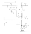
- FIG. 2 is a circuit diagram illustrating a detailed configuration example of a pixel or the like illustrated in FIG. 1.
- FIG. 3 is a cross-sectional view illustrating a configuration of a transistor illustrated in FIG. 2.
- 13 is a TEM (Transmission Electron Microscope) photograph (corresponding to the structure shown in FIG. 12) for explaining the film thickness of a silicon oxide film. It is sectional drawing which represented a part of FIG. 5A typically.
- FIG. 5A typically.
- FIG. 2 is a block diagram illustrating a detailed configuration example of a column selection unit illustrated in FIG. 1. It is a characteristic view for demonstrating the influence on the current-voltage characteristic of the transistor by an X-ray. It is sectional drawing for demonstrating the manufacturing process including the formation process of a semiconductor layer. It is sectional drawing showing the process of following FIG. 7B. It is sectional drawing showing the process of following FIG. 7C. It is sectional drawing showing the process of following FIG. 7D. It is a characteristic view showing the relationship between the sum total of the film thickness of a silicon oxide film, and a threshold voltage shift. 10 is a cross-sectional view illustrating a configuration of a transistor according to Modification 1. FIG.
- FIG. 10 is a cross-sectional view illustrating a configuration of a transistor according to Modification 2.
- FIG. 10 is a cross-sectional view illustrating a configuration of a transistor according to Modification 3-1.
- FIG. 10 is a cross-sectional view illustrating a configuration of a transistor according to Modification 3-2.
- FIG. 10 is a cross-sectional view illustrating a configuration of a transistor according to Modification 3-2.
- FIG. 10 is a circuit diagram illustrating a configuration of a pixel and the like according to Modification 4.
- FIG. 10 is a circuit diagram illustrating a configuration of a pixel and the like according to Modification 5.
- FIG. 16 is a circuit diagram illustrating a configuration of a pixel and the like according to modification 6-1.
- FIG. 16 is a circuit diagram illustrating a configuration of a pixel and the like according to modification example 6-2. It is a schematic diagram showing schematic structure of the imaging display system which concerns on an application example.
- Embodiment an example of a radiation imaging apparatus including a top-gate TFT in which the thickness of a silicon oxide film adjacent to the upper side of the semiconductor layer is larger than that of the silicon oxide film adjacent to the lower side
- Modification 1 (Another example of a top gate transistor) 3.
- Modification 2 (example of bottom gate transistor) 4).
- Modification 3-1 (Example of Dual Gate Transistor) 5.
- Modification 3-2 (Another example of dual gate transistor) 6).
- Modified example 4 an example of another passive pixel circuit) 7).
- Modified example 5 an example of another passive pixel circuit
- Modified examples 6-1 and 6-2 (example of active pixel circuit) 9.
- Application example (example of radiation imaging display system)
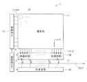
- FIG. 1 illustrates an overall block configuration of a radiation imaging apparatus (radiation imaging apparatus 1) according to an embodiment of the present disclosure.
- the radiation imaging apparatus 1 reads information on a subject (captures a subject) based on, for example, incident radiation Rrad (for example, ⁇ rays, ⁇ rays, ⁇ rays, X rays, etc.).
- the radiation imaging apparatus 1 includes a pixel unit 11, and includes a row scanning unit 13, an A / D conversion unit 14, a column scanning unit 15, and a system control unit 16 as a drive circuit for the pixel unit 11.
- the pixel unit 11 includes a plurality of pixels (imaging pixels, unit pixels) 20 that generate signal charges based on radiation.
- the plurality of pixels 20 are two-dimensionally arranged in a matrix (matrix).
- the horizontal direction (row direction) in the pixel unit 11 will be described as “H” direction and the vertical direction (column direction) will be described as “V” direction.
- the radiation imaging apparatus 1 may be either a so-called indirect conversion type or a direct conversion type as long as it uses a transistor 22 described later as a switching element for reading signal charges from the pixel unit 11.
- 2A shows the configuration of the pixel unit 11 in the case of the indirect conversion type
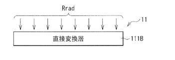
- FIG. 2B shows the configuration of the pixel unit 11 in the case of the direct conversion type.
- the pixel unit 11 has a wavelength conversion layer 112 on the photoelectric conversion layer 111A (light receiving surface side).
- the wavelength conversion layer 112 converts the radiation Rrad into a wavelength in the sensitivity range of the photoelectric conversion layer 111 (for example, visible light).
- This wavelength conversion layer 112 is, for example, a phosphor that converts X-rays into visible light (for example, CsI (added with Tl), Gd 2 O 2 S, BaFX (X is Cl, Br, I, etc.), NaI, CaF 2, etc. Scintillator).
- Such a wavelength conversion layer 112 is formed on the photoelectric conversion layer 111A through a planarization film made of, for example, an organic material or a spin-on-glass material.
- the photoelectric conversion layer 111A includes a photoelectric conversion element (a photoelectric conversion element 21 described later) such as a photodiode.
- the pixel unit 11 has a conversion layer (direct conversion layer 111B) that absorbs incident radiation Rrad and generates an electrical signal (holes and electrons).
- the direct conversion layer 111B is made of, for example, an amorphous selenium (a-Se) semiconductor, a cadmium tellurium (CdTe) semiconductor, or the like.
- the radiation imaging apparatus 1 may be either an indirect conversion type or a direct conversion type.
- the case of the indirect conversion type will be mainly described as an example. . That is, in the pixel unit 11, the radiation Rrad is converted into visible light in the wavelength conversion layer 112, and then the visible light is converted into an electric signal in the photoelectric conversion layer 111A (photoelectric conversion element 21). It is read out as a signal charge.
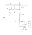
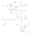
- FIG. 3 illustrates a circuit configuration of the pixel 20 (a so-called passive circuit configuration) together with a circuit configuration of a later-described charge amplifier circuit 171 in the A / D conversion unit 14.
- This passive pixel 20 is provided with one photoelectric conversion element 21 and one transistor 22.
- the pixel 20 is also connected to a read control line Lread extending along the H direction and a signal line Lsig extending along the V direction.
- the photoelectric conversion element 21 includes, for example, a PIN (Positive Intrinsic Negative) type photodiode or a MIS (Metal-Insulator-Semiconductor) type sensor, and generates a signal charge having a charge amount corresponding to the amount of incident light as described above.
- the cathode of the photoelectric conversion element 21 is connected to the storage node N here.
- the transistor 22 is turned on in response to the row scanning signal supplied from the read control line Lread, so that the signal charge (input voltage Vin) obtained by the photoelectric conversion element 21 is output to the signal line Lsig (read).
- Transistor is configured by an N channel type (N type) field effect transistor (FET).
- FET field effect transistor
- the transistor 22 may be composed of a P-channel type (P-type) FET or the like.
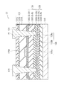
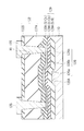
- FIG. 4 shows a cross-sectional structure of the transistor 22.
- the transistor 22 has a so-called top gate type thin film transistor element structure.
- the transistor 22 includes, for example, a first gate insulating film 129 (first gate insulating film), a semiconductor layer 126, a second gate insulating film 130 (second gate insulating film), and a first gate electrode 120A on a substrate 110. In this order.
- An interlayer insulating film 131 is formed on the first gate electrode 120A, and a contact hole H1 penetrating the interlayer insulating film 131 and the second gate insulating film 130 is formed.
- source / drain electrodes 128 are provided so as to fill the contact holes H1.
- the semiconductor layer 126 includes, for example, a channel layer (active layer) 126a, an LDD (Lightly Doped Drain) layer 126b, and an N + layer 126c.
- amorphous silicon amorphous silicon
- microcrystalline silicon or polycrystalline silicon (polysilicon)
- polysilicon polycrystalline silicon
- LTPS Low Temperature Poly-silicon
- oxide semiconductors such as indium gallium zinc oxide (InGaZnO) or zinc oxide (ZnO).
- the LDD layer 126b is formed between the channel layer 126a and the N + layer 126c for the purpose of reducing leakage current.
- the source / drain electrode 128 functions as a source or drain, and is a single-layer film made of any of titanium (Ti), aluminum (Al), molybdenum (Mo), tungsten (W), chromium (Cr), and the like. Or a laminated film containing two or more of them.
- the first gate electrode 120A is, for example, a single layer film made of any one of molybdenum, titanium, aluminum, tungsten, chromium, or the like, or a laminated film including two or more of them.
- the first gate electrode 120A is provided to face the semiconductor layer 126 (specifically, the channel layer 126a) with the second gate insulating film 130 in between (the semiconductor layer 126 faces the first gate electrode 120A). A region to be the channel layer 126a).
- Each of the first gate insulating film 129 and the second gate insulating film 130 includes a silicon oxide film (a silicon compound film containing oxygen) such as silicon oxide (SiO x ) or silicon oxynitride (SiON). Yes.
- the first gate insulating film 129 and the second gate insulating film 130 are each a single-layer film made of, for example, silicon oxide or silicon oxynitride, or such a silicon oxide film and silicon nitride A laminated film including a silicon nitride film such as a (SiN x ) film.
- the silicon oxide film is provided on the semiconductor layer 126 side (adjacent to the semiconductor layer 126).
- the semiconductor layer 126 is made of, for example, low-temperature polycrystalline silicon, a silicon oxide film is formed adjacent to the semiconductor layer 126 for reasons of the manufacturing process.
- the first gate insulating film 129 and the second gate insulating film 130 are each preferably a laminated film including the silicon oxide film and the silicon nitride film.
- the first gate insulating film 129 and the second gate insulating film 130 are each a laminated film.
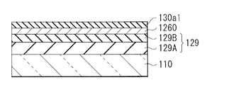
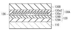
- the first gate insulating film 129 is formed by laminating, for example, a silicon nitride film 129A and a silicon oxide film 129B sequentially from the substrate 110 side.
- the second gate insulating film 130 is formed by stacking, for example, a silicon oxide film 130A, a silicon nitride film 130B, and a silicon oxide film 130C in this order from the semiconductor layer 126 side.
- the silicon oxide film 129B of this embodiment corresponds to a specific example of the “first silicon oxide film” of the present disclosure
- the silicon oxide film 130A corresponds to the “second silicon oxide film” of the present disclosure. This corresponds to a specific example.
- the thickness of the silicon oxide film 130A of the second gate insulating film 130 adjacent to the upper side (upper surface) of the semiconductor layer 126 is equal to the first gate insulating film 129 adjacent to the lower side (lower surface) of the semiconductor layer 126. This is equal to or higher than that of the silicon oxide film 129B. Further, the total thickness of the silicon oxide film 129B and the silicon oxide film 130A is desirably, for example, 65 nm or less. This is because the shift of the threshold voltage of the transistor 22 to the negative side can be reduced to suppress the characteristic deterioration.
- each thickness of the first gate insulating film 129 and the second gate insulating film 130 is, for example, in the first gate insulating film 129, the thickness of the silicon nitride film 129A is, for example, 30 nm to 120 nm, and the silicon oxide film The thickness of 129B is, for example, 5 nm to 60 nm.
- the thickness of the silicon oxide film 130A is, for example, 5 nm to 60 nm
- the thickness of the silicon nitride film 130B is, for example, 10 nm to 120 nm
- the thickness of the silicon oxide film 130C is, for example, 5 nm to 60 nm.
- the thicknesses of the silicon oxide films 129B and 130A are set so as to satisfy the above magnitude relationship, and preferably the total thickness is set to 65 nm or less.
- the capacitance (gate capacitance) between the semiconductor layer 126 and the first gate electrode 120A is determined according to the dielectric constant, thickness, and the like of each film constituting the second gate insulating film 130.
- the silicon oxide films 129B and 130A are adjacent to the semiconductor layer 126 for reasons of the manufacturing process. From the viewpoint of transistor characteristics (details will be described later), the silicon oxide films 129B and 130A It is desirable that the total thickness is relatively thin (for example, 65 nm or less). Therefore, in the second gate insulating film 130, the gate capacitance can be set by mainly adjusting the thickness of the silicon nitride film 130B in the stacked structure.
- the thickness of the silicon nitride film 130B is desirably larger than the thickness of the silicon oxide film 130A, for example, 10 nm or more. This makes it easier to form a desired gate capacitance while maintaining the total thickness of the silicon oxide film 129A and the silicon oxide film 130B at, for example, 65 nm or less.
- each film (particularly the silicon oxide film 130A) in the second gate insulating film 130 is desirably measured at a specific site as follows, for example. That is, as shown in FIG. 5A, in the stacked structure of the transistor 22, a minute protrusion X is likely to be generated on the surface of the semiconductor layer 126 (channel layer 126a) made of, for example, polycrystalline silicon. As a result, in each film above the semiconductor layer 126, particularly the silicon oxide film 130A, it is difficult to obtain good coverage in the vicinity of the protrusion X (it is likely to become thin locally). Therefore, as schematically shown in FIG. 5B, it is desirable to use the thickness (t) in the flat portion A between the protrusions X as the thickness of at least the silicon oxide film 130A of the second gate insulating film 130.
- the interlayer insulating film 131 is, for example, a single layer film made of any one of silicon oxide, silicon oxynitride, and silicon nitride, or a laminated film including two or more of them.
- the interlayer insulating film 131 is formed by laminating a silicon oxide film 131A, a silicon nitride film 131B, and a silicon oxide film 131C in this order from the first gate electrode 120A side.
- another interlayer insulating film may be formed so as to cover the interlayer insulating film 131 and the source / drain electrode 128.
- the row scanning unit 13 includes a shift register circuit, a predetermined logic circuit, and the like, which will be described later, and drives (line-sequentially) a plurality of pixels 20 in the pixel unit 11 in units of rows (horizontal line units).
- This is a pixel driver (row scanning circuit) that performs scanning. Specifically, an imaging operation such as a read operation or a reset operation of each pixel 20 is performed by, for example, line sequential scanning. Note that this line sequential scanning is performed by supplying the above-described row scanning signal to each pixel 20 via the readout control line Lread.
- the A / D conversion unit 14 has a plurality of column selection units 17 provided for each of a plurality (here, four) of signal lines Lsig, and the signal voltage (via the signal line Lsig ( A / D conversion (analog / digital conversion) is performed based on the voltage according to the signal charge. Thereby, output data Dout (imaging signal) composed of a digital signal is generated and output to the outside.
- each column selection unit 17 includes a charge amplifier 172, a capacitive element (capacitor or feedback capacitive element) C1, a switch SW1, a sample hold (S / H) circuit 173, and four switches SW2.
- a multiplexer circuit (selection circuit) 174 including the A / D converter 175 is included.
- the charge amplifier 172, the capacitor C1, the switch SW1, the S / H circuit 173, and the switch SW2 are provided for each signal line Lsig.
- the multiplexer circuit 174 and the A / D converter 175 are provided for each column selection unit 17.
- the charge amplifier 172, the capacitive element C1, and the switch SW1 constitute the charge amplifier circuit 171 shown in FIG.
- the charge amplifier 172 is an amplifier (amplifier) for converting the signal charge read from the signal line Lsig into a voltage (QV conversion).
- one end of the signal line Lsig is connected to the negative ( ⁇ ) input terminal, and a predetermined reset voltage Vrst is input to the positive (+) input terminal.
- the output terminal of the charge amplifier 172 and the negative input terminal are connected in a feedback manner (feedback connection) via a parallel connection circuit of the capacitive element C1 and the switch SW1. That is, one terminal of the capacitive element C1 is connected to the negative input terminal of the charge amplifier 172, and the other terminal is connected to the output terminal of the charge amplifier 172.
- one terminal of the switch SW1 is connected to the negative input terminal of the charge amplifier 172, and the other terminal is connected to the output terminal of the charge amplifier 172.
- the on / off state of the switch SW1 is controlled by a control signal (amplifier reset control signal) supplied from the system control unit 16 via the amplifier reset control line Lcarst.
- the S / H circuit 173 is disposed between the charge amplifier 172 and the multiplexer circuit 174 (switch SW2), and is a circuit for temporarily holding the output voltage Vca from the charge amplifier 172.
- the multiplexer circuit 174 selectively connects each S / H circuit 173 and the A / D converter 175 by sequentially turning on one of the four switches SW2 in accordance with the scanning drive by the column scanning unit 15. Or it is a circuit to cut off.
- the A / D converter 175 is a circuit that generates and outputs the output data Dout by performing A / D conversion on the output voltage from the S / H circuit 173 input through the switch SW2. .
- the column scanning unit 15 includes, for example, a shift register and an address decoder (not shown), and drives the switches SW2 in the column selection unit 17 in order while scanning.
- the signal (the output data Dout) of each pixel 20 read through each of the signal lines Lsig is sequentially output to the outside.
- the system control unit 16 controls the operations of the row scanning unit 13, the A / D conversion unit 14, and the column scanning unit 15. Specifically, the system control unit 16 includes a timing generator that generates the various timing signals (control signals) described above, and the row scanning unit based on the various timing signals generated by the timing generator. 13. Drive control of the A / D conversion unit 14 and the column scanning unit 15 is performed. Based on the control of the system control unit 16, the row scanning unit 13, the A / D conversion unit 14, and the column scanning unit 15 perform imaging driving (line sequential imaging driving) for each of the plurality of pixels 20 in the pixel unit 11. Thus, the output data Dout is acquired from the pixel unit 11.
- imaging driving line sequential imaging driving
- the signal charges read in this way are input to the column selection unit 17 in the A / D conversion unit 14 for each of a plurality (here, four) of pixel columns via the signal line Lsig.
- the column selection unit 17 first performs QV conversion (conversion from signal charge to signal voltage) in a charge amplifier circuit including a charge amplifier 172 and the like for each signal charge input from each signal line Lsig.
- QV conversion conversion from signal charge to signal voltage
- a / D conversion is performed in the A / D converter 175 via the S / H circuit 173 and the multiplexer circuit 174 for each converted signal voltage (output voltage Vca from the charge amplifier 172), and an output consisting of a digital signal is performed.
- Data Dout imaging signal
- the output data Dout is sequentially output from each column selection unit 17 and transmitted to the outside (or input to an internal memory not shown).
- the transistor 22 includes silicon oxide films (silicon oxide films 129B and 130A) in the first gate insulating film 129 and the second gate insulating film 130.
- silicon oxide films silicon oxide films 129B and 130A
- electrons in the films are excited by the so-called photoelectric effect, Compton scattering, or electron pair generation.
- the threshold voltage Vth of the transistor 22 is shifted to the negative side (minus side), the S (threshold) value is deteriorated, and the like, which causes an increase in off current or a decrease in on current.
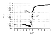
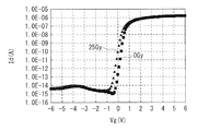
- FIG. 7A shows the relationship (current-voltage characteristics) of the drain current (current between the source and drain) Id with respect to the gate voltage Vg of the transistor 22 for each X-ray irradiation dose.
- Irradiation conditions are a tube voltage of 80 kV, a dose rate of 3.2 mGy / sec, and the irradiation dose is 0 Gy (initial value), 54 Gy, 79 Gy, 104 Gy, 129 Gy, 154 Gy, 254 Gy, and 354 Gy.
- low-temperature polycrystalline silicon is used for the semiconductor layer 126, and the voltage Vds between the source and the drain is 0.1V.
- the surface of the semiconductor layer 126 is likely to be rough (protrusions X are easily generated), and the silicon oxide film 130A is likely to be locally thin.
- the thickness of the silicon oxide film 130A of the second gate insulating film 130 is equal to or greater than the thickness of the silicon oxide film 129B of the first gate insulating film 129. Coverage is obtained, and transistor characteristics (threshold voltage characteristics or S value) are improved. In addition, variations in the characteristics of each element can be suppressed.
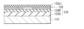
- stopper film 130a1 made of, for example, silicon oxide (SiO 2 ) is used.
- SiO 2 silicon oxide
- the stopper film 130a1 is formed on the polysilicon layer 1260. To do. Subsequently, as shown in FIG. 7C, the polysilicon layer 1260 is doped with impurities through the stopper film 130a1 to form the semiconductor layer 126. In this manner, by using the stopper film 130a1 when the semiconductor layer 126 is formed, the process can be performed without exposing (not exposing) the interface of the semiconductor layer 126 (particularly, the channel layer 126a).
- the semiconductor layer 126 and the stopper film 130a1 are patterned into a predetermined shape.
- the end face of the semiconductor layer 126 (side face of the N + layer 126c) is exposed.
- the silicon nitride film 130B is formed in this state, the threshold voltage shifts to the negative side due to the influence of the interface state. It becomes easy to do. Therefore, as shown in FIG. 7E, another layer of silicon oxide film 130a2 is formed so as to cover the end face of the semiconductor layer 126 and the stopper film 130a1.
- deterioration of the transistor characteristics can be suppressed when the thickness of the upper silicon oxide film 130A is equal to or greater than the thickness of the lower silicon oxide film 129B of the semiconductor layer 126.
- the characteristics of the transistor 22 are improved. This is particularly effective when the total thickness of the silicon oxide films 129B and 130A adjacent to the semiconductor layer 126 is set to 65 nm or less (thinned) as will be described later.
- the characteristic deterioration due to the hole trap as described above can also be suppressed, and the reliability can be further improved.
- FIG. 7F shows the relationship between the total thickness (total thickness) of the silicon oxide (SiO 2 ) film and the threshold voltage shift amount ( ⁇ Vth).
- the sign of ⁇ (minus) on the vertical axis indicates that the threshold voltage is shifted to the negative side.
- the thickness of the silicon oxide film and the threshold voltage there is a correlation between the thickness of the silicon oxide film and the threshold voltage, and it has linearity. For example, when the total thickness of the silicon oxide films 129B and 130A is 65 nm or less, the shift amount can be maintained at 2 V or less, and a sufficient transistor life can be ensured.
- the transistor 22 for reading out signal charges based on the radiation Rrad from each pixel 20 includes the silicon oxide film 129B, the semiconductor layer 126, the silicon oxide film 130A, and the first electrode in order from the substrate 110 side. And an element structure including a gate electrode. Since the thickness of the silicon oxide film 130A is equal to or greater than the thickness of the silicon oxide film 129B, the manufacturing yield of the transistor 22 is improved. Therefore, a highly reliable element structure can be realized.
- FIG. 8 illustrates a cross-sectional configuration of a transistor according to the first modification.
- the second gate insulating film (second gate insulating film 130) is formed by sequentially forming the silicon oxide film 130A, the silicon nitride film 130B, and the silicon oxide film 130C from the semiconductor layer 126 side.
- the stacked three-layer structure is used, the stacked structure of the second gate insulating film is not limited to this.
- a two-layer structure in which a silicon oxide film 134A and a silicon nitride film 134B are stacked in this order from the semiconductor layer 126 side as in the second gate insulating film (second gate insulating film 134). May be.
- FIG. 9A shows current-voltage characteristics before and after X-ray irradiation of the transistor 22 (referred to as Example 1) in the above embodiment
- FIG. 9B shows before and after X-ray irradiation of the transistor according to this modification (referred to as Example 2). It represents current-voltage characteristics.
- the X-ray irradiation conditions are the same as those in the case of FIG.
- FIG. 10 shows the threshold voltage shift amount ( ⁇ Vth) after X-ray irradiation (25 Gy) in the current-voltage characteristics of Examples 1 and 2.
- the threshold voltage Vth the gate voltage in the case where the current Id is 1.0 ⁇ 10 ⁇ 13 (A) is used.
- the current-voltage characteristics in the element structure of this modification are the same as those in the above embodiment, and the behavior by X-ray irradiation is also the same. Therefore, also in this modification, the same effect as the above-described embodiment can be obtained.
- the second gate insulating film 130 may have a three-layer structure. It may be a layered structure.
- the second gate insulating film 130 may be composed of, for example, a single layer film of a silicon oxide film 130A.
- FIG. 11 illustrates a cross-sectional configuration of a transistor according to the second modification.
- a top-gate element structure is illustrated, but the transistor of the present disclosure may have a so-called bottom-gate element structure as in the present modification.
- the element structure of this modification includes, for example, a first gate electrode 120A, a first gate insulating film 129, a semiconductor layer 126, and a silicon oxide film 130A in order from the substrate 110 side.
- an interlayer insulating film 132 is formed on the silicon oxide film 130A, and a contact hole H1 penetrating the interlayer insulating film 132 and the silicon oxide film 130A is formed.
- the interlayer insulating film 132 is a stacked film including, for example, a silicon nitride film 132A and a silicon oxide film 132B in this order from the silicon oxide film 130A side.
- the thickness of the silicon oxide film 130A is equal to or greater than the thickness of the silicon oxide film 129B, an effect equivalent to that of the above embodiment can be obtained.
- the thickness of the silicon nitride film 132A of the interlayer insulating film 132 is desirably larger than the thickness of the silicon oxide film 130A (for example, 10 nm or more).
- the total thickness of the silicon oxide films 129B and 130a adjacent to the semiconductor layer 126 is desirably 65 nm or less.
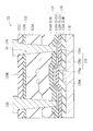
- FIG. 12 illustrates a cross-sectional configuration of a transistor according to Modification 3-1.
- the top gate type element structure is illustrated, but the transistor of the present disclosure may have a so-called dual gate type element structure as in the present modification.
- the element structure of this modification has, for example, a first gate electrode 120A, a first gate insulating film 129, a semiconductor layer 126, a second gate insulating film 130, and a second gate electrode 120B in this order from the substrate 110 side.
- An interlayer insulating film 133 is formed on the second gate insulating film 130 and the second gate electrode 120B, and a contact hole H1 penetrating the interlayer insulating film 133 and the second gate insulating film 130 is formed. ing. On the interlayer insulating film 133, source / drain electrodes 128 are provided so as to fill the contact holes H1.
- the interlayer insulating film 133 is a stacked film including, for example, a silicon oxide film 133A, a silicon nitride film 133B, and a silicon oxide film 133C in this order from the silicon oxide film 130A side.
- the thickness of the silicon oxide film 130A is equal to or greater than the thickness of the silicon oxide film 129B, an effect equivalent to that of the above embodiment can be obtained.
- the thickness of the silicon nitride film 132A of the interlayer insulating film 132 is larger than the thickness of the silicon oxide film 130A (for example, 10 nm or more).
- the total thickness of the silicon oxide films 129B and 130a adjacent to the semiconductor layer 126 is desirably 65 nm or less.
- FIG. 13 illustrates a cross-sectional configuration of a transistor according to Modification 3-2.
- the laminated structure of the second gate insulating film is not particularly limited, and the second-layered second gate insulating film 134 described in the modified example 1 is used. May be.
- FIG. 14 illustrates a circuit configuration of a pixel (pixel 20A) according to Modification 4 together with the circuit configuration example of the charge amplifier circuit 171 described in the above embodiment.
- the pixel 20 ⁇ / b> A of this modification has a so-called passive circuit configuration, and includes one photoelectric conversion element 21 and one transistor 22.
- the pixel 20A is connected to a read control line Lread extending along the H direction and a signal line Lsig extending along the V direction.
- the anode of the photoelectric conversion element 21 is connected to the storage node N, and the cathode is connected to the ground (ground).
- the storage node N may be connected to the anode of the photoelectric conversion element 21 in the pixel 20A, and even in such a configuration, the same as the radiation imaging apparatus 1 of the above embodiment. An effect can be obtained.
- FIG. 15 illustrates a circuit configuration of a pixel (pixel 20B) according to Modification 5 together with the circuit configuration example of the charge amplifier circuit 171 described in the above embodiment.
- the pixel 20B according to the present modification has a so-called passive circuit configuration, includes one photoelectric conversion element 21, and a read control line Lread extending in the H direction. , And a signal line Lsig extending along the V direction.
- the pixel 20 ⁇ / b> B has two transistors 22. These two transistors 22 are connected to each other in series (one source or drain and the other source or drain are electrically connected. In this way, two transistors 22 are provided in one pixel 20B. Thus, off-leakage can be reduced.
- two transistors 22 connected in series may be provided in the pixel 20B, and in this case as well, the same effect as in the above embodiment can be obtained.
- Three or more transistors may be connected in series.
- FIG. 16 illustrates a circuit configuration of a pixel (pixel 20C) according to Modification 6-1 along with a circuit configuration example of a charge amplifier circuit 171A described below.
- FIG. 17 shows the circuit configuration of the pixel (pixel 20D) according to the modification 6-2 together with the circuit configuration example of the charge amplifier circuit 171A.
- the pixels 20 C and 20 D according to these modified examples 6-1 and 6-2 have so-called active pixel circuits.
- the active pixels 20C and 20D are provided with one photoelectric conversion element 21 and three transistors 22, 23, and 24.
- a read control line Lread and a reset control line Lrst extending along the H direction and a signal line Lsig extending along the V direction are also connected to the pixels 20C and 20D.
- the gate of the transistor 22 is connected to the read control line Lread, the source is connected to the signal line Lsig, and the drain is connected to the drain of the transistor 23 constituting the source follower circuit.
- the source of the transistor 23 is connected to the power supply VDD, the gate is connected to the cathode (example in FIG. 16) or the anode (example in FIG. 17) of the photoelectric conversion element 21 via the storage node N, and the transistor functions as a reset transistor. 24 drains.
- the gate of the transistor 24 is connected to the reset control line Lrst, and the reset voltage Vrst is applied to the source.
- the anode of the photoelectric conversion element 21 is connected to the ground
- Modification Example 6-2 the cathode of the photoelectric conversion element 21 is connected to the ground.
- the charge amplifier circuit 171A is provided with an amplifier 176 and a constant current source 177 instead of the charge amplifier 172, the capacitive element C1, and the switch SW1 in the charge amplifier circuit 171 described above. It is a thing.
- the signal line Lsig is connected to the positive input terminal, and the negative input terminal and the output terminal are connected to each other to form a voltage follower circuit.
- one terminal of the constant current source 177 is connected to one end side of the signal line Lsig, and the power source VSS is connected to the other terminal of the constant current source 177.
- the indirect conversion type or direct conversion type radiation imaging apparatus as described above is used as various types of radiation imaging apparatuses that obtain an electrical signal based on the radiation Rrad.
- medical X-ray imaging devices Digital Radiography, etc.
- X-ray imaging devices for portable object inspection used at airports, etc. X-ray imaging devices for portable object inspection used at airports, etc.
- industrial X-ray imaging devices for example, devices for inspecting dangerous goods in containers, etc.
- FIG. 18 schematically illustrates a schematic configuration example of a radiation imaging display system (radiation imaging display system 5) according to an application example.
- the radiation imaging display system 5 includes a radiation imaging apparatus 1 including the pixel unit 11 and the like according to the above-described embodiment, an image processing unit 52, and a display device 4, and in this example, radiation imaging using radiation It is a display system.
- the image processing unit 52 generates image data D1 by performing predetermined image processing on the output data Dout (imaging signal) output from the radiation imaging apparatus 1.
- the display device 4 performs image display on the predetermined monitor screen 40 based on the image data D ⁇ b> 1 generated by the image processing unit 52.
- the radiation imaging apparatus 1 acquires image data Dout of the subject 50 based on the radiation Rrad emitted toward the subject 50 from the radiation source 51 such as an X-ray source, and the image processing unit 52. Output to.
- the image processing unit 52 performs the predetermined image processing described above on the input image data Dout, and outputs the image data (display data) D1 after the image processing to the display device 4.
- the display device 4 displays image information (captured image) on the monitor screen 40 based on the input image data D1.
- the image of the subject 50 can be acquired as an electrical signal in the radiation imaging apparatus 1, image display is performed by transmitting the acquired electrical signal to the display device 4. It can be carried out. That is, it is possible to observe the image of the subject 50 without using a photographic film, and it is also possible to handle moving image shooting and moving image display.
- the first and second gate insulating films are illustrated by laminating one to three insulating films, but the first and second gate insulating films include four or more insulating films. It may be a laminate of films. In any stacked structure, a silicon oxide film is provided on the semiconductor layer side of the second gate insulating film, and this silicon oxide film is equal to or greater than the thickness of the silicon oxide film in the first gate insulating film. If it is formed with the thickness, the effect of the present disclosure can be obtained.
- circuit configuration of the pixel in the pixel portion of the above-described embodiment and the like is not limited to that described in the above-described embodiment (circuit configuration of the pixels 20, 20A to 20D), and other circuit configurations may be used. Good.
- circuit configurations of the row scanning unit, the column selection unit, and the like are not limited to those described in the above embodiments and the like, and other circuit configurations may be used.
- the pixel unit, the row scanning unit, the A / D conversion unit (column selection unit), the column scanning unit, and the like described in the above embodiments may be formed on the same substrate, for example.
- a polycrystalline semiconductor such as low-temperature polycrystalline silicon
- switches and the like in these circuit portions can be formed on the same substrate. For this reason, for example, it becomes possible to perform a driving operation on the same substrate based on a control signal from an external system control unit, and to improve reliability when narrowing the frame (three-side free frame structure) or wiring connection. Can be realized.
- this indication can also take the following structures.
- a plurality of pixels generating signal charges based on radiation;
- a field effect transistor for reading out the signal charge from the plurality of pixels, The transistor is A first silicon oxide film, a semiconductor layer including an active layer, and a second silicon oxide film, which are sequentially stacked from the substrate side;
- a first gate electrode disposed opposite to the semiconductor layer with the first or second silicon oxide film in between, The thickness of the second silicon oxide film is equal to or greater than the thickness of the first silicon oxide film.
- the radiation imaging apparatus according to (6) wherein a silicon nitride film having a thickness larger than that of the second silicon oxide film is provided on the second silicon oxide film.
- the thickness of the silicon nitride film is 10 nm or more.
- the transistor includes, in order from the substrate side, the first gate electrode, the first silicon oxide film, the semiconductor layer, and the second silicon oxide film, and the second silicon oxide film
- the radiation imaging apparatus according to (1) further including a second gate electrode facing the first gate electrode.
- the semiconductor layer includes low-temperature polycrystalline silicon.
- Each of the plurality of pixels has a photoelectric conversion element;
- the radiation imaging apparatus 15) The radiation imaging apparatus according to (14), wherein the photoelectric conversion element includes a PIN type photodiode or a MIS type sensor. (16) The radiation imaging apparatus according to any one of (1) to (13), wherein each of the plurality of pixels includes a conversion layer that absorbs the radiation and generates the signal charge. (17) The radiation imaging apparatus according to any one of (1) to (16), wherein the radiation is X-rays.
- the radiation imaging apparatus includes: A plurality of pixels generating signal charges based on radiation; A field effect transistor for reading out the signal charge from the plurality of pixels, The transistor is A first silicon oxide film, a semiconductor layer including an active layer, and a second silicon oxide film, which are sequentially stacked from the substrate side; A first gate electrode disposed opposite to the semiconductor layer with the first or second silicon oxide film in between, The radiation imaging display system, wherein the thickness of the second silicon oxide film is equal to or greater than the thickness of the first silicon oxide film.
Landscapes
- Engineering & Computer Science (AREA)
- Multimedia (AREA)
- Signal Processing (AREA)
- Solid State Image Pick-Up Elements (AREA)
- Thin Film Transistor (AREA)
- Health & Medical Sciences (AREA)
- Toxicology (AREA)
- Chemical & Material Sciences (AREA)
- Crystallography & Structural Chemistry (AREA)
- Microelectronics & Electronic Packaging (AREA)
- Transforming Light Signals Into Electric Signals (AREA)
Priority Applications (3)
| Application Number | Priority Date | Filing Date | Title |
|---|---|---|---|
| US14/905,041 US20160163762A1 (en) | 2013-07-17 | 2014-07-03 | Radiation image pickup unit and radiation image pickup display system |
| CN201480039175.1A CN105359272A (zh) | 2013-07-17 | 2014-07-03 | 放射线摄像装置和放射线摄像显示系统 |
| KR1020157037232A KR20160033668A (ko) | 2013-07-17 | 2014-07-03 | 방사선 촬상 장치 및 방사선 촬상 표시 시스템 |
Applications Claiming Priority (2)
| Application Number | Priority Date | Filing Date | Title |
|---|---|---|---|
| JP2013148271A JP2015023079A (ja) | 2013-07-17 | 2013-07-17 | 放射線撮像装置および放射線撮像表示システム |
| JP2013-148271 | 2013-07-17 |
Publications (1)
| Publication Number | Publication Date |
|---|---|
| WO2015008630A1 true WO2015008630A1 (ja) | 2015-01-22 |
Family
ID=52346099
Family Applications (1)
| Application Number | Title | Priority Date | Filing Date |
|---|---|---|---|
| PCT/JP2014/067752 Ceased WO2015008630A1 (ja) | 2013-07-17 | 2014-07-03 | 放射線撮像装置および放射線撮像表示システム |
Country Status (6)
| Country | Link |
|---|---|
| US (1) | US20160163762A1 (https=) |
| JP (1) | JP2015023079A (https=) |
| KR (1) | KR20160033668A (https=) |
| CN (1) | CN105359272A (https=) |
| TW (1) | TWI643323B (https=) |
| WO (1) | WO2015008630A1 (https=) |
Cited By (2)
| Publication number | Priority date | Publication date | Assignee | Title |
|---|---|---|---|---|
| JP2016146626A (ja) * | 2015-01-30 | 2016-08-12 | 株式会社半導体エネルギー研究所 | 撮像装置および電子機器 |
| JP7015959B1 (ja) | 2021-07-29 | 2022-02-03 | 株式会社堀場製作所 | 放射線検出素子の製造方法 |
Families Citing this family (5)
| Publication number | Priority date | Publication date | Assignee | Title |
|---|---|---|---|---|
| JP2017143135A (ja) * | 2016-02-09 | 2017-08-17 | 株式会社ジャパンディスプレイ | 薄膜トランジスタ |
| JP2017162852A (ja) * | 2016-03-07 | 2017-09-14 | 株式会社ジャパンディスプレイ | 半導体装置および表示装置 |
| CN109276268A (zh) * | 2018-11-21 | 2019-01-29 | 京东方科技集团股份有限公司 | X射线探测装置及其制造方法 |
| US12150319B2 (en) | 2019-02-08 | 2024-11-19 | Georgia Tech Research Corporation | High sensitivity stable sensors and methods for manufacturing same |
| JP2020129635A (ja) * | 2019-02-12 | 2020-08-27 | 株式会社ジャパンディスプレイ | 半導体装置および半導体装置の製造方法 |
Citations (3)
| Publication number | Priority date | Publication date | Assignee | Title |
|---|---|---|---|---|
| JP2011176235A (ja) * | 2010-02-25 | 2011-09-08 | Sony Corp | 放射線撮像装置およびその駆動方法 |
| JP2012028617A (ja) * | 2010-07-26 | 2012-02-09 | Sony Corp | 放射線検出装置及び放射線撮像装置 |
| JP2012146805A (ja) * | 2011-01-12 | 2012-08-02 | Sony Corp | 放射線撮像装置、放射線撮像表示システムおよびトランジスタ |
Family Cites Families (7)
| Publication number | Priority date | Publication date | Assignee | Title |
|---|---|---|---|---|
| JP4266656B2 (ja) | 2003-02-14 | 2009-05-20 | キヤノン株式会社 | 固体撮像装置及び放射線撮像装置 |
| US20080042131A1 (en) * | 2006-08-15 | 2008-02-21 | Tpo Displays Corp. | System for displaying images including thin film transistor device and method for fabricating the same |
| JP4420032B2 (ja) * | 2007-01-31 | 2010-02-24 | ソニー株式会社 | 薄膜半導体装置の製造方法 |
| JP4355747B2 (ja) | 2007-03-05 | 2009-11-04 | キヤノン株式会社 | 光電変換装置及び光電変換システム並びにその駆動方法 |
| JP4524699B2 (ja) * | 2007-10-17 | 2010-08-18 | ソニー株式会社 | 表示装置 |
| JP5392545B2 (ja) * | 2009-03-13 | 2014-01-22 | ソニー株式会社 | 表示装置 |
| JP5796760B2 (ja) * | 2009-07-29 | 2015-10-21 | Nltテクノロジー株式会社 | トランジスタ回路 |
-
2013
- 2013-07-17 JP JP2013148271A patent/JP2015023079A/ja active Pending
-
2014
- 2014-06-12 TW TW103120375A patent/TWI643323B/zh not_active IP Right Cessation
- 2014-07-03 WO PCT/JP2014/067752 patent/WO2015008630A1/ja not_active Ceased
- 2014-07-03 US US14/905,041 patent/US20160163762A1/en not_active Abandoned
- 2014-07-03 KR KR1020157037232A patent/KR20160033668A/ko not_active Abandoned
- 2014-07-03 CN CN201480039175.1A patent/CN105359272A/zh active Pending
Patent Citations (3)
| Publication number | Priority date | Publication date | Assignee | Title |
|---|---|---|---|---|
| JP2011176235A (ja) * | 2010-02-25 | 2011-09-08 | Sony Corp | 放射線撮像装置およびその駆動方法 |
| JP2012028617A (ja) * | 2010-07-26 | 2012-02-09 | Sony Corp | 放射線検出装置及び放射線撮像装置 |
| JP2012146805A (ja) * | 2011-01-12 | 2012-08-02 | Sony Corp | 放射線撮像装置、放射線撮像表示システムおよびトランジスタ |
Cited By (5)
| Publication number | Priority date | Publication date | Assignee | Title |
|---|---|---|---|---|
| JP2016146626A (ja) * | 2015-01-30 | 2016-08-12 | 株式会社半導体エネルギー研究所 | 撮像装置および電子機器 |
| US11848341B2 (en) | 2015-01-30 | 2023-12-19 | Semiconductor Energy Laboratory Co., Ltd. | Imaging device and electronic device |
| US12243885B2 (en) | 2015-01-30 | 2025-03-04 | Semiconductor Energy Laboratory Co., Ltd. | Imaging device and electronic device |
| JP7015959B1 (ja) | 2021-07-29 | 2022-02-03 | 株式会社堀場製作所 | 放射線検出素子の製造方法 |
| JP2023019637A (ja) * | 2021-07-29 | 2023-02-09 | 株式会社堀場製作所 | 放射線検出素子の製造方法 |
Also Published As
| Publication number | Publication date |
|---|---|
| TWI643323B (zh) | 2018-12-01 |
| TW201505166A (zh) | 2015-02-01 |
| US20160163762A1 (en) | 2016-06-09 |
| CN105359272A (zh) | 2016-02-24 |
| KR20160033668A (ko) | 2016-03-28 |
| JP2015023079A (ja) | 2015-02-02 |
Similar Documents
| Publication | Publication Date | Title |
|---|---|---|
| CN102593164B (zh) | 放射线摄像装置、放射线摄像显示系统以及晶体管 | |
| JP6152729B2 (ja) | 撮像装置および撮像表示システム | |
| JP5978625B2 (ja) | 放射線撮像装置、放射線撮像表示システムおよびトランジスタ | |
| US9859315B2 (en) | Radiation image-pickup device and radiation image-pickup display system | |
| CN103456753B (zh) | 摄像装置和摄像显示系统 | |
| JP5874670B2 (ja) | 撮像装置および撮像表示システム | |
| WO2015008630A1 (ja) | 放射線撮像装置および放射線撮像表示システム | |
| US20140291670A1 (en) | Image pickup device and image pickup display system | |
| JP6190192B2 (ja) | 放射線撮像装置および放射線撮像表示システム | |
| JP6166128B2 (ja) | 放射線撮像装置および放射線撮像表示システム |
Legal Events
| Date | Code | Title | Description |
|---|---|---|---|
| WWE | Wipo information: entry into national phase |
Ref document number: 201480039175.1 Country of ref document: CN |
|
| 121 | Ep: the epo has been informed by wipo that ep was designated in this application |
Ref document number: 14826427 Country of ref document: EP Kind code of ref document: A1 |
|
| ENP | Entry into the national phase |
Ref document number: 20157037232 Country of ref document: KR Kind code of ref document: A |
|
| WWE | Wipo information: entry into national phase |
Ref document number: 14905041 Country of ref document: US |
|
| NENP | Non-entry into the national phase |
Ref country code: DE |
|
| 122 | Ep: pct application non-entry in european phase |
Ref document number: 14826427 Country of ref document: EP Kind code of ref document: A1 |