WO2014204209A1 - 수직형 채널을 구비하는 질화물계 트랜지스터 및 이의 제조 방법 - Google Patents
수직형 채널을 구비하는 질화물계 트랜지스터 및 이의 제조 방법 Download PDFInfo
- Publication number
- WO2014204209A1 WO2014204209A1 PCT/KR2014/005371 KR2014005371W WO2014204209A1 WO 2014204209 A1 WO2014204209 A1 WO 2014204209A1 KR 2014005371 W KR2014005371 W KR 2014005371W WO 2014204209 A1 WO2014204209 A1 WO 2014204209A1
- Authority
- WO
- WIPO (PCT)
- Prior art keywords
- semiconductor layer
- nitride
- trench
- layer
- vertical channel
- Prior art date
- Legal status (The legal status is an assumption and is not a legal conclusion. Google has not performed a legal analysis and makes no representation as to the accuracy of the status listed.)
- Ceased
Links
Images





Classifications
-
- H—ELECTRICITY
- H10—SEMICONDUCTOR DEVICES; ELECTRIC SOLID-STATE DEVICES NOT OTHERWISE PROVIDED FOR
- H10P—GENERIC PROCESSES OR APPARATUS FOR THE MANUFACTURE OR TREATMENT OF DEVICES COVERED BY CLASS H10
- H10P10/00—Bonding of wafers, substrates or parts of devices
-
- H—ELECTRICITY
- H10—SEMICONDUCTOR DEVICES; ELECTRIC SOLID-STATE DEVICES NOT OTHERWISE PROVIDED FOR
- H10D—INORGANIC ELECTRIC SEMICONDUCTOR DEVICES
- H10D30/00—Field-effect transistors [FET]
- H10D30/01—Manufacture or treatment
- H10D30/015—Manufacture or treatment of FETs having heterojunction interface channels or heterojunction gate electrodes, e.g. HEMT
-
- H—ELECTRICITY
- H10—SEMICONDUCTOR DEVICES; ELECTRIC SOLID-STATE DEVICES NOT OTHERWISE PROVIDED FOR
- H10D—INORGANIC ELECTRIC SEMICONDUCTOR DEVICES
- H10D30/00—Field-effect transistors [FET]
- H10D30/40—FETs having zero-dimensional [0D], one-dimensional [1D] or two-dimensional [2D] charge carrier gas channels
- H10D30/47—FETs having zero-dimensional [0D], one-dimensional [1D] or two-dimensional [2D] charge carrier gas channels having two-dimensional [2D] charge carrier gas channels, e.g. nanoribbon FETs or high electron mobility transistors [HEMT]
- H10D30/471—High electron mobility transistors [HEMT] or high hole mobility transistors [HHMT]
- H10D30/476—High electron mobility transistors [HEMT] or high hole mobility transistors [HHMT] having gate trenches interrupting the 2D charge carrier gas channels, e.g. hybrid MOS-HEMTs
-
- H—ELECTRICITY
- H10—SEMICONDUCTOR DEVICES; ELECTRIC SOLID-STATE DEVICES NOT OTHERWISE PROVIDED FOR
- H10D—INORGANIC ELECTRIC SEMICONDUCTOR DEVICES
- H10D30/00—Field-effect transistors [FET]
- H10D30/40—FETs having zero-dimensional [0D], one-dimensional [1D] or two-dimensional [2D] charge carrier gas channels
- H10D30/47—FETs having zero-dimensional [0D], one-dimensional [1D] or two-dimensional [2D] charge carrier gas channels having two-dimensional [2D] charge carrier gas channels, e.g. nanoribbon FETs or high electron mobility transistors [HEMT]
- H10D30/471—High electron mobility transistors [HEMT] or high hole mobility transistors [HHMT]
- H10D30/477—Vertical HEMTs or vertical HHMTs
-
- H—ELECTRICITY
- H10—SEMICONDUCTOR DEVICES; ELECTRIC SOLID-STATE DEVICES NOT OTHERWISE PROVIDED FOR
- H10D—INORGANIC ELECTRIC SEMICONDUCTOR DEVICES
- H10D62/00—Semiconductor bodies, or regions thereof, of devices having potential barriers
- H10D62/80—Semiconductor bodies, or regions thereof, of devices having potential barriers characterised by the materials
- H10D62/85—Semiconductor bodies, or regions thereof, of devices having potential barriers characterised by the materials being Group III-V materials, e.g. GaAs
- H10D62/8503—Nitride Group III-V materials, e.g. AlN or GaN
-
- H—ELECTRICITY
- H10—SEMICONDUCTOR DEVICES; ELECTRIC SOLID-STATE DEVICES NOT OTHERWISE PROVIDED FOR
- H10D—INORGANIC ELECTRIC SEMICONDUCTOR DEVICES
- H10D64/00—Electrodes of devices having potential barriers
- H10D64/20—Electrodes characterised by their shapes, relative sizes or dispositions
- H10D64/27—Electrodes not carrying the current to be rectified, amplified, oscillated or switched, e.g. gates
- H10D64/311—Gate electrodes for field-effect devices
- H10D64/411—Gate electrodes for field-effect devices for FETs
Definitions
- the present disclosure relates generally to nitride-based transistors, and more particularly, to nitride-based transistors having a vertical channel and a method of manufacturing the same.
- gallium nitride-based transistors which have recently emerged, are capable of high-speed switching operation compared to conventional silicon transistors, and are suitable for high-speed signal processing and have high merit for high-voltage environment due to the high voltage resistance of the material itself. have.
- HEMT High Electron Mobility Transistor
- 2DEG two-dimensional electron gas
- the nitride based transistor 100 includes an undoped GaN semiconductor layer 110, an AlGaN semiconductor layer 120, a source electrode 130, a drain electrode 140, and a gate electrode 150. can do.
- the 2DEG layer 125 is formed near the interface between the undoped GaN semiconductor layer 110 and the AlGaN semiconductor layer 120.
- the gate electrode 150 may control a current flow moving through the channel 125.
- the breakdown voltage is determined in proportion to the distance Lgd between the gate and the drain. Therefore, in order to increase the breakdown voltage, it is necessary to maintain the distance Lgd between the gate and the drain more than a predetermined distance. have. As a result, it may be difficult to reduce the chip size.
- nitride-based transistors each having a source electrode and a drain electrode disposed opposite the substrate have been proposed.
- US Patent Publication No. 2012-0319127 discloses a current aperture vertical electron transistor (CAVET) as one of the above-described nitride-based transistors.
- CAVET current aperture vertical electron transistor
- a P-type GaN layer is disposed between the source electrode and the drain electrode as a current barrier layer, and a current flows through an aperture between the P-type GaN layers.
- Embodiments of the present disclosure provide a nitride-based transistor having a vertical channel having high current capacity, low operating resistance, and high operating reliability.
- Embodiments of the present disclosure provide a method of manufacturing a nitride-based transistor having the vertical channel.
- the nitride-based transistor may include a first nitride-based first semiconductor layer doped with a first type, a first nitride-based second semiconductor layer doped with a second type disposed on the first semiconductor layer, and the second semiconductor layer.
- a third nitride doped first semiconductor layer disposed in the first type, disposed along an inner wall of the trench formed to penetrate at least the second semiconductor layer and the third semiconductor layer, and the third semiconductor outside the trench;
- a second nitride-based fourth semiconductor layer disposed on the layer, and a gate electrode formed on the fourth semiconductor layer.
- the second nitride-based fourth semiconductor layer includes a nitride having an energy band gap different from that of the first nitride-based first to third semiconductor layers.
- a method of manufacturing a nitride-based transistor having a vertical channel is provided.
- first, a first nitride-based first semiconductor layer doped with a first type, a first nitride-based second semiconductor layer doped with a second type, and a first type doped on a substrate The first nitride-based third semiconductor layer is sequentially formed.
- a trench penetrating at least the second semiconductor layer and the third semiconductor layer is formed.
- a second nitride-based fourth semiconductor layer is formed on the first to third semiconductor layers of the trench inner wall and the third semiconductor layer outside the trench.
- a gate electrode is formed in the trench.
- a high concentration of charge in the 2DEG layer formed through heterojunction between the nitride-based semiconductor layers may be used for signal transmission.
- the gate voltage is not applied, the formation of the 2DEG layer along the vertical channel can be suppressed, so that the turn-off state can be reliably maintained.
- the high concentration of charge may be conducted through a vertical channel.
- FIG. 1 is a cross-sectional view schematically showing an example of a conventional nitride based transistor.
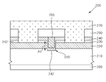
- FIG. 2 is a cross-sectional view schematically illustrating a nitride based transistor according to an exemplary embodiment of the present disclosure.
- FIG 3 is a schematic cross-sectional view of a nitride based transistor according to another exemplary embodiment of the present disclosure.
- FIG. 4 is a cross-sectional view schematically showing a nitride-based transistor according to another embodiment of the present disclosure.
- FIG. 5 is a cross-sectional view schematically illustrating a nitride-based transistor according to another embodiment of the present disclosure.
- FIG. 6 is a cross-sectional view schematically illustrating a nitride-based transistor according to another embodiment of the present disclosure.
- FIG. 7 is a schematic cross-sectional view of a nitride based transistor according to another exemplary embodiment of the present disclosure.
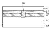
- FIGS. 8 to 13 are cross-sectional views schematically illustrating a method of manufacturing a nitride-based transistor according to an embodiment of the present disclosure.
- FIG. 14 is a view illustrating a method of manufacturing a nitride-based transistor according to another embodiment of the present disclosure.
- the term 'upper' or 'lower' is a relative concept set at an observer's viewpoint, and when the observer's viewpoint is different, 'upper' may mean 'lower', and 'lower' means 'upper'. It may mean.
- the term "vertical channel” may mean that the conduction of charge from the source electrode to the drain electrode includes a channel formed in the vertical direction. Accordingly, the vertical channel may be used to include not only the case in which the channel layer is formed perpendicular to the reference plane such as the substrate plane, but also the case in which the channel layer is inclined at a predetermined angle with respect to the reference plane.
- the source electrode and the drain electrode are named separately for convenience in consideration of the direction of the current.
- the source electrode is the drain electrode
- the drain electrode is the source. It may also mean an electrode.
- the interface region between the first layer and the second layer encompasses not only the junction interface between the first layer and the second layer, but also a predetermined internal region of the first layer or the second layer adjacent to the interface. Can be interpreted as
- the nitride based transistor 200 may include a first semiconductor layer 210, a second semiconductor layer 220, a third semiconductor layer 230, and a fourth semiconductor layer 240.
- the fourth semiconductor layer 240 is disposed along the inner wall of the trench 250 formed to penetrate the at least the second semiconductor layer 220 and the third semiconductor layer 230, and the fourth semiconductor layer 240.
- the nitride based transistor 200 includes a gate electrode 265 formed on the fourth semiconductor layer 240.
- the nitride-based transistor 200 may include a source electrode 270 electrically connected to the third semiconductor layer 230 or the fourth semiconductor layer 240, and a drain electrode electrically connected to the first semiconductor layer 210. 280).
- the first semiconductor layer 210 may be a first nitride-based semiconductor layer doped with a first type.
- the first type may be, for example, n-type or p-type.
- the dopant when doped with n-type, the dopant may be silicon (Si), and when doped with p-type, the dopant may be boron (B), arsenic (As), phosphorus (P), or magnesium (Mg). ) May be applied.
- the first semiconductor layer 210 may include a two-component system such as GaN or InN, a three-component system such as AlGaN or InGaN, or a four-component nitride semiconductor such as AlInGaN.
- the first semiconductor layer 210 may be an epitaxially grown GaN layer.
- the second semiconductor layer 220 may be a first nitride based semiconductor layer doped with a second type.
- the second type may be, for example, n-type or p-type, but means a different doping form from the first type. That is, when the first type is n type, the second type is p type, and when the first type is p type, the second type may be n type.
- the second semiconductor layer 220 may include a two-component system such as GaN or InN, a three-component system such as AlGaN or InGaN, or a four-component nitride semiconductor such as AlInGaN.
- the third semiconductor layer 230 may be the first nitride based semiconductor layer doped with the first type.
- the third semiconductor layer 230 may include a two-component system such as GaN or InN, a three-component system such as AlGaN or InGaN, or a four-component nitride semiconductor such as AlInGaN.
- the third semiconductor layer 230 may include a nitride semiconductor that is substantially the same as the first semiconductor layer 210.
- the fourth semiconductor layer 240 may be a second nitride semiconductor layer different from the first nitride semiconductor layer.
- the fourth semiconductor layer 240 may include a nitride having an energy band gap different from that of the nitride in the first semiconductor layer 210 to the third semiconductor layer 230.
- a 2DEG layer may be formed in an interface region.
- the first semiconductor layer 210 is an n-type GaN layer
- the second semiconductor layer 220 is a p-type GaN layer
- the third semiconductor layer 230 is an n-type GaN layer
- the fourth semiconductor layer 240 is an AlGaN layer
- the GaN layer has a smaller energy bandgap than the AlGaN layer, in heterojunction, a 2DEG layer can be formed in the GaN layer inner region from the bonding interface.
- the embodiments described below are illustrated to more clearly explain the spirit of the present disclosure, and include the first semiconductor layer 210, the second semiconductor layer 220, the third semiconductor layer 230, and the fourth semiconductor layer.
- the semiconductor layer 240 various nitride-based semiconductor layers other than the following embodiments may be applied.
- the nitride semiconductor of the first semiconductor layer 210 to the third semiconductor layer 230 may have a larger energy band gap than the nitride semiconductor of the fourth semiconductor layer 240.
- a portion of the fourth semiconductor layer 240 disposed on the bottom surface of the trench 250 may contact the first semiconductor layer 210.
- the 2DEG layer 242 may be formed in an inner region of the first semiconductor layer 210 near the interface between the first semiconductor layer 210 and the fourth semiconductor layer 240.
- a portion of the fourth semiconductor layer 240 disposed on the sidewall of the trench 250 may contact the second semiconductor 220 and the third semiconductor layer 230. Also, as shown in the drawing, when the trench 250 extends into the first semiconductor layer 210, a portion of the fourth semiconductor layer 240 may be further disposed on the sidewall of the trench 250. In this case, a portion of the fourth semiconductor layer 240 may contact the sidewalls of the first semiconductor layer 210 and the trench 250.
- a portion of the fourth semiconductor layer 240 formed on the sidewall of the trench 250 may include a portion of the fourth semiconductor layer 240 formed on the bottom surface of the trench 250 and a third semiconductor layer outside the trench 250. It may be thinner than a portion of the fourth semiconductor layer 240 formed on the 230.
- a 2DEG discontinuous region A1 may be formed in an interface region between the fourth semiconductor layer 240 and the first semiconductor layer 210 to the third semiconductor layer 230 on the sidewall of the trench 250.
- the a plane or m plane direction which is a direction perpendicular thereto, may have a low or no polarization effect. Accordingly, the 2DEG layer may not be formed in the interface region of the fourth semiconductor layer 240 and the first semiconductor layer 210 to the third semiconductor layer 230 on the sidewall of the trench 250.
- the 2DEG layer 242 may be formed in the interface region of the fourth semiconductor layer 240 and the third semiconductor layer 230 outside the trench 250.
- the gate electrode 265 may be formed on at least the fourth semiconductor layer 240 inside the trench 250, and may be formed to fill the inside of the trench 250 as shown. Although not shown, in some other embodiments, the gate electrode 265 may fill the inside of the trench 250 and may additionally exist in a pattern form on the fourth semiconductor layer 240 outside the trench 250.
- the gate electrode 265 may include a material forming a schottky junction with the fourth semiconductor layer 240.
- the gate electrode 265 may include a p-type GaN semiconductor doped with a dopant including boron (B), arsenic (As), phosphorus (P), magnesium (Mg), or a combination thereof.
- the gate electrode 265 may include a metal such as nickel (Ni) or gold (Au).
- an insulating film may be additionally disposed between the gate electrode 265 and the fourth semiconductor layer 240. The insulating film may function as a gate dielectric layer in relation to the gate electrode 265. When the insulating layer is interposed, the gate electrode 265 may include various conductors regardless of the Schottky junction.
- the gate electrode 265 may form a vertical channel in the second semiconductor layer 220 in contact with the fourth semiconductor layer 240 when the nitride transistor 200 is turned on.
- the channel may overcome the 2DEG discontinuous region A1 to allow charge conduction between the third semiconductor layer 230 and the first semiconductor layer 210. That is, in an embodiment of the present disclosure, when a voltage equal to or greater than a threshold voltage is applied to the gate electrode 265, a turn-on operation may be performed through the channel formed in the second semiconductor layer 220.
- the source electrode 270 may be insulated from the gate electrode 265 by the passivation layer 290 and disposed to contact the third semiconductor layer 230 or the fourth semiconductor layer 240.
- the source electrode 270 may be patterned to be in contact with side surfaces of the third semiconductor layer 230 and the fourth semiconductor layer 240 and disposed on the second semiconductor layer 220.
- the source electrode 270 may be disposed to contact the 2DEG layer 242 formed in the third semiconductor layer 230.
- the source electrode 270 may be patterned to be disposed only on the side surface of the fourth semiconductor layer 240 and disposed on the third semiconductor layer 230.
- the source electrode 270 may include a material capable of ohmic contact with the third semiconductor layer 230 or the fourth semiconductor layer 240.
- the source electrode 270 may include, for example, titanium (Ti), aluminum (Al), palladium (Pd), tungsten (W), or a combination thereof.
- the drain electrode 280 may be disposed under the first semiconductor layer 210, and may be disposed to face the source electrode 265 in the vertical direction.
- the drain electrode 280 may include a material capable of ohmic bonding with the first semiconductor layer 210.
- the drain electrode 280 may include titanium (Ti), aluminum (Al), palladium (Pd), tungsten (W), or a combination thereof.
- the 2DEG layer 242 is formed in the interface region between the fourth semiconductor layer 240 and the third semiconductor layer 230 outside the region and the trench 250.
- the 2DEG discontinuous region A1 is formed in the interface region between the fourth semiconductor layer 240 and the first semiconductor layer 210 to the third semiconductor layer 230 on the sidewall of the trench 250, thereby turning off. Can be maintained.
- a vertical channel is formed in the second semiconductor layer 220 to cover the 2DEG discontinuous region A1, so that charge may be conducted through the channel.
- a high concentration of charge in the 2DEG layer 242 formed through heterojunction between the nitride-based semiconductor layers is used for signal transmission, but is turned off when the gate voltage 265 is not applied. Can be maintained reliably. In the turn-on state, the high concentration of charge may be conducted through the vertical channel. As a result, it is possible to provide a nitride based transistor having a high current capacity and a low operating resistance and capable of reducing the chip size.
- FIG. 3 is a schematic cross-sectional view of a nitride based transistor according to another exemplary embodiment of the present disclosure.
- the nitride based transistor 300 is substantially the same as the nitride based transistor 200 described above with reference to FIG. 2 except that the side surface of the trench 255 has an inclination.
- the trench 255 may be inclined to further control the 2DEG discontinuous region in comparison with the nitride based transistor 200 of FIG. 2.
- the fourth semiconductor layer 240 and the first semiconductor layer 210 to the third semiconductor layer 230 formed along the inclined surface may be described.
- the 2DEG layer may be additionally formed in some inclined regions except for regions where the thickness of the fourth semiconductor layer 240 is relatively thin.
- nitride-based transistor 400 further includes a nitride film 410 including aluminum (Al) disposed between the fourth semiconductor layer 240 and the passivation layer 290. 2 and 3 are substantially the same as the nitride-based transistors 200 and 300 described above.
- the nitride film 410 including aluminum may be a thin film layer having a lattice constant different from the lattice constant of the fourth semiconductor layer 240.
- the nitride layer 410 may include, for example, an AlN layer, an InAlGaN layer, or an AlGaN layer having a higher Al concentration than the fourth semiconductor layer 240.
- the AlN layer, the InAlGaN layer, or the AlGaN layer having a higher Al concentration than the fourth semiconductor layer 240 is disposed on the fourth semiconductor layer 240.
- the strain at the interface between the AlGaN layer, which is the fourth semiconductor layer 240, and the GaN layer, which is the third semiconductor layer 230 may increase. Accordingly, the effect of the piezoelectric polarization at the interface may be increased to increase the density of the 2DEG layer at the interface region between the fourth semiconductor layer 240 and the third semiconductor layer 230.
- FIG. 5 is a cross-sectional view schematically illustrating a nitride-based transistor according to another embodiment of the present disclosure.
- the nitride-based transistor 500 is further described with reference to FIGS. 2 to 4 except that the nitride-based transistor 500 further includes a nitride film 510 including aluminum in the fourth semiconductor layer 240. It is substantially the same as the transistors 200, 300, 400.
- the nitride film 510 including aluminum may be a thin film layer having a lattice constant different from that of the fourth semiconductor layer 290.
- the nitride layer 510 may include, for example, an AlN layer, an InAlGaN layer, or an AlGaN layer having a higher Al concentration than the fourth semiconductor layer 240.
- the nitride film 510 inside the fourth semiconductor layer 290 has a strain at an interface between the fourth semiconductor layer 240 and the third semiconductor layer 230. By increasing the density of the 2DEG layer. At least one layer of the nitride film 510 may be interposed in the fourth semiconductor layer 290.
- FIG. 6 is a cross-sectional view schematically illustrating a nitride-based transistor according to another embodiment of the present disclosure.
- the drain electrode 282 is not disposed below the first semiconductor layer 210, but is disposed on the patterned first semiconductor layer 210. It is substantially the same as the nitride-based transistors 200, 300, 400, and 500 described above with reference to FIGS.
- the nitride based transistor 600 of FIG. 6 may have a semi-vertical transistor structure.
- the nitride-based transistor 700 includes the nitride-based transistor described above with reference to FIGS. 2 to 6 except that the source electrode 770 is disposed in a pattern form on the fourth semiconductor layer 240. Substantially the same as (200, 300, 400, 500, 600). In contrast to the nitride based transistors 200, 300, 400, 500, and 600, the source electrode 770 may be disposed not to be in direct contact with the third insulating layer 230.
- FIG. 8 to 13 are cross-sectional views schematically illustrating a method of manufacturing a nitride-based transistor according to an embodiment of the present disclosure.
- the first nitride-based third semiconductor layer 230 doped in a form is sequentially formed.
- the substrate 201 may be, for example, a growth substrate such as a sapphire substrate, a GaN substrate, a SiC substrate, a Si substrate, or the like, but is not necessarily limited thereto, and the substrate 201 may satisfy other requirements for growing a nitride-based semiconductor layer. Substrates are also possible.
- the first nitride-based first semiconductor layer 210, the first nitride-based second semiconductor layer 220, and the first nitride-based third semiconductor layer 230 may be, for example, two-component systems such as undoped GaN or InN, or the like.
- a three-component nitride such as AlGaN or InGaN, or a four-component nitride semiconductor such as AlInGaN may be included.
- the first nitride-based first semiconductor layer 210, the first nitride-based second semiconductor layer 220, and the first nitride-based third semiconductor layer 230 may be doped with n-type or p-type, for example.
- the first type may be, for example, n-type or p-type.
- the dopant when doped with n-type, the dopant may be silicon (Si), and when doped with p-type, the dopant may be boron (B), arsenic (As), phosphorus (P), or magnesium (Mg). ) May be applied.
- the second type may be, for example, n-type or p-type, but means a different doping form from the first type. That is, when the first type is n-type, the second type may be p-type, and when the first type is p-type, the second type may be n-type.
- the method of forming the first nitride-based first semiconductor layer 210, the first nitride-based second semiconductor layer 220, and the first nitride-based third semiconductor layer 230 is, for example, a metal organic chemical vapor deposition method ( Metal Organic Chemical Vapor Deposition), Molecular Beam Epitaxy, Hydrogen Vapor Phase Epitaxy and the like can be applied.
- the first semiconductor layer 210 may be an n-type GaN layer
- the second semiconductor layer 220 may be a p-type GaN layer
- the third semiconductor layer 230 may be an n-type GaN layer.
- a nitride based buffer layer such as AlN, may be formed on the substrate 201 before forming the first nitride based first semiconductor layer 210.
- the buffer layer may serve as a nucleus layer for growing the first nitride based first semiconductor layer 210, and may mitigate the lattice constant mismatch between the substrate 201 and the first nitride based first semiconductor layer 210. Can be performed.
- a trench 250 penetrating at least the second semiconductor layer 220 and the third semiconductor layer 230 is formed.
- the bottom surface of the trench 250 may expose the first semiconductor layer 210.
- the sidewall portion of the trench 250 may be formed to be perpendicular to the bottom surface of the trench 250.
- the sidewall portion of the trench 250 may be inclined at a predetermined angle with the bottom surface of the trench 250.
- the method of forming the trench 250 may use, for example, dry etching, wet etching, or a combination thereof.
- a second nitride-based fourth semiconductor is disposed on the first semiconductor layer 210 to the third semiconductor layer 230 inside the trench 250 and the third semiconductor layer 230 outside the trench 250.
- the fourth semiconductor layer 240 may be a second nitride-based semiconductor layer different from the first nitride-based first to third semiconductor layers 210, 220, and 230.
- the fourth semiconductor layer 240 may include a nitride having an energy band gap different from that of the nitride in the first semiconductor layer 210 to the third semiconductor layer 230.
- a fourth semiconductor layer 240 may be an AlGaN layer.
- the 2DEG layer 242 may be formed in an interface region between the fourth semiconductor layer 240 and the first semiconductor layer 210 disposed on the bottom surface of the trench 250.
- the 2DEG layer 242 may be formed in the interface region between the fourth semiconductor layer 240 and the third semiconductor layer 230 outside the trench 250.
- the 2DEG discontinuous region A1 in which the 2DEG layer is disconnected is formed in the interface region of the first semiconductor layer 210 to the third semiconductor layer 230, which is in contact with the portion of the fourth semiconductor layer 240 formed on the sidewall of the trench 250. Can be formed.
- a method of regrowth the fourth semiconductor layer 240 from the first semiconductor layer 210 to the third semiconductor layer 230 may be applied.
- a method of regrowing the fourth semiconductor layer 240 may include metal organic chemical vapor deposition, molecular beam epitaxy, and hydrogenation vapor deposition. Epitaxy) and the like can be applied.
- the process conditions such as the temperature
- the portion of the fourth semiconductor layer 240 formed in the sidewall portion of the trench 250 is divided into the bottom surface of the trench 250 and the third semiconductor layer outside the trench 250. It may be formed thinner than the portion of the fourth semiconductor layer 240 formed on the 230.
- the gate conductive layer 260 is formed to fill the trench 250 in which the fourth semiconductor layer 240 is formed and cover the fourth semiconductor layer 240 outside the trench 250.
- the gate conductive layer 260 may be formed of a material forming a schottky junction with the fourth semiconductor layer 240.
- the gate conductive layer 260 may be formed from a dopant-doped P-type GaN semiconductor including boron (B), arsenic (As), phosphorus (P), magnesium (Mg), or a combination thereof. have.
- the gate conductive layer 260 may be formed from a metal such as nickel (Ni) or gold (Au). In the process of forming the gate conductive layer 260, for example, an organic metal chemical vapor deposition method, a sputtering method, or the like may be applied.
- an insulating film may be formed on the fourth semiconductor layer 240 before the gate conductive layer 260 is formed.
- the insulating layer may be an oxide layer, a nitride layer, or an oxynitride layer.
- the insulating film can function as a gate dielectric layer in relation to a gate electrode described later.
- the gate conductive layer 260 is planarized to expose the fourth semiconductor layer 240 outside the trench 260, thereby forming the gate electrode 265 in the trench 250.
- the planarization process may include an etch back or a chemical physical polishing method.
- a passivation layer 290 is formed on the gate electrode 265 and the fourth semiconductor layer 240.
- the passivation layer 290 may include, for example, an oxide film, a nitride film, or an oxynitride film.
- the passivation layer 290 may be formed by, for example, a known method such as a deposition method or a coating method.
- the passivation layer 290, the fourth semiconductor layer 240, and the third semiconductor layer 230 are selectively patterned to form side surfaces of the fourth semiconductor layer 240 and the third semiconductor layer 230. Expose Subsequently, a conductive layer covering at least the fourth semiconductor layer 240 and the third semiconductor layer 230 having exposed sides is formed on the second semiconductor layer 220. As a result, the source electrode 270 can be formed.
- the source electrode 270 may include a material capable of ohmic contact with the third semiconductor layer 230 or the fourth semiconductor layer 240.
- the source electrode 270 may include, for example, titanium (Ti), aluminum (Al), palladium (Pd), tungsten (W), or a combination thereof. In the process of forming the source electrode 270, for example, an organometallic chemical vapor deposition method, a sputtering method, or the like may be applied.
- only the passivation layer 290 and the fourth semiconductor layer 240 may be selectively patterned to expose side surfaces of the fourth semiconductor layer 240. Subsequently, a source electrode 270 may be formed on the third semiconductor layer 230 to cover the fourth semiconductor layer 240 having exposed side surfaces.
- the substrate 201 may be removed from the first semiconductor layer 210.
- a laser-lift process may be applied to the separation process.
- a drain electrode 280 is formed on the first semiconductor layer 210.
- the drain electrode 280 may be disposed under the first semiconductor layer 210, and may be disposed to face the source electrode 270 in the vertical direction.
- the drain electrode 280 may include a material capable of ohmic bonding with the first semiconductor layer 210.
- the drain electrode 280 may include titanium (Ti), aluminum (Al), palladium (Pd), tungsten (W), or a combination thereof.
- an organic metal chemical vapor deposition method, a sputtering method, or the like may be applied to the process of forming the drain electrode 280.
- a nitride based transistor having a vertical channel can be manufactured.
- FIG. 14 is a view illustrating a method of manufacturing a nitride-based transistor according to another embodiment of the present disclosure.
- the gate conductive layer 260 is formed to fill the trench 250 in which the fourth semiconductor layer 240 is formed and cover the fourth semiconductor layer 240 outside the trench 250.
- the gate electrode 265 may be formed on the fourth semiconductor layer 240 while filling the trench 250.
- the process related to FIGS. 12 and 13 may be performed to manufacture a nitride-based transistor having a vertical channel.
- the fourth semiconductor layer 240 after forming the fourth semiconductor layer 240 in conjunction with FIGS. 8 to 10 and before forming the gate conductive layer 260, aluminum is included on the fourth semiconductor layer 240.
- a nitride film can be formed.
- the nitride film including aluminum may be a thin film layer having a lattice constant different from the lattice constant of the fourth semiconductor layer 240.
- the nitride layer may include, for example, an AlN layer, an InAlGaN layer, or a heavily doped AlGaN layer.
- the nitride layer may increase the effect of piezoelectric polarization at the interface between the fourth semiconductor layer 240 and the third semiconductor layer 230, thereby increasing the density of the 2DEG layer at the interface region.
- a process corresponding to FIGS. 11 to 13 described above may be performed to manufacture a nitride-based transistor having a vertical channel shown in FIG. 4.
- the nitride film including the aluminum may be formed to be interposed inside the fourth semiconductor layer 240.
- a nitride-based transistor having a vertical channel shown in FIG. 5 can be manufactured.
- the stack structure is patterned to expose the first semiconductor layer 210.
- the drain electrode 280 may be formed on the exposed first semiconductor layer 210.
- the source electrode may be formed on the fourth semiconductor layer 240 without forming the passivation layer 290. Can be. Thereafter, a passivation layer 290 may be formed between the source electrodes. As a result, a nitride-based transistor having a vertical channel shown in FIG. 7 can be manufactured.
Landscapes
- Junction Field-Effect Transistors (AREA)
Abstract
일 실시예에 따르는 질화물계 트랜지스터는 제1 형으로 도핑된 제1 질화물계 제1 반도체층, 상기 제1 반도체층 상에 배치되는 제2 형으로 도핑된 제1 질화물계 제2 반도체층, 상기 제2 반도체층 상에 배치되는 제1 형으로 도핑된 제1 질화물계 제3 반도체층, 적어도 상기 제2 반도체층 및 상기 제3 반도체층을 관통하도록 형성되는 트렌치의 내벽을 따라 배치되고 상기 트렌치 외부의 상기 제3 반도체층 상에 배치되는 제2 질화물계 제4 반도체층, 및 상기 제4 반도체층 상에 형성되는 게이트 전극을 포함한다. 상기 제2 질화물계 제4 반도체층은 상기 제1 질화물계 제1 반도체층 내지 제3 반도체층과 대비하여 다른 에너지 밴드갭을 가지는 질화물을 포함한다.
Description
본 개시(disclosure)는 대체로(generally) 질화물계 트랜지스터에 관한 것으로, 보다 상세하게는, 수직형 채널을 구비하는 질화물계 트랜지스터 및 이의 제조 방법에 관한 것이다.
정보통신기술의 발달로 인해, 고속 스위칭 환경이나 고전압 환경에서 동작하는 고내압 트랜지스터의 요청이 증가하고 있다. 이에, 최근에 등장한 질화갈륨계 트랜지스터는 종래의 실리콘 트랜지스터에 비해 고속 스위칭 동작이 가능하여 초고속 신호 처리에 적합할 뿐만 아니라 소재 자체의 고내압 특성에 의해 고전압 환경에 적합한 장점이 있어 업계의 주목을 받고 있다. 특히, HEMT(High Electron Mobility Transistor)의 경우, 이종 물질간 계면에서 발생하는 2DEG(2차원 전자가스, two-dimensional electron gas)를 이용함으로써, 전자의 이동도(mobility)를 높일 수 있어 고속 신호 전송에 적합한 장점이 있다.
도 1은 종래의 질화물계 트랜지스터의 일 예를 개략적으로 도시하는 단면도이다. 도면을 참조하면, 질화물계 트랜지스터(100)는 언도프(undoped) GaN 반도체층(110), AlGaN 반도체층(120), 소스 전극(130), 드레인 전극(140) 및 게이트 전극(150)을 구비할 수 있다. 상기 2DEG층(125)은 언도프 GaN 반도체층(110) 및 AlGaN 반도체층(120)의 경계면 부근에 형성된다. 이때, 게이트 전극(150)은 채널(125)을 통해 이동하는 전류 흐름을 제어할 수 있다.
그런데, 종래의 질화물계 반도체소자(100)에서는, 소자 동작 시에 게이트 전극(150)의 단부(Edge)에 전계(Electric Field)가 집중됨으로써 발생하는 항복 현상이 보고되고 있다. 이때, 항복 전압은 게이트(Gate)와 드레인(Drain) 사이의 거리(Lgd)에 비례하여 결정되며, 따라서, 항복 전압을 높이기 위해서는 게이트와 드레인 사이의 거리(Lgd)를 일정 거리 이상을 유지할 필요가 있다. 이로 인해, 칩 사이즈(Chip Size)를 감소시키는데 어려움이 있을 수 있다.
최근에는, 상술한 어려움을 극복하고 또한 칩 사이즈를 감소시키기 위해, 소스 전극과 드레인 전극을 기판의 맞은편에 각각 배치하는 질화물계 트랜지스터가 제안되고 있다. 일 예로서, 미국공개특허 2012-0319127에서는, 상술한 질화물계 트랜지스터의 일종으로서, 전류구멍수직전자트랜지스터(current aperture vertical electron transistor, 이하, CAVET)가 개시되고 있다. 상기 CAVET에서는 소스 전극과 드레인 전극 사이에 전류 장벽층으로서 P형 GaN층을 배치시키s고, 상기 P형 GaN층 사이의 구멍(Aperture)를 통해 전류가 흐르도록 구성하고 있다.
본 개시의 실시예는 높은 전류 용량, 낮은 동작 저항 및 높은 동작 신뢰성을 구비하는 수직형 채널을 구비하는 질화물계 트랜지스터를 제공한다.
본 개시의 실시예는 상기 수직형 채널을 구비하는 질화물계 트랜지스터의 제조 방법을 제공한다.
일 측면에 따르는 수직형 채널을 구비하는 질화물계 트랜지스터가 개시된다. 상기 질화물계 트랜지스터는 제1 형으로 도핑된 제1 질화물계 제1 반도체층, 상기 제1 반도체층 상에 배치되는 제2 형으로 도핑된 제1 질화물계 제2 반도체층, 상기 제2 반도체층 상에 배치되는 제1 형으로 도핑된 제1 질화물계 제3 반도체층, 적어도 상기 제2 반도체층 및 상기 제3 반도체층을 관통하도록 형성되는 트렌치의 내벽을 따라 배치되고 상기 트렌치 외부의 상기 제3 반도체층 상에 배치되는 제2 질화물계 제4 반도체층, 및 상기 제4 반도체층 상에 형성되는 게이트 전극을 포함한다. 상기 제2 질화물계 제4 반도체층은 상기 제1 질화물계 제1 반도체층 내지 제3 반도체층과 대비하여 다른 에너지 밴드갭을 가지는 질화물을 포함한다.
다른 측면에 따르는 수직형 채널을 구비하는 질화물계 트랜지스터의 제조 방법이 제공된다. 상기 질화물계 트랜지스터의 제조 방법에 있어서, 먼저, 기판 상에 제1 형으로 도핑된 제1 질화물계 제1 반도체층, 제2 형으로 도핑된 제1 질화물계 제2 반도체층 및 제1 형으로 도핑된 제1 질화물계 제3 반도체층을 순차적으로 형성한다. 적어도 상기 제2 반도체층 및 상기 제3 반도체층을 관통하는 트렌치를 형성한다. 상기 트렌치 내벽의 상기 제1 반도체층 내지 상기 제3 반도체층 및 상기 트렌치 외부의 상기 제3 반도체층 상에 제2 질화물계 제4 반도체층을 형성한다. 상기 트렌치 내부에 게이트 전극을 형성한다.
일 실시 예에 따르면, 질화물계 트랜지스터에서, 질화물계 반도체층간의 이종 접합을 통해 형성되는 2DEG층 내의 고농도의 전하를 신호 전달에 이용할 수 있다. 게이트 전압이 인가되지 않는 상태에서는 수직형 채널을 따라 2DEG층의 형성을 억제함으로써, 턴오프 상태를 신뢰성 있게 유지할 수 있도록 할 수 있다. 그리고, 상기 질화물계 트랜지스터의 턴온 상태에서는 수직형 채널을 통해 상기 고농도의 전하가 전도되도록 할 수 있다. 이로서, 높은 전류 용량과 낮은 동작 저항을 가지며, 아울러 칩 사이즈를 감소시킬 수 있는 수직형 채널을 구비하는 질화물계 트랜지스터를 제공할 수 있다.
도 1은 종래의 질화물계 트랜지스터의 일 예를 개략적으로 도시하는 단면도이다.
도 2는 본 개시의 일 실시 예에 따르는 질화물계 트랜지스터를 개략적으로 나타내는 단면도이다.
도 3은 본 개시의 다른 실시 예에 따르는 질화물계 트랜지스터를 개략적으로 나타내는 단면도이다.
도 4는 본 개시의 또다른 실시 예에 따르는 질화물계 트랜지스터를 개략적으로 나타내는 단면도이다.
도 5는 본 개시의 또다른 실시 예에 따르는 질화물계 트랜지스터를 개략적으로 나타내는 단면도이다.
도 6은 본 개시의 또다른 실시 예에 따르는 질화물계 트랜지스터를 개략적으로 나타내는 단면도이다.
도 7은 본 개시의 또다른 실시 예에 따르는 질화물계 트랜지스터를 개략적으로 나타내는 단면도이다.
도 8 내지 도 13은 본 개시의 일 실시 예에 따르는 질화물계 트랜지스터의 제조 방법을 개략적으로 나타내는 단면도이다.
도 14는 본 개시의 다른 실시 예에 따르는 질화물계 트랜지스터의 제조 방법을 나타내는 도면이다.
이하, 첨부한 도면들을 참조하여, 본 개시의 실시 예들을 보다 상세하게 설명하고자 한다. 그러나 본 개시에 개시된 기술은 여기서 설명되는 실시 예들에 한정되지 않고 다른 형태로 구체화될 수도 있다. 도면에서 각 장치의 구성요소를 명확하게 표현하기 위하여 상기 구성요소의 폭이나 두께 등의 크기를 다소 확대하여 나타내었다.
본 명세서에서 일 요소가 다른 요소 '위' 또는 '아래'에 위치하는 것으로 언급되는 경우, 이는 상기 일 요소가 다른 요소 '위' 또는 '아래'에 바로 위치하거나 또는 그들 요소들 사이에 추가적인 요소가 개재될 수 있다는 의미를 모두 포함한다. 본 명세서에서, '상부' 또는 '하부' 라는 용어는 관찰자의 시점에서 설정된 상대적인 개념으로, 관찰자의 시점이 달라지면, '상부' 가 '하부'를 의미할 수도 있고, '하부'가 '상부'를 의미할 수도 있다.
복수의 도면들 상에서 동일 부호는 실질적으로 서로 동일한 요소를 지칭한다. 또, 단수의 표현은 문맥상 명백하게 다르게 뜻하지 않는 한 복수의 표현을 포함하는 것으로 이해되어야 하고, '포함하다' 또는 '가지다' 등의 용어는 기술되는 특징, 숫자, 단계, 동작, 구성요소, 부분품 또는 이들을 조합한 것이 존재함을 지정하려는 것이지, 하나 또는 그 이상의 다른 특징들이나 숫자, 단계, 동작, 구성요소, 부분품 또는 이들을 조합한 것들의 존재 또는 부가 가능성을 미리 배제하지 않는 것으로 이해되어야 한다.
본 명세서에서, 수직형 채널이라는 의미는, 소스 전극으로부터 드레인 전극으로의 전하의 전도가 상하 방향으로 이루어지는 채널을 구비한다는 것을 의미할 수 있다. 따라서, 수직형 채널은 채널층이 기판 면과 같은 기준면에 대하여 수직으로 형성되는 경우뿐만 아니라, 상기 채널층이 상기 기준면에 대하여 소정의 각도로 경사진 경우를 모두 포함하는 의미로 사용될 수 있다.
본 명세서에서, 소스 전극 및 드레인 전극은 전류의 방향을 고려하여, 편의상 구분하여 명명한 것으로서, 인가되는 전압 극성의 변화에 의해 전류 방향이 변화하는 경우, 소스 전극은 드레인 전극을, 드레인 전극은 소스 전극을 의미할 수도 있다.
본 명세서에서, 제1 층과 제2 층 사이의 계면 영역이라 함은, 제1 층과 제2 층의 접합 계면뿐만 아니라, 계면과 인접하는 제1 층 또는 제2 층의 소정의 내부 영역을 포괄하는 것으로 해석될 수 있다.
도 2는 본 개시의 일 실시 예에 따르는 질화물계 트랜지스터를 개략적으로 나타내는 단면도이다. 도 2를 참조하면, 질화물계 트랜지스터(200)은 제1 반도체층(210), 제2 반도체층(220), 제3 반도체층(230) 및 제4 반도체층(240)을 구비할 수 있다. 이때, 제4 반도체층(240)은 적어도 제2 반도체층(220) 및 제3 반도체층(230)을 관통하도록 형성되는 트렌치(250)의 내벽을 따라 배치되고, 또한, 제4 반도체층(240)은 트렌치(250) 외부의 제3 반도체층(230) 상에 배치된다. 질화물계 트랜지스터(200)는 제4 반도체층(240) 상에 형성되는 게이트 전극(265)을 구비한다. 또한, 질화물계 트랜지스터(200)은 제3 반도체층(230) 또는 제4 반도체층(240)과 전기적으로 연결되는 소스 전극(270)과 제1 반도체층(210)과 전기적으로 연결되는 드레인 전극(280)을 포함할 수 있다.
도면을 참조하면, 제1 반도체층(210)은 제1 형으로 도핑된 제1 질화물계 반도체층일 수 있다. 상기 제1 형은 일 예로서, n형 또는 p형 일 수 있다. 일 예로서, n형으로 도핑되는 경우, 도펀트는 실리콘(Si)이 적용될 수 있으며, p형으로 도핑되는 경우, 도펀트는 붕소(B), 비소(As), 인(P), 마그세슘(Mg) 등이 적용될 수 있다. 제1 반도체층(210)은 일 예로서, GaN또는 InN 등과 같은 2성분계, AlGaN 또는 InGaN 등과 같은 3성분계, AlInGaN과 같은 4성분계 질화물 반도체를 포함할 수 있다. 제1 반도체층(210)은 일 예로서, 에피 성장된 GaN층일 수 있다.
제2 반도체층(220)은 제2 형으로 도핑된 제1 질화물계 반도체층일 수 있다. 상기 제2 형은 일 예로서, n형 또는 p형일 수 있으나, 상기 제1 형과는 서로 다른 도핑 형태를 의미한다. 즉, 제1 형이 n형 경우 제2 형은 p형이고, 제1 형이 p형 인 경우 제2 형은 n형 일 수 있다. 제2 반도체층(220)은 일 예로서, GaN또는 InN 등과 같은 2성분계, AlGaN 또는 InGaN 등과 같은 3성분계, AlInGaN과 같은 4성분계 질화물 반도체를 포함할 수 있다.
제3 반도체층(230)은 상기 제1 형으로 도핑된 상기 제1 질화물계 반도체층일 수 있다. 제3 반도체층(230)은 일 예로서, GaN또는 InN 등과 같은 2성분계, AlGaN 또는 InGaN 등과 같은 3성분계, AlInGaN과 같은 4성분계 질화물 반도체를 포함할 수 있다. 제3 반도체층(230)은 제1 반도체층(210)과 실질적으로 동일한 질화물 반도체를 포함할 수 있다.
제4 반도체층(240)은 상기 제1 질화물계 반도체층과 다른 제2 질화물계 반도체층일 수 있다. 제4 반도체층(240)은 제1 반도체층(210) 내지 제3 반도체층(230) 내의 질화물이 가지는 에너지 밴드갭과 다른 에너지 밴드갭을 가지는 질화물을 포함할 수 있다. 상기 서로 다른 에너지 밴드갭을 갖는 질화물계 반도체층이 이종 접합될 때, 계면 영역에서는 2DEG층이 형성될 수 있다.
이하에서는, 일 실시 예로서, 제1 반도체층(210)이 n형 GaN층, 제2 반도체층(220)이 p형 GaN층, 제3 반도체층(230)이 n형 GaN층이고, 제4 반도체층(240)은 AlGaN층인 경우에 대하여 설명하도록 한다. GaN 층은 AlGaN층 보다 에너지 밴드갭이 작기 때문에, 이종 접합시 2DEG층은 접합 계면으로부터 GaN층 내부 영역에 형성될 수 있다. 다만, 이하에서 설명하는 실시예는 본 개시의 사상을 보다 명확하게 설명하기 위해 예시된 것으로서, 제1 반도체층(210), 제2 반도체층(220), 제3 반도체층(230) 및 제4 반도체층(240)으로서 이하의 실시 예와는 다른 다양한 질화물계 반도체층이 적용될 수도 있다. 마찬가지로, 이하의 실시 예와는 다르게, 제1 반도체층(210) 내지 제3 반도체층(230)의 질화물 반도체가 제4 반도체층(240)의 질화물 반도체보다 에너지 밴드갭이 클 수도 있다.
도면을 참조하면, 트렌치(250)의 바닥면에 배치되는 제4 반도체층(240)의 일부분은 제1 반도체층(210)과 접할 수 있다. 이때, 제1 반도체층(210)과 제4 반도체층(240)의 계면 인근의 제1 반도체층(210)의 내부 영역에 2DEG층(242)이 형성될 수 있다.
트렌치(250)의 측벽에 배치되는 제4 반도체층(240)의 일부분은 제2 반도체(220) 및 제3 반도체층(230)과 접할 수 있다. 또한, 도시된 바와 같이, 트렌치(250)가 제1 반도체층(210)의 내부로 연장된 경우, 제4 반도체층(240)의 일부분은 트렌치(250)의 측벽에 추가로 배치될 수 있다. 이때, 제4 반도체층(240)의 일부분은 제1 반도체층(210)과 트렌치(250)의 측벽 방향에서 접할 수 있다.
트렌치(250)의 측벽에 형성되는 제4 반도체층(240)의 부분은 트렌치(250)의 바닥면에 형성되는 제4 반도체층(240)의 부분 및 트렌치(250) 외부의 제3 반도체층(230) 상에 형성되는 제4 반도체층(240)의 부분보다 얇게 형성될 수 있다. 이 때, 트렌치(250)의 측벽의 제4 반도체층(240) 및 제1 반도체층(210) 내지 제3 반도체층(230) 사이의 계면 영역에는 2DEG 불연속 영역(A1)이 형성될 수 있다. 반드시 특정한 이론에 한정되어 설명되는 것은 아니지만, 제4 반도체층(240)의 두께가 충분히 얇은 경우, 접하는 제1 반도체층(210) 내지 제3 반도체층(230)과의 계면에서 압전분극 효과가 감소되어 2DEG층이 형성되지 않을 수 있다. 또는, 일반적으로, AlGaN층이 분극효과가 높은 GaN층의 c면 방향으로부터 성장되는 경우, 이에 수직하는 방향인 a면 또는 m면 방향은 분극효과가 낮거나 없을 수 있다. 이에 따라 트렌치(250) 측벽의 제4 반도체층(240)과 제1 반도체층(210) 내지 제3 반도체층(230)의 계면 영역에서는 2DEG층이 형성되지 않을 수 있다.
이와는 별도로, 트렌치(250) 외부의 제4 반도체층(240) 및 제3 반도체층(230)의 계면 영역에서는 2DEG층(242)이 형성될 수 있다.
게이트 전극(265)은 적어도 트렌치(250) 내부의 제4 반도체층(240) 상에 형성될 수 있으며, 도시된 바와 같이, 트렌치(250) 내부를 메우도록 형성될 수 있다. 도시되지는 않았지만, 다른 몇몇 실시 예들에 있어서, 게이트 전극(265)은 트렌치(250) 내부를 메우고, 트렌치(250) 외부의 제4 반도체층(240) 상에 추가적으로 패턴 형태로 존재할 수도 있다.
게이트 전극(265)은 제4 반도체층(240)과 쇼트키(schottky) 접합을 이루는 물질을 포함할 수 있다. 일 예로서, 게이트 전극(265)은 붕소(B), 비소(As), 인(P), 마그네슘(Mg) 또는 이들의 조합을 포함하는 도펀트가 도핑된 p형 GaN 반도체를 포함할 수 있다. 다른 예로서, 게이트 전극(265)은 니켈(Ni), 금(Au)등의 금속을 포함할 수 있다. 도시되지는 않았지만, 몇몇 다른 실시 예들에 따르면, 게이트 전극(265)과 제4 반도체층(240) 사이에는 절연막이 추가로 배치될 수 있다. 상기 절연막은 게이트 전극(265)과의 관계에서 게이트 유전층으로서 기능할 수 있다. 상기 절연막이 개재되는 경우, 게이트 전극(265)은 상기 쇼트키 접합과 무관하게 다양한 전도체를 포함할 수 있다.
게이트 전극(265)은 질화물 트랜지스터(200)의 턴온 시에, 제4 반도체층(240)과 접하는 제2 반도체층(220) 내에 수직형 채널을 형성할 수 있다. 상기 채널은 상기 2DEG 불연속 영역(A1)을 극복하여, 제3 반도체층(230)과 제1 반도체층(210) 사이에서, 전하 전도가 이루어지게 할 수 있다. 즉, 본 개시의 실시 예에서는 게이트 전극(265)에 문턱 전압 이상의 전압이 인가될 때, 제2 반도체층(220) 내에 형성되는 상기 채널을 통하여, 턴온 동작이 이루어질 수 있다.
소스 전극(270)은 패시베이션층(290)에 의해 게이트 전극(265)과 절연되며 제3 반도체층(230) 또는 제4 반도체층(240)과 접하도록 배치될 수 있다. 도시된 구조에서, 소스 전극(270)은 제3 반도체층(230) 및 제4 반도체층(240)의 측면과 접하도록 패터닝되어 제2 반도체층(220) 상에 배치될 수 있다. 이 때, 소스 전극(270)은 제3 반도체층(230) 내부에 형성된 2DEG층(242)과 접하도록 배치될 수 있다. 도시되지는 않았지만, 다른 실시 예에서, 소스 전극(270)은 제4 반도체층(240)의 측면만을 접하도록 패터닝되어 제3 반도체층(230) 상에 배치될 수도 있다.
소스 전극(270)은 제3 반도체층(230) 또는 제4 반도체층(240)과 오믹 접합(ohmic contact)할 수 있는 물질을 포함할 수 있다. 소스 전극(270)은 일 예로서, 타이타늄(Ti), 알루이늄(Al), 팔라듐(Pd), 텅스텐(W) 또는 이들의 조합을 포함할 수 있다.
드레인 전극(280)은 제1 반도체층(210) 하부에 배치됨으로써, 소스 전극(265)과 상하 방향으로 맞은 편에 배치될 수 있다. 드레인 전극(280)은 제1 반도체층(210)과 오믹 접합할 수 있는 물질을 포함할 수 있다. 드레인 전극(280)은 일 예로서, 타이타늄(Ti), 알루이늄(Al), 팔라듐(Pd), 텅스텐(W) 또는 이들의 조합을 포함할 수 있다.
상술한 본 개시의 일 실시 예에 따르면, 게이트 전극(265)에 전압을 인가하지 않는 상태에서, 트렌치(250) 하부면의 제4 반도체층(240)과 제1 반도체층(210) 사이의 계면 영역, 트렌치(250) 외부의 제4 반도체층(240)과 제3 반도체층(230) 사이의 계면 영역에 2DEG층(242)이 형성된다. 반면에, 트렌치(250) 측벽의 제4 반도체층(240)과 제1 반도체층(210) 내지 제3 반도체층(230) 사이의 계면 영역에는 2DEG 불연속 영역(A1)이 형성됨으로써, 턴오프 상태를 유지할 수 있다. 게이트 전극(265)에 문턱 전압 이상의 전압이 인가되면, 2DEG 불연속 영역(A1)을 커버하도록 제2 반도체층(220) 내에 수직형 채널이 형성되어, 전하가 상기 채널을 통해 전도될 수 있다. 이와 같이, 질화물계 트랜지스터 구조에서, 질화물계 반도체층간의 이종 접합을 통해 형성되는 2DEG층(242) 내의 고농도의 전하를 신호 전달에 이용하되, 게이트 전압(265)이 인가되지 않는 상태에서는 턴오프 상태를 신뢰성 있게 유지하도록 할 수 있다. 그리고, 턴온 상태에서는 상기 수직형 채널을 통해 상기 고농도의 전하가 전도되도록 할 수 있다. 이로서, 높은 전류 용량과 낮은 동작 저항을 가지며, 아울러 칩 사이즈를 감소시킬 수 있는 질화물계 트랜지스터를 제공할 수 있다.
도 3은 본 개시의 다른 실시 예에 따르는 질화물계 트랜지스터를 개략적으로 나타내는 단면도이다. 도 3을 참조하면, 질화물계 트랜지스터(300)는 트렌치(255)의 측면이 경사를 갖는 것을 제외하고는 도 2와 관련하여 상술한 질화물계 트랜지스터(200)와 실질적으로 동일하다. 도 3에 도시된 바와 같이, 트렌치(255)를 경사지게 형성함으로써, 도 2의 질화물계 트랜지스터(200)와 대비하여 2DEG 불연속 영역을 추가적으로 제어할 수 있다. 반드시 특정한 이론에 한정하여 설명되는 것은 아니지만, 트렌치(255)가 경사진 형태를 가지는 경우, 경사면을 따라 형성되는 제4 반도체층(240)과 제1 반도체층(210) 내지 제3 반도체층(230) 사이의 계면 영역에서의 자발 분극과 압전 분극의 효과는 수직 형태의 트렌치(250)인 경우와 대비하여 상대적으로 강하게 작용할 수 있다. 따라서, 제4 반도체층(240)의 두께가 상대적으로 얇은 영역을 제외한 일부 경사 영역에서 2DEG층이 추가로 형성될 수 있다.
도 4는 본 개시의 또다른 실시 예에 따르는 질화물계 트랜지스터를 개략적으로 나타내는 단면도이다. 도 4를 참조하면, 질화물계 트랜지스터(400)는 제4 반도체층(240)과 패시베이션층(290) 사이에 배치되는 알루미늄(Al)을 포함하는 질화막(410)을 더 포함하는 것을 제외하고는 도 2 및 도 3과 관련되어 상술한 질화물계 트랜지스터(200, 300)과 실질적으로 동일하다. 상기 알루미늄을 포함하는 질화막(410)은 제4 반도체층(240)의 격자 상수와 다른 격자 상수를 가지는 구조의 박막층일 수 있다. 일 예로서, 질화막(410)은 일 예로서, AlN층, InAlGaN층 또는 상기 제4 반도체층(240)보다 Al의 농도가 높은 AlGaN층을 포함할 수 있다. 반드시 특정한 이론에 한정되어 설명되는 것은 아니지만, 상기 AlN층, InAlGaN층, 또는 상기 제4 반도체층(240)보다 Al의 농도가 높은 AlGaN층이 제4 반도체층(240) 상에 배치될 때, 제4 반도체층(240)인 AlGaN층과 제3 반도체층(230)인 GaN층의 계면에서의 변형률(strain)이 증가될 수 있다. 이에 따라, 계면에서의 압전 분극의 효과를 증가시켜, 제4 반도체층(240)과 제3 반도체층(230) 사이의 계면 영역에서 2DEG 층의 밀도를 증가시킬 수 있다.
도 5는 본 개시의 또다른 실시 예에 따르는 질화물계 트랜지스터를 개략적으로 나타내는 단면도이다. 도 5를 참조하면, 질화물계 트랜지스터(500)는 제4 반도체층(240) 내부에 알루미늄을 포함하는 질화막(510)을 더 포함하는 것을 제외하고는 도 2 내지 도 4와 관련되어 상술한 질화물계 트랜지스터(200, 300, 400)와 실질적으로 동일하다. 상기 알루미늄을 포함하는 질화막(510)은 제4 반도체층(290)의 격자 상수와 다른 격자 상수를 가지는 구조의 박막층일 수 있다. 일 예로서, 질화막(510)은 일 예로서, AlN층, InAlGaN층 또는 상기 제4 반도체층(240)보다 Al의 농도가 높은 AlGaN층을 포함할 수 있다. 도 4의 질화물계 트랜지스터(400)에서와 같이, 제4 반도체층(290) 내부의 질화막(510)은 제4 반도체층(240)과 제3 반도체층(230)의 계면에서의 변형률(strain)을 증가시켜, 2DEG층의 밀도를 증가시킬 수 있다. 질화막(510)은 제4 반도체층(290) 내부에 적어도 한 층 이상 개재될 수 있다.
도 6은 본 개시의 또다른 실시 예에 따르는 질화물계 트랜지스터를 개략적으로 나타내는 단면도이다. 도 6을 참조하면, 질화물계 트랜지스터(600)는 드레인 전극(282)이 제1 반도체층(210) 하부에 배치되지 않고, 패터닝된 제1 반도체층(210)상에 배치되는 것을 제외하고는 도 2 내지 도 5와 관련하여 상술한 질화물계 트랜지스터(200, 300, 400, 500)와 실질적으로 동일하다. 도 6의 질화물계 트랜지스터(600)는 세미(semi)-수직형 형태의 트랜지스터 구조일 수 있다.
도 7은 본 개시의 또다른 실시 예에 따르는 질화물계 트랜지스터를 개략적으로 나타내는 단면도이다. 도 7을 참조하면, 질화물계 트랜지스터(700)는 소스 전극(770)이 제4 반도체층(240) 상에 패턴 형태로 배치되는 것을 제외하고는 도 2 내지 도 6과 관련하여 상술한 질화물계 트랜지스터(200, 300, 400, 500, 600)과 실질적으로 동일하다. 질화물계 트랜지스터(200, 300, 400, 500, 600)과 대비할 때, 소스 전극(770)은 제3 절연층(230)과 직접 접하지 않도록 배치될 수 있다.
도 8 내지 도 13은 본 개시의 일 실시 예에 따르는 질화물계 트랜지스터의 제조 방법을 개략적으로 나타내는 단면도이다. 도 8을 참조하면, 기판(201) 상에 제1 형으로 도핑된 제1 질화물계 제1 반도체층(210), 제2 형으로 도핑된 제1 질화물계 제2 반도체층(220) 및 제1 형으로 도핑된 제1 질화물계 제3 반도체층(230)을 순차적으로 형성한다. 기판(201)은 일 예로서, 사파이어 기판, GaN 기판, SiC 기판, Si 기판 등과 같은 성장 기판일 수 있으나, 반드시 이에 한정되지는 않고, 질화물계 반도체층을 성장시킬 수 있는 요건을 만족시키는 한 다른 기판도 가능하다.
제1 질화물계 제1 반도체층(210), 제1 질화물계 제2 반도체층(220) 및 제1 질화물계 제3 반도체층(230)은 일 예로서, 언도프 GaN 또는 InN 등과 같은 2성분계, AlGaN 또는 InGaN 등과 같은 3성분계, AlInGaN과 같은 4성분계 질화물 반도체를 포함할 수 있다. 또한, 제1 질화물계 제1 반도체층(210), 제1 질화물계 제2 반도체층(220) 및 제1 질화물계 제3 반도체층(230)은 일 예로서, n형 또는 p형으로 도핑된 질화물계 반도체 물질을 포함할 수 있다. 상기 제1 형은 일 예로서, n형 또는 p형 일 수 있다. 일 예로서, n형으로 도핑되는 경우, 도펀트는 실리콘(Si)이 적용될 수 있으며, p형으로 도핑되는 경우, 도펀트는 붕소(B), 비소(As), 인(P), 마그세슘(Mg) 등이 적용될 수 있다. 상기 제2 형은 일 예로서, n형 또는 p형일 수 있으나, 상기 제1 형과는 서로 다른 도핑 형태를 의미한다. 즉, 제1 형이 n형 경우 제2 형은 p형이고, 제1 형이 p형 인 경우 제2 형은 n형 일 수 있다. 제1 질화물계 제1 반도체층(210), 제1 질화물계 제2 반도체층(220) 및 제1 질화물계 제3 반도체층(230)을 형성하는 방법은 일 예로서, 금속유기화학기상증착법(Metal Organic Chemical Vapor Deposition), 분자빔에피탁시(Molecular Beam Epitaxy), 수소화기상증착에피탁시(Hydride Vapor Phase Epitaxy) 등과 같은 방법을 적용할 수 있다. 일 실시 예에 있어서, 제1 반도체층(210)은 n형 GaN층, 제2 반도체층(220)은 p형 GaN층, 제3 반도체층(230)은 n형 GaN층일 수 있다.
도시되지는 않았지만, 몇몇 다른 실시예에 있어서, 제1 질화물계 제1 반도체층(210)을 형성하기 전에, 기판(201) 상에 일 예로서, AlN과 같은 질화물계 버퍼층을 형성할 수 있다. 상기 버퍼층은 제1 질화물계 제1 반도체층(210)을 성장하도록 하는 핵층의 역할을 할 수 있고, 기판(201)과 제1 질화물계 제1 반도체층(210) 간의 격자상수 불일치를 완화시키는 역할을 수행할 수 있다.
도 9를 참조하면, 적어도 제2 반도체층(220) 및 제3 반도체층(230)을 관통하는 트렌치(250)를 형성한다. 도시된 바와 같이, 트렌치(250)의 바닥면은 제1 반도체층(210)을 노출시킬 수 있다. 트렌치(250)의 측벽부는 트렌치(250)의 바닥면과 수직을 이루도록 형성될 수 있다. 또는 도 3의 실시예와 같이, 트렌치(250)의 측벽부는 트렌치(250)의 바닥면과 소정의 각도로 경사를 이룰 수도 있다. 트렌치(250)를 형성하는 방법은 일 예로서, 건식 식각, 습식 식각 또는 이들의 결합을 적용할 수 있다.
도 10을 참조하면, 트렌치(250) 내부의 제1 반도체층(210) 내지 제3 반도체층(230) 및 트렌치(250) 외부의 제3 반도체층(230) 상에 제2 질화물계 제4 반도체층(240)을 형성한다. 제4 반도체층(240)은 상기 제1 질화물계 제1 반도체층 내지 제3 반도체층(210, 220, 230)과 다른 제2 질화물계 반도체층일 수 있다. 제4 반도체층(240)은 제1 반도체층(210) 내지 제3 반도체층(230) 내의 질화물이 가지는 에너지 밴드갭과 다른 에너지 밴드갭을 가지는 질화물을 포함할 수 있다. 일 실시 예에 있어서, 제1 반도체층(210)이 n형 GaN층, 제2 반도체층(220)이 p형 GaN층, 제3 반도체층(230)이 n형 GaN층일 때, 제4 반도체층(240)은 AlGaN층일 수 있다.
트렌치(250)의 바닥면에 배치되는 제4 반도체층(240)과 제1 반도체층(210)의 계면 영역에는 2DEG층(242)이 형성될 수 있다. 또한, 트렌치(250) 외부의 제4 반도체층(240) 및 제3 반도체층(230)의 계면 영역에서는 2DEG층(242)이 형성될 수 있다. 트렌치(250)의 측벽에 형성되는 제4 반도체층(240)의 부분과 접하는 제1 반도체층(210) 내지 제3 반도체층(230)의 계면 영역에는 2DEG층이 단절된 2DEG 불연속 영역(A1)이 형성될 수 있다.
제2 질화물계 제4 반도체층(240)을 형성하는 방법은 제1 반도체층(210) 내지 제3 반도체층(230)로부터 제4 반도체층(240)을 재성장(regrowth)시키는 방법을 적용할 수 있다. 제4 반도체층(240)을 재성장시키는 방법은 일 예로서, 금속유기화학기상증착법(Metal Organic Chemical Vapor Deposition), 분자빔에피탁시(Molecular Beam Epitaxy), 수소화기상증착에피탁시(Hydride Vapor Phase Epitaxy) 등과 같은 방법을 적용할 수 있다. 이때, 온도와 같은 공정 조건을 제어함으로써, 트렌치(250)의 측벽부에 형성되는 제4 반도체층(240)의 부분을, 트렌치(250)의 바닥면 및 트렌치(250) 외부의 제3 반도체층(230) 상에 형성되는 제4 반도체층(240)의 부분보다 얇게 형성할 수 있다.
도 10을 다시 참조하면, 제4 반도체층(240)이 형성된 트렌치(250) 내부를 채우고, 트렌치(250) 외부의 제4 반도체층(240)을 커버하도록 게이트 도전층(260)을 형성한다. 게이트 도전층(260)은 제4 반도체층(240)과 쇼트키(schottky) 접합을 이루는 물질로 형성될 수 있다. 일 예로서, 게이트 도전층(260)은 붕소(B), 비소(As), 인(P), 마그네슘(Mg) 또는 이들의 조합을 포함하는 도펀트가 도핑된 P-형 GaN 반도체로부터 형성될 수 있다. 다른 예로서, 게이트 도전층(260)은 니켈(Ni), 금(Au)등의 금속으로부터 형성될 수 있다. 게이트 도전층(260)을 형성하는 공정은 일 예로서, 유기금속화학기상증착법, 스퍼터링법 등과 같은 방법을 적용할 수 있다.
도시되지는 않았지만, 몇몇 다른 실시 예들에 있어서, 게이트 도전층(260)을 형성하기 전에, 제4 반도체층(240) 상에 절연막을 형성할 수 있다. 상기 절연막은 일 예로서, 산화막, 질화막 또는 산질화막일 수 있다. 상기 절연막은 후술하는 게이트 전극과의 관계에서 게이트 유전층으로서 기능할 수 있다.
도 11을 참조하면, 게이트 도전층(260)을 평탄화하여 트렌치(260) 외부의 제4 반도체층(240)을 노출시킴으로써, 트렌치(250) 내부에 게이트 전극(265)을 형성한다. 상기 평탄화 공정은 일 예로서, 에치백 또는 화학적물리적연마법 등을 적용할 수 있다.
도 12를 참조하면, 게이트 전극(265) 및 제4 반도체층(240) 상에 패시베이션층(290)을 형성한다. 패시베이션층(290)은 일예로서, 산화막, 질화막 또는 산질화막을 포함할 수 있다. 패시베이션층(290)은 일 예로서, 증착법, 코팅법 등의 공지의 방법에 의해 형성될 수 있다.
도 13을 참조하면, 패시베이션층(290), 제4 반도체층(240) 및 제3 반도체층(230)을 선택적으로 패터닝하여, 제4 반도체층(240) 및 제3 반도체층(230)의 측면을 노출시킨다. 이어서, 측면이 노출된 제4 반도체층(240) 및 제3 반도체층(230)을 적어도 커버하는 전도층을 제2 반도체층(220) 상에 형성한다. 이로서, 소스 전극(270)을 형성할 수 있다. 소스 전극(270)은 제3 반도체층(230) 또는 제4 반도체층(240)과 오믹 접합(ohmic contact)할 수 있는 물질을 포함할 수 있다. 소스 전극(270)은 일 예로서, 타이타늄(Ti), 알루이늄(Al), 팔라듐(Pd), 텅스텐(W) 또는 이들의 조합을 포함할 수 있다. 소스 전극(270)을 형성하는 공정은 일 예로서, 유기금속화학기상증착법, 스퍼터링법 등과 같은 방법을 적용할 수 있다.
도시된 것과 다른 몇몇 다른 실시예에 따르면, 패시베이션층(290) 및 제4 반도체층(240) 만을 선택적으로 패터닝하여, 제4 반도체층(240)의 측면을 노출시킬 수 있다. 이어, 측면이 노출된 제4 반도체층(240)을 커버하는 소스 전극(270)을 제3 반도체층(230) 상에 형성할 수도 있다.
이어서, 기판(201)을 제1 반도체층(210)과 분리하여 제거할 수 있다. 상기 분리공정은 일 예로서, 레이저-리프트 공정을 적용할 수 있다, 제1 반도체층(210) 상에 드레인 전극(280)을 형성한다. 드레인 전극(280)은 제1 반도체층(210) 하부에 배치됨으로써, 소스 전극(270)과 상하 방향으로 맞은 편에 배치될 수 있다. 드레인 전극(280)은 제1 반도체층(210)과 오믹 접합할 수 있는 물질을 포함할 수 있다. 드레인 전극(280)은 일 예로서, 타이타늄(Ti), 알루이늄(Al), 팔라듐(Pd), 텅스텐(W) 또는 이들의 조합을 포함할 수 있다. 드레인 전극(280)을 형성하는 공정은 일 예로서, 유기금속화학기상증착법, 스퍼터링법 등과 같은 방법을 적용할 수 있다. 상술한 공정을 통하여 수직형 채널을 구비하는 질화물계 트랜지스터를 제조할 수 있다.
도 14는 본 개시의 다른 실시 예에 따르는 질화물계 트랜지스터의 제조 방법을 나타내는 도면이다. 먼저, 도 8 내지 도 10과 관련되어 상술된 공정을 진행한다. 즉, 제4 반도체층(240)이 형성된 트렌치(250) 내부를 채우고, 트렌치(250) 외부의 제4 반도체층(240)을 커버하도록 게이트 도전층(260)을 형성한다. 이어서, 제4 반도체층(240) 상에서, 게이트 도전층(260)을 패터닝함으로써, 트렌치(250) 내부를 채우며 제4 반도체층(240) 상에 배치되는 게이트 전극(265)을 형성할 수 있다. 이후에, 도 12 및 도 13과 관련된 공정을 진행하여 수직형 채널을 구비하는 질화물계 트랜지스터를 제조할 수 있다.
몇몇 다른 실시 예들에 있어서는, 도 8 내지 도 10와 관련되어 제4 반도체층(240)을 형성한 후, 게이트 도전층(260)을 형성하기 전에, 제4 반도체층(240) 상에 알루미늄을 포함하는 질화막을 형성할 수 있다. 상기 알루미늄을 포함하는 질화막은 제4 반도체층(240)의 격자 상수와 다른 격자 상수를 가지는 구조의 박막층일 수 있다. 일 예로서, 상기 질화막은 일 예로서, AlN층, InAlGaN층 또는 고농도로 도핑된 AlGaN층을 포함할 수 있다. 상기 질화막은 제4 반도체층(240)과 제3 반도체층(230) 사이 계면에서의 압전 분극의 효과를 증가시켜, 계면 영역에서의 2DEG 층의 밀도를 증가시킬 수 있다. 이후에, 상술한 도 11 내지 도 13에 대응되는 공정을 진행하여, 도 4에 도시된 수직형 채널을 구비하는 질화물계 트랜지스터를 제조할 수 있다.
몇몇 다른 실시 예들에 있어서는, 상기 알루미늄을 포함하는 질화막은 제4 반도체층(240)의 내부에 개재되도록 형성될 수도 있다. 이로서, 도 5에 도시되는 수직형 채널을 구비하는 질화물계 트랜지스터를 제조할 수 있다.
몇몇 다른 실시 예들에 있어서는, 도 8 내지 도 13과 관련되어 소스 전극(270)을 구비하는 적층 구조물을 형성한 후에, 상기 적층 구조물을 패터닝하여 제1 반도체층(210)을 노출시킨다. 그리고, 드레인 전극(280)을 노출된 제1 반도체층(210)에 형성할 수 있다. 이로서, 도 6에 도시되는 수직형 채널을 구비하는 질화물계 트랜지스터를 제조할 수 있다.
몇몇 다른 실시 예들에 있어서는, 도 8 내지 도 11과 관련되어 게이트 전극(265)을 형성한 후에, 패시베이션층(290)을 형성하지 않고, 소스 전극을 제4 반도체층(240) 상에서 패터닝하여 형성할 수 있다. 이후에, 패시베이션층(290)이 상기 소스 전극 사이에 형성할 수 있다. 이로서, 도 7에 도시되는 수직형 채널을 구비하는 질화물계 트랜지스터를 제조할 수 있다.
이상에서는 도면 및 실시 예를 참조하여 설명하였지만, 해당 기술 분야의 숙련된 당업자는 하기의 특허청구범위에 기재된 본 출원의 기술적 사상으로부터 벗어나지 않는 범위 내에서 본 출원에 개시된 실시예들을 다양하게 수정 및 변경시킬 수 있음을 이해할 수 있을 것이다.
Claims (26)
- 제1 형으로 도핑된 제1 질화물계 제1 반도체층;상기 제1 반도체층 상에 배치되는 제2 형으로 도핑된 제1 질화물계 제2 반도체층;상기 제2 반도체층 상에 배치되는 제1 형으로 도핑된 제1 질화물계 제3 반도체층;적어도 상기 제2 반도체층 및 상기 제3 반도체층을 관통하도록 형성되는 트렌치의 내벽을 따라 배치되고, 상기 트렌치 외부의 상기 제3 반도체층 상에 배치되는 제2 질화물계 제4 반도체층; 및상기 제4 반도체층 상에 형성되는 게이트 전극을 포함하되,상기 제2 질화물계 제4 반도체층은 상기 제1 질화물계 제1 반도체층 내지 제3 반도체층과 대비하여 다른 에너지 밴드갭을 가지는 질화물을 포함하는수직형 채널을 구비하는 질화물계 트랜지스터.
- 제1 항에 있어서,상기 트렌치의 바닥면에 배치되는 제4 반도체층과 상기 제1 반도체층의 계면영역에 이종 접합에 의한 2DEG가 형성되는수직형 채널을 구비하는 질화물계 트랜지스터.
- 제1 항에 있어서,상기 제3 반도체층과 상기 제4 반도체층 사이의 계면 영역에 이종 접합에 의한 2DEG가 형성되는수직형 채널을 구비하는 질화물계 트랜지스터.
- 제1 항에 있어서,상기 제1 반도체층과 전기적으로 연결되는 드레인 전극 및 상기 제3 반도체층 또는 상기 제4 반도체층과 전기적으로 연결되는 소스 전극을 더 포함하는수직형 채널을 구비하는 질화물계 트랜지스터.
- 제1 항에 있어서,상기 트렌치의 측벽부는 상기 트렌치의 바닥면과 수직을 이루는수직형 채널을 구비하는 질화물계 트랜지스터.
- 제1 항에 있어서,상기 트렌치의 측벽부는 상기 트렌치의 바닥면과 소정의 각도로 경사를 이루는수직형 채널을 구비하는 질화물계 트랜지스터.
- 제1 항에 있어서,상기 트렌치의 측벽부에 형성되는 상기 제4 반도체층의 부분은 상기 트렌치의 바닥면에 형성되는 상기 제4 반도체층의 부분 및 상기 트렌치 외부의 상기 제3 반도체층 상에 형성되는 상기 제4 반도체층의 부분보다 두께가 얇은수직형 채널을 구비하는 질화물계 트랜지스터.
- 제1 항에 있어서,상기 게이트 전극은, 턴온 시에, 상기 트렌치의 측벽의 상기 제4 반도체층과 상기 제2 반도체층의 계면 영역에 채널층을 형성하는수직형 채널을 구비하는 질화물계 트랜지스터.
- 제1 항에 있어서,상기 게이트 전극은상기 트렌치의 내부를 채우도록 배치되는수직형 채널을 구비하는 질화물계 트랜지스터.
- 제1 항에 있어서,상기 게이트 전극은상기 제4 반도체층과 쇼트키 접합을 이루는수직형 채널을 구비하는 질화물계 트랜지스터.
- 제1 항에 있어서,상기 게이트 전극과 상기 제4 반도체층 사이에 배치되는 절연막을 더 포함하는수직형 채널을 구비하는 질화물계 트랜지스터.
- 제1 항에 있어서,상기 제4 반도체층 상에 배치되고, 상기 제4 반도체층의 격자 상수와 다른 격자 상수를 가지는 구조의 질화막을 더 포함하는수직형 채널을 구비하는 질화물계 트랜지스터.
- 제1 항에 있어서,상기 제4 반도체층 내부에 개재되고, 상기 제4 반도체층의 격자 상수와 다른 격자 상수를 가지는 구조의 질화막을 더 포함하는수직형 채널을 구비하는 질화물계 트랜지스터.
- 제1 항에 있어서,상기 제1 반도체층은 n형으로 도핑된 GaN층이고,상기 제2 반도체층은 p형으로 도핑된 GaN층이고,상기 제3 반도체층은 n형으로 도핑된 GaN층이고,상기 제4 반도체층은 AlGaN층인수직형 채널을 구비하는 질화물계 트랜지스터.
- 제14 항에 있어서,상기 제4 반도체층 상에 배치되며, AlN층, InAlGaN층 및 상기 제4 반도체층보다 Al의 농도가 높은 AlGaN층으로 이루어진 그룹에서 선택된 적어도 하나를 더 포함하는수직형 채널을 구비하는 질화물계 트랜지스터.
- 제14 항에 있어서,상기 제4 반도체층 내부에 개재되고, AlN층, InAlGaN층 및 상기 제4 반도체층보다 Al의 농도가 높은 AlGaN층으로 이루어진 그룹에서 선택된 적어도 하나를 더 포함하는수직형 채널을 구비하는 질화물계 트랜지스터.
- 기판 상에 제1 형으로 도핑된 제1 질화물계 제1 반도체층, 제2 형으로 도핑된 제1 질화물계 제2 반도체층 및 제1 형으로 도핑된 제1 질화물계 제3 반도체층을 순차적으로 형성하는 단계;적어도 상기 제2 반도체층 및 상기 제3 반도체층을 관통하는 트렌치를 형성하는 단계;상기 트렌치 내벽의 상기 제1 반도체층 내지 상기 제3 반도체층 및 상기 트렌치 외부의 상기 제3 반도체층 상에 제2 질화물계 제4 반도체층을 형성하는 단계; 및상기 트렌치 내부에 게이트 전극을 형성하는 단계를 포함하는수직형 채널을 구비하는 질화물계 트랜지스터의 제조 방법.
- 제17 항에 있어서,상기 제4 반도체층을 형성하는 단계는상기 제1 반도체층 내지 제3 반도체층로부터 상기 제4 반도체층을 재성장(regrowth)시키는 단계를 포함하는수직형 채널을 구비하는 질화물계 트랜지스터의 제조 방법.
- 제18 항에 있어서,상기 트렌치의 측벽부에 형성되는 상기 제4 반도체층의 부분은 상기 트렌치의 바닥면에 형성되는 상기 제4 반도체층의 부분 및 상기 트렌치 외부의 상기 제3 반도체층 상에 형성되는 상기 제4 반도체층의 부분보다 두께가 얇은수직형 채널을 구비하는 질화물계 트랜지스터의 제조 방법.
- 제17 항에 있어서,상기 트렌치의 측벽부는 상기 트렌치의 바닥면과 수직을 이루도록 형성하는수직형 채널을 구비하는 질화물계 트랜지스터의 제조 방법.
- 제17 항에 있어서,상기 트렌치의 측벽부는 상기 트렌치의 바닥면과 소정의 각도로 경사를 이루는수직형 채널을 구비하는 질화물계 트랜지스터의 제조 방법.
- 제17 항에 있어서,상기 게이트 전극을 형성하는 단계는상기 제4 반도체층이 형성된 상기 트렌치를 채우고, 상기 트렌치 외부의 상기 제4 반도체층 상에 게이트 도전층을 형성하는 단계; 및상기 트렌치 외부의 상기 제4 반도체층을 노출되도록 상기 게이트 도전층을 평탄화하는 단계를 포함하는수직형 채널을 구비하는 질화물계 트랜지스터의 제조 방법.
- 제22 항에 있어서,상기 게이트 도전층을 형성하기 전에, 상기 제4 반도체층 상에 절연막을 형성하는 단계를 더 포함하는수직형 채널을 구비하는 질화물계 트랜지스터의 제조 방법.
- 제17 항에 있어서,적어도 상기 제4 반도체층과 접하는 소스 전극을 형성하는 단계를 더 포함하는수직형 채널을 구비하는 질화물계 트랜지스터의 제조 방법.
- 제24 항에 있어서,상기 소스 전극을 형성하는 단계는상기 게이트 전극 상에 패시베이션층을 형성하는 단계;상기 패시베이션층, 상기 제4 반도체층 및 상기 제3 반도체층을 선택적으로 패터닝하여, 적어도 상기 제4 반도체층 및 상기 제3 반도체층의 측면을 노출시키는 단계; 및상기 적어도 노출된 제4 반도체층 및 제3 반도체층의 측면을 적어도 커버하는 전도층을 상기 제2 반도체층 상에 형성하는 단계를 포함하는수직형 채널을 구비하는 질화물계 트랜지스터의 제조 방법.
- 제17 항에 있어서,상기 제1 반도체층과 접하는 드레인 전극을 형성하는 단계를 더 포함하는수직형 채널을 구비하는 질화물계 트랜지스터의 제조 방법.
Applications Claiming Priority (2)
| Application Number | Priority Date | Filing Date | Title |
|---|---|---|---|
| KR10-2013-0069677 | 2013-06-18 | ||
| KR1020130069677A KR20140146849A (ko) | 2013-06-18 | 2013-06-18 | 수직형 채널을 구비하는 질화물계 트랜지스터 및 이의 제조 방법 |
Publications (1)
| Publication Number | Publication Date |
|---|---|
| WO2014204209A1 true WO2014204209A1 (ko) | 2014-12-24 |
Family
ID=52104868
Family Applications (1)
| Application Number | Title | Priority Date | Filing Date |
|---|---|---|---|
| PCT/KR2014/005371 Ceased WO2014204209A1 (ko) | 2013-06-18 | 2014-06-18 | 수직형 채널을 구비하는 질화물계 트랜지스터 및 이의 제조 방법 |
Country Status (2)
| Country | Link |
|---|---|
| KR (1) | KR20140146849A (ko) |
| WO (1) | WO2014204209A1 (ko) |
Cited By (1)
| Publication number | Priority date | Publication date | Assignee | Title |
|---|---|---|---|---|
| CN114127931A (zh) * | 2021-10-22 | 2022-03-01 | 英诺赛科(苏州)科技有限公司 | 氮化物基半导体装置及其制造方法 |
Families Citing this family (1)
| Publication number | Priority date | Publication date | Assignee | Title |
|---|---|---|---|---|
| KR102549356B1 (ko) * | 2021-10-15 | 2023-06-29 | 웨이브로드 주식회사 | 비발광 3족 질화물 반도체 적층체를 제조하는 방법 |
Citations (5)
| Publication number | Priority date | Publication date | Assignee | Title |
|---|---|---|---|---|
| US20090072240A1 (en) * | 2007-09-14 | 2009-03-19 | Transphorm Inc. | III-Nitride Devices with Recessed Gates |
| KR20090132533A (ko) * | 2008-06-20 | 2009-12-30 | 페어차일드 세미컨덕터 코포레이션 | 트렌치형 게이트 소자를 위한 두꺼운 저부 유전체의 구조 및 그 제조 방법 |
| CN102629624A (zh) * | 2012-04-29 | 2012-08-08 | 西安电子科技大学 | 基于GaN的MIS栅增强型HEMT器件及制作方法 |
| CN102683406A (zh) * | 2012-04-29 | 2012-09-19 | 西安电子科技大学 | GaN基的MS栅增强型高电子迁移率晶体管及制作方法 |
| JP2013077630A (ja) * | 2011-09-29 | 2013-04-25 | Fujitsu Ltd | 半導体装置及びその製造方法 |
-
2013
- 2013-06-18 KR KR1020130069677A patent/KR20140146849A/ko not_active Ceased
-
2014
- 2014-06-18 WO PCT/KR2014/005371 patent/WO2014204209A1/ko not_active Ceased
Patent Citations (5)
| Publication number | Priority date | Publication date | Assignee | Title |
|---|---|---|---|---|
| US20090072240A1 (en) * | 2007-09-14 | 2009-03-19 | Transphorm Inc. | III-Nitride Devices with Recessed Gates |
| KR20090132533A (ko) * | 2008-06-20 | 2009-12-30 | 페어차일드 세미컨덕터 코포레이션 | 트렌치형 게이트 소자를 위한 두꺼운 저부 유전체의 구조 및 그 제조 방법 |
| JP2013077630A (ja) * | 2011-09-29 | 2013-04-25 | Fujitsu Ltd | 半導体装置及びその製造方法 |
| CN102629624A (zh) * | 2012-04-29 | 2012-08-08 | 西安电子科技大学 | 基于GaN的MIS栅增强型HEMT器件及制作方法 |
| CN102683406A (zh) * | 2012-04-29 | 2012-09-19 | 西安电子科技大学 | GaN基的MS栅增强型高电子迁移率晶体管及制作方法 |
Cited By (3)
| Publication number | Priority date | Publication date | Assignee | Title |
|---|---|---|---|---|
| CN114127931A (zh) * | 2021-10-22 | 2022-03-01 | 英诺赛科(苏州)科技有限公司 | 氮化物基半导体装置及其制造方法 |
| WO2023065284A1 (en) * | 2021-10-22 | 2023-04-27 | Innoscience (Suzhou) Technology Co., Ltd. | Nitride-based semiconductor device and method for manufacturing the same |
| US12159931B2 (en) | 2021-10-22 | 2024-12-03 | Innoscience (Suzhou) Technology Co., Ltd. | Nitride-based semiconductor device and method for manufacturing the same |
Also Published As
| Publication number | Publication date |
|---|---|
| KR20140146849A (ko) | 2014-12-29 |
Similar Documents
| Publication | Publication Date | Title |
|---|---|---|
| US7884395B2 (en) | Semiconductor apparatus | |
| US9171946B2 (en) | Nitride semiconductor device and method of manufacturing the same | |
| JP4974454B2 (ja) | 半導体装置 | |
| EP3539159B1 (en) | Semiconductor devices with multiple channels and three-dimensional electrodes | |
| US8941148B2 (en) | Semiconductor device and method | |
| JP5386987B2 (ja) | 半導体装置 | |
| JP2017524247A (ja) | ショットキーダイオード及びその製造方法 | |
| CN213459743U (zh) | 高电子迁移率晶体管器件和电子器件 | |
| US10608102B2 (en) | Semiconductor device having a drain electrode contacting an epi material inside a through-hole and method of manufacturing the same | |
| CN112420850A (zh) | 一种半导体器件及其制备方法 | |
| US11127743B2 (en) | Transistor, semiconductor device, electronic apparatus, and method for producing transistor | |
| CN108352408B (zh) | 半导体装置、电子部件、电子设备以及半导体装置的制造方法 | |
| WO2020007265A1 (en) | Nitride power device with cap regions and manufacturing method thereof | |
| WO2014204209A1 (ko) | 수직형 채널을 구비하는 질화물계 트랜지스터 및 이의 제조 방법 | |
| KR20140141126A (ko) | 전계 완화부를 구비하는 질화물계 트랜지스터 및 이의 제조 방법 | |
| TWI794599B (zh) | 高電子遷移率電晶體及其製作方法 | |
| CN111834453B (zh) | 一种半导体器件及其制备方法 | |
| KR20150012019A (ko) | 질화물계 트랜지스터 및 이의 제조 방법 | |
| US12136675B2 (en) | Enhancement-mode device and preparation method therefor | |
| CN113451403B (zh) | 高电子迁移率晶体管及其制作方法 | |
| TWI795022B (zh) | 高電子遷移率電晶體 | |
| CN222674846U (zh) | 氮化镓功率器件 | |
| KR101480068B1 (ko) | 질화물 반도체 소자 및 그 제조방법 | |
| US20250234613A1 (en) | Gallium nitride power devices using nanosheet-typed channel layers | |
| WO2016208864A1 (ko) | 노멀리-오프를 구현하는 질화물계 트랜지스터 |
Legal Events
| Date | Code | Title | Description |
|---|---|---|---|
| 121 | Ep: the epo has been informed by wipo that ep was designated in this application |
Ref document number: 14813277 Country of ref document: EP Kind code of ref document: A1 |
|
| NENP | Non-entry into the national phase |
Ref country code: DE |
|
| 122 | Ep: pct application non-entry in european phase |
Ref document number: 14813277 Country of ref document: EP Kind code of ref document: A1 |