US7884395B2 - Semiconductor apparatus - Google Patents
Semiconductor apparatus Download PDFInfo
- Publication number
- US7884395B2 US7884395B2 US12/145,980 US14598008A US7884395B2 US 7884395 B2 US7884395 B2 US 7884395B2 US 14598008 A US14598008 A US 14598008A US 7884395 B2 US7884395 B2 US 7884395B2
- Authority
- US
- United States
- Prior art keywords
- layer
- nitride semiconductor
- silicon layer
- semiconductor layer
- silicon
- Prior art date
- Legal status (The legal status is an assumption and is not a legal conclusion. Google has not performed a legal analysis and makes no representation as to the accuracy of the status listed.)
- Expired - Fee Related, expires
Links
Images


Classifications
-
- H—ELECTRICITY
- H10—SEMICONDUCTOR DEVICES; ELECTRIC SOLID-STATE DEVICES NOT OTHERWISE PROVIDED FOR
- H10D—INORGANIC ELECTRIC SEMICONDUCTOR DEVICES
- H10D30/00—Field-effect transistors [FET]
- H10D30/40—FETs having zero-dimensional [0D], one-dimensional [1D] or two-dimensional [2D] charge carrier gas channels
- H10D30/47—FETs having zero-dimensional [0D], one-dimensional [1D] or two-dimensional [2D] charge carrier gas channels having two-dimensional [2D] charge carrier gas channels, e.g. nanoribbon FETs or high electron mobility transistors [HEMT]
- H10D30/471—High electron mobility transistors [HEMT] or high hole mobility transistors [HHMT]
- H10D30/475—High electron mobility transistors [HEMT] or high hole mobility transistors [HHMT] having wider bandgap layer formed on top of lower bandgap active layer, e.g. undoped barrier HEMTs such as i-AlGaN/GaN HEMTs
-
- H—ELECTRICITY
- H10—SEMICONDUCTOR DEVICES; ELECTRIC SOLID-STATE DEVICES NOT OTHERWISE PROVIDED FOR
- H10D—INORGANIC ELECTRIC SEMICONDUCTOR DEVICES
- H10D62/00—Semiconductor bodies, or regions thereof, of devices having potential barriers
- H10D62/10—Shapes, relative sizes or dispositions of the regions of the semiconductor bodies; Shapes of the semiconductor bodies
- H10D62/102—Constructional design considerations for preventing surface leakage or controlling electric field concentration
- H10D62/103—Constructional design considerations for preventing surface leakage or controlling electric field concentration for increasing or controlling the breakdown voltage of reverse-biased devices
- H10D62/105—Constructional design considerations for preventing surface leakage or controlling electric field concentration for increasing or controlling the breakdown voltage of reverse-biased devices by having particular doping profiles, shapes or arrangements of PN junctions; by having supplementary regions, e.g. junction termination extension [JTE]
- H10D62/106—Constructional design considerations for preventing surface leakage or controlling electric field concentration for increasing or controlling the breakdown voltage of reverse-biased devices by having particular doping profiles, shapes or arrangements of PN junctions; by having supplementary regions, e.g. junction termination extension [JTE] having supplementary regions doped oppositely to or in rectifying contact with regions of the semiconductor bodies, e.g. guard rings with PN or Schottky junctions
-
- H—ELECTRICITY
- H10—SEMICONDUCTOR DEVICES; ELECTRIC SOLID-STATE DEVICES NOT OTHERWISE PROVIDED FOR
- H10D—INORGANIC ELECTRIC SEMICONDUCTOR DEVICES
- H10D64/00—Electrodes of devices having potential barriers
- H10D64/111—Field plates
-
- H—ELECTRICITY
- H10—SEMICONDUCTOR DEVICES; ELECTRIC SOLID-STATE DEVICES NOT OTHERWISE PROVIDED FOR
- H10D—INORGANIC ELECTRIC SEMICONDUCTOR DEVICES
- H10D64/00—Electrodes of devices having potential barriers
- H10D64/111—Field plates
- H10D64/112—Field plates comprising multiple field plate segments
-
- H—ELECTRICITY
- H10—SEMICONDUCTOR DEVICES; ELECTRIC SOLID-STATE DEVICES NOT OTHERWISE PROVIDED FOR
- H10D—INORGANIC ELECTRIC SEMICONDUCTOR DEVICES
- H10D64/00—Electrodes of devices having potential barriers
- H10D64/20—Electrodes characterised by their shapes, relative sizes or dispositions
- H10D64/23—Electrodes carrying the current to be rectified, amplified, oscillated or switched, e.g. sources, drains, anodes or cathodes
- H10D64/251—Source or drain electrodes for field-effect devices
- H10D64/256—Source or drain electrodes for field-effect devices for lateral devices wherein the source or drain electrodes are recessed in semiconductor bodies
-
- H—ELECTRICITY
- H10—SEMICONDUCTOR DEVICES; ELECTRIC SOLID-STATE DEVICES NOT OTHERWISE PROVIDED FOR
- H10D—INORGANIC ELECTRIC SEMICONDUCTOR DEVICES
- H10D8/00—Diodes
-
- H—ELECTRICITY
- H10—SEMICONDUCTOR DEVICES; ELECTRIC SOLID-STATE DEVICES NOT OTHERWISE PROVIDED FOR
- H10D—INORGANIC ELECTRIC SEMICONDUCTOR DEVICES
- H10D84/00—Integrated devices formed in or on semiconductor substrates that comprise only semiconducting layers, e.g. on Si wafers or on GaAs-on-Si wafers
- H10D84/01—Manufacture or treatment
- H10D84/02—Manufacture or treatment characterised by using material-based technologies
- H10D84/08—Manufacture or treatment characterised by using material-based technologies using combinations of technologies, e.g. using both Si and SiC technologies or using both Si and Group III-V technologies
-
- H—ELECTRICITY
- H10—SEMICONDUCTOR DEVICES; ELECTRIC SOLID-STATE DEVICES NOT OTHERWISE PROVIDED FOR
- H10D—INORGANIC ELECTRIC SEMICONDUCTOR DEVICES
- H10D84/00—Integrated devices formed in or on semiconductor substrates that comprise only semiconducting layers, e.g. on Si wafers or on GaAs-on-Si wafers
- H10D84/80—Integrated devices formed in or on semiconductor substrates that comprise only semiconducting layers, e.g. on Si wafers or on GaAs-on-Si wafers characterised by the integration of at least one component covered by groups H10D12/00 or H10D30/00, e.g. integration of IGFETs
- H10D84/811—Combinations of field-effect devices and one or more diodes, capacitors or resistors
-
- H—ELECTRICITY
- H10—SEMICONDUCTOR DEVICES; ELECTRIC SOLID-STATE DEVICES NOT OTHERWISE PROVIDED FOR
- H10D—INORGANIC ELECTRIC SEMICONDUCTOR DEVICES
- H10D88/00—Three-dimensional [3D] integrated devices
-
- H—ELECTRICITY
- H10—SEMICONDUCTOR DEVICES; ELECTRIC SOLID-STATE DEVICES NOT OTHERWISE PROVIDED FOR
- H10D—INORGANIC ELECTRIC SEMICONDUCTOR DEVICES
- H10D62/00—Semiconductor bodies, or regions thereof, of devices having potential barriers
- H10D62/10—Shapes, relative sizes or dispositions of the regions of the semiconductor bodies; Shapes of the semiconductor bodies
- H10D62/113—Isolations within a component, i.e. internal isolations
- H10D62/115—Dielectric isolations, e.g. air gaps
-
- H—ELECTRICITY
- H10—SEMICONDUCTOR DEVICES; ELECTRIC SOLID-STATE DEVICES NOT OTHERWISE PROVIDED FOR
- H10D—INORGANIC ELECTRIC SEMICONDUCTOR DEVICES
- H10D62/00—Semiconductor bodies, or regions thereof, of devices having potential barriers
- H10D62/10—Shapes, relative sizes or dispositions of the regions of the semiconductor bodies; Shapes of the semiconductor bodies
- H10D62/17—Semiconductor regions connected to electrodes not carrying current to be rectified, amplified or switched, e.g. channel regions
- H10D62/351—Substrate regions of field-effect devices
- H10D62/357—Substrate regions of field-effect devices of FETs
-
- H—ELECTRICITY
- H10—SEMICONDUCTOR DEVICES; ELECTRIC SOLID-STATE DEVICES NOT OTHERWISE PROVIDED FOR
- H10D—INORGANIC ELECTRIC SEMICONDUCTOR DEVICES
- H10D62/00—Semiconductor bodies, or regions thereof, of devices having potential barriers
- H10D62/80—Semiconductor bodies, or regions thereof, of devices having potential barriers characterised by the materials
- H10D62/85—Semiconductor bodies, or regions thereof, of devices having potential barriers characterised by the materials being Group III-V materials, e.g. GaAs
- H10D62/8503—Nitride Group III-V materials, e.g. AlN or GaN
-
- H—ELECTRICITY
- H10—SEMICONDUCTOR DEVICES; ELECTRIC SOLID-STATE DEVICES NOT OTHERWISE PROVIDED FOR
- H10D—INORGANIC ELECTRIC SEMICONDUCTOR DEVICES
- H10D8/00—Diodes
- H10D8/60—Schottky-barrier diodes
Definitions
- This invention relates to a semiconductor apparatus, and more particularly to a semiconductor apparatus based on a heterojunction structure of a nitride semiconductor.
- a nitride semiconductor device based on GaN has a larger bandgap than Si and a higher critical electric field. Hence, a small device with high breakdown voltage is realized more easily.
- the GaN-based semiconductor device used as a power semiconductor device has low on-resistance, realizing a low-loss device.
- a field effect transistor based on AlGaN/GaN heterojunction structure (see, e.g., JP-A 2007-059589 (Kokai)) has a simple device structure, showing promise for good characteristics.
- GaN and other nitride semiconductor devices achieve low on-resistance, characteristics specific to power devices such as avalanche capability are not taken into consideration in their design. This is because GaN-based devices are designed primarily for communication devices.
- a semiconductor apparatus including: a first silicon layer of a first conductivity type; a second silicon layer provided on the first silicon layer and having a higher resistance than the first silicon layer; a third silicon layer of a second conductivity type provided on the second silicon layer; a first nitride semiconductor layer provided on the third silicon layer; a second nitride semiconductor layer provided on the first nitride semiconductor layer and having a larger bandgap than the first nitride semiconductor layer; a first main electrode being in contact with a surface of the second nitride semiconductor layer and connected to the third silicon layer; a second main electrode being in contact with the surface of the second nitride semiconductor layer and connected to the first silicon layer; and a control electrode provided between the first main electrode and the second main electrode on the second nitride semiconductor layer.
- FIG. 1 is a schematic view showing the principal cross-sectional structure of a semiconductor apparatus according to a first embodiment of the invention
- FIG. 2 is a schematic cross-sectional view showing another example of the semiconductor apparatus according to the first embodiment
- FIG. 3A is a schematic view showing the principal cross-sectional structure of a semiconductor apparatus according to a second embodiment of the invention.
- FIG. 3B is a schematic view showing the principal cross-sectional structure of another example of the semiconductor apparatus according to the second embodiment of the invention.
- FIG. 4 is a schematic view showing the principal cross-sectional structure of a semiconductor apparatus according to a third embodiment of the invention.
- FIG. 5 is a schematic view showing the principal cross-sectional structure of a semiconductor apparatus according to a fourth embodiment of the invention.
- FIG. 6 is a schematic cross-sectional view showing another example of the semiconductor apparatus according to the fourth embodiment.
- FIG. 7 is a schematic cross-sectional view showing a variation of the semiconductor apparatus according to the embodiment of the invention.
- FIG. 8 is a schematic cross-sectional view showing another variation of the semiconductor apparatus according to the embodiment of the invention.
- FIG. 9 is a schematic cross-sectional view showing still another variation of the semiconductor apparatus according to the embodiment of the invention.
- FIG. 10 is a schematic cross-sectional view showing still another variation of the semiconductor apparatus according to the embodiment of the invention.
- a heterojunction field effect transistor based on a heterojunction structure of a nitride semiconductor is taken as an example semiconductor apparatus.
- the first conductivity type and the second conductivity type are n-type and p-type, respectively.
- Like elements in the drawings are labeled with like reference numerals.
- FIG. 1 is a schematic view showing the principal cross-sectional structure of a semiconductor apparatus according to a first embodiment of the invention.
- an n ⁇ -type silicon layer 3 is provided as a second silicon layer.
- a p-type silicon layer 4 is provided as a third silicon layer on the major surface of the n ⁇ -type silicon layer 3 .
- the n ⁇ -type silicon layer 3 has a lower impurity concentration and a higher resistance than the n + -type silicon layer 2 and the p-type silicon layer 4 .
- the channel layer 6 is made of undoped GaN
- the barrier layer 7 is made of undoped or n-type AlGaN.
- the buffer layer 5 , the channel layer 6 , and the barrier layer 7 are epitaxially grown in this order on the major surface of the p-type silicon layer 4 .
- the buffer layer 5 illustratively made of undoped AlGaN is provided between the p-type silicon layer 4 and the channel layer 6 so that GaN can be grown with good crystallinity on the silicon surface.
- a source electrode 8 serving as a first main electrode, a drain electrode 9 serving as a second main electrode, and a gate electrode 10 serving as a control electrode are provided on the surface of the barrier layer 7 . These electrodes are spaced and insulated from each other.
- the gate electrode 10 is disposed between the source electrode 8 and the drain electrode 9 .
- the gate electrode 10 is in Schottky contact with the surface of the barrier layer 7 .
- the gate voltage applied to the gate electrode 10 By controlling the gate voltage applied to the gate electrode 10 , two-dimensional electron gas concentration at the underlying heterojunction interface between the barrier layer 7 and the channel layer 6 is increased or decreased, and the main current flowing between the source electrode 8 and the drain electrode 9 is varied.
- the laminated structure of the n ⁇ -type silicon layer 3 sandwiched between the n + -type silicon layer and the p-type silicon layer 4 constitutes a silicon pin diode, on which a gallium nitride-based HFET is provided. That is, the HFET and the silicon pin diode connected in parallel between the source and drain thereof are integrated on a common substrate (chip).
- the source electrode 8 is in ohmic contact with the surface of the barrier layer 7 , and also connected to the p-type silicon layer 4 through an underlying trench that penetrates the barrier layer 7 , the channel layer 6 , and the buffer layer 5 and reaches the p-type silicon layer 4 .
- the source electrode 8 also serves as an anode electrode of the silicon pin diode.
- the drain electrode 9 is in ohmic contact with the surface of the barrier layer 7 , and also connected to the n + -type silicon layer 2 through a backside electrode 1 , which is provided on the backside (the surface on the opposite side of the major surface) of the n + -type silicon layer 2 and serves as a cathode electrode of the silicon pin diode, and through an interconnect connecting the drain electrode 9 to the backside electrode 1 .
- an HFET based on the AlGaN/GaN heterojunction structure has difficulty in achieving high avalanche capability because holes are not rapidly ejected at the time of avalanche breakdown.
- a high voltage is applied to the drain electrode of this HFET, the electric field between the gate electrode and the drain electrode increases.
- avalanche breakdown is likely to occur at the end of the gate electrode or the end of the drain electrode. Electrons and holes produced by avalanche breakdown flow toward the drain electrode and gate electrode, respectively.
- the barrier layer of AlGaN exists between the gate electrode and the channel layer of GaN.
- the HFET described above is formed on and integrated with a silicon pin diode to provide a structure in which the silicon pin diode is connected in parallel between the source and drain of the HFET, and an avalanche current is passed through the silicon pin diode.
- a silicon pin diode is connected in parallel between the source and drain of the HFET, and an avalanche current is passed through the silicon pin diode.
- the breakdown voltage of the silicon pin diode is designed to be lower than the breakdown voltage between the gate electrode 10 and the drain electrode 9 of the HFET.
- avalanche breakdown occurs earlier on the silicon pin diode side, preventing the electric field between the gate electrode 10 and the drain electrode 9 from becoming high enough to cause avalanche breakdown in the HFET. That is, when a high voltage is applied to the drain electrode 9 and reaches the breakdown voltage of the silicon pin diode, avalanche breakdown occurs in the silicon pin diode, and an avalanche current flows therethrough.
- the HFET does not reach its breakdown voltage, and hence avalanche breakdown does not occur at the heterojunction interface between the barrier layer 7 and the channel layer 6 . Electrons and holes produced by the avalanche breakdown in the silicon pin diode are rapidly ejected to the n + -type silicon layer 2 and the p-type silicon layer 4 , respectively. Thus, the silicon pin diode has high avalanche capability.
- a trench extending from the surface of the barrier layer 7 to the p-type silicon layer 4 is formed and filled with a source electrode 8 .
- the source electrode 8 of the HFET is connected to the p-type silicon layer 4 of the pin diode. That is, an electrode, which simultaneously serves as the source electrode of the HFET and the anode electrode of the pin diode, is integrally formed.
- an anode electrode 11 of the pin diode can be provided independent of the source electrode 18 of the HFET provided on the surface of the barrier layer 7 .
- the anode electrode 11 is provided on the surface of the p-type silicon layer 4 in ohmic contact with its portion outside the buffer layer 5 , the channel layer 6 , and the barrier layer 7 , and connected to the source electrode 18 via an interconnect.
- FIG. 3A is a schematic view showing the principal cross-sectional structure of a semiconductor apparatus according to a second embodiment of the invention.
- one or more (in the example shown, three) p-type guard ring layers 13 are selectively provided as fourth silicon layers in the surface of the n ⁇ -type silicon layer 3 in the termination section, which is located on the outer periphery side of the device section including the pin diode and the overlying HFET.
- the surface of the termination section including the guard ring layers 13 is covered with a field insulating film 12 .
- the guard ring layer 13 prevents electric field concentration at the end of the p-type silicon layer 4 , achieving stable breakdown voltage. Furthermore, prevention of electric field concentration at the end of the p-type silicon layer 4 allows an avalanche current to flow through the pin diode not only at the end of the p-type silicon layer 4 but also throughout the p-type silicon layer 4 , which facilitates achieving higher avalanche capability.
- FIG. 3B is a schematic view showing the principal cross-sectional structure of another example of the semiconductor apparatus according to the second embodiment of the invention.
- the buffer layer 5 and the channel layer 6 are formed on the p-type guard ring layers 13 which are selectively provided in the termination section which is located on the outer periphery side of the device section including the pin diode and the overlying HFET.
- This structure can be formed by selectively removing the barrier layer 7 in the termination section by etching after performing a crystal growth of the buffer layer 5 , channel layer 6 and the barrier layer 7 .
- the fabrication of this example is easier compared to the example described with reference to FIG. 3A where all of the crystal grown layers are removed by etching in the termination section.
- two-dimensional electron gas is not generated in the termination section as the barrier layer 7 is removed therefrom.
- generation of leakage current is suppressed even when a high voltage is applied.
- breakdown electrical field strength can be increased almost as high as a insulating film, by forming the buffer layer 5 and the channel layer 6 made of a nitride semiconductor on the silicon layer 3 where the guard ring layers 13 are formed.
- the interface on the silicon layer 3 is stabilized by forming the buffer layer 5 and the channel layer 6 made of a nitride semiconductor by a crystal growth.
- the surface of the silicon layer 3 is stabilized and is resistant to degraded, and thus a stabilized breakdown voltage and a high reliability can be realized as in the case where the field insulating film 12 is formed on the surface of the silicon layer 3 .
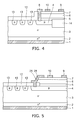
- FIG. 4 is a schematic view showing the principal cross-sectional structure of a semiconductor apparatus according to a third embodiment of the invention.
- an insulator 14 such as silicon oxide and silicon nitride is provided between the channel layer 6 and the n ⁇ -type silicon layer 3 below the drain electrode 9 .
- the voltage is also applied to the insulator 14 .
- the voltage is held by both the channel layer 6 and the insulator 14 .
- the channel layer 6 does not need to be so thickened for the purpose of ensuring adequate breakdown voltage. Because the channel layer 6 can be thinned, a crack-free AlGaN/GaN heterojunction structure of the barrier layer 7 and the channel layer 6 can be easily formed, and the substrate warpage can be also reduced.
- the structure shown in FIG. 4 can be realized by forming a groove extending from the surface of the p-type silicon layer 4 to the n ⁇ -type silicon layer 3 , filling the groove with an insulator 14 , and then forming an AlGaN/GaN heterojunction structure by selective growth.
- FIG. 5 is a schematic view showing the principal cross-sectional structure of a semiconductor apparatus according to a fourth embodiment of the invention.
- the field insulating film 12 is used as a mask to form a buffer layer 6 , a channel layer 6 , and a barrier layer 7 by selective epitaxial growth on the exposed surface of the p-type silicon layer 4 .
- the AlGaN/GaN heterojunction structure of the barrier layer 7 and the channel layer 6 is crystal grown like an island on the p-type silicon layer 4 . This allows the channel layer 6 to be thickened with good crystallinity as compared with the case of film-like crystal growth, and the breakdown voltage of the HFET can be increased.
- the source electrode 28 starts from the surface of the barrier layer 7 , passes through the facet 25 formed by selective island growth of the AlGaN/GaN heterojunction structure of the barrier layer 7 and the channel layer 6 , and extends onto the surface of the field insulating film 12 located at the level lower than the surface of the barrier layer 7 . That is, the source electrode 28 is integrally formed to cover the stepped portion formed from the surface of the barrier layer 7 , the facet 25 , and the surface of the field insulating film 12 . Furthermore, the source electrode 28 is connected to the p-type silicon layer 4 through a trench, which penetrates the field insulating film 12 below the source electrode 28 to the p-type silicon layer 4 .
- the structure of this embodiment allows integral formation of a source electrode 28 connected to both the barrier layer 7 and the p-type silicon layer 4 without forming a trench that starts from the surface of the barrier layer 7 , penetrates the underlying channel layer 6 and the buffer layer 5 , and reaches the p-type silicon layer 4 .
- the p-type silicon layer 4 is connected to the source electrode 28 , no voltage is applied to the sidewall (facet 25 ) of the AlGaN/GaN heterojunction structure of the barrier layer 7 and the channel layer 6 formed by island growth. Thus, leakage current can be avoided.
- a buffer layer 5 , a channel layer 6 , and a barrier layer 7 can be formed on the surface of the p-type silicon layer 4 at the bottom of the trench by selective epitaxial growth to prevent these growth layers from protruding outside the trench. This reduces irregularities on the device surface, facilitating the process for electrode formation.
- a trench extending from the surface of the barrier layer 7 to the p-type silicon layer 4 is formed to extract a source electrode 8 .
- the gap between the sidewall of the groove formed in the p-type silicon layer 4 and the nitride semiconductor layers (buffer layer 5 , channel layer 6 , and barrier layer 7 ) can be filled with a source electrode 38 .
- the nitride semiconductor layers can be electrically connected to the source electrode 38 at the facet 25 of the nitride semiconductor layers and the surface of the barrier layer 7 as in FIG.
- the p-type silicon layer 4 can be connected to the source electrode 38 at the sidewall of the trench formed in the p-type silicon layer 4 .
- the same effect as in the structure of FIG. 6 is achieved.
- the heterojunction structure of the barrier layer 7 and the channel layer 6 is described with reference to the combination of AlGaN/GaN.
- the present embodiments are also practicable using combinations such as GaN/InGaN, AlN/AlGaN, and AlN/GaN.
- the buffer layer 5 is not limited to undoped AlGaN, but can be made of n-type AlGaN. Alternatively, other nitride semiconductors such as a laminated structure of AlN/GaN can be used as a buffer layer.
- the gate structure of the HFET is described as a gate structure based on the Schottky junction.
- the present embodiments are also practicable using an insulated gate structure in which a gate insulating film 15 is provided between the barrier layer 7 and the gate electrode 10 .
- the gallium nitride-based HFET is typically implemented as a normally-on device having a negative gate threshold voltage.
- a p-type layer 16 can be provided in the heterojunction structure of the barrier layer 7 and the channel layer 6 below the gate electrode 10 to eliminate two-dimensional electron gas below the gate electrode 10 in the off-state, thereby realizing a normally-off device.
- the normally-off operation can be also realized by using other structures to shift the threshold voltage to the positive side, such as a structure in which a p-type GaN layer is crystal grown as a channel layer, or a recessed gate structure.
- a field plate structure in which a field plate electrode 17 connected to the source electrode 8 is provided via a field insulating film 19 .
- the gate-drain structure of the HFET is similar to a heterojunction Schottky barrier diode (HSBD).
- HSBD heterojunction Schottky barrier diode
- the second silicon layer 3 is not limited to having a fixed impurity concentration.
- the concentration can be varied so that it is high near the first silicon layer 2 , and low near the third silicon layer 4 .
- the concentration can be varied either gradually or stepwise.
Landscapes
- Junction Field-Effect Transistors (AREA)
- Semiconductor Integrated Circuits (AREA)
- Metal-Oxide And Bipolar Metal-Oxide Semiconductor Integrated Circuits (AREA)
Abstract
Description
Claims (17)
Applications Claiming Priority (2)
| Application Number | Priority Date | Filing Date | Title |
|---|---|---|---|
| JP2007167427A JP4478175B2 (en) | 2007-06-26 | 2007-06-26 | Semiconductor device |
| JP2007-167427 | 2007-06-26 |
Publications (2)
| Publication Number | Publication Date |
|---|---|
| US20090008679A1 US20090008679A1 (en) | 2009-01-08 |
| US7884395B2 true US7884395B2 (en) | 2011-02-08 |
Family
ID=40220752
Family Applications (1)
| Application Number | Title | Priority Date | Filing Date |
|---|---|---|---|
| US12/145,980 Expired - Fee Related US7884395B2 (en) | 2007-06-26 | 2008-06-25 | Semiconductor apparatus |
Country Status (2)
| Country | Link |
|---|---|
| US (1) | US7884395B2 (en) |
| JP (1) | JP4478175B2 (en) |
Cited By (50)
| Publication number | Priority date | Publication date | Assignee | Title |
|---|---|---|---|---|
| US20090072269A1 (en) * | 2007-09-17 | 2009-03-19 | Chang Soo Suh | Gallium nitride diodes and integrated components |
| US20100140876A1 (en) * | 2008-12-04 | 2010-06-10 | Schlumberger Technology Corporation | Sealing gland and methods of use |
| US20100163928A1 (en) * | 2008-12-26 | 2010-07-01 | Fujitsu Limited | Compound semiconductor device and manufacturing method of the same |
| US20100289067A1 (en) * | 2009-05-14 | 2010-11-18 | Transphorm Inc. | High Voltage III-Nitride Semiconductor Devices |
| US20100311230A1 (en) * | 2008-07-31 | 2010-12-09 | Mitsubishi Electric Corporation | Semiconductor device and method of fabricating the same |
| US20110049526A1 (en) * | 2009-08-28 | 2011-03-03 | Transphorm Inc. | Semiconductor Devices with Field Plates |
| US20110127541A1 (en) * | 2008-12-10 | 2011-06-02 | Transphorm Inc. | Semiconductor heterostructure diodes |
| US20110140172A1 (en) * | 2009-12-10 | 2011-06-16 | Transphorm Inc. | Reverse side engineered iii-nitride devices |
| US20130015498A1 (en) * | 2011-07-15 | 2013-01-17 | International Rectifier Corporation (El Segundo, Ca) | Composite Semiconductor Device with Integrated Diode |
| US8519438B2 (en) | 2008-04-23 | 2013-08-27 | Transphorm Inc. | Enhancement mode III-N HEMTs |
| US8581301B2 (en) | 2012-03-23 | 2013-11-12 | Kabushiki Kaisha Toshiba | Nitride semiconductor device |
| US8598937B2 (en) | 2011-10-07 | 2013-12-03 | Transphorm Inc. | High power semiconductor electronic components with increased reliability |
| US8643062B2 (en) | 2011-02-02 | 2014-02-04 | Transphorm Inc. | III-N device structures and methods |
| US8716141B2 (en) | 2011-03-04 | 2014-05-06 | Transphorm Inc. | Electrode configurations for semiconductor devices |
| US8742460B2 (en) | 2010-12-15 | 2014-06-03 | Transphorm Inc. | Transistors with isolation regions |
| US8772842B2 (en) | 2011-03-04 | 2014-07-08 | Transphorm, Inc. | Semiconductor diodes with low reverse bias currents |
| US8816751B2 (en) | 2008-09-23 | 2014-08-26 | Transphorm Inc. | Inductive load power switching circuits |
| US8901604B2 (en) | 2011-09-06 | 2014-12-02 | Transphorm Inc. | Semiconductor devices with guard rings |
| US8912839B2 (en) | 2008-02-12 | 2014-12-16 | Transphorm Inc. | Bridge circuits and their components |
| US20150108547A1 (en) * | 2013-10-17 | 2015-04-23 | Samsung Electronics Co., Ltd. | High electron mobility transistor |
| US9059076B2 (en) | 2013-04-01 | 2015-06-16 | Transphorm Inc. | Gate drivers for circuits based on semiconductor devices |
| US9093366B2 (en) | 2012-04-09 | 2015-07-28 | Transphorm Inc. | N-polar III-nitride transistors |
| US9123635B2 (en) | 2012-12-14 | 2015-09-01 | Toyoda Gosei Co., Ltd. | Manufacturing method of semiconductor device |
| US9165766B2 (en) | 2012-02-03 | 2015-10-20 | Transphorm Inc. | Buffer layer structures suited for III-nitride devices with foreign substrates |
| US9171730B2 (en) | 2013-02-15 | 2015-10-27 | Transphorm Inc. | Electrodes for semiconductor devices and methods of forming the same |
| US9184275B2 (en) | 2012-06-27 | 2015-11-10 | Transphorm Inc. | Semiconductor devices with integrated hole collectors |
| US9190295B2 (en) | 2009-11-02 | 2015-11-17 | Transphorm Inc. | Package configurations for low EMI circuits |
| US9224721B2 (en) | 2012-02-24 | 2015-12-29 | Transphorm Inc. | Semiconductor power modules and devices |
| US9245992B2 (en) | 2013-03-15 | 2016-01-26 | Transphorm Inc. | Carbon doping semiconductor devices |
| US9281388B2 (en) | 2011-07-15 | 2016-03-08 | Infineon Technologies Americas Corp. | Composite semiconductor device with a SOI substrate having an integrated diode |
| US9306051B2 (en) | 2014-02-06 | 2016-04-05 | Renesas Electronics Corporation | Semiconductor device using a nitride semiconductor |
| US9318593B2 (en) | 2014-07-21 | 2016-04-19 | Transphorm Inc. | Forming enhancement mode III-nitride devices |
| US9331157B2 (en) | 2012-12-14 | 2016-05-03 | Toyoda Gosei Co., Ltd. | Semiconductor device |
| US9391150B2 (en) | 2012-12-14 | 2016-07-12 | Toyoda Gosei Co., Ltd. | Semiconductor Device |
| US9443950B2 (en) | 2012-12-14 | 2016-09-13 | Toyoda Gosei Co., Ltd. | Semiconductor device |
| US9443938B2 (en) | 2013-07-19 | 2016-09-13 | Transphorm Inc. | III-nitride transistor including a p-type depleting layer |
| US9520489B2 (en) | 2014-02-05 | 2016-12-13 | Renesas Electronics Corporation | Semiconductor device |
| US9536967B2 (en) | 2014-12-16 | 2017-01-03 | Transphorm Inc. | Recessed ohmic contacts in a III-N device |
| US9537425B2 (en) | 2013-07-09 | 2017-01-03 | Transphorm Inc. | Multilevel inverters and their components |
| US9536966B2 (en) | 2014-12-16 | 2017-01-03 | Transphorm Inc. | Gate structures for III-N devices |
| US9543940B2 (en) | 2014-07-03 | 2017-01-10 | Transphorm Inc. | Switching circuits having ferrite beads |
| US9590494B1 (en) | 2014-07-17 | 2017-03-07 | Transphorm Inc. | Bridgeless power factor correction circuits |
| US9589951B2 (en) | 2014-08-20 | 2017-03-07 | Renesas Electronics Corporation | High-electron-mobility transistor with protective diode |
| US9590060B2 (en) | 2013-03-13 | 2017-03-07 | Transphorm Inc. | Enhancement-mode III-nitride devices |
| US9997507B2 (en) | 2013-07-25 | 2018-06-12 | General Electric Company | Semiconductor assembly and method of manufacture |
| US10200030B2 (en) | 2015-03-13 | 2019-02-05 | Transphorm Inc. | Paralleling of switching devices for high power circuits |
| US10224401B2 (en) | 2016-05-31 | 2019-03-05 | Transphorm Inc. | III-nitride devices including a graded depleting layer |
| US10319648B2 (en) | 2017-04-17 | 2019-06-11 | Transphorm Inc. | Conditions for burn-in of high power semiconductors |
| US11322599B2 (en) | 2016-01-15 | 2022-05-03 | Transphorm Technology, Inc. | Enhancement mode III-nitride devices having an Al1-xSixO gate insulator |
| US11476325B2 (en) * | 2018-06-30 | 2022-10-18 | Jin WEI | Semiconductor device |
Families Citing this family (24)
| Publication number | Priority date | Publication date | Assignee | Title |
|---|---|---|---|---|
| JP5384029B2 (en) * | 2007-08-23 | 2014-01-08 | 日本碍子株式会社 | MIS gate structure type HEMT device and method for manufacturing MIS gate structure type HEMT device |
| JPWO2010001607A1 (en) * | 2008-07-03 | 2011-12-15 | パナソニック株式会社 | Nitride semiconductor device |
| JP5524462B2 (en) * | 2008-08-06 | 2014-06-18 | シャープ株式会社 | Semiconductor device |
| US20100207164A1 (en) * | 2008-08-22 | 2010-08-19 | Daisuke Shibata | Field effect transistor |
| DE102009018054B4 (en) * | 2009-04-21 | 2018-11-29 | Infineon Technologies Austria Ag | Lateral HEMT and method of making a lateral HEMT |
| KR20130126948A (en) | 2010-12-15 | 2013-11-21 | 이피션트 파워 컨버젼 코퍼레이션 | Semiconductor devices with back surface isolation |
| JP5758132B2 (en) * | 2011-01-26 | 2015-08-05 | 株式会社東芝 | Semiconductor element |
| US20120256190A1 (en) * | 2011-04-11 | 2012-10-11 | International Rectifier Corporation | Stacked Composite Device Including a Group III-V Transistor and a Group IV Diode |
| US9343440B2 (en) | 2011-04-11 | 2016-05-17 | Infineon Technologies Americas Corp. | Stacked composite device including a group III-V transistor and a group IV vertical transistor |
| EP2639832A3 (en) * | 2012-03-15 | 2015-08-05 | International Rectifier Corporation | Group III-V and group IV composite diode |
| US9362267B2 (en) | 2012-03-15 | 2016-06-07 | Infineon Technologies Americas Corp. | Group III-V and group IV composite switch |
| JP6211804B2 (en) * | 2013-05-30 | 2017-10-11 | トランスフォーム・ジャパン株式会社 | Semiconductor device |
| JP6135487B2 (en) * | 2013-12-09 | 2017-05-31 | 富士通株式会社 | Semiconductor device and manufacturing method of semiconductor device |
| JP2015177016A (en) * | 2014-03-14 | 2015-10-05 | 株式会社東芝 | semiconductor device |
| JP2017157589A (en) * | 2016-02-29 | 2017-09-07 | ルネサスエレクトロニクス株式会社 | Semiconductor device and semiconductor device manufacturing method |
| DE102017103111B4 (en) * | 2017-02-16 | 2025-03-13 | Semikron Elektronik Gmbh & Co. Kg | Semiconductor diode and electronic circuit arrangement herewith |
| US10804369B2 (en) | 2017-04-28 | 2020-10-13 | Mitsubishi Electric Corporation | Semiconductor device |
| TWI695418B (en) * | 2017-09-22 | 2020-06-01 | 新唐科技股份有限公司 | Semiconductor device and method of manufacturing the same |
| CN109037325B (en) * | 2018-06-22 | 2021-06-15 | 杭州电子科技大学 | A GaN field effect transistor with electrodes connected to a PIN buried tube |
| US10840798B1 (en) | 2018-09-28 | 2020-11-17 | Dialog Semiconductor (Uk) Limited | Bidirectional signaling method for high-voltage floating circuits |
| CN112466927B (en) * | 2020-11-26 | 2021-11-02 | 东南大学 | A heterojunction semiconductor device with avalanche impact resistance |
| US12261168B2 (en) * | 2021-02-16 | 2025-03-25 | Efficient Power Conversion Corporation | Gate metal-insulator-field plate metal integrated circuit capacitor and method of forming the same |
| US20240395805A1 (en) * | 2023-05-26 | 2024-11-28 | Cambridge Gan Devices Limited | Power semiconductor device comprising a silicon substrate |
| IT202300015852A1 (en) * | 2023-07-27 | 2025-01-27 | St Microelectronics Int Nv | SEMICONDUCTOR ELECTRONIC DEVICE COMPRISING A HETEROSTRUCTURE-BASED ELECTRONIC COMPONENT AND MANUFACTURING PROCEDURE |
Citations (14)
| Publication number | Priority date | Publication date | Assignee | Title |
|---|---|---|---|---|
| US4200877A (en) * | 1976-12-23 | 1980-04-29 | Hitachi, Ltd. | Temperature-compensated voltage reference diode with intermediate polycrystalline layer |
| JP2001168111A (en) | 1999-12-07 | 2001-06-22 | Nippon Telegr & Teleph Corp <Ntt> | GaN field effect transistor |
| JP2003229566A (en) | 2001-11-27 | 2003-08-15 | Furukawa Electric Co Ltd:The | Power conversion device and GaN-based semiconductor device used therefor |
| US20040124500A1 (en) * | 2001-04-12 | 2004-07-01 | Kimihiro Kawagoe | Gallium nitride compound semiconductor element |
| US20050062069A1 (en) | 2003-09-19 | 2005-03-24 | Wataru Saito | Power semiconductor device |
| US20050189559A1 (en) * | 2004-02-27 | 2005-09-01 | Kabushiki Kaisha Toshiba | Semiconductor device |
| JP2007059589A (en) | 2005-08-24 | 2007-03-08 | Toshiba Corp | Nitride semiconductor device |
| US20070051977A1 (en) | 2005-08-24 | 2007-03-08 | Kabushiki Kaisha Toshiba | Nitride semiconductor device |
| US7199408B2 (en) * | 2004-06-15 | 2007-04-03 | Ngk Insulators, Ltd. | Semiconductor multilayer structure, semiconductor device and HEMT device |
| US20070170463A1 (en) * | 2006-01-25 | 2007-07-26 | Hiroaki Ueno | Nitride semiconductor device |
| US7250641B2 (en) | 2004-06-15 | 2007-07-31 | Kabushiki Kaisha Toshiba | Nitride semiconductor device |
| US7271429B2 (en) | 2004-09-02 | 2007-09-18 | Kabushiki Kaisha Toshiba | Nitride semiconductor device |
| US7329909B2 (en) | 2005-02-02 | 2008-02-12 | Kabushiki Kaisha Toshiba | Nitride semiconductor device |
| JP2009004398A (en) | 2007-06-19 | 2009-01-08 | Renesas Technology Corp | Semiconductor device and power conversion device using the same |
-
2007
- 2007-06-26 JP JP2007167427A patent/JP4478175B2/en not_active Expired - Fee Related
-
2008
- 2008-06-25 US US12/145,980 patent/US7884395B2/en not_active Expired - Fee Related
Patent Citations (15)
| Publication number | Priority date | Publication date | Assignee | Title |
|---|---|---|---|---|
| US4200877A (en) * | 1976-12-23 | 1980-04-29 | Hitachi, Ltd. | Temperature-compensated voltage reference diode with intermediate polycrystalline layer |
| JP2001168111A (en) | 1999-12-07 | 2001-06-22 | Nippon Telegr & Teleph Corp <Ntt> | GaN field effect transistor |
| US20040124500A1 (en) * | 2001-04-12 | 2004-07-01 | Kimihiro Kawagoe | Gallium nitride compound semiconductor element |
| JP2003229566A (en) | 2001-11-27 | 2003-08-15 | Furukawa Electric Co Ltd:The | Power conversion device and GaN-based semiconductor device used therefor |
| US20050062069A1 (en) | 2003-09-19 | 2005-03-24 | Wataru Saito | Power semiconductor device |
| US20050189559A1 (en) * | 2004-02-27 | 2005-09-01 | Kabushiki Kaisha Toshiba | Semiconductor device |
| US7250641B2 (en) | 2004-06-15 | 2007-07-31 | Kabushiki Kaisha Toshiba | Nitride semiconductor device |
| US7199408B2 (en) * | 2004-06-15 | 2007-04-03 | Ngk Insulators, Ltd. | Semiconductor multilayer structure, semiconductor device and HEMT device |
| US7271429B2 (en) | 2004-09-02 | 2007-09-18 | Kabushiki Kaisha Toshiba | Nitride semiconductor device |
| US7329909B2 (en) | 2005-02-02 | 2008-02-12 | Kabushiki Kaisha Toshiba | Nitride semiconductor device |
| JP2007059589A (en) | 2005-08-24 | 2007-03-08 | Toshiba Corp | Nitride semiconductor device |
| US20070200143A1 (en) | 2005-08-24 | 2007-08-30 | Kabushiki Kaisha Toshiba | Nitride semiconductor device |
| US20070051977A1 (en) | 2005-08-24 | 2007-03-08 | Kabushiki Kaisha Toshiba | Nitride semiconductor device |
| US20070170463A1 (en) * | 2006-01-25 | 2007-07-26 | Hiroaki Ueno | Nitride semiconductor device |
| JP2009004398A (en) | 2007-06-19 | 2009-01-08 | Renesas Technology Corp | Semiconductor device and power conversion device using the same |
Cited By (107)
| Publication number | Priority date | Publication date | Assignee | Title |
|---|---|---|---|---|
| US20090072269A1 (en) * | 2007-09-17 | 2009-03-19 | Chang Soo Suh | Gallium nitride diodes and integrated components |
| US8912839B2 (en) | 2008-02-12 | 2014-12-16 | Transphorm Inc. | Bridge circuits and their components |
| US9899998B2 (en) | 2008-02-12 | 2018-02-20 | Transphorm Inc. | Bridge circuits and their components |
| US9437708B2 (en) | 2008-04-23 | 2016-09-06 | Transphorm Inc. | Enhancement mode III-N HEMTs |
| US8841702B2 (en) | 2008-04-23 | 2014-09-23 | Transphorm Inc. | Enhancement mode III-N HEMTs |
| US9941399B2 (en) | 2008-04-23 | 2018-04-10 | Transphorm Inc. | Enhancement mode III-N HEMTs |
| US9196716B2 (en) | 2008-04-23 | 2015-11-24 | Transphorm Inc. | Enhancement mode III-N HEMTs |
| US8519438B2 (en) | 2008-04-23 | 2013-08-27 | Transphorm Inc. | Enhancement mode III-N HEMTs |
| US20100311230A1 (en) * | 2008-07-31 | 2010-12-09 | Mitsubishi Electric Corporation | Semiconductor device and method of fabricating the same |
| US8420496B2 (en) * | 2008-07-31 | 2013-04-16 | Mitsubishi Electric Corporation | Semiconductor device and method of fabricating the same |
| US9690314B2 (en) | 2008-09-23 | 2017-06-27 | Transphorm Inc. | Inductive load power switching circuits |
| US8816751B2 (en) | 2008-09-23 | 2014-08-26 | Transphorm Inc. | Inductive load power switching circuits |
| US20100140876A1 (en) * | 2008-12-04 | 2010-06-10 | Schlumberger Technology Corporation | Sealing gland and methods of use |
| US8376366B2 (en) * | 2008-12-04 | 2013-02-19 | Schlumberger Technology Corporation | Sealing gland and methods of use |
| US20120267640A1 (en) * | 2008-12-10 | 2012-10-25 | Transphorm Inc. | Semiconductor heterostructure diodes |
| US8237198B2 (en) * | 2008-12-10 | 2012-08-07 | Transphorm Inc. | Semiconductor heterostructure diodes |
| US9041065B2 (en) * | 2008-12-10 | 2015-05-26 | Transphorm Inc. | Semiconductor heterostructure diodes |
| US20110127541A1 (en) * | 2008-12-10 | 2011-06-02 | Transphorm Inc. | Semiconductor heterostructure diodes |
| US8541818B2 (en) * | 2008-12-10 | 2013-09-24 | Transphorm Inc. | Semiconductor heterostructure diodes |
| US20140054603A1 (en) * | 2008-12-10 | 2014-02-27 | Transphorm Inc. | Semiconductor Heterostructure Diodes |
| US8198653B2 (en) * | 2008-12-26 | 2012-06-12 | Fujitsu Limited | Compound semiconductor device and manufacturing method of the same |
| US20100163928A1 (en) * | 2008-12-26 | 2010-07-01 | Fujitsu Limited | Compound semiconductor device and manufacturing method of the same |
| US20120139008A1 (en) * | 2008-12-26 | 2012-06-07 | Fujitsu Limited | Compound semiconductor device and manufacturing method of the same |
| US8735942B2 (en) * | 2008-12-26 | 2014-05-27 | Fujitsu Limited | Compound semiconductor device and manufacturing method of the same |
| US20100289067A1 (en) * | 2009-05-14 | 2010-11-18 | Transphorm Inc. | High Voltage III-Nitride Semiconductor Devices |
| US9293561B2 (en) | 2009-05-14 | 2016-03-22 | Transphorm Inc. | High voltage III-nitride semiconductor devices |
| US8742459B2 (en) | 2009-05-14 | 2014-06-03 | Transphorm Inc. | High voltage III-nitride semiconductor devices |
| US20110049526A1 (en) * | 2009-08-28 | 2011-03-03 | Transphorm Inc. | Semiconductor Devices with Field Plates |
| US9831315B2 (en) | 2009-08-28 | 2017-11-28 | Transphorm Inc. | Semiconductor devices with field plates |
| US8692294B2 (en) | 2009-08-28 | 2014-04-08 | Transphorm Inc. | Semiconductor devices with field plates |
| US8390000B2 (en) | 2009-08-28 | 2013-03-05 | Transphorm Inc. | Semiconductor devices with field plates |
| US9111961B2 (en) | 2009-08-28 | 2015-08-18 | Transphorm Inc. | Semiconductor devices with field plates |
| US9373699B2 (en) | 2009-08-28 | 2016-06-21 | Transphorm Inc. | Semiconductor devices with field plates |
| US9190295B2 (en) | 2009-11-02 | 2015-11-17 | Transphorm Inc. | Package configurations for low EMI circuits |
| US20110140172A1 (en) * | 2009-12-10 | 2011-06-16 | Transphorm Inc. | Reverse side engineered iii-nitride devices |
| US10199217B2 (en) | 2009-12-10 | 2019-02-05 | Transphorm Inc. | Methods of forming reverse side engineered III-nitride devices |
| US9496137B2 (en) | 2009-12-10 | 2016-11-15 | Transphorm Inc. | Methods of forming reverse side engineered III-nitride devices |
| US8389977B2 (en) | 2009-12-10 | 2013-03-05 | Transphorm Inc. | Reverse side engineered III-nitride devices |
| US8742460B2 (en) | 2010-12-15 | 2014-06-03 | Transphorm Inc. | Transistors with isolation regions |
| US9437707B2 (en) | 2010-12-15 | 2016-09-06 | Transphorm Inc. | Transistors with isolation regions |
| US9147760B2 (en) | 2010-12-15 | 2015-09-29 | Transphorm Inc. | Transistors with isolation regions |
| US8895421B2 (en) | 2011-02-02 | 2014-11-25 | Transphorm Inc. | III-N device structures and methods |
| US8643062B2 (en) | 2011-02-02 | 2014-02-04 | Transphorm Inc. | III-N device structures and methods |
| US9224671B2 (en) | 2011-02-02 | 2015-12-29 | Transphorm Inc. | III-N device structures and methods |
| US8716141B2 (en) | 2011-03-04 | 2014-05-06 | Transphorm Inc. | Electrode configurations for semiconductor devices |
| US9142659B2 (en) | 2011-03-04 | 2015-09-22 | Transphorm Inc. | Electrode configurations for semiconductor devices |
| US8895423B2 (en) | 2011-03-04 | 2014-11-25 | Transphorm Inc. | Method for making semiconductor diodes with low reverse bias currents |
| US8772842B2 (en) | 2011-03-04 | 2014-07-08 | Transphorm, Inc. | Semiconductor diodes with low reverse bias currents |
| US9087812B2 (en) * | 2011-07-15 | 2015-07-21 | International Rectifier Corporation | Composite semiconductor device with integrated diode |
| US9281388B2 (en) | 2011-07-15 | 2016-03-08 | Infineon Technologies Americas Corp. | Composite semiconductor device with a SOI substrate having an integrated diode |
| US20130015498A1 (en) * | 2011-07-15 | 2013-01-17 | International Rectifier Corporation (El Segundo, Ca) | Composite Semiconductor Device with Integrated Diode |
| US9224805B2 (en) | 2011-09-06 | 2015-12-29 | Transphorm Inc. | Semiconductor devices with guard rings |
| US8901604B2 (en) | 2011-09-06 | 2014-12-02 | Transphorm Inc. | Semiconductor devices with guard rings |
| US9171836B2 (en) | 2011-10-07 | 2015-10-27 | Transphorm Inc. | Method of forming electronic components with increased reliability |
| US8598937B2 (en) | 2011-10-07 | 2013-12-03 | Transphorm Inc. | High power semiconductor electronic components with increased reliability |
| US8860495B2 (en) | 2011-10-07 | 2014-10-14 | Transphorm Inc. | Method of forming electronic components with increased reliability |
| US9685323B2 (en) | 2012-02-03 | 2017-06-20 | Transphorm Inc. | Buffer layer structures suited for III-nitride devices with foreign substrates |
| US9165766B2 (en) | 2012-02-03 | 2015-10-20 | Transphorm Inc. | Buffer layer structures suited for III-nitride devices with foreign substrates |
| US9741702B2 (en) | 2012-02-24 | 2017-08-22 | Transphorm Inc. | Semiconductor power modules and devices |
| US9224721B2 (en) | 2012-02-24 | 2015-12-29 | Transphorm Inc. | Semiconductor power modules and devices |
| US8581301B2 (en) | 2012-03-23 | 2013-11-12 | Kabushiki Kaisha Toshiba | Nitride semiconductor device |
| US8928039B2 (en) | 2012-03-23 | 2015-01-06 | Kabushiki Kaisha Toshiba | Semiconductor device including heterojunction field effect transistor and Schottky barrier diode |
| US9093366B2 (en) | 2012-04-09 | 2015-07-28 | Transphorm Inc. | N-polar III-nitride transistors |
| US9490324B2 (en) | 2012-04-09 | 2016-11-08 | Transphorm Inc. | N-polar III-nitride transistors |
| US9634100B2 (en) | 2012-06-27 | 2017-04-25 | Transphorm Inc. | Semiconductor devices with integrated hole collectors |
| US9184275B2 (en) | 2012-06-27 | 2015-11-10 | Transphorm Inc. | Semiconductor devices with integrated hole collectors |
| US9123635B2 (en) | 2012-12-14 | 2015-09-01 | Toyoda Gosei Co., Ltd. | Manufacturing method of semiconductor device |
| US9391150B2 (en) | 2012-12-14 | 2016-07-12 | Toyoda Gosei Co., Ltd. | Semiconductor Device |
| US9443950B2 (en) | 2012-12-14 | 2016-09-13 | Toyoda Gosei Co., Ltd. | Semiconductor device |
| US9331157B2 (en) | 2012-12-14 | 2016-05-03 | Toyoda Gosei Co., Ltd. | Semiconductor device |
| US9520491B2 (en) | 2013-02-15 | 2016-12-13 | Transphorm Inc. | Electrodes for semiconductor devices and methods of forming the same |
| US9171730B2 (en) | 2013-02-15 | 2015-10-27 | Transphorm Inc. | Electrodes for semiconductor devices and methods of forming the same |
| US9590060B2 (en) | 2013-03-13 | 2017-03-07 | Transphorm Inc. | Enhancement-mode III-nitride devices |
| US10535763B2 (en) | 2013-03-13 | 2020-01-14 | Transphorm Inc. | Enhancement-mode III-nitride devices |
| US10043898B2 (en) | 2013-03-13 | 2018-08-07 | Transphorm Inc. | Enhancement-mode III-nitride devices |
| US9865719B2 (en) | 2013-03-15 | 2018-01-09 | Transphorm Inc. | Carbon doping semiconductor devices |
| US9245993B2 (en) | 2013-03-15 | 2016-01-26 | Transphorm Inc. | Carbon doping semiconductor devices |
| US9245992B2 (en) | 2013-03-15 | 2016-01-26 | Transphorm Inc. | Carbon doping semiconductor devices |
| US9059076B2 (en) | 2013-04-01 | 2015-06-16 | Transphorm Inc. | Gate drivers for circuits based on semiconductor devices |
| US9362903B2 (en) | 2013-04-01 | 2016-06-07 | Transphorm Inc. | Gate drivers for circuits based on semiconductor devices |
| US9537425B2 (en) | 2013-07-09 | 2017-01-03 | Transphorm Inc. | Multilevel inverters and their components |
| US10043896B2 (en) | 2013-07-19 | 2018-08-07 | Transphorm Inc. | III-Nitride transistor including a III-N depleting layer |
| US9842922B2 (en) | 2013-07-19 | 2017-12-12 | Transphorm Inc. | III-nitride transistor including a p-type depleting layer |
| US9443938B2 (en) | 2013-07-19 | 2016-09-13 | Transphorm Inc. | III-nitride transistor including a p-type depleting layer |
| US9997507B2 (en) | 2013-07-25 | 2018-06-12 | General Electric Company | Semiconductor assembly and method of manufacture |
| US9252253B2 (en) * | 2013-10-17 | 2016-02-02 | Samsung Electronics Co., Ltd. | High electron mobility transistor |
| US20150108547A1 (en) * | 2013-10-17 | 2015-04-23 | Samsung Electronics Co., Ltd. | High electron mobility transistor |
| US9837519B2 (en) | 2014-02-05 | 2017-12-05 | Renesas Electronics Corporation | Semiconductor device |
| US9520489B2 (en) | 2014-02-05 | 2016-12-13 | Renesas Electronics Corporation | Semiconductor device |
| US9306051B2 (en) | 2014-02-06 | 2016-04-05 | Renesas Electronics Corporation | Semiconductor device using a nitride semiconductor |
| US9543940B2 (en) | 2014-07-03 | 2017-01-10 | Transphorm Inc. | Switching circuits having ferrite beads |
| US9991884B2 (en) | 2014-07-03 | 2018-06-05 | Transphorm Inc. | Switching circuits having ferrite beads |
| US9660640B2 (en) | 2014-07-03 | 2017-05-23 | Transphorm Inc. | Switching circuits having ferrite beads |
| US9590494B1 (en) | 2014-07-17 | 2017-03-07 | Transphorm Inc. | Bridgeless power factor correction circuits |
| US10063138B1 (en) | 2014-07-17 | 2018-08-28 | Transphorm Inc. | Bridgeless power factor correction circuits |
| US9318593B2 (en) | 2014-07-21 | 2016-04-19 | Transphorm Inc. | Forming enhancement mode III-nitride devices |
| US9935190B2 (en) | 2014-07-21 | 2018-04-03 | Transphorm Inc. | Forming enhancement mode III-nitride devices |
| US9589951B2 (en) | 2014-08-20 | 2017-03-07 | Renesas Electronics Corporation | High-electron-mobility transistor with protective diode |
| US9536967B2 (en) | 2014-12-16 | 2017-01-03 | Transphorm Inc. | Recessed ohmic contacts in a III-N device |
| US9536966B2 (en) | 2014-12-16 | 2017-01-03 | Transphorm Inc. | Gate structures for III-N devices |
| US10200030B2 (en) | 2015-03-13 | 2019-02-05 | Transphorm Inc. | Paralleling of switching devices for high power circuits |
| US11322599B2 (en) | 2016-01-15 | 2022-05-03 | Transphorm Technology, Inc. | Enhancement mode III-nitride devices having an Al1-xSixO gate insulator |
| US10224401B2 (en) | 2016-05-31 | 2019-03-05 | Transphorm Inc. | III-nitride devices including a graded depleting layer |
| US10629681B2 (en) | 2016-05-31 | 2020-04-21 | Transphorm Technology, Inc. | III-nitride devices including a graded depleting layer |
| US11121216B2 (en) | 2016-05-31 | 2021-09-14 | Transphorm Technology, Inc. | III-nitride devices including a graded depleting layer |
| US10319648B2 (en) | 2017-04-17 | 2019-06-11 | Transphorm Inc. | Conditions for burn-in of high power semiconductors |
| US11476325B2 (en) * | 2018-06-30 | 2022-10-18 | Jin WEI | Semiconductor device |
Also Published As
| Publication number | Publication date |
|---|---|
| JP2009009993A (en) | 2009-01-15 |
| US20090008679A1 (en) | 2009-01-08 |
| JP4478175B2 (en) | 2010-06-09 |
Similar Documents
| Publication | Publication Date | Title |
|---|---|---|
| US7884395B2 (en) | Semiconductor apparatus | |
| US8552471B2 (en) | Semiconductor apparatus having reverse blocking characteristics and method of manufacturing the same | |
| US7508015B2 (en) | Semiconductor device using a nitride semiconductor | |
| US9029915B2 (en) | Nitride semiconductor device | |
| US8519439B2 (en) | Nitride semiconductor element with N-face semiconductor crystal layer | |
| US7250641B2 (en) | Nitride semiconductor device | |
| US6933544B2 (en) | Power semiconductor device | |
| US8981380B2 (en) | Monolithic integration of silicon and group III-V devices | |
| US9589951B2 (en) | High-electron-mobility transistor with protective diode | |
| EP3539159B1 (en) | Semiconductor devices with multiple channels and three-dimensional electrodes | |
| KR101636134B1 (en) | Semiconductor device | |
| KR20160057343A (en) | A STRUCTURE FOR A GALLIUM NITRIDE (GaN) HIGH ELECTRON MOBILITY TRANSISTOR | |
| KR20140042470A (en) | Normally off high electron mobility transistor | |
| US9231056B2 (en) | Semiconductor device and fabrication method therefor, and power supply apparatus | |
| WO2011024367A1 (en) | Nitride semiconductor device | |
| US11211481B2 (en) | III-V semiconductor device | |
| US20230387286A1 (en) | Nitride semiconductor device | |
| JP2011029507A (en) | Semiconductor device | |
| TWI732813B (en) | Semiconductor device, electronic part, electronic apparatus, and method for fabricating semiconductor device | |
| US8969926B2 (en) | Vertical GaN JFET with low gate-drain capacitance and high gate-source capacitance | |
| JP2008016588A (en) | GaN-based semiconductor devices | |
| JP5549081B2 (en) | Semiconductor device and manufacturing method thereof | |
| JP5545653B2 (en) | Nitride semiconductor device | |
| US20240313061A1 (en) | Nitride semiconductor device | |
| JP2013183034A (en) | Power semiconductor device |
Legal Events
| Date | Code | Title | Description |
|---|---|---|---|
| AS | Assignment |
Owner name: KABUSHIKI KAISHA TOSHIBA, JAPAN Free format text: ASSIGNMENT OF ASSIGNORS INTEREST;ASSIGNOR:SAITO, WATARU;REEL/FRAME:021584/0973 Effective date: 20080722 |
|
| FEPP | Fee payment procedure |
Free format text: PAYOR NUMBER ASSIGNED (ORIGINAL EVENT CODE: ASPN); ENTITY STATUS OF PATENT OWNER: LARGE ENTITY |
|
| FPAY | Fee payment |
Year of fee payment: 4 |
|
| FEPP | Fee payment procedure |
Free format text: MAINTENANCE FEE REMINDER MAILED (ORIGINAL EVENT CODE: REM.); ENTITY STATUS OF PATENT OWNER: LARGE ENTITY |
|
| LAPS | Lapse for failure to pay maintenance fees |
Free format text: PATENT EXPIRED FOR FAILURE TO PAY MAINTENANCE FEES (ORIGINAL EVENT CODE: EXP.); ENTITY STATUS OF PATENT OWNER: LARGE ENTITY |
|
| STCH | Information on status: patent discontinuation |
Free format text: PATENT EXPIRED DUE TO NONPAYMENT OF MAINTENANCE FEES UNDER 37 CFR 1.362 |
|
| FP | Lapsed due to failure to pay maintenance fee |
Effective date: 20190208 |