WO2014203948A1 - 積層セラミックコンデンサ - Google Patents
積層セラミックコンデンサ Download PDFInfo
- Publication number
- WO2014203948A1 WO2014203948A1 PCT/JP2014/066223 JP2014066223W WO2014203948A1 WO 2014203948 A1 WO2014203948 A1 WO 2014203948A1 JP 2014066223 W JP2014066223 W JP 2014066223W WO 2014203948 A1 WO2014203948 A1 WO 2014203948A1
- Authority
- WO
- WIPO (PCT)
- Prior art keywords
- thickness
- capacitor
- height
- multilayer ceramic
- width
- Prior art date
- Legal status (The legal status is an assumption and is not a legal conclusion. Google has not performed a legal analysis and makes no representation as to the accuracy of the status listed.)
- Ceased
Links
Images




Classifications
-
- H—ELECTRICITY
- H01—ELECTRIC ELEMENTS
- H01G—CAPACITORS; CAPACITORS, RECTIFIERS, DETECTORS, SWITCHING DEVICES, LIGHT-SENSITIVE OR TEMPERATURE-SENSITIVE DEVICES OF THE ELECTROLYTIC TYPE
- H01G4/00—Fixed capacitors; Processes of their manufacture
- H01G4/002—Details
- H01G4/005—Electrodes
- H01G4/012—Form of non-self-supporting electrodes
-
- H—ELECTRICITY
- H01—ELECTRIC ELEMENTS
- H01G—CAPACITORS; CAPACITORS, RECTIFIERS, DETECTORS, SWITCHING DEVICES, LIGHT-SENSITIVE OR TEMPERATURE-SENSITIVE DEVICES OF THE ELECTROLYTIC TYPE
- H01G4/00—Fixed capacitors; Processes of their manufacture
- H01G4/30—Stacked capacitors
-
- H—ELECTRICITY
- H01—ELECTRIC ELEMENTS
- H01G—CAPACITORS; CAPACITORS, RECTIFIERS, DETECTORS, SWITCHING DEVICES, LIGHT-SENSITIVE OR TEMPERATURE-SENSITIVE DEVICES OF THE ELECTROLYTIC TYPE
- H01G2/00—Details of capacitors not covered by a single one of groups H01G4/00-H01G11/00
- H01G2/02—Mountings
- H01G2/06—Mountings specially adapted for mounting on a printed-circuit support
-
- H—ELECTRICITY
- H01—ELECTRIC ELEMENTS
- H01G—CAPACITORS; CAPACITORS, RECTIFIERS, DETECTORS, SWITCHING DEVICES, LIGHT-SENSITIVE OR TEMPERATURE-SENSITIVE DEVICES OF THE ELECTROLYTIC TYPE
- H01G4/00—Fixed capacitors; Processes of their manufacture
- H01G4/002—Details
- H01G4/018—Dielectrics
- H01G4/06—Solid dielectrics
- H01G4/08—Inorganic dielectrics
- H01G4/12—Ceramic dielectrics
-
- H—ELECTRICITY
- H01—ELECTRIC ELEMENTS
- H01G—CAPACITORS; CAPACITORS, RECTIFIERS, DETECTORS, SWITCHING DEVICES, LIGHT-SENSITIVE OR TEMPERATURE-SENSITIVE DEVICES OF THE ELECTROLYTIC TYPE
- H01G4/00—Fixed capacitors; Processes of their manufacture
- H01G4/002—Details
- H01G4/224—Housing; Encapsulation
Definitions
- the present invention relates to a multilayer ceramic capacitor.
- a multilayer ceramic capacitor generally includes a multilayer capacitor body and a pair of external electrodes, and has a substantially rectangular parallelepiped shape defined by a length, a width, and a height.
- the capacitance of the multilayer ceramic capacitor is ensured by a capacitance portion of the capacitor body, that is, a portion in which a plurality of internal electrode layers are laminated via ceramic layers.
- An object of the present invention is to provide a multilayer ceramic capacitor that can be satisfactorily mounted on a circuit board or the like while satisfying the condition of height> width.
- the present invention is a multilayer ceramic capacitor having a substantially rectangular parallelepiped shape, which includes a multilayer capacitor body and a pair of external electrodes, and is defined by a length L, a width W, and a height H.
- the width W and the height H satisfy the condition of 1.10 ⁇ H / W ⁇ 1.70.
- FIG. 1 is a top view of a multilayer ceramic capacitor (first embodiment) to which the present invention is applied.
- FIG. 2 is a side view of the multilayer ceramic capacitor shown in FIG. 1 in the width direction.
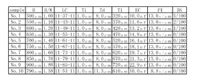
- FIG. 3 is a longitudinal sectional view taken along line SS of FIG. 4 shows a sample No. for verification. 1-No. It is a figure which shows 10 specifications and characteristics (electrostatic capacity, electric field strength, and bending strength). 5 shows the verification sample No. 1 shown in FIG. 1-No.
- FIG. 9 is a diagram showing a self-alignment effect of 9.
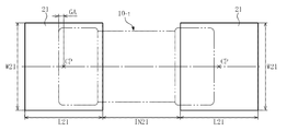
- FIG. 6 is an explanatory diagram of a method for confirming the self-alignment effect.
- FIG. 7 is an explanatory diagram of a method for confirming the self-alignment effect.
- FIG. 8 is a longitudinal sectional view corresponding to FIG. 3 of a multilayer ceramic capacitor (second embodiment) to which the present invention is applied.
- FIG. 11-No. It is a figure which shows the
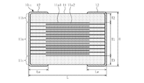
- FIGS. 1 to 3 show a multilayer ceramic capacitor 10-1 (first embodiment) to which the present invention is applied.
- the multilayer ceramic capacitor 10-1 includes a capacitor body 11 having a multilayer structure and a pair of external electrodes 12, and has a substantially rectangular parallelepiped shape defined by a length L, a width W, and a height H.
- This multilayer ceramic capacitor 10-1 satisfies the condition of height H> width W, more specifically, the condition of length L> height H> width W. *
- the capacitor body 11 includes a capacitor portion 11b in which a plurality of internal electrode layers 11a1 are stacked via a ceramic layer 11a2, a ceramic first protection portion 11b, and a ceramic second protection portion 11c.
- the first protective portion 11b, the capacitor portion 11a, and the second protective portion 11c are arranged in layers in this order.
- the capacitor body 11 also has a substantially rectangular parallelepiped shape defined by the length, width and height, and satisfies the condition of height> width, more specifically, the condition of length> height> width.
- a plurality (20 layers in the figure) of the internal electrode layers 11a1 included in the capacitor portion 11a are rectangles having substantially the same contour shapes, and the thicknesses thereof are also substantially equal.
- the ceramic layers 11a2 (layers including both the portion sandwiched between the adjacent internal electrode layers 11a1 and the both sides in the length direction that are not sandwiched, 19 layers in the figure) existing between the adjacent internal electrode layers 11a1 are respectively Are substantially the same, and are larger than the contour shape of the internal electrode layer 11a1, and the thicknesses thereof are also substantially equal.
- the plurality of internal electrode layers 11a1 are alternately shifted in the length direction, and the edge of the odd-numbered internal electrode layer 11a1 from the top in FIG. 3 is electrically connected to one of the external electrodes 12 (left side in FIG. 3). Further, the edge of the even-numbered internal electrode layer 11a1 from the top in FIG. 3 is electrically connected to the other external electrode 12 (the right side in FIG. 3).
- the plurality of internal electrode layers 11a1 included in the capacitor portion 11a are made of conductors having substantially the same composition.
- a good conductor mainly composed of nickel, copper, palladium, platinum, silver, gold, an alloy thereof or the like can be used.
- the “conductor having substantially the same composition” here refers to a conductor having a slightly different composition within an allowable range due to the degree of sintering and the like in addition to the conductor having the same composition.
- the ceramic layer 11a2 existing between the adjacent internal electrode layers 11a1 includes ceramics having substantially the same composition and substantially the same dielectric constant, including the first protective part 11b and the second protective part 11c.
- This ceramic is preferably a dielectric ceramic mainly composed of barium titanate, strontium titanate, calcium titanate, magnesium titanate, calcium zirconate, calcium zirconate titanate, barium zirconate, titanium oxide and the like.
- ⁇ > 1000 or class 2 (high dielectric constant) dielectric ceramics can be used.
- Ceramics with substantially the same composition and the same dielectric constant refers to ceramics having the same composition and dielectric constant as well as ceramics in which at least one of the composition and the dielectric constant is slightly different within an allowable range due to the degree of sintering, etc. Point to. *
- Each external electrode 12 is provided so as to cover a length direction end face of the capacitor body 11 and a part of four side faces adjacent to the end face.
- Le indicates the length of the portion of each external electrode 12 that covers a part of the four side surfaces of the capacitor body 11.
- each external electrode 12 has a two-layer structure of a base film in close contact with the outer surface of the capacitor body 11 and a surface film in close contact with the outer surface of the base film, or between the base film and the surface film. It has a multilayer structure having at least one intermediate film.
- the base film is made of, for example, a baked film, and a good conductor mainly composed of nickel, copper, palladium, platinum, silver, gold, or an alloy thereof can be used for the baked film.
- the surface film is composed of, for example, a plating film, and a good conductor whose main component is tin, palladium, gold, zinc, an alloy thereof or the like can be used for the plating film.
- the intermediate film is made of, for example, a plating film.
- a good conductor whose main component is preferably platinum, palladium, gold, copper, nickel, or an alloy thereof can be used. *
- the multilayer ceramic capacitor 10-1 shown in FIGS. 1 to 3 has a condition of 1.10 ⁇ height H / width W ⁇ 1.70, preferably 1.30 ⁇ height H / width W ⁇ 1.60. The condition is satisfied. The significance of these conditions will be described in detail later. *
- the ceramic layer 11a2 the first protective portion 11b, and the second protective portion 11c of the capacitor portion 11a are mainly composed of barium titanate
- the internal electrode layer 11a1 of the capacitor portion 11a is mainly composed of nickel
- titanium prepare ceramic slurry containing additives such as barium acid powder, ethanol (solvent), polyvinyl butyral (binder) and dispersant, and add additives such as nickel powder, terpineol (solvent), ethyl cellulose (binder) and dispersant.
- An electrode paste is prepared. *
- the ceramic slurry is coated on the carrier film and dried to produce a first green sheet.
- a coating device such as a die coater and a drying device
- the electrode paste is printed on the first green sheet in a zigzag or matrix form and dried to form a second pattern of patterns for internal electrode layers. Make a green sheet.
- unit sheets punched from the first green sheet are stacked up to a predetermined number and thermocompression-bonded, and a portion corresponding to the second protection portion 11c is formed. Make it.
- unit sheets (including the internal electrode layer pattern group) punched out from the second green sheet are stacked up to a predetermined number and thermocompression bonded to produce a portion corresponding to the capacitor portion 11a.
- the unit sheets punched from the first green sheet are stacked up to a predetermined number and subjected to thermocompression bonding, thereby producing a portion corresponding to the first protection portion 11b.
- final press-bonding apparatuses such as a hot isostatic pressing machine, is finally press-bonded finally, and an unbaking lamination sheet is produced.
- the unfired laminated sheet is cut into a lattice shape, and an unfired chip corresponding to the capacitor body 11 is produced.
- a firing apparatus such as a tunnel-type firing furnace, a number of unfired chips are fired in a reducing atmosphere or a low oxygen partial pressure atmosphere with a temperature profile corresponding to barium titanate and nickel (debindering) A firing chip corresponding to the capacitor body 11 is manufactured.
- an applicator such as a roller applicator
- an electrode paste (applying the electrode paste for the internal electrode layer) is applied to both ends in the length direction of the fired chip, and a baking process is performed in the same atmosphere as described above.
- a base film is formed, and a surface film, or an intermediate film and a surface film are formed thereon by a plating process such as electrolytic plating, thereby producing an external electrode.
- the base film of the external electrode may be produced by applying an electrode paste to both ends of the non-fired chip in the length direction and drying it, and then firing it simultaneously with the non-fired chip.
- each external electrode 12 has a three-layer structure of a base film mainly containing nickel, an intermediate film mainly containing copper, and a surface film mainly containing tin.
- Sample No. 1-No. 9 is the length L is 1000 ⁇ m, the width W is 500 ⁇ m, the thickness T2 of the first protection portion 11b is 88 ⁇ m, and the number of ceramic layers constituting the first protection portion 11b (the values shown on the left side of the layer structure LC). ) Is 11 layers.
- the thickness T3 of the second protective part 11c is 88 .mu.m.
- the number of ceramic layers constituting the second protective part 11c (the value shown on the right side of the layer structure LC) is 11 layers.
- the thickness Ti of the electrode layer 11a1 is 1.0 ⁇ m, the thickness Td of the ceramic layer 11a2 of the capacitor part 11a, the thickness Td of the ceramic layer constituting the first protection part 11b, and the ceramic constituting the second protection part 11c.
- the thickness Td of each layer is 8.0 ⁇ m
- the thickness of each external electrode 12 is 10 ⁇ m
- the length Le (see FIGS. 1 to 3) of the part covering the four side surfaces of the capacitor body 11 is 250 ⁇ m.
- the layer structure By increasing the numerical value (the sum of the number of internal electrode layers 11a1 and the number of ceramic layers 11a2) shown in the center of the LC, the thickness T1 and the height H of the capacitor portion 11a are gradually increased.
- n1 is the number of ceramic layers constituting the first protective part 11b
- m is the number of internal electrode layers 11a1 of the capacitor part 11a and the ceramic layer 11a2.
- N2 is the number of ceramic layers constituting the second protective part 11c, and the number of layers is based on the number of stacked layers in the stacking step of the manufacturing example.
- (m ⁇ 1) / 2 + 1 corresponds to the number of internal electrode layers 11a1
- (m ⁇ 1) / 2 corresponds to the number of ceramic layers 11a2.
- sample No. 1-No. 9 of sample no. 2 to No. Although sample No. 9 satisfies the condition of height H> width W, sample no. 1 does not satisfy the same condition because the height H is the same as the width W. That is, sample no.
- Reference numeral 1 is a conventional multilayer ceramic capacitor. 2 to No. Reference numeral 9 denotes a multilayer ceramic capacitor corresponding to the multilayer ceramic capacitor 10-1 shown in FIGS. *
- Sample No. 10 The thickness Td of the ceramic layer 11a2 of the capacitor portion 11a, the thickness Td of the ceramic layer constituting the first protective portion 11b, and the thickness Td of the ceramic layer constituting the second protective portion 11c are all 11.3 ⁇ m ⁇
- the thickness T2 of the first protective part 11b is 124.3 ⁇ m and the thickness T3 of the second protective part 11c is 124.3 ⁇ m. 1-No. 9 and different. That is, sample no.
- Reference numeral 10 denotes a multilayer ceramic capacitor corresponding to the multilayer ceramic capacitor 10-1 shown in FIGS. 1 to 3 because the condition of height H> width W is satisfied although the thickness Td is different. *
- the capacitance EC shown in FIG. 1-No. 100 of 10 were prepared, and each electrostatic capacity was measured using HP4284A (made by Agilent), and the average value for each sample was calculated. Further, the electric field strength FI shown in FIG. 4 was calculated from the thickness Td of the ceramic layer with respect to the rated voltage (100 V). *
- the flexural strength BS shown in FIG. 1-No. 100 pieces of 10 are prepared, and each is soldered to one surface of a glass epoxy substrate in accordance with JIS-C-6484, and then the state where 45 mm on both sides from the sample soldering portion on one surface of the glass epoxy substrate is supported by a piece.
- the part corresponding to the sample soldering part on the other surface is deformed by pressing it down 10 mm at a constant speed of 0.5 mm / sec with a jig (the pressing part is made of a curved surface having a curvature radius of 230 mm).
- the number of samples with a volume reduction of 12.5% or more was counted. *
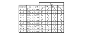
- FIG. 1-No. 9 shows the self-alignment effect.
- Reference numeral 1 is a conventional multilayer ceramic capacitor.
- Reference numeral 9 denotes a multilayer ceramic capacitor corresponding to the multilayer ceramic capacitor 10-1 shown in FIGS. *
- sample no. 1-No. 80 pieces of 9 are prepared and 36 test boards are prepared.
- 20 sets of two rectangular conductor pads 21 having a length L21 of 500 ⁇ m and a width W21 of 550 ⁇ m are formed with an interval IN21 of 500 ⁇ m (see FIG. 6).
- 6 and 7 indicate the center CP of the conductor pad 21, and the alternate long and short dash line indicates the center line in the width direction of the conductor pad 21 forming a set.
- cream solder was applied to the upper surface of each of the conductor pads 21 of the four test substrates in a thickness of 0.20 mm. 1 (20 per test board).
- 20 sample Nos. 1 is installed, each sample No. 1 so that the center line in the width direction of the conductor pad 21 coincides with the center line in the width direction of the pair of conductor pads 21.
- a gap GA of 75 ⁇ m is generated between the end face of each external electrode 12 and the center CP of the conductor pad 21 (see FIG. 6).
- 20 sample Nos On the second test substrate. 1 is mounted, the gap GA is set to 50 ⁇ m, and 20 sample numbers are set on the third test substrate.
- the deviation GA is set to 25 ⁇ m, and 20 sample numbers are set on the fourth test board.
- the deviation GA is set to 10 ⁇ m (see the deviation GA in FIG. 5).
- Other sample No. 2 to No. For sample No. 9, sample no. 1 is installed. *
- sample no. 1-No. Heat treatment such as reflow soldering is applied to a total of 36 test substrates on which 9 is mounted, and the external electrodes 12 of the mounted samples 1 to 9 are joined to the conductor pads 21 via solder. Subsequently, whether or not the deviation GA becomes zero in the heat treatment process (whether or not the self-alignment effect is obtained) is confirmed for each test substrate using an optical microscope (see FIG. 7). *
- the sample No. 1 shown in FIG. In comparison with the electrostatic capacity EC of Sample 1, the sample No. 2 to No.
- the capacitance EC of 9 increases as the height H increases.
- the increase in the capacitance EC is due to the increase in the number of layers of the capacitor portion 11a (the number of layers of the internal electrode layer 11a1). 2 to No. From the increasing tendency of the electrostatic capacity EC of 9, it can be said that the capacity can be increased without increasing the height H so much.
- sample No. The sample No. 1 has a height H lower than that in the case of stacking and integrating two pieces of one. It can be said that a capacitance EC that is twice or more than 1 can be easily secured. *
- the sample No. shown in FIG. In comparison with the flexural strength BS of No. 1, sample No. 2 to No.
- the flexural strength BS of 9 increases as the height H increases.
- Sample No. The flexural strength BS of 2 is 2/100.
- the width W and the height H are 1.10 ⁇ height H / width W. If the conditions are satisfied, it can be said that mounting on a circuit board or the like can be performed satisfactorily.
- Sample No. 4 to No. Considering that the flexural strength BS of No. 9 is 0/100, if the width W and the height H satisfy the condition of 1.30 ⁇ height H / width W, they are mounted on a circuit board or the like. It can be said that can be performed even better. *
- sample No. shown in FIG. Compared to the self-alignment effect of Sample No. 9, 2 to No.
- the self-alignment effect of 8 is improved.
- Sample No. Although the self-alignment effect of No. 8 includes the effect ( ⁇ mark), since the evaluation is not a serious problem in actual mounting, the width W and the height H are the height H / width W. If the condition of ⁇ 1.70 is satisfied, it can be said that mounting on a circuit board or the like can be performed satisfactorily.
- Sample No. 2 to No. In view of the fact that all the self-alignment effects of No. 7 are highly effective (circles), if the width W and the height H satisfy the condition of height H / width W ⁇ 1.60, circuit boards, etc. It can be said that it can be implemented even better. *
- the length Le of the part covering each of the four side surfaces of the capacitor body 11 in each external electrode 12 is 250 ⁇ m.
- the self-alignment effect described above mainly affects the end face of each external electrode 12. Since it depends on the adhesion contour of the solder, the self-alignment effect can be similarly obtained even if the length Le is changed to a value other than 250 ⁇ m.
- the width W and the height H satisfy the condition of 1.10 ⁇ height H / width W ⁇ 1.70. Then, in addition to being effective for increasing the capacity, it is possible to satisfactorily mount the circuit board or the like based on the improvement of the flexural strength BS and the self-alignment effect. In addition, if the width W and the height H satisfy the condition of 1.30 ⁇ height H / width W ⁇ 1.60, it is effective for increasing the capacity, as well as for circuit boards and the like. Mounting can be performed even better. *
- FIG. 8 shows a multilayer ceramic capacitor 10-2 (second embodiment) to which the present invention is applied.
- This multilayer ceramic capacitor 10-2 includes the multilayer ceramic capacitor 10-1 (first embodiment) shown in FIGS. 1 to 3, the capacitor portion 11a, the first protection portion 11b, and the second protection portion 11c of the capacitor body 11.
- the condition of the thickness T3 of the second protection part 11c> the thickness T2 of the first protection part 11b more specifically, the thickness T1 of the capacitor part 11a> the thickness T3 of the second protection part 11c> the first protection part 11b. Is different in that the condition of the thickness T2 is satisfied.
- Other configurations are the same as those of the multilayer ceramic capacitor 10-1 shown in FIGS. *
- the multilayer ceramic capacitor 10-2 shown in FIG. 8 has a condition of 1.18 ⁇ thickness T3 / thickness T2 ⁇ 4.36, preferably 2.18 ⁇ thickness T3 / thickness T2 ⁇ 3.64. Is satisfied.
- the multilayer ceramic capacitor 10-2 shown in FIG. 8 has a condition of 0.028 ⁇ (thickness T3 ⁇ thickness T2) / height H ⁇ 0.350, preferably 0.159 ⁇ (thickness T3- The condition of (thickness T2) / height H ⁇ 0.297 is satisfied. The significance of these conditions will be described in detail later. *
- FIG. 11-No. 23 shows specifications and characteristics (flexure strength BS).
- the sample No. shown in FIG. 2 specifications and characteristics (flexure strength BS) are shown.
- These sample Nos. 11-No. 23 is manufactured according to the above manufacturing example (see the first embodiment column), and the main component of the internal electrode layer 11a1 of the capacitor portion 11a is nickel, and the ceramic layer 11a2 of the capacitor portion 11a and the second
- the main component of the first protective part 11b and the second protective part 11c is barium titanate, and each external electrode 12 has a base film mainly composed of nickel, an intermediate film mainly composed of copper, and a surface mainly composed of tin. It is a three-layer structure of a film. *
- Sample No. 11-No. 23 length L is 1000 ⁇ m, width W is 500 ⁇ m
- the thickness T1 of the capacitor portion 11a is 370 ⁇ m.
- the sum of the number of internal electrode layers 11a1 and the number of ceramic layers 11a2 in the capacitor portion 11a (the value shown in the center of the layer structure LC) is 43 layers.
- First protection The thickness T2 of the part 11b is 88 ⁇ m.
- the number of ceramic layers constituting the first protection part 11b (the value shown on the left side of the layer structure LC) is 11 layers.
- the thickness Ti of the internal electrode layer 11a1 of the capacitor part 11a is The thickness Td of the ceramic layer 11a2 of the 1.0 ⁇ m capacitor portion 11a, the thickness Td of the ceramic layer constituting the first protection portion 11b, and the thickness Td of the ceramic layer constituting the second protection portion 11c are all 8.0 ⁇ m ⁇ Although the thickness of each external electrode 12 is 10 ⁇ m and the length Le (see FIG. 8) covering a part of the four side surfaces of the capacitor body 11 is 250 ⁇ m, the layer is common. Numerical values shown on the right side of the LC The thickness T3 and the height H of the second protective portion 11c by increasing the number of layers) of the ceramic layer constituting the second protective portion 11c is gradually increased.
- Reference numeral 23 is a multilayer ceramic capacitor corresponding to the multilayer ceramic capacitor 10-2 shown in FIG. 8 because the condition of thickness T3> thickness T2 is satisfied in addition to the condition of height H> width W. . *
- Sample No. 11-No. 23 is the thickness of the first protective part 11b in consideration of satisfying the condition of 1.10 ⁇ height H / width W ⁇ 1.70 described at the end of the first embodiment column. Focusing on T2 and the thickness T3 of the second protection portion 11c, if the thickness T2 and the thickness T3 satisfy the condition of 1.18 ⁇ thickness T3 / thickness T2 ⁇ 4.36, the capacity is increased. Of course, it can be said that it can be mounted on a circuit board or the like satisfactorily. *
- Sample No. 11-No. 23, sample no. 15-No. Considering that 20 satisfies the condition of 1.30 ⁇ height H / width W ⁇ 1.60 described at the end of the first embodiment column, the thickness of the first protective portion 11b Focusing on T2 and the thickness T3 of the second protection portion 11c, if the thickness T2 and the thickness T3 satisfy the condition of 2.18 ⁇ thickness T3 / thickness T2 ⁇ 3.64, the capacity is increased. It can be said that it can be mounted on a circuit board or the like even more effectively. *
- sample no. 11-No. 23 is the thickness of the first protective part 11b in consideration of satisfying the condition of 1.10 ⁇ height H / width W ⁇ 1.70 described at the end of the first embodiment column.
- thickness T2 and thickness T3 and height H of second protection part 11c are 0.028 ⁇ (thickness T3 ⁇ thickness T2) / height H ⁇ 0. If the condition of ..350 is satisfied, it can be said that it can be effectively mounted on a circuit board or the like as well as effective in increasing the capacity.
- Sample No. 11-No. 23, sample no. 15-No. Considering that 20 satisfies the condition of 1.30 ⁇ height H / width W ⁇ 1.60 described at the end of the first embodiment column, the thickness of the first protective portion 11b Focusing on T2 and the thickness T3 and the height H of the second protective portion 11c, the thickness T2, the thickness T3, and the thickness H are 0.159 ⁇ (thickness T3 ⁇ thickness T2) / height H ⁇ 0. If the condition of .297 is satisfied, it can be said that the mounting on a circuit board or the like can be performed more satisfactorily as well as effective in increasing the capacity. *
- the multilayer ceramic capacitor 10-1 shown in FIGS. 1 to 3 and the multilayer ceramic capacitor 10-2 shown in FIG. 8 satisfy the condition of length L> height H> width W. Although shown, if at least the condition of height H> width W is satisfied, the same effect as described above can be obtained regardless of the dimensional relationship between the length L and the height H.
- 10-1, 10-2 multilayer ceramic capacitor, 11 ... capacitor body, 11a ... capacitance part, 11a1 ... internal electrode layer, 11a2 ... ceramic layer, 11b ... first protection part, 11c ... second protection part, 12 ... external Electrode, L: length of the multilayer ceramic capacitor, W: width of the multilayer ceramic capacitor, H: height of the multilayer ceramic capacitor, T1: thickness of the capacitor portion of the capacitor body, T2: thickness of the first protective portion of the capacitor body T3 is the thickness of the second protective part of the capacitor body.
Landscapes
- Engineering & Computer Science (AREA)
- Power Engineering (AREA)
- Microelectronics & Electronic Packaging (AREA)
- Manufacturing & Machinery (AREA)
- Chemical & Material Sciences (AREA)
- Ceramic Engineering (AREA)
- Inorganic Chemistry (AREA)
- Ceramic Capacitors (AREA)
- Fixed Capacitors And Capacitor Manufacturing Machines (AREA)
Abstract
Description
厚さTdと、第1保護部11bを構成するセラミック層の厚さTdと、第2保護部11cを構成するセラミック層の厚さTdが何れも8.0μm・各外部電極12の厚さが10μmで、コンデンサ本体11の4側面の一部を覆う部分の長さLe(図1~図3を参照)が250μmである点で共通しているものの、層構成LCの中央に示した数値(内部電極層11a1の層数とセラミック層11a2の層数との和)を増やすことによって容量部11aの厚さT1と高さHが徐々に増加している。
・容量部11aの厚さT1が370μm・容量部11aの内部電極層11a1の層数とセラミック層11a2の層数との和(層構成LCの中央に示した数値)が43層・第1保護部11bの厚さT2が88μm・第1保護部11bを構成するセラミック層の層数(層構成LCの左側に示した数値)が11層・容量部11aの内部電極層11a1の厚さTiが1.0μm・容量部11aのセラミック層11a2の厚さTdと、第1保護部11bを構成するセラミック層の厚さTdと、第2保護部11cを構成するセラミック層の厚さTdが何れも8.0μm・各外部電極12の厚さが10μmで、コンデンサ本体11の4側面の一部を覆う部分の長さLe(図8を参照)が250μmである点で共通しているものの、層構成LCの右側に示した数値(第2保護部11cを構成するセラミック層の層数)を増やすことによって第2保護部11cの厚さT3と高さHが徐々に増加している。
Claims (7)
- 積層構造のコンデンサ本体と1対の外部電極とを備え、長さLと幅Wと高さHで規定された略直方体状の積層セラミックコンデンサであって、 前記幅Wと前記高さHが、1.10≦H/W≦1.70の条件を満足している、 積層セラミックコンデンサ。
- 請求項1に記載した条件が、1.30≦H/W≦1.60である、 請求項1に記載の積層セラミックコンデンサ。
- 前記コンデンサ本体は、複数の内部電極層がセラミック層を介して積層された容量部と、セラミック製の第1保護部と、セラミック製の第2保護部とを、高さ方向に第1保護部-容量部-第2保護部の順で層状に並ぶように有しており、 前記コンデンサ本体の第1保護部の厚さをT2とし第2保護部の厚さをT3としたとき、前記厚さT2と前記厚さT3が、1.18≦T3/T2≦4.36の条件を満足している、 請求項1に記載の積層セラミックコンデンサ。
- 請求項3に記載した条件が、2.18≦T3/T2≦3.64である、 請求項3に記載の積層セラミックコンデンサ。
- 前記コンデンサ本体は、複数の内部電極層がセラミック層を介して積層された容量部と、セラミック製の第1保護部と、セラミック製の第2保護部とを、高さ方向に第1保護部-容量部-第2保護部の順で層状に並ぶように有しており、 前記コンデンサ本体の第1保護部の厚さをT2とし第2保護部の厚さをT3としたとき、前記厚さT2と前記厚さT3と前記高さHが、0.028≦(T3-T2)/H≦0.350の条件を満足している、 請求項1又は3に記載の積層セラミックコンデンサ。
- 請求項5に記載した条件が、0.159≦(T3-T2)/H≦0.297である、 請求項5に記載の積層セラミックコンデンサ。
- 前記長さLと前記幅Wと前記高さHが、L>H>Wの条件を満足している、 請求項1~6の何れか1項に記載の積層セラミックコンデンサ。
Priority Applications (5)
| Application Number | Priority Date | Filing Date | Title |
|---|---|---|---|
| HK16109036.9A HK1221066B (zh) | 2013-06-19 | 2014-06-19 | 层叠陶瓷电容器 |
| KR1020157026891A KR101812475B1 (ko) | 2013-06-19 | 2014-06-19 | 적층 세라믹 콘덴서 |
| US14/888,403 US9941050B2 (en) | 2013-06-19 | 2014-06-19 | Multilayer ceramic capacitor |
| CN201480034968.4A CN105308697B (zh) | 2013-06-19 | 2014-06-19 | 层叠陶瓷电容器 |
| PH12015502559A PH12015502559B1 (en) | 2013-06-19 | 2015-11-10 | Multilayer ceramic capacitor |
Applications Claiming Priority (4)
| Application Number | Priority Date | Filing Date | Title |
|---|---|---|---|
| JP2013-128512 | 2013-06-19 | ||
| JP2013128512 | 2013-06-19 | ||
| JP2014-123023 | 2014-06-16 | ||
| JP2014123023A JP6798766B2 (ja) | 2013-06-19 | 2014-06-16 | 積層セラミックコンデンサ |
Publications (1)
| Publication Number | Publication Date |
|---|---|
| WO2014203948A1 true WO2014203948A1 (ja) | 2014-12-24 |
Family
ID=52104674
Family Applications (1)
| Application Number | Title | Priority Date | Filing Date |
|---|---|---|---|
| PCT/JP2014/066223 Ceased WO2014203948A1 (ja) | 2013-06-19 | 2014-06-19 | 積層セラミックコンデンサ |
Country Status (6)
| Country | Link |
|---|---|
| US (1) | US9941050B2 (ja) |
| JP (1) | JP6798766B2 (ja) |
| KR (1) | KR101812475B1 (ja) |
| CN (1) | CN105308697B (ja) |
| PH (1) | PH12015502559B1 (ja) |
| WO (1) | WO2014203948A1 (ja) |
Families Citing this family (10)
| Publication number | Priority date | Publication date | Assignee | Title |
|---|---|---|---|---|
| US9627142B2 (en) * | 2013-09-24 | 2017-04-18 | Samsung Electro-Mechanics Co., Ltd. | Multilayer ceramic capacitor and board for mounting of the same |
| JP6632808B2 (ja) * | 2015-03-30 | 2020-01-22 | 太陽誘電株式会社 | 積層セラミックコンデンサ |
| KR101771798B1 (ko) * | 2015-08-26 | 2017-08-25 | 삼성전기주식회사 | 적층 세라믹 커패시터 및 그 실장 기판 |
| JP7302940B2 (ja) * | 2017-01-27 | 2023-07-04 | 太陽誘電株式会社 | 積層セラミック電子部品 |
| JP7356207B2 (ja) | 2017-12-22 | 2023-10-04 | 太陽誘電株式会社 | 積層セラミック電子部品、積層セラミック電子部品実装基板及び積層セラミック電子部品包装体 |
| US10957488B2 (en) | 2018-04-20 | 2021-03-23 | Samsung Electro-Mechanics Co., Ltd. | Multilayer ceramic electronic component |
| JP7182926B2 (ja) | 2018-07-17 | 2022-12-05 | 太陽誘電株式会社 | 積層セラミック電子部品 |
| KR102048155B1 (ko) * | 2018-09-05 | 2019-11-22 | 삼성전기주식회사 | 적층 세라믹 전자부품 |
| KR102900299B1 (ko) * | 2020-12-23 | 2025-12-12 | 삼성전기주식회사 | 적층 세라믹 전자부품 및 이의 실장 기판 |
| JP2023079253A (ja) * | 2021-11-29 | 2023-06-08 | 太陽誘電株式会社 | 積層セラミック電子部品 |
Citations (5)
| Publication number | Priority date | Publication date | Assignee | Title |
|---|---|---|---|---|
| JPH08130160A (ja) * | 1994-10-31 | 1996-05-21 | Murata Mfg Co Ltd | 積層セラミック電子部品の製造方法 |
| JP2004193352A (ja) * | 2002-12-11 | 2004-07-08 | Taiyo Yuden Co Ltd | 積層コンデンサ及び積層コンデンサ実装体 |
| JP2005347288A (ja) * | 2004-05-31 | 2005-12-15 | Tdk Corp | 積層セラミックコンデンサの製造方法 |
| JP2012248846A (ja) * | 2011-05-26 | 2012-12-13 | Samsung Electro-Mechanics Co Ltd | 積層セラミックコンデンサの回路基板の実装構造 |
| JP2012248581A (ja) * | 2011-05-25 | 2012-12-13 | Tdk Corp | 積層コンデンサ及び積層コンデンサの製造方法 |
Family Cites Families (5)
| Publication number | Priority date | Publication date | Assignee | Title |
|---|---|---|---|---|
| JPH11251186A (ja) | 1998-02-26 | 1999-09-17 | Kyocera Corp | スタック型セラミックコンデンサ |
| JP4650007B2 (ja) * | 2005-02-01 | 2011-03-16 | 株式会社村田製作所 | 積層コンデンサ |
| KR101058697B1 (ko) * | 2010-12-21 | 2011-08-22 | 삼성전기주식회사 | 적층 세라믹 커패시터의 회로 기판 실장 구조, 실장 방법과 이를 위한 회로 기판의 랜드 패턴, 수평 방향으로 테이핑한 적층 세라믹 커패시터의 포장체 및 수평 방향 정렬방법 |
| JP5899699B2 (ja) * | 2011-08-10 | 2016-04-06 | Tdk株式会社 | 積層型コンデンサ |
| KR101309479B1 (ko) * | 2012-05-30 | 2013-09-23 | 삼성전기주식회사 | 적층 칩 전자부품, 그 실장 기판 및 포장체 |
-
2014
- 2014-06-16 JP JP2014123023A patent/JP6798766B2/ja active Active
- 2014-06-19 CN CN201480034968.4A patent/CN105308697B/zh active Active
- 2014-06-19 WO PCT/JP2014/066223 patent/WO2014203948A1/ja not_active Ceased
- 2014-06-19 US US14/888,403 patent/US9941050B2/en active Active
- 2014-06-19 KR KR1020157026891A patent/KR101812475B1/ko active Active
-
2015
- 2015-11-10 PH PH12015502559A patent/PH12015502559B1/en unknown
Patent Citations (5)
| Publication number | Priority date | Publication date | Assignee | Title |
|---|---|---|---|---|
| JPH08130160A (ja) * | 1994-10-31 | 1996-05-21 | Murata Mfg Co Ltd | 積層セラミック電子部品の製造方法 |
| JP2004193352A (ja) * | 2002-12-11 | 2004-07-08 | Taiyo Yuden Co Ltd | 積層コンデンサ及び積層コンデンサ実装体 |
| JP2005347288A (ja) * | 2004-05-31 | 2005-12-15 | Tdk Corp | 積層セラミックコンデンサの製造方法 |
| JP2012248581A (ja) * | 2011-05-25 | 2012-12-13 | Tdk Corp | 積層コンデンサ及び積層コンデンサの製造方法 |
| JP2012248846A (ja) * | 2011-05-26 | 2012-12-13 | Samsung Electro-Mechanics Co Ltd | 積層セラミックコンデンサの回路基板の実装構造 |
Also Published As
| Publication number | Publication date |
|---|---|
| HK1221066A1 (zh) | 2017-05-19 |
| US20160099108A1 (en) | 2016-04-07 |
| JP6798766B2 (ja) | 2020-12-09 |
| KR20150128760A (ko) | 2015-11-18 |
| PH12015502559B1 (en) | 2018-11-21 |
| CN105308697B (zh) | 2018-07-31 |
| CN105308697A (zh) | 2016-02-03 |
| KR101812475B1 (ko) | 2017-12-27 |
| PH12015502559A1 (en) | 2016-02-22 |
| US9941050B2 (en) | 2018-04-10 |
| JP2015026825A (ja) | 2015-02-05 |
Similar Documents
| Publication | Publication Date | Title |
|---|---|---|
| JP6798766B2 (ja) | 積層セラミックコンデンサ | |
| US10176924B2 (en) | Multilayer ceramic capacitor and board for mounting of the same | |
| EP2827351B1 (en) | Laminated ceramic chip electronic component | |
| EP2669914B1 (en) | Laminated chip electronic component, board for mounting the same and packing unit thereof | |
| JP5206440B2 (ja) | セラミック電子部品 | |
| US6829134B2 (en) | Laminated ceramic electronic component and method for manufacturing the same | |
| JP6058591B2 (ja) | 積層セラミック電子部品及び積層セラミック電子部品の実装基板 | |
| JP6180898B2 (ja) | 積層セラミックキャパシタ及び積層セラミックキャパシタの実装基板 | |
| HK1222038A1 (zh) | 贯通型层叠陶瓷电容器 | |
| CN105742059A (zh) | 贯通型层叠陶瓷电容器 | |
| KR20140085097A (ko) | 적층 세라믹 커패시터 및 그 제조 방법 | |
| KR102294680B1 (ko) | 적층 세라믹 전자부품 | |
| JP2015018891A (ja) | 積層セラミックコンデンサ | |
| JP7702261B2 (ja) | セラミック電子部品、回路基板およびセラミック電子部品の製造方法 | |
| KR19980086791A (ko) | 적층 세라믹 전자부품 | |
| JP6377957B2 (ja) | 積層セラミックコンデンサ | |
| JPH0563007B2 (ja) | ||
| JP6616929B2 (ja) | 積層セラミックコンデンサ | |
| KR20140148157A (ko) | 적층 세라믹 전자 부품의 제조 방법 및 이를 이용하여 제조된 적층 세라믹 전자 부품 | |
| JP6527612B2 (ja) | 積層セラミックコンデンサ | |
| HK1221066B (zh) | 层叠陶瓷电容器 | |
| CN115863054A (zh) | 层叠陶瓷电容器 |
Legal Events
| Date | Code | Title | Description |
|---|---|---|---|
| WWE | Wipo information: entry into national phase |
Ref document number: 201480034968.4 Country of ref document: CN |
|
| 121 | Ep: the epo has been informed by wipo that ep was designated in this application |
Ref document number: 14814312 Country of ref document: EP Kind code of ref document: A1 |
|
| ENP | Entry into the national phase |
Ref document number: 20157026891 Country of ref document: KR Kind code of ref document: A |
|
| WWE | Wipo information: entry into national phase |
Ref document number: 14888403 Country of ref document: US |
|
| WWE | Wipo information: entry into national phase |
Ref document number: 12015502559 Country of ref document: PH |
|
| NENP | Non-entry into the national phase |
Ref country code: DE |
|
| 122 | Ep: pct application non-entry in european phase |
Ref document number: 14814312 Country of ref document: EP Kind code of ref document: A1 |