WO2014203850A1 - 積層体、積層体の製造方法、光源装置用導光体及び光源装置 - Google Patents
積層体、積層体の製造方法、光源装置用導光体及び光源装置 Download PDFInfo
- Publication number
- WO2014203850A1 WO2014203850A1 PCT/JP2014/065883 JP2014065883W WO2014203850A1 WO 2014203850 A1 WO2014203850 A1 WO 2014203850A1 JP 2014065883 W JP2014065883 W JP 2014065883W WO 2014203850 A1 WO2014203850 A1 WO 2014203850A1
- Authority
- WO
- WIPO (PCT)
- Prior art keywords
- layer
- light
- cladding layer
- light source
- source device
- Prior art date
- Legal status (The legal status is an assumption and is not a legal conclusion. Google has not performed a legal analysis and makes no representation as to the accuracy of the status listed.)
- Ceased
Links
Images


Classifications
-
- G—PHYSICS
- G02—OPTICS
- G02B—OPTICAL ELEMENTS, SYSTEMS OR APPARATUS
- G02B6/00—Light guides; Structural details of arrangements comprising light guides and other optical elements, e.g. couplings
- G02B6/0001—Light guides; Structural details of arrangements comprising light guides and other optical elements, e.g. couplings specially adapted for lighting devices or systems
- G02B6/0011—Light guides; Structural details of arrangements comprising light guides and other optical elements, e.g. couplings specially adapted for lighting devices or systems the light guides being planar or of plate-like form
- G02B6/0065—Manufacturing aspects; Material aspects
-
- G—PHYSICS
- G02—OPTICS
- G02B—OPTICAL ELEMENTS, SYSTEMS OR APPARATUS
- G02B6/00—Light guides; Structural details of arrangements comprising light guides and other optical elements, e.g. couplings
- G02B6/0001—Light guides; Structural details of arrangements comprising light guides and other optical elements, e.g. couplings specially adapted for lighting devices or systems
- G02B6/0011—Light guides; Structural details of arrangements comprising light guides and other optical elements, e.g. couplings specially adapted for lighting devices or systems the light guides being planar or of plate-like form
- G02B6/0033—Means for improving the coupling-out of light from the light guide
- G02B6/0035—Means for improving the coupling-out of light from the light guide provided on the surface of the light guide or in the bulk of it
- G02B6/0045—Means for improving the coupling-out of light from the light guide provided on the surface of the light guide or in the bulk of it by shaping at least a portion of the light guide
-
- G—PHYSICS
- G02—OPTICS
- G02B—OPTICAL ELEMENTS, SYSTEMS OR APPARATUS
- G02B6/00—Light guides; Structural details of arrangements comprising light guides and other optical elements, e.g. couplings
- G02B6/0001—Light guides; Structural details of arrangements comprising light guides and other optical elements, e.g. couplings specially adapted for lighting devices or systems
- G02B6/0011—Light guides; Structural details of arrangements comprising light guides and other optical elements, e.g. couplings specially adapted for lighting devices or systems the light guides being planar or of plate-like form
- G02B6/0033—Means for improving the coupling-out of light from the light guide
- G02B6/005—Means for improving the coupling-out of light from the light guide provided by one optical element, or plurality thereof, placed on the light output side of the light guide
- G02B6/0051—Diffusing sheet or layer
-
- G—PHYSICS
- G02—OPTICS
- G02B—OPTICAL ELEMENTS, SYSTEMS OR APPARATUS
- G02B6/00—Light guides; Structural details of arrangements comprising light guides and other optical elements, e.g. couplings
- G02B6/0001—Light guides; Structural details of arrangements comprising light guides and other optical elements, e.g. couplings specially adapted for lighting devices or systems
- G02B6/0011—Light guides; Structural details of arrangements comprising light guides and other optical elements, e.g. couplings specially adapted for lighting devices or systems the light guides being planar or of plate-like form
- G02B6/0033—Means for improving the coupling-out of light from the light guide
- G02B6/005—Means for improving the coupling-out of light from the light guide provided by one optical element, or plurality thereof, placed on the light output side of the light guide
- G02B6/0055—Reflecting element, sheet or layer
-
- G—PHYSICS
- G02—OPTICS
- G02B—OPTICAL ELEMENTS, SYSTEMS OR APPARATUS
- G02B6/00—Light guides; Structural details of arrangements comprising light guides and other optical elements, e.g. couplings
- G02B6/0001—Light guides; Structural details of arrangements comprising light guides and other optical elements, e.g. couplings specially adapted for lighting devices or systems
- G02B6/0011—Light guides; Structural details of arrangements comprising light guides and other optical elements, e.g. couplings specially adapted for lighting devices or systems the light guides being planar or of plate-like form
- G02B6/0033—Means for improving the coupling-out of light from the light guide
- G02B6/0035—Means for improving the coupling-out of light from the light guide provided on the surface of the light guide or in the bulk of it
- G02B6/0036—2-D arrangement of prisms, protrusions, indentations or roughened surfaces
-
- G—PHYSICS
- G02—OPTICS
- G02B—OPTICAL ELEMENTS, SYSTEMS OR APPARATUS
- G02B6/00—Light guides; Structural details of arrangements comprising light guides and other optical elements, e.g. couplings
- G02B6/0001—Light guides; Structural details of arrangements comprising light guides and other optical elements, e.g. couplings specially adapted for lighting devices or systems
- G02B6/0011—Light guides; Structural details of arrangements comprising light guides and other optical elements, e.g. couplings specially adapted for lighting devices or systems the light guides being planar or of plate-like form
- G02B6/0033—Means for improving the coupling-out of light from the light guide
- G02B6/0058—Means for improving the coupling-out of light from the light guide varying in density, size, shape or depth along the light guide
- G02B6/0061—Means for improving the coupling-out of light from the light guide varying in density, size, shape or depth along the light guide to provide homogeneous light output intensity
Definitions
- the present invention relates to a laminate, a method for manufacturing the laminate, a light guide for a light source device, and a light source device.
- This application claims priority based on Japanese Patent Application No. 2013-127273 filed in Japan on June 18, 2013 and Japanese Patent Application No. 2013-163828 filed in Japan on August 7, 2013. The contents are incorporated herein.
- liquid crystal display devices used in mobile phones, notebook computers, liquid crystal televisions, video cameras, etc., backlight keys for mobile phones, backlight keyboards for personal computers, display devices such as display switches for electrical equipment and vehicles, ceiling lights, etc.
- light source devices used in lighting devices such as indoor lighting and lighting signs include direct light source devices and plates in which a plurality of linear light sources such as fluorescent lights and point light sources such as light emitting diodes are arranged in a housing.
- edge light type light source device in which a linear light source or a point light source is arranged on a side surface of a light guide.
- An edge light type light source device is usually composed of a light guide made of a transparent material such as a rectangular plate-like acrylic resin plate and a light source.
- the light source is disposed to face the side surface of the light guide.
- light from the light source is incident on the light guide from the side surface (light incident surface) and is the first surface (also referred to as the light exit surface) of the light guide or the second surface that is the surface facing the first surface.
- the light is emitted from an emission mechanism formed on the rear surface (also referred to as a back surface) or emitted from a light emission surface by a light emission means such as light diffusing particles contained in a light guide.
- the light incident from the side face is emitted not only from the light exit surface but also from the back surface of the light guide, so that the amount of light emitted from the light exit surface is reduced. Therefore, in the light source device, a light reflection layer is provided on the second surface of the light guide, that is, the surface facing the light output surface of the light guide, and the light emitted from the second surface is reflected and emitted from the light output surface. Or returning the light into the light guide to reuse the light emitted from the second surface.
- a light source device having excellent luminance can be obtained by using light from a light source with high efficiency.
- Patent Document 1 discloses a light source having an excellent brightness by providing a light reflecting layer that scatters and reflects light on the surface of a light guide having a core-clad structure, and combining the function of the light reflecting layer with the light guide.
- Device light guides have been proposed.
- the brightness that is, the luminance of the light guide is greatly influenced by the reflectance of the light reflection layer.
- the light guide for the light source device proposed in Patent Document 1 forms the light reflection layer by printing, the thickness of the light reflection layer is likely to cause unevenness in reflectance, and therefore the light guide is light-guided. Spots tend to appear on the body brightness.
- the light reflecting layer formed by printing is easily peeled off, and the durability of the light reflecting layer is not sufficient.
- the objective of this invention is providing the laminated body provided with the light reflection layer which adjustment of a reflectance is simple and excellent in durability.
- Another object of the present invention is to provide a method for producing a laminate comprising a light reflecting layer that is easy to adjust the reflectivity and has excellent durability, with reduced processing costs.
- a laminate including a core layer, a first cladding layer, a second cladding layer, and a light reflection layer, wherein the light reflection layer, the second cladding layer, the core layer, and the first cladding
- the layers are sequentially laminated, and the refractive index of the first cladding layer and the refractive index of the second cladding layer are lower than the refractive index of the core layer, and the thickness of the light reflecting layer is 50 ⁇ m or more .
- the laminate according to (1) further comprising light emitting means.
- the material for the light reflecting layer is any one of (1) to (4), which is at least one material selected from the group consisting of polyolefin resin, polyester resin, acrylic resin, and cellulose. Laminated body.
- At least one layer selected from the group consisting of a design layer and a light diffusion layer is further laminated on a surface facing the interface between the light reflection layer and the second cladding layer.
- the laminate according to (7). (9) Laminating the first cladding layer on the first surface of the core layer, laminating the second cladding layer on the second surface of the core layer, and forming a light reflecting layer on the second surface of the second cladding layer.
- a light guide for a light source device comprising the laminate according to any one of (1) to (8).
- a light source device comprising the laminate according to any one of (1) to (8) and a light source.
- a single-sided light source device comprising the laminate according to (6) and a light source.
- a double-sided light source device comprising the laminate according to (7) or (8) and a light source.
- the laminate of the present invention is easy to adjust the reflectance of the light reflecting layer and is excellent in durability. Moreover, the light source device which is excellent in brightness
- the light source device of the present invention has a laminated body including a light reflecting layer that is easy to adjust the reflectance and has excellent durability, and is excellent in luminance.
- FIG. 1 It is typical sectional drawing which shows the measuring apparatus which measures the average normal line brightness
- the interface between the core layer 11 and the first cladding layer 121 is referred to as the first surface of the core layer 11
- the interface between the core layer 11 and the second cladding layer 122 is referred to as the second surface of the core layer 11.
- the surface facing the interface between the first cladding layer 121 and the core layer 11 is the first surface of the first cladding layer 121
- the interface between the first cladding layer 121 and the core layer 11 is the first surface.
- the second surface of the first cladding layer 121 This is called the second surface of the first cladding layer 121, and in the second cladding layer, the interface between the second cladding layer 122 and the core layer 11 is the first surface of the second cladding layer 122, and the second cladding layer 122 and the core layer 11
- the surface facing the interface may be referred to as the second surface of the second cladding layer 122.
- the laminated body 10 (hereinafter simply referred to as the laminated body 10 of the present invention) which is one embodiment of the present invention includes a core layer 11, a first cladding layer 121, a second cladding layer 122, and a light reflecting layer. 14, the light reflecting layer 14, the second cladding layer 122, the core layer 11 and the first cladding layer 121 are sequentially stacked from the lower side in this order, The refractive index of the first cladding layer 121 and the refractive index of the second cladding layer 122 are lower than the refractive index of the core layer 11, and the adhesive layer 13 is further included between the second cladding layer 122 and the light reflecting layer 14.
- FIG. 10 The laminated body 10 (hereinafter simply referred to as the laminated body 10 of the present invention) which is one embodiment of the present invention includes a core layer 11, a first cladding layer 121, a second cladding layer 122, and a light reflecting layer. 14, the light reflecting layer 14, the second cladding layer
- FIG. 1 is a schematic perspective view showing an embodiment of a laminate 10 of the present invention.
- the laminated body 10 shown in FIG. 1 has a core layer 11, a first cladding layer 121, a second cladding layer 122, and a light reflecting layer 14, and is between the second cladding layer 122 and the light reflecting layer 14. Further, an adhesive layer 13 is included.
- the shape of the laminate 10 is not particularly limited as long as it is a plate shape.
- the laminate 10 having a plate shape means that the thickness T of the laminate 10 is small and the area of the first surface of the first cladding layer 121 is large.
- the thickness T of the laminate 10 is preferably 0.03 to 12 mm, more preferably 0.2 to 5.5 mm, and the area of the first surface of the first cladding layer 121 is 200 to 500,000 mm 2. Is preferable, and 500 to 250,000 mm 2 is more preferable.
- the thickness T of the stacked body 10 is the distance between the second surface of the second cladding layer 122 and the first surface of the first cladding layer 121.
- the thickness T of the stacked body 10 is measured by photographing a cross section of the stacked body 10 in the vertical direction with a microscope, and from any point on the second surface of the second cladding layer 122 to the first surface of the first cladding layer 121.
- the shortest dimension is measured at any five locations (provided that the light emitting means 15 is not provided), and the average value is calculated.
- the shape of the laminated body 10 for example, when viewed from the normal direction of the first surface of the first cladding layer 121, it is a polygonal shape such as a rectangle or a triangle; a circular shape such as a perfect circle or an ellipse. Is mentioned.
- the laminated body 10 when the laminated body 10 is used for the light source device 60, it is excellent in processability and easily allows light from the light source 31 to enter, and therefore, the laminated body 10 is preferably polygonal and rectangular. Is more preferable.
- the laminated body 10 may have a shape that is entirely curved or bent.
- the core layer 11 is not particularly limited as long as it is made of a highly transparent material, and can be appropriately selected according to the purpose of use. High transparency means that the transmittance value measured according to ISO 13468 is 50 to 100%.
- the material of the core layer 11 include acrylic resin, polycarbonate resin, alicyclic polyolefin resin, and glass. Among these materials for the core layer 11, acrylic resin, polycarbonate resin, and alicyclic polyolefin resin are preferable because they are lightweight and excellent in handleability.
- an acrylic resin is preferable because it is excellent in transparency and durability and is inexpensive.
- the acrylic resin include methyl methacrylate homopolymers, copolymers of methyl methacrylate and other monomers, and the like.
- these acrylic resins since it is more excellent in transparency and durability and is less expensive, it contains 50% by mass or more and less than 100% of methyl methacrylate homopolymer and methyl methacrylate unit based on the total mass of the copolymer.
- a copolymer is preferred.
- the content of methyl methacrylate units in the copolymer is preferably 50% by mass or more and less than 100% with respect to the total mass of the copolymer.
- the content is greater than or equal to 100% and less than 100%, more preferably greater than or equal to 70% and less than 100%.
- examples of other monomers include methyl acrylate, ethyl (meth) acrylate, n-propyl (meth) acrylate, n-butyl (meth) acrylate, n-hexyl (meth) acrylate, cyclohexyl (meth) acrylate, and the like.
- (meth) acrylate refers to acrylate or methacrylate.
- Polycarbonate resins and alicyclic polyolefin resins are preferred because of their excellent heat resistance and flame retardancy.
- a polycarbonate resin is preferable because the refractive index is high and the numerical aperture can be increased, so that leakage of light can be suppressed even when the laminate 10 is bent.
- the numerical aperture is an index that collects light. The larger the numerical aperture, the greater the amount of received light, and even when the laminate 10 is bent, light leakage can be kept low.
- the thickness of the core layer 11 is preferably 0.01 to 10 mm, and more preferably 0.05 to 5 mm, since the laminate 10 can be easily formed and the light source device 60 can be thinned.
- the thickness of the core layer 11 is a distance between the second surface and the first surface of the core layer 11.
- the thickness of the core layer 11 is obtained by photographing a cross section cut in the vertical direction of the core layer 11 with a microscope, and determining the shortest dimension from an arbitrary point on the second surface of the core layer 11 to the first surface of the core layer 11. It is calculated by measuring any five points (however, it is assumed that the light emitting means 15 is not provided) and obtaining an average value thereof.
- the first cladding layer 121 and the second cladding layer 122 are not particularly limited as long as they are made of a highly transparent material and have a refractive index lower than that of the core layer 11. It can be selected appropriately. As the material of the first cladding layer 121 and the second cladding layer 122, a material having a refractive index lower than that of the core layer 11 can be appropriately selected.
- examples of the material of the first cladding layer 121 and the second cladding layer 122 include a fluorine-containing olefin resin.
- the fluorine-containing olefin resin include a vinylidene fluoride homopolymer, a copolymer of vinylidene fluoride and tetrafluoroethylene, a copolymer of vinylidene fluoride and hexafluoropropylene, vinylidene fluoride and trifluoroethylene, and the like. And a copolymer of vinylidene fluoride, tetrafluoroethylene, and hexafluoropropylene.
- a vinylidene fluoride homopolymer is preferable because of excellent workability and moldability.
- examples of the material of the first cladding layer 121 and the second cladding layer 122 include fluorine-containing olefin resin and acrylic resin. Specific examples of the fluorine-containing olefin resin and acrylic resin are the same as described above, and the preferred range and reason are also the same as described above.
- Refractive index difference between the refractive index n 2 of the refractive index n 1 and the first cladding layer 121 and / or the second cladding layer 122 of the core layer 11 is preferably 0.001 or more, more preferably 0.01 or more.
- the refractive index difference between the refractive index n 2 of the refractive index n 1 of the core layer 11 and the first cladding layer 121 and / or the second cladding layer 122 is at least 0.001
- light core incident from the light incident surface The first clad layer 121 and / or the second clad layer 122 can propagate far away with little loss while totally reflecting the interface between the layer 11 and the first clad layer 121 and the interface between the core layer 11 and the second clad layer 122. Even if another layer is provided on the surface, there is little light leakage.
- the refractive index is a value measured with an Abbe refractometer using a sodium D line at 23 ° C. in accordance with ISO 13468.
- the thickness of the clad layer 12 is preferably 1 to 500 ⁇ m, and more preferably 3 to 100 ⁇ m because the laminate 10 having excellent handleability and light confinement efficiency can be obtained.
- the thickness of the first cladding layer 121 is measured by photographing a cross section cut in the vertical direction of the first cladding layer 121 with a microscope, and the first cladding layer 121 has a thickness from an arbitrary point on the second surface of the first cladding layer 121.
- the shortest dimension up to one surface is measured at any five locations (however, it is assumed that the light emitting means 15 is not provided), and the average value is calculated.
- the thickness of the second cladding layer 122 is measured by photographing a cross section of the second cladding layer 122 cut in the vertical direction with a microscope, and from the arbitrary point on the second surface of the second cladding layer 122.
- the shortest dimension up to one surface is measured at any five locations (however, it is assumed that the light emitting means 15 is not provided), and the average value is calculated.
- the ratio between the thickness of the core layer 11 and the thickness of the first cladding layer 121 and the ratio between the thickness of the core layer 11 and the thickness of the second cladding layer 122 are determined by the material of the core layer 11 and the first cladding layer 121 and the second cladding layer. It can be selected as appropriate depending on the material of the layer 122.
- the ratio of the volume of the core layer 11 to the volume of the first cladding layer 121 and the ratio of the volume of the core layer 11 to the volume of the second cladding layer 122 are determined by the material of the core layer 11 and the first cladding layer 121 and the second cladding layer. It can be selected as appropriate depending on the material of the layer 122.
- the material, thickness, and volume of the first cladding layer 121 provided on the surface of the core layer 11 and the second cladding layer 122 provided on the back surface of the core layer may be the same or different. .
- the side surface of the core layer 11 may or may not be covered with the first cladding layer 121 and / or the second cladding layer 122.
- the adhesive layer 13 has a role of bringing the first cladding layer 121 and the second cladding layer 122 and the light reflecting layer 14 into close contact with each other. If the adhesive layer 13 is a highly transparent material and has excellent adhesion to the first cladding layer 121 and the second cladding layer 122 and the light reflecting layer 14, the adhesive layer 13 is appropriately selected according to the purpose of use and the like. Can do. Examples of the material for the adhesive layer 13 include acrylic adhesives, natural rubber adhesives, synthetic rubber adhesives, silicone adhesives, urethane adhesives, and epoxy adhesives. 1 type may be used for these adhesives 13, and 2 or more types may be used together or mixed.
- acrylic adhesives acrylic adhesives, natural rubber adhesives, synthetic rubber adhesives, silicone adhesives, urethane adhesives, and epoxy adhesives are preferred because of their excellent adhesion.
- an adhesive, a natural rubber adhesive, and a synthetic rubber adhesive are more preferable, and an acrylic adhesive is more preferable.
- the thickness of the adhesive layer 13 is hardly deformed even when the laminated body 10 is bent, is excellent in the handleability of the laminated body 10, and adheres to the light reflecting layer 14 between the first cladding layer 121 and the second cladding layer 122. In view of excellent strength, it is preferably 1 to 500 ⁇ m, more preferably 3 to 100 ⁇ m.
- the thickness of the adhesive layer 13 is obtained by photographing a cross section of the adhesive layer 13 cut in the vertical direction with a microscope, and facing the interface between the adhesive layer 13 and the first cladding layer 121 or the second cladding layer 122 in the adhesive layer 13. Measure the shortest dimension from any point on the surface to the interface between the adhesive layer 13 and the first clad layer 121 or the second clad layer 122 (however, the portion where the light emitting means 15 is not provided) And calculating the average value.
- the first cladding layer 121 and the second cladding layer 122 and the adhesive layer 13 may be subjected to treatment such as corona discharge or plasma discharge to modify the surface.
- the light reflecting layer 14 is not particularly limited as long as it is a layer capable of scattering and reflecting light, and can be appropriately selected according to the purpose of use.
- the material of the light reflecting layer 14 include resin plates and resin films such as polyolefin resin, polyester resin, and acrylic resin; paper such as cellulose.
- resin plates and resin films such as polyolefin resin, polyester resin, and acrylic resin
- paper such as cellulose.
- the light reflecting layer 14 is hardly peeled even when the laminate 10 is bent, the durability of the laminate 10 is excellent, and it can also serve as a protective film for the laminate 10. Therefore, polyolefin resin, polyester resin, acrylic resin, and cellulose are preferable, and polyester resin is more preferable.
- the light reflecting layer 14 may be formed by foaming or may contain a pigment.
- the pigment include white pigments such as titanium oxide, barium sulfate, calcium carbonate, and magnesium carbonate. These pigments may be used alone or in combination of two or more. Among these pigments, a white pigment is preferable because of its high reflectance with respect to the entire visible light region.
- the reflectance of the light reflecting layer 14 greatly affects the luminance of the light source device 60, it is preferable to appropriately select a material or the like according to the target optical characteristics.
- the reflectance of the light reflecting layer 14 is preferably 70% or more, more preferably 70 to 100%, and further 75 to 100%. preferable.
- the reflectance of the light reflecting layer 14 is preferably 65% or less, more preferably 25 to 65%, and more preferably 30 to 30% in order to easily balance the luminance of both surfaces of the light source device 60. 60% or less is more preferable.
- the reflectance in this specification is 560 nm from the surface where the light reflecting layer 14 of the laminate 10 is not formed or the surface where the adhesive layer 13 of the light reflecting layer 14 is provided using a spectrocolorimeter. It can be calculated by irradiating light and measuring the reflectance of light at 560 nm.
- the thickness of the light reflecting layer 14 may be appropriately selected according to the reflectance of the light reflecting layer 14 and the use of the laminate 10. Even if the laminated body 10 is bent, the light reflecting layer 14 is hardly peeled off, the durability of the laminated body 10 is excellent, and the protective film of the laminated body 10 can be used, so 10 to 500 ⁇ m is preferable, and 50 to 200 ⁇ m is preferable. Is more preferable.
- the thickness of the light reflection layer 14 is determined by photographing a cross section cut in the vertical direction of the light reflection layer 14 with a microscope, and an arbitrary surface of the light reflection layer 14 facing the interface between the light reflection layer 14 and the core layer 11. From this point, the shortest dimension to the interface between the light reflecting layer 14 and the core layer 11 is measured at any five locations (however, the portion where the light emitting means 15 is not provided), and the average value is obtained. Calculated by
- the light reflecting layer 14 is provided on the second surface of the second cladding layer 122 via the adhesive layer 13.
- the light reflecting layer 14 may be provided on the first surface of the first cladding layer 121 via the adhesive layer 13.
- the light reflecting layer 14 is preferably provided only on the second surface of the laminate 10 because the light source device 60 is excellent in luminance.
- the light reflecting layer 14 may be provided on only one surface of the laminate 10 or may be provided on both surfaces of the laminate 10.
- the light reflecting layer 14 can be appropriately selected according to the use of the stacked body 10, but may cover the entire surface of the first cladding layer 121 and / or the second cladding layer 122. Alternatively, a part of the second cladding layer 122 may be covered.
- the adhesive layer 13 may be provided only in the region where the light reflecting layer 14 is provided. It may be provided including a region where the layer 14 is not provided.
- the light reflecting layer 14 covers a partial region of the second cladding layer 122, light is reflected in that region. Therefore, the light emitting means 15 is provided in that region or in the region facing the region of the first cladding layer. It is preferable to provide the light emitting means 15.
- FIG. 2 is a schematic perspective view showing an embodiment of a laminate 20 (hereinafter sometimes simply referred to as the laminate 20 of the present invention) which is an embodiment of the present invention.
- the laminate 20 of the present invention preferably further has a light emitting means 15 as shown in FIG. 2 includes a core layer 11, a first cladding layer 121 provided on the first surface of the core layer 11, and a second cladding layer 122 provided on the second surface of the core layer 11.
- the light reflecting layer 14 is provided on the second surface of the second cladding layer 122 via the adhesive layer 13, and the light emitting means 15 reaches the first cladding layer 121 from the first surface to the inside of the core layer 11. Is provided.
- the light emitting means 15 emits light propagating in the core layer 11 to the outside of the core layer 11.
- the light emitting means 15 penetrates the first cladding layer 121 and reaches the inside of the core layer 11, and the second cladding layer 122.
- Examples include a recess formed so as not to penetrate the clad layer 122 and to reach the inside of the core layer 11 from the interface between the second clad layer 122 and the core layer 11.
- the light emitting means 15 may be used alone or in combination of two or more. Among these light emitting means 15, since the light emission position can be easily controlled, a concave portion that penetrates the first cladding layer 121 and reaches the inside of the core layer 11 and a second cladding layer 122 that penetrates the inside of the core layer 11 are reached. A recess is preferable, and a recess that penetrates through the first cladding layer 121 and reaches the inside of the core layer 11 is more preferable.
- the light propagating through the core layer 11 due to reflection and refraction at the concave portion that penetrates the first cladding layer 121 and reaches the inside of the core layer 11 is emitted from the core layer 11 and emitted from the light emitting means 15 on the light emitting surface 17. Or, after reaching the light reflecting layer 14 and being scattered and reflected, the light is emitted from the light emitting surface 17, or is transmitted through the light reflecting layer 14 or returned to the core layer 11 to be guided and transmitted.
- the light emitting surface 17 refers to the first surface of the first cladding layer 121 of the stacked body 20.
- FIG. 3 is a schematic cross-sectional view showing an embodiment of a laminate in which the light reflecting layer 14 is not provided.
- the laminated body shown in FIG. 3 has a core layer 11, a first cladding layer 121 provided on the first surface of the core layer 11, and a second cladding layer 122 provided on the second surface of the core layer 11.
- the first cladding layer 121 is provided with light emitting means 15 that reaches the inside of the core layer 11 from the first surface.
- FIG. 4 is a schematic cross-sectional view showing an embodiment of a laminated body 30 (hereinafter sometimes simply referred to as the laminated body 30 of the present invention) which is an embodiment of the present invention.
- 4 includes a core layer 11, a first cladding layer 121 provided on the first surface of the core layer 11, and a second cladding layer 122 provided on the second surface of the core layer 11.
- a light reflecting layer 14 is provided on the surface of the second cladding layer 122 via the adhesive layer 13, and a light emitting means 15 is provided on the first cladding layer 121 from the first surface to the inside of the core layer 11. It has been.
- a part of the light A that has been totally reflected and propagated at the interface between the core layer 11 and the first cladding layer 121 and the second cladding layer 122 is refracted in the concave portion, and the refracted light B is It exits from the light exit surface 17. Further, a part of the light A is reflected by the concave portion, and the reflected light C is transmitted through the second cladding layer 122 and leaks because the light reflecting layer 14 is not provided.
- a part of the light A that has been totally reflected and propagated at the interface between the core layer 11 and the first cladding layer 121 and the second cladding layer 122 is refracted in the concave portion, and the refracted light B Exits from the light exit surface 17.
- a part of the light A is reflected by the concave portion, and the reflected light C is transmitted through the second cladding layer 122 and reflected by the light reflecting layer 14, and is emitted from the light emitting surface or returned to the core layer 11. Therefore, light leakage can be prevented in the laminate 30 shown in FIG.
- both surfaces can emit light while balancing the luminance of both surfaces of the laminated body 30.
- the size and position of the adhesive layer 13 and the light reflecting layer 14 are the shape of the light emitting means 15. Depending on the material of the core layer 11 and the cladding layer 12, etc., it can be appropriately selected. That is, according to the reflection angle of the light C, by providing the adhesive layer 13 and the light reflecting layer 14 having a necessary size at necessary positions, light leakage can be reduced and light emission excellent in luminance can be achieved. .
- the light emitting means 15 may be provided on the light emitting surface 17 or may be further provided on a surface other than the light emitting surface 17. When it is desired to emit light only on one side of the light source device 60, the light emitting means 15 may be provided only on one side of the laminated body 30 or on both sides of the laminated body 30. When it is desired to emit light from both surfaces of the light source device 60, the light emitting means 15 is preferably provided on both surfaces of the laminate 30 because it is easy to adjust the luminance of both surfaces of the light source device 60.
- the shape of the light emitting means 15 may be appropriately selected according to the light amount, the light guide distance, the form of light emission required for the laminate 30, and the like.
- Examples of the shape of the light emitting means 15 include a cone shape, a pyramid shape, a spherical shape, a prism shape such as a triangular prism and a quadrangular prism, and a line shape.
- the light emitting means 15 having these shapes may be used alone or in combination of two or more.
- the shape of the light emitting means 15 is a conical shape, a pyramid shape, or a sphere shape, the bottom surface of the cone shape, the pyramid shape, or the sphere shape exists on the surface on which the light emission means 15 is provided.
- the longitudinal direction of the prism may be parallel to the normal direction (also referred to as the light guide direction) of the light incident surface of the stacked body 30, or the light of the stacked body 30 It may be perpendicular to the normal direction of the incident surface, or may be oblique to the normal direction of the light incident surface of the laminate 30 at an arbitrary angle.
- the shape of the light emitting means 15 is a circular line when viewed from the upper side in the normal direction of the first surface of the core layer 11, a plurality of light emitting means 15 may be arranged concentrically.
- the concave portion is inclined with respect to the light incident surface of the laminated body 30, and the inclination angle of the concave portion It is preferable to set as described in the 2010/073726 pamphlet.
- the size of the light emitting means 15 is appropriately selected according to the materials of the core layer 11, the first cladding layer 121, the second cladding layer 122, and the light reflecting layer 14.
- the depth D of the light emitting means 15 is preferably a depth that penetrates the first cladding layer 121 and reaches the inside of the core layer 11 and does not penetrate the core layer 11. That is, it is preferable that d1 ⁇ D ⁇ d1 + d11 is satisfied by the depth D of the light emitting means 15, the thickness d1 of the first cladding layer 121, and the thickness d11 of the core layer 11.
- the size of the light emitting means 15 is within the above range, the light propagating through the core layer 11 can be sufficiently extracted from the core layer 11.
- the depth D of the light emitting means 15 represents the distance from the light emitting surface 17 to the deepest part of the light emitting means 15.
- the depth D of the light emitting means 15 is preferably 0.1 to 1000 ⁇ m, and more preferably 0.5 to 500 ⁇ m.
- the width W of the light emitting means 15 may be appropriately selected according to the materials of the core layer 11, the first cladding layer 121, the second cladding layer 122, and the light reflecting layer 14.
- the width W of the light emitting means 15 represents the maximum width in the normal direction of the light incident surface of the laminate 30 of the light emitting means 15.
- the depth D and the width W of the light emitting means 15 are obtained by photographing the laminated body 30 provided with the light emitting means 15 with a microscope, measuring the depth D and the width W at five arbitrarily extracted locations, and calculating an average value. Can be calculated by obtaining.
- the width W of the light emitting means 15 is preferably 1 to 10,000 ⁇ m, and more preferably 5 to 5000 ⁇ m.
- FIG. 5 is a schematic cross-sectional view showing an embodiment of a laminate 40 (hereinafter sometimes simply referred to as the laminate 40 of the present invention) which is an embodiment of the present invention.
- 5 includes a core layer 11, a first cladding layer 121 provided on the first surface of the core layer 11, and a second cladding layer 122 provided on the second surface of the core layer 11.
- a light reflecting layer 14 is provided on the second surface of the second cladding layer 122 via the adhesive layer 13, and a plurality of light emitting means 15 reaching the inside of the core layer 11 is provided on the first surface of the first cladding layer 121. Is provided.
- the size of the light emitting means 15 such as the depth D of the light emitting means 15 and the width W of the light emitting means 15 may be different for each light emitting means 15, and the core layer 11, the first cladding layer 121, the second cladding layer 122, the material of the light reflecting layer 14, and the use of the stacked body 40 can be selected as appropriate.
- the light is emitted so that the depth D of the light emitting means 15 increases as the distance from the light incident surface 16 increases. It is preferable to provide the emission means 15. That is, as shown in FIG. 5, it is preferable that the depths D1 to D4 of the light emitting means 15 satisfy D1 ⁇ D2 ⁇ D3 ⁇ D4.
- the distances L1, L2, and L3 between the light emitting means 15 may be different from each other, and the core layer 11, the first cladding layer 121, the second cladding layer 122, and the light reflecting layer 14 It can select suitably according to the use of a material and the laminated body 40.
- FIG. The intervals L1, L2, and L3 between the light emitting means 15 represent the horizontal distances of the deepest portions of the adjacent light emitting means 15.
- the distances L1 to L3 between the light emitting means 15 satisfy L1>L2> L3.
- the interval L between the light emitting means 15 represents the shortest distance between the deepest part of the light emitting means 15 and the deepest part between the adjacent light emitting means 15.
- the distance L between the light emitting means 15 is calculated by photographing the laminated body 40 provided with the light emitting means 15 with a microscope, measuring the distance L at five arbitrarily extracted locations, and obtaining an average value. be able to.
- the distance L between the light emitting means 15 is preferably 1 to 10000 ⁇ m, more preferably 5 to 5000 ⁇ m.
- the laminates 10, 20, 30, and 40 of the present invention may be provided with a protective film on the surface as necessary.
- the light reflection layer 14 can also serve as a protective film. It is necessary to provide a protective film on the surface of a general light guide in order to prevent scratches during the process or during transportation. By providing the light reflecting layer 14 having a function as a protective film for preventing scratches, it is necessary to separately provide a protective film on the surfaces of the laminates 10, 20, 30, and 40 on which the light reflecting layer 14 is provided. Not preferred.
- the first clad layer 121 is laminated on the first surface of the core layer 11
- the second clad layer 122 is laminated on the second surface of the core layer 11
- the second clad layer 122 is second.
- the light reflecting layer 14 can be laminated on the surface with the adhesive layer 13 interposed therebetween.
- the light reflecting layer 14 being laminated on the second cladding layer 122 via the adhesive layer 13 means that the adhesive layer 13 exists between the second cladding layer 122 and the light reflecting layer 14.
- the step of laminating the first clad layer 121 on the first surface of the core layer 11 and the step of laminating the second clad layer 122 on the second surface of the core layer 11 may be performed simultaneously or separately. Either may be performed first. According to the method for manufacturing a laminate of the present invention, it is possible to easily form a laminate having a light reflecting layer that is easy to adjust the reflectance and excellent in durability while suppressing processing costs.
- the second cladding layer 122, the core layer 11, and the first cladding layer 121 are integrally formed by multilayer melt extrusion.
- Examples thereof include a method, a method obtained by coating the first clad layer 121 and the second clad layer 122 on the first surface and the second surface of the core layer 11, and a printing method.
- Examples of the coating method include a die coating method, a gravure coating method, a spin coating method, a dip coating method, a bar coating method, a spray coating method, and a printing method.
- the printing process include screen printing and ink jet printing.
- a method of providing the adhesive layer 13 on the second surface of the second cladding layer 122 for example, a method obtained by coating the adhesive layer 13 on the second surface of the second cladding layer 122, or on the surface of the second cladding layer 122 For example, a method of directly laminating the adhesive layer 13 may be used. Examples of the coating treatment method include the methods described above.
- Examples of the method for providing the light reflecting layer 14 on the surface of the adhesive layer 13 include a method obtained by coating the surface of the adhesive layer 13 with the light reflecting layer 14, and the light reflecting layer 14 is directly laminated on the surface of the adhesive layer 13. Methods and the like. Examples of the coating treatment method include the methods described above.
- the light reflecting layer 14 having the adhesive layer 13 on one side is simple and can reduce the processing cost.
- the light reflecting layer 14 having the adhesive layer 13 on one side is simple and can reduce the processing cost.
- Lamination means pasting.
- the laminates 20, 30, and 40 of the present invention can be obtained by further providing the light emitting means 15.
- Examples of the method of providing the light emitting means 15 on the laminates 20, 30, and 40 include laser processing, sandpaper processing, press processing, and hot press processing.
- the adhesive layer 13 and the light reflecting layer 14 may be provided after the light emitting means 15 is provided.
- the light emitting means 15 may be provided after the adhesive layer 13 and the light reflecting layer 14 are provided.
- the light emitting means 15 can be stably processed without requiring a large depth D of the light emitting means 15 that penetrates the adhesive layer 13 and the light reflecting layer 14. It is preferable to provide the pressure-sensitive adhesive layer 13 and the light reflecting layer 14 after providing.
- the laminates 20, 30, and 40 are cut into a desired size according to a use by a known method. Further, the first clad layer 121 and the second clad layer 122 are provided on the first surface and the second surface of the core layer 11 and then cut, and the adhesive layer 13 and the light reflecting layer 14 are sequentially formed on the surface of the second clad layer 122. It may be provided.
- a design layer or a light diffusion layer 18 may be provided on the light emitting surface 17 of the stacked body 20, 30, 40.
- the design layer or the light diffusion layer 18 is preferably provided on the light emitting surface 17 of the stacked body 20, 30, 40.
- the design layer or the light diffusion layer 18 is preferably provided on both surfaces of the laminates 20, 30, and 40.
- the design layer is a layer for the purpose of causing a design such as a photograph or a letter to emit light, and examples thereof include a film obtained by printing a design with a known method on a light-transmitting film. .
- a light-diffusion layer is a layer aiming at diffusing light so that the light emission means 15 may not be visually recognized directly at the time of light emission, For example, a well-known light-diffusion film etc. are mentioned.
- the design layer or the light diffusion layer 18 may cover a part of the surfaces of the stacked bodies 20, 30, and 40, or may cover the whole.
- FIG. 6 is a schematic cross-sectional view showing an embodiment of a laminated body 50 (hereinafter sometimes simply referred to as the laminated body 50 of the present invention) which is an embodiment of the present invention.
- 6 includes a core layer 11, a first cladding layer 121 provided on the first surface of the core layer 11, and a second cladding layer 122 provided on the second surface of the core layer 11.
- a light emitting means 15 for a concave portion reaching the inside of the core layer 11 from the first surface of the first cladding layer 121 and the second surface of the second cladding layer 122 is provided.
- the light reflecting layer 14 is provided on the surface and the second surface of the second cladding layer 122 via the adhesive layer 13, and further, at the interface between the light reflecting layer 14 and the adhesive layer 13 in the light reflecting layer 14 on both sides.
- a design layer or light diffusing layer 18 is provided on the opposing surface via an adhesive layer 19.
- a method of providing the design layer or the light diffusion layer for example, a method of coating the design layer or the light diffusion layer 18 on the surface of the laminate 50, or a design layer or the light diffusion layer 18 on the surface of the laminate 50.
- the method include a method of printing and a method of laminating the design layer or the light diffusion layer 18 directly on the surface of the adhesive layer 19.
- a design layer or a light diffusion layer may be further provided on the design layer or the light diffusion layer 18. In this case, it is preferable that a design layer is provided on the light diffusion layer.
- the coating treatment method include the methods described above.
- Examples of the print processing method include the methods described above.
- the laminates 10, 20, 30, 40, 50 (hereinafter sometimes referred to as 10 to 50) of the present invention are light guides for light source devices 10, 20, 30, 40, 50 (hereinafter referred to as 10 to 50). May be used).
- As the light guides 10 to 50 for the light source device since the luminance of the light source device 60 can be controlled, it is preferable to use the laminates 20, 30, 40 and 50 of the present invention having the light emitting means 15.
- the light source device 60 can be obtained by using the laminate of the present invention as a light guide for a light source device.
- FIG. 7 is a schematic cross-sectional view showing an embodiment of a light source device 60 using the laminates 10 to 50 of the present invention.
- the light source device 60 shown in FIG. 7 uses the laminates 10 to 50 of the present invention as the light guides 10 to 50 for the light source device, the light source 31 on the light incident surface 16 side, and the design layer or light on the light emitting surface 17 side.
- a diffusion layer 18 is provided.
- Examples of the light source 31 include a light source in which a plurality of known point light sources such as LEDs are arranged, a known linear light source, and the like. When using a light source in which a plurality of point light sources such as LEDs are used, it is preferable to arrange the light by adjusting the direction of the maximum intensity of light.
- the design layer or the light diffusion layer 18 may be provided on the light emitting surface 17.
- the design layer or the light diffusion layer 18 may be separated from the light guides 10 to 50 for the light source device or may be in close contact with the adhesive layer 19 or the like. Since it can suppress, it is preferable to closely_contact
- the adhesive layer 19 can be the same as the adhesive layer 13 described above.
- the light reflection layer 14 is provided on the light guides 10 to 50 for the light source device, it is not necessary to provide a separate light reflection layer. Therefore, the number of members required for assembling the light source device 60 is reduced, the light source device 60 can be thinned, the assembling work of the light source device 60 is simplified, and the manufacturing cost can be suppressed.
- the light source device 60 is a light source device of a liquid crystal display device used in, for example, a mobile phone, a notebook computer, a liquid crystal television, a video camera, and the like.
- a light source device for a display device such as a light source device, it can be suitably used as a light source device such as a room light such as a ceiling light or a lighting device such as a lighting signboard.
- CM-508d manufactured by Konica Minolta Co., Ltd.
- the reflectance of light at 560 nm was measured from the surface on the side where no is formed. The obtained reflectance was taken as the reflectance of the laminate 10.
- the average normal luminance was measured using the measuring apparatus as shown in FIG.
- the average normal luminance was measured as follows. LEDs arranged as light sources 31 at both ends emit light at 67 mA, and using a luminance meter 70 (model name “BM-7A”, manufactured by Topcon Technohouse Co., Ltd.), a position 210 mm from a position 10 mm from the light incident surface 16 In the region up to the above, the luminance in the normal direction of 21 points in increments of 10 mm was measured from the height of 500 mm from the light exit surface 17, and the average value was taken as the average normal luminance.
- BM-7A model name “BM-7A”, manufactured by Topcon Technohouse Co., Ltd.
- the viewing angle in the luminance measurement was 2 °.
- the average normal luminance was measured as follows. Each LED arranged as a light source 31 at one end emits light at 67 mA, and using a luminance meter 70 (model name “BM-7A”, manufactured by Topcon Technohouse Co., Ltd.), a position 280 mm from a position 20 mm from the light incident surface 16 The luminance in the normal direction of 27 points in 10 mm increments was measured from the height of 500 mm from the light exit surface 17, and the average value was defined as the average normal luminance.
- the viewing angle in the luminance measurement was 2 °.
- the luminance distribution was measured using a measuring device as shown in FIG.
- Each LED arranged as the light source 31 emits light at 67 mA, and using a luminance meter 70 (model name “BM-7A”, manufactured by Topcon Technohouse Co., Ltd.), the center position of the light guide for the light source device is the center.
- the luminance distribution of the light emitted from the light exit surface 17 in an area of 8 mm square in the exit angle from ⁇ 80 ° to 80 ° of the surface parallel to the light guide direction and perpendicular to the light exit surface is 500 mm from the light exit surface 17.
- the light emission direction is 0 ° normal to the light emission surface 17, one light incident surface 16 is ⁇ (minus), and the opposite light incident surface 16 is + (plus).
- the luminance value at the angle was a relative luminance standardized with a peak luminance value of 1.
- Adhesive layer 13 of light reflecting layer 14 (trade name “B310W” (trade name, manufactured by Sanei Kaken Co., Ltd., polyethylene terephthalate, white film) provided with adhesive layer 13 on one side on the surface of second cladding layer 122
- the thickness of the light reflecting layer 14 was 65 ⁇ m, and the thickness of the adhesive layer was 4 ⁇ m, and the reflectance of the laminate 10 was measured.
- the obtained laminated body 10 was cut into a rectangle having a width of 50 mm and a length of 420 mm, and was cut with a diamond bit so that the four side surfaces became mirror surfaces.
- the light emitting means 15 having a substantially conical concave portion was formed, and the laminate 40 was obtained.
- the distance L between the light emitting means 15 is in the range of 0.4 to 1.2 mm, and the distance L between the light emitting means 15 is small in proportion to the distance from the light incident surface 16. It was made to become.
- the light emitting means 15 each had a depth D of 60 ⁇ m and a width (diameter) W of 166 ⁇ m.
- the obtained laminated body 40 is used as a light guide for a light source device, two opposing side surfaces of the light guide for the light source device are used as the light incident surface 16, and light is two opposing side surfaces of the light guide for the light source device.
- the LED (white chip LED, trade name “NSSW157T”, manufactured by Nichia Corporation)) is used as the light source 31 so as to face the incident surface 16, and the distance between the centers of the LEDs with respect to each light incident surface 16 is Five light source devices 60 were arranged so as to be 10 mm.
- the average normal luminance of the obtained light source device 60 is shown in Table 1, and the luminance distribution of the obtained light source device 60 is shown in FIG.
- Example 2 The same operation as in Example 1 except that the light reflecting layer 14 provided with the adhesive layer 13 on one side was changed to “E-241 WS” (trade name, manufactured by Sumilon Co., Ltd., polyethylene terephthalate, white film).
- the light source device 60 was obtained.
- the thickness of the light reflecting layer 14, the reflectance of the light reflecting layer 14, the reflectance of the laminate 10, and the average normal luminance of the obtained light source device 60 are shown in Table 1, and the luminance distribution of the obtained light source device 60 is illustrated. 11 shows.
- the thickness of the adhesion layer was 4 micrometers.
- Example 3 The same operation as in Example 1 was performed except that the light reflecting layer 14 provided with the adhesive layer 13 on one side was changed to “MTN-W400” (trade name, manufactured by Tsujiden Co., Ltd., polyethylene terephthalate, white film).
- the light source device 60 was obtained.
- the thickness of the light reflecting layer, the reflectance of the light reflecting layer 14, the reflectance of the laminate 10, and the average normal luminance of the obtained light source device 60 are shown in Table 1, and the luminance distribution of the obtained light source device 60 is shown in FIG. Shown in Moreover, the thickness of the adhesion layer was 4 micrometers.
- the obtained laminated body 10 was cut into a rectangle having a width of 50 mm and a length of 300 mm, and was cut with a diamond bit so that the four side surfaces became mirror surfaces.
- laser irradiation processing is performed on the surfaces of the first cladding layer 121 and the second cladding layer 122 of the obtained laminate 10 using a carbon dioxide gas laser processing apparatus (model name “PLS6.120D”, manufactured by Universal Laser System).
- the light emitting means 15 having a substantially conical concave portion was formed, and the laminate 40 was obtained.
- the distance L between the light emitting means 15 is in the range of 0.4 to 1.2 mm, and the distance L between the light emitting means 15 is proportional to the distance from the light incident surface 16.
- the light emitting means 15 had a depth D of 60 ⁇ m and a width (diameter) W of 166 ⁇ m.
- a light reflecting layer 14 (product name “FM-715W”, The surface having the adhesive layer 13 of Daio Processed Paper Industry Co., Ltd. (white film) was laminated.
- the thickness of the light reflecting layer 14 was 70 ⁇ m, and the thickness of the adhesive layer was 4 ⁇ m.
- the obtained laminate is used as a light guide for a light source device, and one of two opposing side surfaces of the light guide for the light source device is used as a light incident surface 16, and an LED ( Five product names “NSSW157T” (manufactured by Nichia Corporation) were arranged so that the distance between the centers of the LEDs was 10 mm, and a light source device 60 that emits light on both sides was obtained.
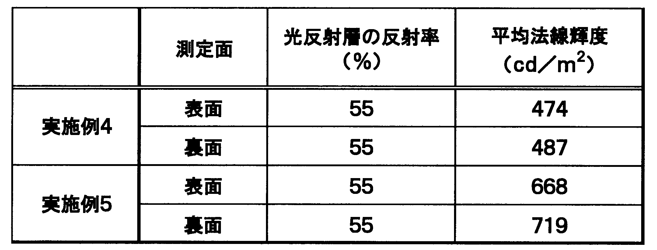
- Table 2 shows the average normal luminance of the light source device 60 obtained.
- the surface refers to the surface of the light reflecting layer 14 laminated on the first cladding layer 121 that faces the interface between the light reflecting layer 14 and the adhesive layer 13.
- the back surface refers to the surface of the light reflecting layer 14 laminated on the second cladding layer 122 that faces the interface between the light reflecting layer 14 and the adhesive layer 13.
- Example 5 Except that the distance L between the light emitting means 15 is in the range of 0.2 to 1.0 mm, and the distance L between the light emitting means 15 is reduced in proportion to the distance from the light incident surface 16.
- the light source device 60 was obtained by performing the same operation as in Example 4.
- Table 2 shows the reflectance of the light reflection layer 14 and the average normal luminance of the obtained light source device 60.
- a light source device can be obtained in a simple process. Further, the obtained light source device was excellent in luminance, and the luminance of the light source device could be controlled according to the reflectance of the light reflecting layer 14.
- the laminate of the present invention is easy to adjust the reflectance of the light reflecting layer and has excellent durability. Further, by using the laminate of the present invention, a light source device having excellent luminance can be obtained.
- the obtained light source device is, for example, a backlight key of a mobile phone, a backlight keyboard of a personal computer, a display of an electric device or a vehicle as a light source device of a liquid crystal display device used in a mobile phone, a notebook computer, a liquid crystal television, a video camera, etc.
- a light source device of a display device such as a switch, it can be suitably used as a light source device such as a room light such as a ceiling light or an illumination device such as an illumination signboard.
Landscapes
- Physics & Mathematics (AREA)
- General Physics & Mathematics (AREA)
- Optics & Photonics (AREA)
- Engineering & Computer Science (AREA)
- Manufacturing & Machinery (AREA)
- Planar Illumination Modules (AREA)
- Laminated Bodies (AREA)
Abstract
Description
本願は、2013年6月18日に日本に出願された特願2013-127273号、及び2013年8月7日に日本に出願された特願2013-163827号に基づき優先権を主張し、その内容をここに援用する。
特許文献1で提案されている光源装置用導光体は、印刷により光反射層を形成しているため、光反射層の厚さに斑が生じて反射率のばらつきが起こりやすく、したがって導光体の輝度に斑が生じやすい。
また、印刷による光反射層の形成では、1回の印刷工程で高い反射率を得ることが困難である。高い反射率を得るためには、印刷工程を複数回繰り返し、光反射層の厚さを厚くする必要がある。その結果、工程が煩雑となり、加工コストが上昇する。更に、導光体を屈曲した場合、印刷により形成した光反射層は剥離しやすく、光反射層の耐久性は十分ではない。
また、本発明の目的は、反射率の調整が簡便で耐久性に優れる光反射層を備えた積層体の、簡便かつ加工コストが抑制された製造方法を提供することにある。
更に、反射率の調整が簡便で耐久性に優れる光反射層を備えた積層体を有する、輝度に優れる光源装置を提供することにある。
(1)コア層と、第1クラッド層と、第2クラッド層と、光反射層とを有する積層体であって、前記光反射層、前記第2クラッド層、前記コア層及び前記第1クラッド層は順次積層されており、前記第1クラッド層の屈折率及び前記第2クラッド層の屈折率が前記コア層の屈折率よりも低く、前記光反射層の厚さが50μm以上である積層体。
(2)更に、光出射手段を有する、(1)に記載の積層体。
(3)前記光反射層と前記第2クラッド層との間に、更に粘着層を含む、(1)又は(2)に記載の積層体。
(4)前記光反射層が、光を散乱反射させる材料で構成されている、(1)~(3)のいずれか1つに記載の積層体。
(5)前記光反射層の材料が、ポリオレフィン樹脂、ポリエステル樹脂、アクリル樹脂及びセルロースからなる群より選択される少なくとも1種の材料である、(1)~(4)のいずれか1つに記載の積層体。
(6)前記光反射層の反射率が、70%以上である、(1)~(5)のいずれか1つに記載の積層体。
(7)前記光反射層の反射率が、65%以下である、(1)~(5)のいずれか1つに記載の積層体。
(8)前記光反射層において、前記光反射層と第2クラッド層との界面に対向する面に、更に意匠層及び光拡散層からなる群より選択される少なくとも1種の層が積層されている、(7)に記載の積層体。
(9)コア層の第1面に第1クラッド層を積層すること、コア層の第2面に第2クラッド層を積層すること、及び前記第2クラッド層の第2面に光反射層を積層することを含む積層体の製造方法であって、前記第1クラッド層の屈折率及び前記第2クラッド層の屈折率が前記コア層の屈折率よりも低く、前記光反射層の厚さが50μm以上であり、前記光反射層の積層がラミネーションにより行われる製造方法。
(10)(1)~(8)のいずれか1つに記載の積層体を含む、光源装置用導光体。
(11)(1)~(8)のいずれか1つに記載の積層体及び光源を有する、光源装置。
(12)(6)に記載の積層体及び光源を有する、片面発光光源装置。
(13)(7)又は(8)に記載の積層体及び光源を有する、両面発光光源装置。
本発明の積層体の製造方法によれば、反射率の調整が簡便で耐久性に優れた光反射層を備えた積層体を簡便に、加工コストを抑制して形成することができる。また、得られる積層体を用いることで輝度に優れる光源装置が得られる。
本発明の光源装置は、反射率の調整が簡便で耐久性に優れる光反射層を備えた積層体を有し、輝度に優れる。
本発明の一態様である積層体10(以下、単に本発明の積層体10と言うことがある)は、コア層11と、第1クラッド層121と、第2クラッド層122と、光反射層14とを有する積層体であって、前記光反射層14、前記第2クラッド層122、前記コア層11及び前記第1クラッド層121はこの記載順で下側から順次積層されており、前記第1クラッド層121の屈折率及び前記第2クラッド層122の屈折率が前記コア層11の屈折率よりも低く、第2クラッド層122と光反射層14との間に更に粘着層13を含む。
図1は、本発明の積層体10の一実施形態を示す模式的斜視図である。図1に示す積層体10は、コア層11と、第1クラッド層121と、第2クラッド層122と、光反射層14とを有し、第2クラッド層122と光反射層14との間に更に粘着層13を含む。
積層体10は、その全体が湾曲又は屈曲した形状であってもよい。
コア層11は、透明性の高い材料で構成されていれば特に限定されず、使用目的等に応じて適宜選択することができる。透明性が高いとは、ISO 13468に準拠して測定した透過率の値が50~100%であることを言う。
コア層11の材料としては、例えば、アクリル樹脂、ポリカーボネート樹脂、脂環式ポリオレフィン樹脂、ガラス等が挙げられる。これらのコア層11の材料の中でも、軽量で取り扱い性に優れることから、アクリル樹脂、ポリカーボネート樹脂、脂環式ポリオレフィン樹脂が好ましい。
アクリル樹脂としては、例えば、メチルメタクリレート単独重合体、メチルメタクリレートと他の単量体との共重合体等が挙げられる。これらのアクリル樹脂の中でも、より透明性、耐久性に優れ、より安価であることから、メチルメタクリレート単独重合体、メチルメタクリレート単位を共重合体の総質量に対して50質量%以上100%未満含む共重合体が好ましい。
メチルメタクリレートと他の単量体との共重合体を用いる場合、共重合体中のメチルメタクリレート単位の含有率は、共重合体の総質量に対して50質量%以上100%未満が好ましく、60質量%以上100%未満がより好ましく、70質量%以上100%未満が更に好ましい。
他の単量体としては、例えば、メチルアクリレート、エチル(メタ)アクリレート、n-プロピル(メタ)アクリレート、n-ブチル(メタ)アクリレート、n-ヘキシル(メタ)アクリレート、シクロヘキシル(メタ)アクリレート等の(メタ)アクリレート類;(メタ)アクリル酸;無水マレイン酸;マレイミド類;スチレン等の芳香族ビニル類等が挙げられる。
尚、本明細書において、(メタ)アクリレートとは、アクリレート又はメタクリレートをいう。
尚、開口数とは、光を集める指標のことであり、開口数が大きいほど受光量を増やすことができ、積層体10を屈曲しても漏光を低く抑えることができる。
第1クラッド層121、第2クラッド層122は、透明性の高い材料で、コア層11の屈折率よりも屈折率が低い材料で構成されていれば特に限定されず、使用目的等に応じて適宜選択することができる。
第1クラッド層121、第2クラッド層122の材料は、コア層11の屈折率よりも屈折率が低い材料を適宜選択することができる。
フッ素含有オレフィン樹脂としては、例えば、フッ化ビニリデン単独重合体、フッ化ビニリデンとテトラフルオロエチレンとの共重合体、フッ化ビニリデンとヘキサフルオロプロピレンとの共重合体、フッ化ビニリデンとトリフルオロエチレンとの共重合体、フッ化ビニリデンとテトラフルオロエチレンとヘキサフルオロプロピレンとの共重合体等が挙げられる。これらのフッ素含有オレフィン樹脂の中でも、加工性や成形性に優れることから、フッ化ビニリデン単独重合体が好ましい。
フッ素含有オレフィン樹脂、アクリル樹脂の具体例は、前述と同様で、好ましい範囲と理由も、前述と同様である。
尚、コア層11の屈折率n1と第1クラッド層121及び/又は第2クラッド層122の屈折率n2との屈折率差は、コア層11の屈折率n1から第1クラッド層121及び/又は第2クラッド層122の屈折率n2を引いた値とする。
屈折率は、ISO 13468に準拠し、23℃でナトリウムD線を用いてアッベ屈折計にて測定した値とする。
第1クラッド層121の厚さは、第1クラッド層121の鉛直方向に切断した断面を顕微鏡にて撮影し、第1クラッド層121の第2面の任意の点から第1クラッド層121の第1面までの最短の寸法を任意の5箇所測定し(但し、光出射手段15を設けていない部分とする。)、その平均値を求めることにより算出する。第2クラッド層122の厚さは、第2クラッド層122の鉛直方向に切断した断面を顕微鏡にて撮影し、第2クラッド層122の第2面の任意の点から第2クラッド層122の第1面までの最短の寸法を任意の5箇所測定し(但し、光出射手段15を設けていない部分とする。)、その平均値を求めることにより算出する。
コア層11の体積と第1クラッド層121の体積との比率、コア層11の体積と第2クラッド層122の体積との比率は、コア層11の材料と第1クラッド層121及び第2クラッド層122の材料に応じて適宜選択することができる。
粘着層13は、第1クラッド層121及び第2クラッド層122と光反射層14とを密着させる役割を有する。
粘着層13は、透明性の高い材料で、第1クラッド層121及び第2クラッド層122と光反射層14に対して密着性に優れる材料であれば、使用目的等に応じて適宜選択することができる。
粘着層13の材料としては、例えば、アクリル系粘着剤、天然ゴム系粘着剤、合成ゴム系粘着剤、シリコーン系粘着剤、ウレタン系粘着剤、エポキシ系粘着剤等が挙げられる。これらの粘着剤13は、1種を用いてもよく、2種以上を併用又は混合してもよい。これらの粘着剤13の中でも、密着性に優れることから、アクリル系粘着剤、天然ゴム系粘着剤、合成ゴム系粘着剤、シリコーン系粘着剤、ウレタン系粘着剤、エポキシ系粘着剤が好ましく、アクリル系粘着剤、天然ゴム系粘着剤、合成ゴム系粘着剤がより好ましく、アクリル系粘着剤が更に好ましい。
粘着層13の厚さは、粘着層13の鉛直方向に切断した断面を顕微鏡にて撮影し、粘着層13において、粘着層13と第1クラッド層121又は第2クラッド層122との界面に対向する面の任意の点から、粘着層13と第1クラッド層121又は第2クラッド層122との界面までの最短の寸法を任意の5箇所測定し(但し、光出射手段15を設けていない部分とする。)、その平均値を求めることにより算出する。
光反射層14は、光を散乱反射させることができる層であれば特に限定されず、使用目的等に応じて適宜選択することができる。
光反射層14の材料としては、例えば、ポリオレフィン樹脂、ポリエステル樹脂、アクリル樹脂等の樹脂板や樹脂フィルム;セルロース等の紙等が挙げられる。これらの光反射層14の材料の中でも、積層体10を屈曲しても光反射層14が剥離することが少なく、積層体10の耐久性に優れ、積層体10の保護フィルムとして兼ねることができることから、ポリオレフィン樹脂、ポリエステル樹脂、アクリル樹脂、セルロースが好ましく、ポリエステル樹脂がより好ましい。
顔料としては、例えば、酸化チタン、硫酸バリウム、炭酸カルシウム、炭酸マグネシウム等の白色顔料等が挙げられる。これらの顔料は、1種を単独で用いてもよく、2種以上を併用又は混合してもよい。これらの顔料の中でも、可視光の全領域に対して反射率が高いことから、白色顔料が好ましい。
光源装置60の片面のみを発光させる場合、光源装置60の輝度に優れることから、光反射層14の反射率は、70%以上が好ましく、70~100%がより好ましく、75~100%が更に好ましい。
光源装置60の両面を発光させる場合、光源装置60の両面の輝度のバランスをとり易くするため、光反射層14の反射率は、65%以下が好ましく、25~65%がより好ましく、30~60%以下が更に好ましい。
本明細書における反射率は、分光測色計を用いて、積層体10の光反射層14が形成されていない面、若しくは光反射層14の粘着層13が設けられている面から、560nmの光を照射し、560nmの光の反射率を測定することにより算出することができる。
光源装置60の第1面のみを発光させたい場合、光反射層14は、光源装置60の輝度に優れることから、積層体10の第2面のみに設けられることが好ましい。
光源装置60の両面を発光させたい場合、光反射層14は、積層体10の片面のみに設けられてもよく、積層体10の両面に設けられてもよい。
光反射層14が第1クラッド層121及び/又は第2クラッド層122の一部の領域を覆う場合、粘着層13は、光反射層14が設けられる領域のみに設けられてもよく、光反射層14が設けられていない領域を含めて設けられてもよい。
光反射層14が第2クラッド層122の一部の領域を覆う場合、その領域において光が反射するので、その領域に光出射手段15を設ける又は第1クラッド層のその領域に対向する領域に光出射手段15を設けることが好ましい。
図2は、本発明の一態様である積層体20(以下、単に本発明の積層体20と言うことがある)の一実施形態を示す模式的斜視図である。本発明の積層体20は、図2に示すように、更に光出射手段15を有することが好ましい。
図2に示す積層体20は、コア層11と、コア層11の第1面に設けられた第1クラッド層121と、コア層11の第2面に設けられた第2クラッド層122とを有し、第2クラッド層122の第2面に粘着層13を介して光反射層14が設けられ、第1クラッド層121に、その第1面からコア層11の内部まで達する光出射手段15が設けられている。
図3は、光反射層14を設けていない積層体の一形態を示す模式的断面図である。図3に示す積層体は、コア層11と、コア層11の第1面に設けられた第1クラッド層121と、コア層11の第2面に設けられた第2クラッド層122とを有し、第1クラッド層121に、その第1面からコア層11の内部に達する光出射手段15が設けられている。
光源装置60の片面のみを発光させたい場合、光出射手段15は、積層体30の片面のみに設けられてもよく、積層体30の両面に設けられてもよい。
光源装置60の両面を発光させたい場合、光出射手段15は、光源装置60の両面の輝度の調整が容易であることから、積層体30の両面に設けられることが好ましい。
光出射手段15の形状としては、円錐形状、角錐形状、球欠形状、三角柱、四角柱等の角柱形状、ライン形状等が挙げられる。これらの形状の光出射手段15は、1種を単独で用いてもよく、2種以上を併用してもよい。
光出射手段15の形状が円錐形状、角錐形状、球欠形状の場合、円錐形、角錐形、球欠形状の底面は、光出射手段15が設けられている面に存在する。
光出射手段15の形状が角柱形状の場合、角柱の長手方向は、積層体30の光入射面の法線方向(導光方向ともいう)と平行であってもよいし、積層体30の光入射面の法線方向と垂直に交わるものであってもよいし、積層体30の光入射面の法線方向と任意の角度で斜めに交わるものであってもよい。また、光出射手段15の形状がコア層11の第1面の法線方向上側から見て円状のラインである場合、複数の光出射手段15が同心円状に配置したものでもよい。
光出射手段15の深さDは、第1クラッド層121を貫通してコア層11の内部に達し、コア層11を貫通しない深さであることが好ましい。即ち、光出射手段15の深さDと、第1クラッド層121の厚さd1、コア層11の厚さd11とで、d1<D<d1+d11を満たすことが好ましい。光出射手段15の大きさが前記範囲であると、コア層11内を伝播してきた光を十分にコア層11から取り出すことができる。尚、光出射手段15の深さDは、光出射面17から光出射手段15の最深部までの距離を表すものとする。
光出射手段15の深さDは、0.1~1000μmが好ましく、0.5~500μmがより好ましい。
光出射手段15の幅Wは、コア層11、第1クラッド層121、第2クラッド層122、光反射層14の材料に応じて適宜選択すればよい。尚、光出射手段15の幅Wは、光出射手段15の積層体30の光入射面の法線方向の最大幅広さを表すものとする。光出射手段15の深さD及び幅Wは、顕微鏡にて光出射手段15が設けられた積層体30を撮影し、任意に抽出した5箇所について深さD及び幅Wについて測定し、平均値を求めることにより算出することができる。
光出射手段15の幅Wは、1~10000μmが好ましく、5~5000μmがより好ましい。
例えば、光入射面16からの距離の長短にかかわらず、均一な輝度を有する光源装置60得るためには、光入射面16から離れるに従って、光出射手段15の深さDが大きくなるように光出射手段15を設けることが好ましい。即ち、図5に示すように、光出射手段15の深さD1~D4について、D1<D2<D3<D4を満たすことが好ましい。
例えば、均一な輝度の光源装置60を得るためには、光入射面16から離れるに従って、光出射手段15間の間隔L1、L2、L3が小さくなるように光出射手段15を設けることが好ましい。即ち、図5に示すように、光出射手段15間の間隔L1~L3について、L1>L2>L3を満たすことが好ましい。
光出射手段15の間の間隔Lは、光出射手段15の最深部と隣り合う光出射手段間15の最深部との間の最短の距離を表すものとする。光出射手段15の間の間隔Lは、顕微鏡にて光出射手段15が設けられた積層体40を撮影し、任意に抽出した5箇所について間隔Lについて測定し、平均値を求めることにより算出することができる。
光出射手段15間の間隔Lは、1~10000μmが好ましく、5~5000μmがより好ましい。
一般的な導光体は、工程内や輸送時の傷付防止のため、その表面に保護フィルムを設ける必要がある。傷付防止のような保護フィルムとしての機能を有する光反射層14を設けることで、光反射層14が設けられている積層体10、20、30、40の面に別途保護フィルムを設ける必要がなく、好ましい。
本発明の積層体10は、コア層11の第1面に第1クラッド層121を積層し、コア層11の第2面に第2クラッド層122を積層し、第2クラッド層122の第2面に粘着層13を介して光反射層14を積層して得ることができる。粘着層13を介して第2クラッド層122に光反射層14が積層されているとは、粘着層13が第2クラッド層122と光反射層14の間に存在することを言う。
コア層11の第1面に第1クラッド層121を積層する工程と、コア層11の第2面に第2クラッド層122を積層する工程とは、同時に行われてもよく、別々に行われてもよく、また、どちらが先に行われてもよい。
本発明の積層体の製造方法によれば、反射率の調整が簡便で耐久性に優れた光反射層を備えた積層体を簡便に、加工コストを抑制して形成することができる。
コーティング処理の方法としては、例えば、ダイコート法、グラビアコート法、スピンコート法、ディップコート法、バーコート法、スプレーコート法、印刷法等が挙げられる。
印刷処理の方法としては、例えば、スクリーン印刷法、インクジェット印刷法等が挙げられる。
コーティング処理の方法としては、前述した方法が挙げられる。
コーティング処理の方法としては、前述した方法が挙げられる。
ラミネーションとは、貼り付けることを意味する。
積層体20、30、40に光出射手段15を設ける方法としては、例えば、レーザー加工、サンドペーパー加工、プレス加工、熱プレス加工等が挙げられる。
光源装置60の片面のみを発光させたい場合、意匠層又は光拡散層18は、積層体20、30、40の光出射面17に設けられることが好ましい。
光源装置60の両面を発光させたい場合、意匠層又は光拡散層18は、積層体20、30、40の両面に設けられることが好ましい。
意匠層又は光拡散層18は、積層体20、30、40の面の一部を覆っていてもよく、全部を覆っていてもよい。
意匠層又は光拡散層18の上に、更に意匠層又は光拡散層を設けてもよい。この場合、光拡散層の上に意匠層が設けられることが好ましい。
コーティング処理の方法としては、前述した方法が挙げられる。
印刷処理の方法としては、前述した方法が挙げられる。
本発明の積層体10、20、30、40、50(以下、10~50と表すことがある)は、光源装置用導光体10、20、30、40、50(以下、10~50と表すことがある)として用いることができる。
光源装置用導光体10~50としては、光源装置60の輝度を制御することができることから、光出射手段15を有する本発明の積層体20、30、40、50を用いることが好ましい。
本発明の積層体を光源装置用導光体として用いることで、光源装置60を得ることができる。
図7は、本発明の積層体10~50を用いた光源装置60の一実施形態を示す模式的断面図である。図7に示す光源装置60は、本発明の積層体10~50を光源装置用導光体10~50として用い、光入射面16側に光源31を、光出射面17側に意匠層又は光拡散層18が設けられている。
意匠層又は光拡散層18は、光源装置用導光体10~50と離間してもよく、粘着層19等を介して密着してもよいが、光源装置60を薄型化でき、製造コストを抑制することができることから、粘着層19等を介して密着することが好ましい。
粘着層19は、前述した粘着層13と同様のものを用いることができる。
実施例で用いた片面に粘着層13が設けられている光反射層14について、分光測色計(機種名「CM-508d」、コニカミノルタ(株)製)を用い、粘着層13が設けられている面から、560nmの光の反射率を測定した。得られた反射率を、光反射層14の反射率とした。
実施例で得られた光出射手段15を設ける前の積層体10について、分光測色計(機種名「CM-508d」、コニカミノルタ(株)製)を用い、積層体10の光反射層14が形成されていない側の面から、560nmの光の反射率を測定した。得られた反射率を、積層体10の反射率とした。
実施例で得られた積層体の光出射手段15について、レーザー共焦点顕微鏡(機種名「LEXT OLS-3000」、オリンパス(株)製)を用い、任意に抽出した3箇所について、深さD及び幅Wを測定し、その平均値を光出射手段15の深さD及び幅Wとした。
実施例で得られた光源装置60について、図8に示すような測定装置を用い、平均法線輝度を測定した。
実施例1~3で得られた光源装置60については、以下のように平均法線輝度を測定した。
両端に光源31として配置したLEDをそれぞれ67mAで発光させ、輝度計70(機種名「BM-7A」、(株)トプコンテクノハウス製)を用い、光入射面16から10mmの位置から210mmの位置までの領域について、10mm刻みで21点の法線方向の輝度を光出射面17から500mmの高さから測定し、その平均値を平均法線輝度とした。尚、輝度測定における視野角は、2°とした。
実施例4~5で得られた光源装置60については、以下のように平均法線輝度を測定した。
片端に光源31として配置したLEDをそれぞれ67mAで発光させ、輝度計70(機種名「BM-7A」、(株)トプコンテクノハウス製)を用い、光入射面16から20mmの位置から280mmの位置までの領域について、10mm刻みで27点の法線方向の輝度を光出射面17から500mmの高さから測定し、その平均値を平均法線輝度とした。尚、輝度測定における視野角は、2°とした。
実施例で得られた光源装置60について、図9に示すような測定装置を用い、輝度分布を測定した。
光源31として配置したLEDをそれぞれ67mAで発光させ、輝度計70(機種名「BM-7A」、(株)トプコンテクノハウス製)を用い、光源装置用導光体の中央の位置を中心とした8mm四方のエリアの光出射面17から出射される光の、導光方向と平行で光出射面に垂直な面の-80°から80°までの出射角度における輝度分布を光出射面17から500mmの高さから測定した。
尚、光の出射方向は、光出射面17に対して法線方向を0°、一方の光入射面16を-(マイナス)、その反対の光入射面16を+(プラス)とし、各出射角度での輝度値は、ピーク輝度の値を1として規格化した相対輝度とした。
実施例で得られた光出射手段15を設ける前の積層体10について、ISO 179に準拠して、積層体10の反射層14が形成された面に20kg重の重りにより衝撃を与え、シャルピー衝撃強度を測定した。
コア層11の材料としてポリカーボネート樹脂(商品名「タフロン LC2200」、出光興産(株)製、屈折率n1=1.585)、第1クラッド層121及び第2クラッド層122の材料としてアクリル樹脂(商品名「アクリペット VH000」、三菱レイヨン(株)製、屈折率n2=1.49)を用い、多層溶融押出により第1クラッド層121及び第2クラッド層122の厚さがそれぞれ20μm、全体の厚さが0.7mmの積層体10を得た。第2クラッド層122の表面に、片面に粘着層13が設けられている光反射層14(商品名「B310W」(商品名、(株)サンエー化研製、ポリエチレンテレフタレート、白色フィルム)の粘着層13側の面をラミネーションした。光反射層14の厚さは65μm、粘着層の厚さは4μmであった。積層体10の反射率を測定した。
得られた積層体10を幅50mm、長さ420mmの矩形に切断し、4つの側面が鏡面となるようにダイヤモンドバイトにより切削した。次いで、第1クラッド層121の第1面、すなわち光出射面17となる面に、炭酸ガスレーザー加工装置(機種名「PLS6.120D」、ユニバーサルレーザーシステム社製)を用い、レーザー照射加工を施し、略円錐の凹部の光出射手段15を形成し、積層体40を得た。尚、レーザー照射のパターンは、光出射手段15間の間隔Lを0.4~1.2mmの範囲内とし、光入射面16から離れるに比例して、光出射手段15間の間隔Lが小さくなるようにした。また、光出射手段15は、いずれも深さDが60μm、幅(直径)Wが166μmであった。
得られた積層体40を光源装置用導光体として用い、光源装置用導光体の2つの対向する側面を光入射面16とし、光源装置用導光体の2つの対向する側面である光入射面16と対向するように、光源31としてLED(白色チップLED、商品名「NSSW157T」、日亜化学工業(株)製)をそれぞれの光入射面16に対してLEDの中心間の距離が10mmとなるように5個配置し、光源装置60を得た。得られた光源装置60の平均法線輝度を表1に、得られた光源装置60の輝度分布を図10に示す。
片面に粘着層13が設けられている光反射層14を「E-241 WS」(商品名、(株)スミロン製、ポリエチレンテレフタレート、白色フィルム)に変更した以外は、実施例1と同様に操作を行い、光源装置60を得た。光反射層14の厚さ、光反射層14の反射率、積層体10の反射率、得られた光源装置60の平均法線輝度を表1に、得られた光源装置60の輝度分布を図11に示す。また、粘着層の厚さは4μmであった。
片面に粘着層13が設けられている光反射層14を「MTN-W400」(商品名、(株)ツジデン製、ポリエチレンテレフタレート、白色フィルム)に変更した以外は、実施例1と同様に操作を行い、光源装置60を得た。光反射層の厚さ、光反射層14の反射率、積層体10の反射率、得られた光源装置60の平均法線輝度を表1に、得られた光源装置60の輝度分布を図12に示す。また、粘着層の厚さは4μmであった。
片面に粘着層13が設けられている光反射層14をラミネーションする代わりに、白色のスクリーン印刷インキ(商品名「#2500 120ホワイト」、(株)セイコーアドバンス製、アクリル樹脂)を用い、スクリーン印刷を1回行った以外は、実施例1と同様に操作を行い、光源装置60を得た。光反射層の厚さ、積層体10の反射率、得られた光源装置60の平均法線輝度を表1に示す。
[比較例2]
スクリーン印刷を3回とした以外は、比較例1と同様に操作を行い、光源装置60を得た。光反射層の厚さ、積層体10の反射率、得られた光源装置60の平均法線輝度を表1に示す。

コア層11の材料としてポリカーボネート樹脂(商品名「タフロン LC2200」、出光興産(株)製、屈折率n1=1.585)、第1クラッド層121及び第2クラッド層122の材料としてアクリル樹脂(商品名「アクリペット VH000」、三菱レイヨン(株)製、屈折率n2=1.49)を用い、多層溶融押出により第1クラッド層121及び第2クラッド層122の厚さがそれぞれ20μm、全体の厚さが0.7mmの積層体を得た。
得られた積層体10を幅50mm、長さ300mmの矩形に切断し、4つの側面が鏡面となるようにダイヤモンドバイトにより切削した。次いで、得られた積層体10の第1クラッド層121及び第2クラッド層122の表面に、炭酸ガスレーザー加工装置(機種名「PLS6.120D」、ユニバーサルレーザーシステム社製)を用い、レーザー照射加工を施し、略円錐の凹部の光出射手段15を形成し、積層体40を得た。尚、レーザー照射のパターンは、光出射手段15間の間隔Lを0.4~1.2mmの範囲内とし、光入射面16からの距離に比例して、光出射手段15間の間隔Lが小さくなるようにした。また、光出射手段15は、深さDが60μm、幅(直径)Wが166μmであった。
得られた積層体の第1クラッド層121の第1面及び第2クラッド層122の第2面に、片面に粘着層13が設けられている光反射層14(商品名「FM-715W」、大王加工紙工業(株)製、白色フィルム)の粘着層13を有する面をラミネーションした。光反射層14の厚さは70μm、粘着層の厚さは4μmであった。
得られた積層体を光源装置用導光体として用い、光源装置用導光体の2つの対向する側面の一方を光入射面16とし、光入射面16と対向するように光源31としてLED(商品名「NSSW157T」、日亜化学工業(株)製)をLEDの中心間の距離が10mmとなるように5個配置し、両面発光する光源装置60を得た。得られた光源装置60の平均法線輝度を表2に示す。なお、表2において表面とは、第1クラッド層121にラミネーションされた光反射層14において、光反射層14と粘着層13の界面と対向する面を言う。また、表2において裏面とは、第2クラッド層122にラミネーションされた光反射層14において、光反射層14と粘着層13との界面と対向する面を言う。
光出射手段15間の間隔Lを0.2~1.0mmの範囲内とし、光入射面16からの距離に比例して、光出射手段15間の間隔Lが小さくなるようにした以外は、実施例4と同様に操作を行い、光源装置60を得た。光反射層14の反射率、得られた光源装置60の平均法線輝度を表2に示す。
11 コア層
121 第1クラッド層
122 第2クラッド層
13 粘着層
14 光反射層
15 光出射手段
15a 光出射手段
15b 光出射手段
15c 光出射手段
15d 光出射手段
16 光入射面
17 光出射面
18 意匠層又は光拡散層
19 粘着層
10、20、30、40、50 光源装置用導光体
60 光源装置
31 光源
70 輝度計
Claims (13)
- コア層と、第1クラッド層と、第2クラッド層と、光反射層とを有する積層体であって、前記光反射層、前記第2クラッド層、前記コア層及び前記第1クラッド層は順次積層されており、前記第1クラッド層の屈折率及び前記第2クラッド層の屈折率が前記コア層の屈折率よりも低く、前記光反射層の厚さが50μm以上である積層体。
- 更に、光出射手段を有する、請求項1に記載の積層体。
- 前記光反射層と前記第2クラッド層との間に、更に粘着層を含む、請求項1又は2に記載の積層体。
- 前記光反射層が、光を散乱反射させる材料で構成されている、請求項1~3のいずれか1項に記載の積層体。
- 前記光反射層の材料が、ポリオレフィン樹脂、ポリエステル樹脂、アクリル樹脂及びセルロースからなる群より選択される少なくとも1種の材料である、請求項1~4のいずれか1項に記載の積層体。
- 前記光反射層の反射率が、70%以上である、請求項1~5のいずれか1項に記載の積層体。
- 前記光反射層の反射率が、65%以下である、請求項1~5のいずれか1項に記載の積層体。
- 前記光反射層において、前記光反射層と第2クラッド層との界面に対向する面に、更に意匠層及び光拡散層からなる群より選択される少なくとも1種の層が積層されている、請求項7に記載の積層体。
- コア層の第1面に第1クラッド層を積層すること、コア層の第2面に第2クラッド層を積層すること、及び前記第2クラッド層の第2面に光反射層を積層することを含む積層体の製造方法であって、前記第1クラッド層の屈折率及び前記第2クラッド層の屈折率が前記コア層の屈折率よりも低く、前記光反射層の厚さが50μm以上であり、前記光反射層の積層がラミネーションにより行われる製造方法。
- 請求項1~8のいずれか1項に記載の積層体を含む、光源装置用導光体。
- 請求項1~8のいずれか1項に記載の積層体及び光源を有する、光源装置。
- 請求項6に記載の積層体及び光源を有する、片面発光光源装置。
- 請求項7又は8に記載の積層体及び光源を有する、両面発光光源装置。
Priority Applications (4)
| Application Number | Priority Date | Filing Date | Title |
|---|---|---|---|
| CN201480033961.0A CN105324606A (zh) | 2013-06-18 | 2014-06-16 | 叠层体、叠层体的制造方法、光源装置用导光体及光源装置 |
| JP2014532130A JPWO2014203850A1 (ja) | 2013-06-18 | 2014-06-16 | 積層体、積層体の製造方法、光源装置用導光体及び光源装置 |
| US14/893,548 US20160139324A1 (en) | 2013-06-18 | 2014-06-16 | Laminate, method for producing laminate, light guide body for light source devices, and light source device |
| KR1020157031777A KR20160021755A (ko) | 2013-06-18 | 2014-06-16 | 적층체, 적층체의 제조 방법, 광원 장치용 도광체 및 광원 장치 |
Applications Claiming Priority (4)
| Application Number | Priority Date | Filing Date | Title |
|---|---|---|---|
| JP2013127273 | 2013-06-18 | ||
| JP2013-127273 | 2013-06-18 | ||
| JP2013-163827 | 2013-08-07 | ||
| JP2013163827 | 2013-08-07 |
Publications (1)
| Publication Number | Publication Date |
|---|---|
| WO2014203850A1 true WO2014203850A1 (ja) | 2014-12-24 |
Family
ID=52104584
Family Applications (1)
| Application Number | Title | Priority Date | Filing Date |
|---|---|---|---|
| PCT/JP2014/065883 Ceased WO2014203850A1 (ja) | 2013-06-18 | 2014-06-16 | 積層体、積層体の製造方法、光源装置用導光体及び光源装置 |
Country Status (6)
| Country | Link |
|---|---|
| US (1) | US20160139324A1 (ja) |
| JP (1) | JPWO2014203850A1 (ja) |
| KR (1) | KR20160021755A (ja) |
| CN (1) | CN105324606A (ja) |
| TW (1) | TW201505847A (ja) |
| WO (1) | WO2014203850A1 (ja) |
Cited By (3)
| Publication number | Priority date | Publication date | Assignee | Title |
|---|---|---|---|---|
| WO2017053235A1 (en) * | 2015-09-25 | 2017-03-30 | Snaptrack, Inc. | Etendue-preserving light coupling system having light output aperture smaller than light input aperture |
| JP2023061257A (ja) * | 2021-10-19 | 2023-05-01 | パナソニックIpマネジメント株式会社 | 導光シート |
| WO2023181709A1 (ja) * | 2022-03-25 | 2023-09-28 | 日東電工株式会社 | 光学積層体 |
Families Citing this family (3)
| Publication number | Priority date | Publication date | Assignee | Title |
|---|---|---|---|---|
| CN106154401A (zh) * | 2015-04-27 | 2016-11-23 | 鸿富锦精密工业(深圳)有限公司 | 一种光纤导光装置及背光模组 |
| JP7485503B2 (ja) * | 2018-07-17 | 2024-05-16 | ツェット・エフ・オートモーティブ・ジャーマニー・ゲーエムベーハー | 積層体を評価する方法、積層体を評価する装置、積層体を製造する方法、及び積層体を製造する装置 |
| CN111447765B (zh) * | 2020-04-30 | 2021-03-23 | 京东方科技集团股份有限公司 | 壳体结构及电子设备 |
Citations (4)
| Publication number | Priority date | Publication date | Assignee | Title |
|---|---|---|---|---|
| JPH07110409A (ja) * | 1993-10-08 | 1995-04-25 | Mitsubishi Cable Ind Ltd | エッジ光源式平面ランプ用導光板 |
| WO2010073726A1 (ja) * | 2008-12-25 | 2010-07-01 | 三菱レイヨン株式会社 | 光源装置用導光体及びその製造方法 |
| JP2012156082A (ja) * | 2011-01-28 | 2012-08-16 | Furukawa Electric Co Ltd:The | バックライトパネル、導光板、反射板、および接着シート |
| JP2012212000A (ja) * | 2011-03-31 | 2012-11-01 | Furukawa Electric Co Ltd:The | 光反射板及びバックライトユニット |
Family Cites Families (5)
| Publication number | Priority date | Publication date | Assignee | Title |
|---|---|---|---|---|
| US6100943A (en) * | 1996-07-09 | 2000-08-08 | Harness System Technologies Research, Inc. | Vehicular display device for directly and indirectly displaying information |
| GB2336660B (en) * | 1998-04-20 | 2002-03-06 | Bridgestone Corp | Light transmission tubes and methods for manufacturing the light transmission tubes |
| US20010036546A1 (en) * | 1999-08-03 | 2001-11-01 | Kaytor Scott R. | Dimensionally stabilized diffuse reflective articles |
| US8480282B2 (en) * | 2005-08-30 | 2013-07-09 | Lg Display Co., Ltd. | Reflective plate and method for manufacturing the same and backlight unit for liquid crystal display device using the same |
| GB2478987A (en) * | 2010-03-26 | 2011-09-28 | Iti Scotland Ltd | Encapsulation of an LED array forming a light concentrator for use with edge-lit light-guided back lights |
-
2014
- 2014-06-16 JP JP2014532130A patent/JPWO2014203850A1/ja active Pending
- 2014-06-16 CN CN201480033961.0A patent/CN105324606A/zh active Pending
- 2014-06-16 WO PCT/JP2014/065883 patent/WO2014203850A1/ja not_active Ceased
- 2014-06-16 US US14/893,548 patent/US20160139324A1/en not_active Abandoned
- 2014-06-16 KR KR1020157031777A patent/KR20160021755A/ko not_active Withdrawn
- 2014-06-17 TW TW103120775A patent/TW201505847A/zh unknown
Patent Citations (4)
| Publication number | Priority date | Publication date | Assignee | Title |
|---|---|---|---|---|
| JPH07110409A (ja) * | 1993-10-08 | 1995-04-25 | Mitsubishi Cable Ind Ltd | エッジ光源式平面ランプ用導光板 |
| WO2010073726A1 (ja) * | 2008-12-25 | 2010-07-01 | 三菱レイヨン株式会社 | 光源装置用導光体及びその製造方法 |
| JP2012156082A (ja) * | 2011-01-28 | 2012-08-16 | Furukawa Electric Co Ltd:The | バックライトパネル、導光板、反射板、および接着シート |
| JP2012212000A (ja) * | 2011-03-31 | 2012-11-01 | Furukawa Electric Co Ltd:The | 光反射板及びバックライトユニット |
Cited By (6)
| Publication number | Priority date | Publication date | Assignee | Title |
|---|---|---|---|---|
| WO2017053235A1 (en) * | 2015-09-25 | 2017-03-30 | Snaptrack, Inc. | Etendue-preserving light coupling system having light output aperture smaller than light input aperture |
| US9823411B2 (en) | 2015-09-25 | 2017-11-21 | Snaptrack Inc. | Etendue-preserving light coupling system having light output aperture smaller than light input aperture |
| JP2023061257A (ja) * | 2021-10-19 | 2023-05-01 | パナソニックIpマネジメント株式会社 | 導光シート |
| WO2023181709A1 (ja) * | 2022-03-25 | 2023-09-28 | 日東電工株式会社 | 光学積層体 |
| JP2023142896A (ja) * | 2022-03-25 | 2023-10-06 | 日東電工株式会社 | 光学積層体 |
| US12541049B2 (en) | 2022-03-25 | 2026-02-03 | Nitto Denko Corporation | Optical layered body including cover sheets, pressure-sensitive adhesive layers, and light extraction layer |
Also Published As
| Publication number | Publication date |
|---|---|
| CN105324606A (zh) | 2016-02-10 |
| JPWO2014203850A1 (ja) | 2017-02-23 |
| KR20160021755A (ko) | 2016-02-26 |
| TW201505847A (zh) | 2015-02-16 |
| US20160139324A1 (en) | 2016-05-19 |
Similar Documents
| Publication | Publication Date | Title |
|---|---|---|
| TWI437292B (zh) | 光源裝置用導光體 | |
| JP2007304553A (ja) | プリズムシート、それを備えたバックライトユニット及び液晶表示装置 | |
| WO2014203850A1 (ja) | 積層体、積層体の製造方法、光源装置用導光体及び光源装置 | |
| JP2017107193A (ja) | 上用光拡散シート及びバックライトユニット | |
| JP2010262038A (ja) | 光偏向素子、及び拡散板 | |
| JP2010044270A (ja) | 光拡散板、光学シート、バックライトユニット及びディスプレイ装置 | |
| JP2008277025A (ja) | 面光源用光学シート、面光源装置及び表示装置 | |
| JP5104459B2 (ja) | 光学部材とそれを用いたバックライト・ユニット、ディスプレイ | |
| JP2010266611A (ja) | 光均一素子、光学シート、バックライトユニット及びディスプレイ装置 | |
| JP2010250987A (ja) | 光均一素子、光学シート、バックライトユニット及びディスプレイ装置 | |
| JP2010256431A (ja) | 積層樹脂シートとそれを用いたバックライトユニットおよびディスプレイ装置 | |
| JP2010044269A (ja) | 光拡散板、光学シート、バックライトユニット及びディスプレイ装置 | |
| WO2015020031A1 (ja) | 積層体の製造方法、積層体、光源装置用導光体及び光源装置 | |
| JP5327746B2 (ja) | 液晶表示装置 | |
| JP2008304700A (ja) | 光学シートおよび照明装置ならびに表示装置 | |
| JP2015032565A (ja) | 積層体、積層体の製造方法、光源装置用導光体及び光源装置 | |
| JP2017123218A (ja) | 導光体、導光体の製造方法及び光源装置 | |
| WO2012099123A1 (ja) | 導光板、面光源装置及び透過型画像表示装置 | |
| WO2012144451A1 (ja) | 照明装置および表示装置 | |
| JP2016096092A (ja) | 積層体及び積層体の製造方法 | |
| JP2010044268A (ja) | 光拡散板、光学シート、バックライトユニット及びディスプレイ装置 | |
| JP2016219121A (ja) | 面光源装置用導光体及び面光源装置 | |
| JP2018044994A (ja) | 表示装置 | |
| JP2015102578A (ja) | 看板用積層体及び看板 | |
| KR100878128B1 (ko) | 프리즘 시트 제조용 몰드 및 그 제조방법 |
Legal Events
| Date | Code | Title | Description |
|---|---|---|---|
| WWE | Wipo information: entry into national phase |
Ref document number: 201480033961.0 Country of ref document: CN |
|
| ENP | Entry into the national phase |
Ref document number: 2014532130 Country of ref document: JP Kind code of ref document: A |
|
| 121 | Ep: the epo has been informed by wipo that ep was designated in this application |
Ref document number: 14814318 Country of ref document: EP Kind code of ref document: A1 |
|
| ENP | Entry into the national phase |
Ref document number: 20157031777 Country of ref document: KR Kind code of ref document: A |
|
| WWE | Wipo information: entry into national phase |
Ref document number: 14893548 Country of ref document: US |
|
| NENP | Non-entry into the national phase |
Ref country code: DE |
|
| 122 | Ep: pct application non-entry in european phase |
Ref document number: 14814318 Country of ref document: EP Kind code of ref document: A1 |