WO2014188792A1 - Esd保護装置 - Google Patents
Esd保護装置 Download PDFInfo
- Publication number
- WO2014188792A1 WO2014188792A1 PCT/JP2014/059616 JP2014059616W WO2014188792A1 WO 2014188792 A1 WO2014188792 A1 WO 2014188792A1 JP 2014059616 W JP2014059616 W JP 2014059616W WO 2014188792 A1 WO2014188792 A1 WO 2014188792A1
- Authority
- WO
- WIPO (PCT)
- Prior art keywords
- discharge
- esd protection
- substrate
- electrode
- dielectric constant
- Prior art date
- Legal status (The legal status is an assumption and is not a legal conclusion. Google has not performed a legal analysis and makes no representation as to the accuracy of the status listed.)
- Ceased
Links
Images




Classifications
-
- H—ELECTRICITY
- H02—GENERATION; CONVERSION OR DISTRIBUTION OF ELECTRIC POWER
- H02H—EMERGENCY PROTECTIVE CIRCUIT ARRANGEMENTS
- H02H9/00—Emergency protective circuit arrangements for limiting excess current or voltage without disconnection
- H02H9/04—Emergency protective circuit arrangements for limiting excess current or voltage without disconnection responsive to excess voltage
-
- H—ELECTRICITY
- H01—ELECTRIC ELEMENTS
- H01T—SPARK GAPS; OVERVOLTAGE ARRESTERS USING SPARK GAPS; SPARKING PLUGS; CORONA DEVICES; GENERATING IONS TO BE INTRODUCED INTO NON-ENCLOSED GASES
- H01T1/00—Details of spark gaps
- H01T1/20—Means for starting arc or facilitating ignition of spark gap
- H01T1/22—Means for starting arc or facilitating ignition of spark gap by the shape or the composition of the electrodes
-
- H—ELECTRICITY
- H01—ELECTRIC ELEMENTS
- H01T—SPARK GAPS; OVERVOLTAGE ARRESTERS USING SPARK GAPS; SPARKING PLUGS; CORONA DEVICES; GENERATING IONS TO BE INTRODUCED INTO NON-ENCLOSED GASES
- H01T2/00—Spark gaps comprising auxiliary triggering means
- H01T2/02—Spark gaps comprising auxiliary triggering means comprising a trigger electrode or an auxiliary spark gap
-
- H—ELECTRICITY
- H01—ELECTRIC ELEMENTS
- H01T—SPARK GAPS; OVERVOLTAGE ARRESTERS USING SPARK GAPS; SPARKING PLUGS; CORONA DEVICES; GENERATING IONS TO BE INTRODUCED INTO NON-ENCLOSED GASES
- H01T4/00—Overvoltage arresters using spark gaps
- H01T4/10—Overvoltage arresters using spark gaps having a single gap or a plurality of gaps in parallel
-
- H—ELECTRICITY
- H10—SEMICONDUCTOR DEVICES; ELECTRIC SOLID-STATE DEVICES NOT OTHERWISE PROVIDED FOR
- H10W—GENERIC PACKAGES, INTERCONNECTIONS, CONNECTORS OR OTHER CONSTRUCTIONAL DETAILS OF DEVICES COVERED BY CLASS H10
- H10W42/00—Arrangements for protection of devices
- H10W42/60—Arrangements for protection of devices protecting against electrostatic charges or discharges, e.g. Faraday shields
-
- H—ELECTRICITY
- H10—SEMICONDUCTOR DEVICES; ELECTRIC SOLID-STATE DEVICES NOT OTHERWISE PROVIDED FOR
- H10W—GENERIC PACKAGES, INTERCONNECTIONS, CONNECTORS OR OTHER CONSTRUCTIONAL DETAILS OF DEVICES COVERED BY CLASS H10
- H10W70/00—Package substrates; Interposers; Redistribution layers [RDL]
- H10W70/60—Insulating or insulated package substrates; Interposers; Redistribution layers
- H10W70/62—Insulating or insulated package substrates; Interposers; Redistribution layers characterised by their interconnections
- H10W70/65—Shapes or dispositions of interconnections
-
- H—ELECTRICITY
- H10—SEMICONDUCTOR DEVICES; ELECTRIC SOLID-STATE DEVICES NOT OTHERWISE PROVIDED FOR
- H10W—GENERIC PACKAGES, INTERCONNECTIONS, CONNECTORS OR OTHER CONSTRUCTIONAL DETAILS OF DEVICES COVERED BY CLASS H10
- H10W70/00—Package substrates; Interposers; Redistribution layers [RDL]
- H10W70/60—Insulating or insulated package substrates; Interposers; Redistribution layers
- H10W70/67—Insulating or insulated package substrates; Interposers; Redistribution layers characterised by their insulating layers or insulating parts
- H10W70/68—Shapes or dispositions thereof
- H10W70/685—Shapes or dispositions thereof comprising multiple insulating layers
Definitions
- the present invention relates to an ESD protection device for protecting an electronic circuit from static electricity, and more particularly to an ESD protection device in which discharge electrodes are opposed to each other with a gap.
- Patent Document 1 discloses an ESD protection device in which first and second discharge electrodes are provided in a ceramic multilayer substrate. An auxiliary electrode is provided so as to be connected to the first and second discharge electrodes. The auxiliary electrode is formed by dispersing a conductive material coated with an inorganic material having no conductivity.
- Patent Document 2 discloses a chip-type surge absorber provided with discharge electrodes arranged opposite to each other via a discharge gap on an insulating substrate.
- a dielectric layer having a relative dielectric constant larger than that of the insulating substrate is provided between the discharge electrode and the insulating substrate. It is described that when the insulating substrate itself is formed of the dielectric layer, the capacitance increases and it is difficult to use it for a high-frequency circuit.
- the voltage is reduced by providing the dielectric layer.
- the dielectric layer is not provided in the discharge gap in order to prevent an increase in capacitance. That is, the dielectric layer is provided only directly below the discharge electrode on the insulating substrate. Accordingly, it is difficult to sufficiently use the creeping discharge among the air discharge and the creeping discharge. Therefore, it has been difficult to sufficiently lower the discharge start voltage.
- An object of the present invention is to provide an ESD protection device that can effectively lower a discharge start voltage.
- An ESD protection device includes a substrate, first and second discharge electrodes provided on the substrate and facing each other with a gap therebetween, and a high dielectric constant layer having a relative dielectric constant higher than that of the substrate. With.
- the high dielectric constant layer is provided so as to directly or indirectly connect the first discharge electrode and the second discharge electrode.
- the ESD protection device is preferably provided so as to connect the first discharge electrode and the second discharge electrode, and promotes discharge between the first and second discharge electrodes.
- a discharge auxiliary electrode is further provided.
- the discharge auxiliary electrode includes conductive particles coated with a material having no conductivity.
- the high dielectric constant layer is configured to be laminated on the discharge auxiliary electrode.
- the high dielectric constant layer is provided at least above or below the gap portion.
- a portion having a relative dielectric constant lower than that of the substrate is preferably located in the gap.
- a portion having a relative dielectric constant lower than that of the substrate may be a cavity.
- the portion having a relative dielectric constant lower than that of the substrate may be formed of a material having a relative dielectric constant lower than that of the substrate.
- a resin is used as the material having a relative dielectric constant lower than that of the substrate.
- the ESD protection device preferably further includes a back electrode provided so as to overlap with the gap between the first and second discharge electrodes via a part of the substrate.
- the substrate includes first and second external electrodes that are provided on the substrate and are electrically connected to the first and second discharge electrodes, respectively, and the back electrode includes the first and second electrodes. It is electrically connected to one of the external electrodes.
- the back electrode may be a floating electrode.
- the back electrode includes a metal and a material having a higher dielectric constant than the substrate.
- the first and second discharge electrodes may be disposed on the outer surface of the substrate.
- the tips of the first and second discharge electrodes may be disposed in the substrate, and the gap may be located in the substrate.
- the high dielectric constant layer having a higher relative dielectric constant than that of the substrate is directly or indirectly connected to the first and second discharge electrodes, so that the discharge start voltage can be lowered. Is possible. Therefore, it is possible to more effectively protect against static electricity in an electronic circuit or the like.
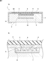
- FIG. 1A and FIG. 1B are a front sectional view of an ESD protection device according to a first embodiment of the present invention and a partially cutaway enlarged front sectional view for explaining the main part thereof.
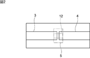
- FIG. 2 is a schematic plan view for explaining the positional relationship among the first and second discharge electrodes, the discharge auxiliary electrode, and the back electrode in the ESD protection apparatus according to the first embodiment of the present invention.
- FIG. 3A and FIG. 3B are a front sectional view of an ESD protection device according to a second embodiment of the present invention and a partially cutaway enlarged front sectional view showing an essential part thereof.
- FIG. 1A and FIG. 1B are a front sectional view of an ESD protection device according to a first embodiment of the present invention and a partially cutaway enlarged front sectional view for explaining the main part thereof.
- FIG. 2 is a schematic plan view for explaining the positional relationship among the first and second discharge electrodes, the discharge auxiliary electrode, and the back electrode in the ESD protection apparatus according to the first
- FIG. 4 is a schematic plan view showing the positional relationship among the first and second discharge electrodes, the discharge auxiliary electrode, and the back electrode in the second embodiment of the present invention.
- FIG. 5 is a schematic plan view for explaining a modification of the positional relationship among the first and second discharge electrodes, the discharge auxiliary electrode, and the back electrode.
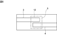
- FIG. 6 is a schematic plan view for explaining another modified example of the positional relationship among the first and second discharge electrodes, the discharge auxiliary electrode, and the back electrode.
- FIG. 7 is a front sectional view of an ESD protection apparatus according to the third embodiment of the present invention.
- FIG. 8 is a schematic plan view showing the positional relationship among the first and second discharge electrodes, the discharge auxiliary electrode, and the back electrode in the ESD protection apparatus according to the third embodiment of the present invention.
- FIG. 9 is a front sectional view of an ESD protection apparatus according to the fourth embodiment of the present invention.
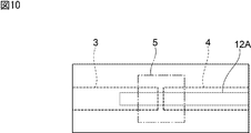
- FIG. 10 is a schematic plan view showing the positional relationship among the first and second discharge electrodes, the discharge auxiliary electrode, and the back electrode in the ESD protection apparatus according to the fourth embodiment of the present invention.
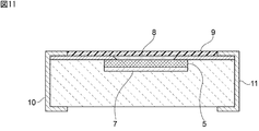
- FIG. 11 is a front sectional view of an ESD protection apparatus according to the fifth embodiment of the present invention.
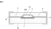
- FIG. 12 is a front sectional view of an ESD protection apparatus according to the sixth embodiment of the present invention.
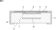
- FIG. 13 is front sectional drawing of the ESD protection apparatus which concerns on the 7th Embodiment of this invention.
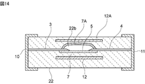
- FIG. 14 is a front sectional view of an ESD protection apparatus according to the eighth embodiment of the present invention.
- 1 (a) and 1 (b) are a front sectional view of an ESD protection device according to a first embodiment of the present invention and a partial cutaway front sectional view showing an essential part thereof.
- the ESD protection device 1 has a substrate 2.
- the substrate 2 is made of an appropriate insulating material.
- the substrate 2 is made of a ceramic multilayer substrate, and a BAS material containing Ba, Al, and Si as main components is used.
- LTCC low temperature sintered ceramics
- HTCC ceramics sintered at a high temperature such as aluminum nitride or alumina may be used.
- magnetic ceramics such as ferrite may be used.
- the relative dielectric constant of the substrate 2 is about 6 when the BAS material is used for the substrate, for example.
- the substrate 2 may be formed of an insulating material such as a resin other than ceramics.
- a first discharge electrode 3 and a second discharge electrode 4 are formed on the upper surface 2a of the substrate 2.
- a discharge auxiliary electrode 5 is provided on the lower surface of the first and second discharge electrodes 3 and 4 so as to connect the tips of the first and second discharge electrodes 3 and 4.
- the discharge auxiliary electrode 5 is provided on the upper surface 2 a of the substrate 2 so as to connect the first discharge electrode 3 and the second discharge electrode 4. As shown in FIG. 2, when viewed in plan, the discharge auxiliary electrode 5 is provided in a region including a gap region where the tips of the first and second discharge electrodes 3 and 4 are opposed to each other.
- the discharge auxiliary electrode 5 is formed by dispersing conductive particles 6 covered with a non-conductive material on the upper surface 2a of the substrate 2. More specifically, it is formed by applying and baking a paste containing such conductive particles. In this case, the coated conductive particles 6 that are not conductive and are contained in the paste are diffused from the upper surface 2 a of the substrate 2 to the surface layer of the substrate 2. As a result, the discharge auxiliary electrode is formed.
- the discharge auxiliary electrode 5 acts to promote the discharge between the tip of the first discharge electrode 3 and the tip of the second discharge electrode 4.
- the material constituting the conductive particles coated with the above non-conductive material is not particularly limited.
- the material having no electrical conductivity include insulating ceramics such as alumina, and glass.
- the material forming the conductive particles is not particularly limited, and a metal or the like can be used as appropriate.
- a metal copper or a copper-based alloy containing copper as a main component is preferably used.
- other metals such as silver, aluminum, molybdenum, tungsten, or alloys mainly composed of other metals may be used.
- semiconductor ceramic particles may be added to the discharge auxiliary electrode 5.
- semiconductor ceramic particles particles made of SiC, TiC or the like can be used.
- the high dielectric constant layer 7 is provided below the discharge auxiliary electrode 5.
- the high dielectric constant layer 7 is a layer formed of a material having a relative dielectric constant higher than that of the substrate 2.
- the material having a high relative dielectric constant preferably has a relative dielectric constant twice or more that of the material constituting the substrate 2 and preferably has a relative dielectric constant of 10,000 or less.
- the relative dielectric constant difference between the substrate 2 and the high dielectric constant layer 7 is sufficiently large. Therefore, the electric field concentration action and the charging action described later can be effectively expressed. Therefore, the discharge start voltage can be further effectively reduced.
- the material for forming the high dielectric constant layer 7 is not particularly limited as long as it has a higher dielectric constant than that of the substrate 2.
- a ceramic material having a relative dielectric constant higher than that of the substrate 2 is preferably used.
- examples of such a ceramic material include barium titanate, calcium zirconate, calcium titanate, strontium titanate, and magnesium titanate.
- the relative dielectric constant of barium titanate, calcium zirconate, calcium titanate, strontium titanate, magnesium titanate, etc. is about 30 or more and 10,000 or less.
- the high dielectric constant layer 7 is provided so as to connect the tip of the first discharge electrode 3 and the tip of the second discharge electrode 4 directly or indirectly.
- the high dielectric constant layer 7 is laminated on the discharge auxiliary electrode 5. Therefore, the high dielectric constant layer 7 is provided so as to indirectly connect the tip of the first discharge electrode and the tip of the second discharge electrode.
- the high dielectric constant layer 7 may directly connect the tip of the first discharge electrode 3 and the tip of the second discharge electrode 4 without using the auxiliary discharge electrode 5.
- the high dielectric constant layer 7 has the same shape as the discharge auxiliary electrode and is provided immediately below the discharge auxiliary electrode 5. Therefore, when viewed in plan, the high dielectric constant layer 7 is provided at the same position as the discharge auxiliary electrode 5 shown in FIG.
- a resin layer 8 is formed in a gap portion where the tips of the first and second discharge electrodes 3 and 4 face each other.
- the resin layer 8 is made of a synthetic resin and has a relative dielectric constant lower than that of the substrate 2. Examples of the resin constituting the resin layer 8 include a silicone resin.
- the resin layer 8 is formed after the discharge electrodes 3 and 4 are formed. Therefore, the resin layer 8 is formed by applying the resin constituting the resin layer 8 so as to fill the gap. Therefore, in this embodiment, the upper surface of the resin layer 8 is flush with the upper surfaces of the first and second discharge electrodes 3 and 4.
- a second resin layer 9 is formed so as to cover the first and second discharge electrodes 3, 4 and the resin layer 8.
- the second resin layer 9 is made of a resin having a relative dielectric constant higher than that of the first resin layer 8. Examples of such a resin include an epoxy resin.
- the first and second resin layers 8 and 9 are not necessarily provided. For example, a cavity may be provided instead of the first resin layer 8.
- the 1st, 2nd resin layers 8 and 9 may be formed from the same material.
- first and second external electrodes 10 and 11 are formed so as to be electrically connected to the first and second discharge electrodes 3 and 4.
- the first and second external electrodes 10 and 11 are electrically connected to the first and second discharge electrodes 3 and 4 on the upper surface of the substrate 2, respectively.
- the first and second external electrodes 10 and 11 reach the lower surface through the side surface of the substrate 2.
- the first and second external electrodes 10 and 11 are made of an appropriate metal or alloy.
- a back electrode 12 is formed in the substrate 2. As shown in FIG. 2, the back electrode 12 is provided at a position overlapping the gap portion where the first and second discharge electrodes 3, 4 face each other when viewed in plan.
- the back electrode 12 is opposed to the first and second discharge electrodes 3 and 4 and the high dielectric constant layer 7 through a part of the layer of the substrate 2.
- the substrate 2 is made of a ceramic multilayer substrate. Therefore, the back electrode 12 can be formed in the manufacturing process of the substrate 2.
- the back electrode 12 can be formed of an appropriate conductive material.
- the back electrode 12 is mainly made of metal.
- the same metal as that used for the first and second discharge electrodes 3 and 4 can be used.
- the ESD protection device 1 includes a discharge auxiliary electrode 5 and a high dielectric constant layer 7 laminated on the discharge auxiliary electrode 5 so as to connect the tips of the first and second discharge electrodes 3 and 4. Therefore, the discharge start voltage can be effectively reduced.
- materials having different dielectric constants are arranged in the vicinity of the first and second discharge electrodes 3 and 4. That is, materials having different dielectric constants such as the resin layer 8, the discharge auxiliary electrode 6, and the high dielectric constant layer 7 exist in the vicinity of the surfaces of the first and second discharge electrodes 3 and 4.
- electric field concentration is promoted at the surfaces of the first and second discharge electrodes 3 and 4, particularly at the tips. Therefore, the movement of electrons as a starting point of discharge is promoted by the electric field concentration. As a result, the discharge start voltage is considered to be low.
- the discharge start voltage is effectively lowered by providing the high dielectric constant layer 7 under the discharge auxiliary electrode 5. This is because the electric field concentration is promoted by the presence of the high dielectric constant layer 7 and the creeping discharge generated in the discharge auxiliary electrode 5 is promoted.
- the capacitance between the first and second discharge electrodes 3 and 4 facing each other is also increased, thereby promoting the charging action during discharge. Therefore, it is considered that the discharge start voltage is lowered by the promotion of the charging action.
- the electrostatic capacitance does not increase excessively, the present inventors have confirmed that the ESD protection device according to the present invention can be used in a high-frequency circuit.
- the back electrode 12 since the back electrode 12 is provided, the electric field concentration is further promoted, and thereby the discharge start voltage is further reduced.
- the discharge auxiliary electrode 5 and the back electrode 12 are not necessarily provided.
- a porous layer in which a material having a voltage nonlinearity characteristic, a metal, a semiconductor, or the like is dispersed may be provided instead of the discharge auxiliary electrode 5, a porous layer in which a material having a voltage nonlinearity characteristic, a metal, a semiconductor, or the like is dispersed may be provided instead of the discharge auxiliary electrode 5, a porous layer in which a material having a voltage nonlinearity characteristic, a metal, a semiconductor, or the like is dispersed may be provided.
- the back electrode 12 is electrically connected to the first external electrode 10 or the second external electrode 11.
- a capacitance is formed between the discharge electrode 3 or the discharge electrode 4 and the back electrode 12.
- the capacitance is further increased by the presence of the high dielectric constant layer 7. Therefore, the charging action during discharging can be further increased, and the discharge start voltage can be further reduced. Even in this case, the inventors of the present application have confirmed that the capacitance can be used in a high-frequency circuit without excessively increasing.
- heat generated by the discharge can be quickly dissipated from the back electrode 12 to the external electrode 10 or the external electrode 11 electrically connected to the back electrode 12. Therefore, thermal degradation in the ESD protection apparatus 1 can be suppressed.
- the substrate 2 can be formed according to a known ceramic multilayer substrate manufacturing method. Moreover, the discharge auxiliary electrode 5, the high dielectric constant layer 7, and the first and second discharge electrodes 3 and 4 can be easily formed. Therefore, the manufacturing process is not complicated.
- 3 (a) and 3 (b) are a front sectional view of an ESD protection device 21 according to a second embodiment of the present invention and a partially cutaway enlarged front sectional view showing an essential part thereof.
- the ESD protection device 21 of the second embodiment has a substrate 22.
- the substrate 22 can be formed of the same material as the substrate 2 of the first embodiment.
- First and second discharge electrodes 3 and 4 are disposed in the substrate 22.
- the tips of the first and second discharge electrodes 3 and 4 are opposed to each other with a gap therebetween.
- a discharge auxiliary electrode 5 is formed so as to connect the tips of the first and second discharge electrodes 3 and 4.
- the first and second discharge electrodes 3 and 4 and the auxiliary discharge electrode 5 are the same as the first and second discharge electrodes 3 and 4 and the auxiliary discharge electrode 5 of the first embodiment except that the formation positions are different. It is formed similarly. Therefore, the description of the first embodiment is incorporated.
- the cavity 22b is provided in the portion where the tips of the first and second discharge electrodes 3 and 4 face each other. The tips of the first and second discharge electrodes 3 and 4 are exposed in the cavity 22b.
- the gap between the tip of the first discharge electrode 3 and the tip of the second discharge electrode 4 is located in the cavity 22b. Therefore, a gas filling the cavity 22b exists in the gap.
- the relative permittivity of gas is, for example, 1.00059 for air. Therefore, compared to the relative dielectric constant of the substrate 2, the portion constituting the gap is a relatively low dielectric constant portion.
- the high dielectric constant layer 7 is laminated below the auxiliary discharge electrode 5.
- the high dielectric constant layer 7A is also provided above the cavity 22b.
- the high dielectric constant layer 7 ⁇ / b> A is formed of the same material as that of the high dielectric constant layer 7.
- the high dielectric constant layer 7A is provided on the surface of the substrate 22 facing the cavity 22b.
- the high dielectric constant layer 7 ⁇ / b> A is configured to connect the tips of the first and second discharge electrodes 3 and 4. It is sufficient that at least one of the high dielectric constant layer 7 and the high dielectric constant layer 7A is provided, but it is preferable that both are provided as in the present embodiment.
- a back electrode 12 is provided so as to face the high dielectric constant layer 7 and the first and second discharge electrodes 3 and 4 through the substrate layer.
- the back electrode 12 is configured similarly to the back electrode 12 of the first embodiment.
- the back electrode 12A is also formed above the cavity 22b.
- the back electrode 12A is formed of the same material as the back electrode 12.
- the planar shape of the back electrode 12A and the position when viewed in plan are the same as those of the back electrode 12. That is, the back electrode 12A is provided at the position of the back electrode 12 shown in FIG.
- the first and second discharge electrodes 3 and 4 are electrically connected to the first and second external electrodes 10 and 11.
- the first and second external electrodes 10 and 11 are provided in the same manner as in the first embodiment.
- the discharge when static electricity is applied between the first discharge electrode 3 and the second discharge electrode 4, the discharge is caused by both creeping discharge and air discharge. It becomes. Also in this case, since the discharge auxiliary electrode 5 and the high dielectric constant layers 7 and 7A are provided in the vicinity of the surfaces of the first and second discharge electrodes 3 and 4, similarly to the case of the first embodiment. The discharge start voltage can be effectively lowered. In addition, the discharge start voltage can be lowered by providing the back electrodes 12 and 12A.
- the discharge start voltage can be further reduced.
- thermal degradation can be suppressed.
- the first and second discharge electrodes 3 and 4 may be located in the substrate 22.
- air discharge may be used by providing the cavity 22b.
- the cavity 22b and the discharge auxiliary electrode 5 are not necessarily provided.
- a porous layer in which a material having a voltage non-linear characteristic, a metal, a semiconductor, or the like is dispersed may be provided in a region between the first and second discharge electrodes 3 and 4. .
- the positional relationship among the first and second discharge electrodes 3 and 4, the discharge auxiliary electrode 5 and the back electrode 12 is not limited to the positional relationship schematically shown in FIGS. Absent. That is, as shown in FIG. 5, the first discharge electrode 3 and the second discharge electrode 4 may be arranged such that the side edges in the vicinity of the front ends are opposed to each other with a gap therebetween, instead of the front ends. . Even in this case, the back electrode 12, the discharge auxiliary electrode 5, and the high dielectric constant layer 7 may be disposed in the region where the gap is provided. Furthermore, as shown in FIG. 6, the back electrode 12 may be disposed so as to include the entire region of the gap.
- the tip of the first discharge electrode 3 and the tip of the second discharge electrode 4 are opposed to each other through a gap.
- the back electrode 12 is provided so as to overlap with the first and second discharge electrodes 3 and 4 in a part of the gap when viewed in plan.
- the width direction dimension of the back electrode 12 may be smaller than the width direction dimension of the discharge electrodes 3 and 4.
- the width dimension means a direction orthogonal to the direction in which the first and second discharge electrodes 3 and 4 are opposed to each other.
- the planar shape of the discharge auxiliary electrode 5 is not particularly limited as long as it is provided so as to connect the first and second discharge electrodes 3 and 4 to each other.
- planar shape of the high dielectric constant layer 7 is not particularly limited as long as it is provided so as to connect the first and second discharge electrodes 3 and 4 directly or indirectly.
- FIG. 7 is a front sectional view of the ESD protection device 31 according to the third embodiment of the present invention.
- FIG. 8 shows the positional relationship among the first and second discharge electrodes 3, 4, the discharge auxiliary electrode 5, the high dielectric constant layer 7, and the back electrode 12 in the ESD protection device 31 of the third embodiment. It is a schematic plan view which shows. As shown in FIGS. 7 and 8, in the third embodiment, the back electrode 12 is drawn out to the side surface of the substrate 22 and is electrically connected to the second external electrode 11. Other points are the same as those of the ESD protection apparatus 1 of the first embodiment.
- the discharge start voltage can be further reduced.
- the ESD protection device 31 of the third embodiment is similar in structure to the ESD protection device 1, and therefore, similarly to the ESD protection device 1, the discharge start voltage can be lowered and the manufacturing process is complicated. It is hard to invite.
- FIGS. 9 and 10 are front sectional views of the ESD protection device 41 according to the fourth embodiment, the first and second discharge electrodes 3 and 4, and the discharge auxiliary electrode 5 in the ESD protection device 41.
- FIG. 3 is a schematic plan view showing the positional relationship between a high dielectric constant layer 7 and a back electrode 12.
- the ESD protection device 41 of the fourth embodiment is that the back electrodes 12 and 12A are electrically connected to the external electrode 11.
- the fourth embodiment is the same as the second embodiment.
- the discharge start voltage can be further reduced. Moreover, thermal degradation can also be suppressed.
- the discharge start voltage can be lowered similarly to the ESD protection device 21.
- the back electrode 12 and the back electrodes 12 and 12A are provided, but the fifth and sixth embodiments shown in FIGS. 11 and 12 are used. As described above, the back electrode may be omitted.
- the discharge auxiliary electrode 5 provided in the first and second embodiments may be omitted.
- Example 1 and 2 and Comparative Example 1 The ESD protection device of Examples 1 and 2 as examples of the second embodiment and Comparative Example 1 for comparison was manufactured in the following manner.
- a ceramic powder having a composition mainly composed of Ba, Al, and Si and having a ceramic composition known as a BAS material was prepared (relative dielectric constant: 5 to 9).
- toluene and echinene were added and mixed, and further a binder resin and a plasticizer were added to obtain a ceramic slurry.
- This ceramic slurry was molded by a doctor blade method to obtain a mother ceramic green sheet having a thickness of 50 ⁇ m.
- the high dielectric constant powder shown in the following Table 1 and the oxide powder shown in the following Table 2 were prepared.
- the average particle diameters D10, D50, and D90 in Tables 1 and 2 are average particle diameters obtained by a laser diffraction flow distribution method.
- the specific surface area (SSA) in Tables 1 and 2 is a value determined by the BET one-point method using nitrogen gas.
- the above high dielectric constant powder was obtained by pulverizing a single plate of barium titanate having a relative dielectric constant of 2000.
- (Discharge auxiliary electrode paste) CuAl alloy powder having an average particle size of 2.5 ⁇ m and an Al content of 7 wt%, BaO—Si 2 —Al 2 O 3 glass ceramic powder having an average particle size of 0.5 ⁇ m, and eteocel in terpineol
- An organic vehicle solution in which 10% by weight of the resin is dissolved is prepared.
- the Cu alloy powder is 11.2% by volume of the total
- the BaO—Si 2 —Al 2 O 3 glass ceramic powder is 2.8% by volume
- (Discharge electrode paste) 40% by weight of Cu powder having an average particle diameter of 1 ⁇ m, 40% by weight of Cu powder having an average particle diameter of 3 ⁇ m, and 20% by weight of an organic vehicle prepared by dissolving ethyl cellulose and terpineol, By mixing, the paste for discharge electrodes was produced.
- the high dielectric constant layer paste is applied, and then the auxiliary electrode paste is overcoated, and then the discharge electrode paste is formed at the position where the first and second discharge electrodes are formed. I painted it over again. The facing distance of the gap was 20 ⁇ m. Further, the cavity forming paste was applied, and a high dielectric constant layer was applied over the cavity and dried.
- a plurality of mother ceramic green sheets were laminated on top and bottom of the mother ceramic green sheets coated with the above-mentioned cavity forming paste and pressure-bonded. In this manner, a mother laminate having a thickness of 0.3 mm was obtained.
- the mother laminate was cut in the thickness direction so as to constitute individual ESD protection device substrates, and a 1.0 mm ⁇ 0.5 mm planar chip was obtained.
- the CuAl alloy powder in the discharge auxiliary electrode paste becomes Cu at the center during firing, and Al is oxidized on the outer surface to form an Al 2 O 3 insulating layer. Therefore, in the discharge auxiliary electrode, metal particles coated with a material having no conductivity are dispersed.
- a barium titanate layer which is a high dielectric constant layer, is formed in the vicinity of the surface of the discharge electrode.
- a chip was produced as described above to obtain a substrate.
- An external electrode paste was applied to both end faces of this substrate and baked to form external electrodes. Furthermore, Ni plating and Sn plating layers were formed on the surface of the external electrode by electrolytic plating.
- An ESD protection device was obtained as described above.
- ESD was applied from the low voltage side by contact discharge in accordance with IEC standard, IEC61000-4-2.
- the operating rate of the ESD protection device at each applied voltage was determined. That is, in 100 samples, the number of samples where discharge started was obtained, and the ratio was used as the operation rate.
- the operating rate evaluation symbols are as follows.
- Example 1 As is clear from Table 4, it can be seen that the operation rate is increased according to Example 1 as compared with Comparative Example 1. That is, it can be seen that the discharge start voltage is effectively reduced. Furthermore, according to Example 2 which does not contain oxide powder, it turns out that the discharge start voltage is lowered
- Example 3 An electrode paste having the same composition as the discharge electrode paste used in Example 2 was prepared as a back electrode paste.
- the back electrode paste was screen-printed so as not to be connected to external electrodes.
- An ESD protection device of Example 3 was obtained in the same manner as in Example 1 except that a mother ceramic green sheet printed with this back electrode paste was inserted.
- the back electrode paste was printed in the same manner as in the above embodiment 4 except that the back electrode paste was printed so as to be finally electrically connected to one external electrode. An ESD protection device was produced.
- the back electrode was provided so that the back electrode was positioned 10 ⁇ m below the position where the first and second discharge electrodes 3 and 4 were formed at the mother laminate stage.
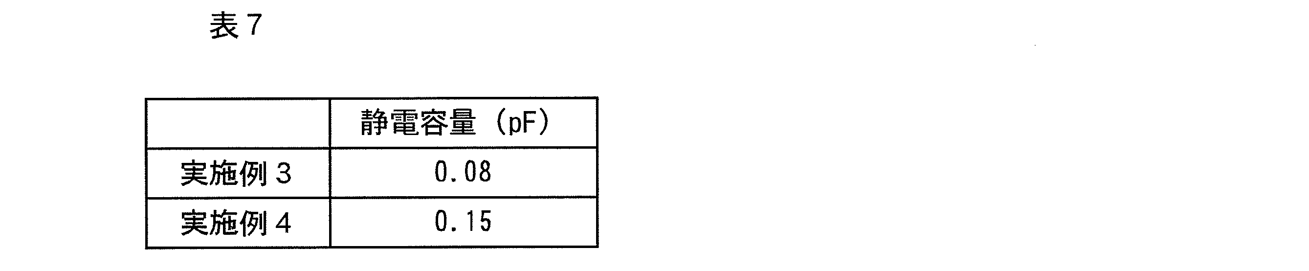
- Example 6 As is clear from Table 6, according to Examples 3 and 4, it can be seen that the discharge start voltage can be further reduced as compared with Example 2. That is, it can be seen that the discharge start voltage can be further reduced by forming the back electrode.
- Example 3 the electrostatic capacity is further increased as compared with Example 2. Thereby, it is considered that the charging action was further enhanced and the discharge start voltage could be further reduced.
- the capacitance was smaller than 0.5 pF, it was confirmed that it could be used for a high-frequency circuit.
Landscapes
- Elimination Of Static Electricity (AREA)
- Physics & Mathematics (AREA)
- Geometry (AREA)
- Engineering & Computer Science (AREA)
- Power Engineering (AREA)
- Thermistors And Varistors (AREA)
Abstract
Description
以下の要領で、第2の実施形態の実施例としての実施例1、2と、比較のための比較例1のESD保護装置を作製した。



平均粒径が2.5μmであり、Al含有量が7重量%のCuAl合金粉末と、平均粒径が0.5μmのBaO-Si2-Al2O3系ガラスセラミックス粉末と、ターピネオール中にエトセル樹脂を10重量%溶解した有機ビヒクル溶液を準備し、Cu合金粉末が全体の11.2体積%、上記BaO-Si2-Al2O3系ガラスセラミックス粉末が全体の2.8体積%、残りが上記有機ビヒクル溶液を占めるようにこれらを配合し、放電補助電極ペーストを得た。
平均粒径1μmの架橋アクリル樹脂ビーズ38重量%と、ターピネオール中にエトセル樹脂を10重量%溶解してなる有機ビヒクル溶液62重量%とを調合し、空洞形成ペーストを得た。
平均粒径が1μmのCu粉末80重量%と、ガラス転移点が620℃で、軟化点が720℃であり、平均粒径が1μmのホウケイ酸アルカリ系ガラスフリット5重量%と、エチルセルロースをターピネオールに溶解してなる有機ビヒクル15重量%とを混合し、外部端子電極用ペーストを得た。
平均粒径1μmのCu粉末を40重量%と、平均粒径3μmのCu粉末を40重量%と、エチルセルロースとターピネオールに溶解して作製した有機ビヒクルを20重量%とを調合し、3本ロールにより混合することにより、放電電極用ペーストを作製した。
上述したマザーのセラミックグリーンシート上に、上記高誘電率層ペーストを塗布し、次に上記補助電極ペーストを重ね塗りし、続いて第1,第2の放電電極を形成する位置に放電電極ペーストを重ね塗りした。ギャップの対向距離は20μmとした。さらに、上記空洞形成ペーストを塗布し、空洞上部には高誘電率層を重ね塗りし、乾燥した。
○…50%超~90%
△…10%超~50%
×…0%~10%


実施例2で用いた放電電極ペーストと同じ組成の電極ペーストを背後電極ペーストとして用意した。

2…基板
2a…上面
3,4…第1,第2の放電電極
5…放電補助電極
6…導電性を有しない材料で被覆されている導電性粒子
7,7A…高誘電率層
8,9…樹脂層
10,11…第1,第2の外部電極
12,12A…背後電極
21,31,41…ESD保護装置
22…基板
22b…空洞
Claims (15)
- 基板と、
前記基板に設けられており、ギャップを隔てて対向している第1,第2の放電電極と、
前記第1の放電電極と、前記第2の放電電極とを直接的又は間接的に接続するように設けられており、かつ前記基板より比誘電率が高い高誘電率層とを備える、ESD保護装置。 - 前記第1の放電電極と、前記第2の放電電極とを接続するように設けられており、前記第1,第2の放電電極間の放電を促す放電補助電極をさらに備える、請求項1に記載のESD保護装置。
- 前記放電補助電極が、導電性を有しない材料で被覆された導電性粒子を含む、請求項2に記載のESD保護装置。
- 前記高誘電率層が、前記放電補助電極に積層するように構成されている、請求項1~3のいずれか1項に記載のESD保護装置。
- 前記高誘電率層が、前記ギャップ部分の上方又は下方の少なくとも一方に設けられている、請求項1~4のいずれか1項に記載のESD保護装置。
- 前記ギャップに、前記基板よりも比誘電率が低い部分が位置している、請求項1~5のいずれか1項に記載のESD保護装置。
- 前記基板よりも比誘電率が低い部分が空洞である、請求項6に記載のESD保護装置。
- 前記基板よりも比誘電率が低い部分が、基板よりも比誘電率の低い材料からなる、請求項6に記載のESD保護装置。
- 前記基板よりも比誘電率が低い材料が樹脂である、請求項8に記載のESD保護装置。
- 前記第1,第2の放電電極間のギャップと前記基板の一部を介して重なり合うように設けられた背後電極をさらに備える、請求項1~9のいずれか1項に記載のESD保護装置。
- 前記基板に設けられており、前記第1,第2の放電電極にそれぞれ電気的に接続されている第1,第2の外部電極をさらに備え、
前記背後電極が、前記第1及び第2の外部電極のうちの一方に電気的に接続されている、請求項10に記載のESD保護装置。 - 前記背後電極が、浮き電極である、請求項10に記載のESD保護装置。
- 前記背後電極が、金属と、前記基板よりも高誘電率の材料とを含む、請求項10~12のいずれか1項に記載のESD保護装置。
- 前記第1,第2の放電電極が、前記基板の外表面に配置されている、請求項1~13のいずれか1項に記載のESD保護装置。
- 前記第1,第2の放電電極の先端が前記基板内に配置されており、前記ギャップが基板内に位置している、請求項1~13のいずれか1項に記載のESD保護装置。
Priority Applications (3)
| Application Number | Priority Date | Filing Date | Title |
|---|---|---|---|
| JP2015518141A JP6107945B2 (ja) | 2013-05-23 | 2014-04-01 | Esd保護装置 |
| CN201480029093.9A CN105229877B (zh) | 2013-05-23 | 2014-04-01 | Esd保护装置 |
| US14/930,833 US10193332B2 (en) | 2013-05-23 | 2015-11-03 | ESD protection device |
Applications Claiming Priority (2)
| Application Number | Priority Date | Filing Date | Title |
|---|---|---|---|
| JP2013109128 | 2013-05-23 | ||
| JP2013-109128 | 2013-05-23 |
Related Child Applications (1)
| Application Number | Title | Priority Date | Filing Date |
|---|---|---|---|
| US14/930,833 Continuation US10193332B2 (en) | 2013-05-23 | 2015-11-03 | ESD protection device |
Publications (1)
| Publication Number | Publication Date |
|---|---|
| WO2014188792A1 true WO2014188792A1 (ja) | 2014-11-27 |
Family
ID=51933358
Family Applications (1)
| Application Number | Title | Priority Date | Filing Date |
|---|---|---|---|
| PCT/JP2014/059616 Ceased WO2014188792A1 (ja) | 2013-05-23 | 2014-04-01 | Esd保護装置 |
Country Status (4)
| Country | Link |
|---|---|
| US (1) | US10193332B2 (ja) |
| JP (1) | JP6107945B2 (ja) |
| CN (1) | CN105229877B (ja) |
| WO (1) | WO2014188792A1 (ja) |
Cited By (1)
| Publication number | Priority date | Publication date | Assignee | Title |
|---|---|---|---|---|
| JP2024033858A (ja) * | 2022-08-31 | 2024-03-13 | Tdk株式会社 | 過渡電圧保護デバイス |
Families Citing this family (5)
| Publication number | Priority date | Publication date | Assignee | Title |
|---|---|---|---|---|
| JP6209966B2 (ja) * | 2013-12-26 | 2017-10-11 | Tdk株式会社 | 静電気保護部品 |
| US11178800B2 (en) * | 2018-11-19 | 2021-11-16 | Kemet Electronics Corporation | Ceramic overvoltage protection device having low capacitance and improved durability |
| TWI781418B (zh) * | 2019-07-19 | 2022-10-21 | 美商凱門特電子股份有限公司 | 具有低電容及改良耐用性的陶瓷過電壓保護裝置及其製造方法 |
| TWI790003B (zh) * | 2021-11-18 | 2023-01-11 | 佳邦科技股份有限公司 | 過電壓保護元件 |
| JP2024033860A (ja) * | 2022-08-31 | 2024-03-13 | Tdk株式会社 | 過渡電圧保護デバイス |
Citations (8)
| Publication number | Priority date | Publication date | Assignee | Title |
|---|---|---|---|---|
| JPH0883671A (ja) * | 1994-09-09 | 1996-03-26 | Mitsubishi Materials Corp | マイクロギャップ式サージアブソーバ |
| JPH11204232A (ja) * | 1998-01-13 | 1999-07-30 | Mitsubishi Materials Corp | 放電素子 |
| JP2002043021A (ja) * | 2000-07-31 | 2002-02-08 | Mitsubishi Materials Corp | チップ型サージアブソーバ |
| WO2009098944A1 (ja) * | 2008-02-05 | 2009-08-13 | Murata Manufacturing Co., Ltd. | Esd保護デバイス |
| JP2010146779A (ja) * | 2008-12-17 | 2010-07-01 | Panasonic Corp | 過電圧保護部品 |
| JP2010153719A (ja) * | 2008-12-26 | 2010-07-08 | Panasonic Corp | 過電圧保護部品およびその製造方法 |
| WO2011040435A1 (ja) * | 2009-09-30 | 2011-04-07 | 株式会社村田製作所 | Esd保護デバイスおよびその製造方法 |
| WO2012043534A1 (ja) * | 2010-09-29 | 2012-04-05 | 株式会社村田製作所 | Esd保護デバイスおよびその製造方法 |
Family Cites Families (4)
| Publication number | Priority date | Publication date | Assignee | Title |
|---|---|---|---|---|
| JP2001043954A (ja) | 1999-07-30 | 2001-02-16 | Tokin Corp | サージ吸収素子及びその製造方法 |
| JP2010015773A (ja) | 2008-07-02 | 2010-01-21 | Murata Mfg Co Ltd | サージアブソーバ及びその製造方法 |
| US8885324B2 (en) * | 2011-07-08 | 2014-11-11 | Kemet Electronics Corporation | Overvoltage protection component |
| US8658245B2 (en) * | 2011-08-31 | 2014-02-25 | Lexmark International, Inc. | Spin coat process for manufacturing a Z-directed component for a printed circuit board |
-
2014
- 2014-04-01 WO PCT/JP2014/059616 patent/WO2014188792A1/ja not_active Ceased
- 2014-04-01 CN CN201480029093.9A patent/CN105229877B/zh active Active
- 2014-04-01 JP JP2015518141A patent/JP6107945B2/ja active Active
-
2015
- 2015-11-03 US US14/930,833 patent/US10193332B2/en active Active
Patent Citations (8)
| Publication number | Priority date | Publication date | Assignee | Title |
|---|---|---|---|---|
| JPH0883671A (ja) * | 1994-09-09 | 1996-03-26 | Mitsubishi Materials Corp | マイクロギャップ式サージアブソーバ |
| JPH11204232A (ja) * | 1998-01-13 | 1999-07-30 | Mitsubishi Materials Corp | 放電素子 |
| JP2002043021A (ja) * | 2000-07-31 | 2002-02-08 | Mitsubishi Materials Corp | チップ型サージアブソーバ |
| WO2009098944A1 (ja) * | 2008-02-05 | 2009-08-13 | Murata Manufacturing Co., Ltd. | Esd保護デバイス |
| JP2010146779A (ja) * | 2008-12-17 | 2010-07-01 | Panasonic Corp | 過電圧保護部品 |
| JP2010153719A (ja) * | 2008-12-26 | 2010-07-08 | Panasonic Corp | 過電圧保護部品およびその製造方法 |
| WO2011040435A1 (ja) * | 2009-09-30 | 2011-04-07 | 株式会社村田製作所 | Esd保護デバイスおよびその製造方法 |
| WO2012043534A1 (ja) * | 2010-09-29 | 2012-04-05 | 株式会社村田製作所 | Esd保護デバイスおよびその製造方法 |
Cited By (1)
| Publication number | Priority date | Publication date | Assignee | Title |
|---|---|---|---|---|
| JP2024033858A (ja) * | 2022-08-31 | 2024-03-13 | Tdk株式会社 | 過渡電圧保護デバイス |
Also Published As
| Publication number | Publication date |
|---|---|
| CN105229877B (zh) | 2017-08-25 |
| US20160056627A1 (en) | 2016-02-25 |
| CN105229877A (zh) | 2016-01-06 |
| JPWO2014188792A1 (ja) | 2017-02-23 |
| US10193332B2 (en) | 2019-01-29 |
| JP6107945B2 (ja) | 2017-04-05 |
Similar Documents
| Publication | Publication Date | Title |
|---|---|---|
| CN101933204B (zh) | Esd保护器件 | |
| US8711537B2 (en) | ESD protection device and method for producing the same | |
| JP5590122B2 (ja) | Esd保護デバイス | |
| JP6107945B2 (ja) | Esd保護装置 | |
| JPWO2011040437A1 (ja) | Esd保護デバイスおよびその製造方法 | |
| WO2014199752A1 (ja) | セラミック電子部品およびその製造方法 | |
| JP2015043404A (ja) | 基板内蔵用積層セラミック電子部品及び積層セラミック電子部品内蔵型印刷回路基板 | |
| KR20120114337A (ko) | 정전기 대책 소자 | |
| WO2014141988A1 (ja) | 静電気対策素子 | |
| KR102076152B1 (ko) | 적층 세라믹 커패시터 및 적층 세라믹 커패시터 실장 기판 | |
| JP5561370B2 (ja) | Esd保護デバイスおよびその製造方法 | |
| CN112447396B (zh) | 多层电子组件 | |
| JP6075447B2 (ja) | Esd保護装置 | |
| JPWO2015190404A1 (ja) | 静電気放電保護デバイスおよびその製造方法 | |
| WO2014027552A1 (ja) | Esd保護装置 | |
| JP5757372B2 (ja) | Esd保護デバイス | |
| JP6079880B2 (ja) | Esd保護装置 | |
| CN205141366U (zh) | Esd保护装置 | |
| WO2013137032A1 (ja) | 静電気対策素子 | |
| US10057970B2 (en) | ESD protection device | |
| CN105340141B (zh) | Esd保护装置 | |
| CN207368416U (zh) | Esd保护装置 | |
| JP2017010850A (ja) | Esd保護装置 | |
| JP5644829B2 (ja) | Esd保護デバイスとその製造方法 | |
| JP2023028121A (ja) | 過渡電圧保護部品 |
Legal Events
| Date | Code | Title | Description |
|---|---|---|---|
| WWE | Wipo information: entry into national phase |
Ref document number: 201480029093.9 Country of ref document: CN |
|
| 121 | Ep: the epo has been informed by wipo that ep was designated in this application |
Ref document number: 14800411 Country of ref document: EP Kind code of ref document: A1 |
|
| ENP | Entry into the national phase |
Ref document number: 2015518141 Country of ref document: JP Kind code of ref document: A |
|
| NENP | Non-entry into the national phase |
Ref country code: DE |
|
| 122 | Ep: pct application non-entry in european phase |
Ref document number: 14800411 Country of ref document: EP Kind code of ref document: A1 |