WO2014171426A1 - タッチパネル用導電シートの製造方法、および、タッチパネル用導電シート - Google Patents
タッチパネル用導電シートの製造方法、および、タッチパネル用導電シート Download PDFInfo
- Publication number
- WO2014171426A1 WO2014171426A1 PCT/JP2014/060636 JP2014060636W WO2014171426A1 WO 2014171426 A1 WO2014171426 A1 WO 2014171426A1 JP 2014060636 W JP2014060636 W JP 2014060636W WO 2014171426 A1 WO2014171426 A1 WO 2014171426A1
- Authority
- WO
- WIPO (PCT)
- Prior art keywords
- wiring
- substrate
- detection electrode
- pad portion
- electrically connected
- Prior art date
Links
Images


Classifications
-
- G—PHYSICS
- G06—COMPUTING; CALCULATING OR COUNTING
- G06F—ELECTRIC DIGITAL DATA PROCESSING
- G06F3/00—Input arrangements for transferring data to be processed into a form capable of being handled by the computer; Output arrangements for transferring data from processing unit to output unit, e.g. interface arrangements
- G06F3/01—Input arrangements or combined input and output arrangements for interaction between user and computer
- G06F3/03—Arrangements for converting the position or the displacement of a member into a coded form
- G06F3/041—Digitisers, e.g. for touch screens or touch pads, characterised by the transducing means
- G06F3/044—Digitisers, e.g. for touch screens or touch pads, characterised by the transducing means by capacitive means
- G06F3/0445—Digitisers, e.g. for touch screens or touch pads, characterised by the transducing means by capacitive means using two or more layers of sensing electrodes, e.g. using two layers of electrodes separated by a dielectric layer
-
- G—PHYSICS
- G06—COMPUTING; CALCULATING OR COUNTING
- G06F—ELECTRIC DIGITAL DATA PROCESSING
- G06F3/00—Input arrangements for transferring data to be processed into a form capable of being handled by the computer; Output arrangements for transferring data from processing unit to output unit, e.g. interface arrangements
- G06F3/01—Input arrangements or combined input and output arrangements for interaction between user and computer
- G06F3/03—Arrangements for converting the position or the displacement of a member into a coded form
- G06F3/041—Digitisers, e.g. for touch screens or touch pads, characterised by the transducing means
- G06F3/0416—Control or interface arrangements specially adapted for digitisers
- G06F3/04164—Connections between sensors and controllers, e.g. routing lines between electrodes and connection pads
-
- G—PHYSICS
- G06—COMPUTING; CALCULATING OR COUNTING
- G06F—ELECTRIC DIGITAL DATA PROCESSING
- G06F3/00—Input arrangements for transferring data to be processed into a form capable of being handled by the computer; Output arrangements for transferring data from processing unit to output unit, e.g. interface arrangements
- G06F3/01—Input arrangements or combined input and output arrangements for interaction between user and computer
- G06F3/03—Arrangements for converting the position or the displacement of a member into a coded form
- G06F3/041—Digitisers, e.g. for touch screens or touch pads, characterised by the transducing means
- G06F3/044—Digitisers, e.g. for touch screens or touch pads, characterised by the transducing means by capacitive means
- G06F3/0446—Digitisers, e.g. for touch screens or touch pads, characterised by the transducing means by capacitive means using a grid-like structure of electrodes in at least two directions, e.g. using row and column electrodes
-
- G—PHYSICS
- G06—COMPUTING; CALCULATING OR COUNTING
- G06F—ELECTRIC DIGITAL DATA PROCESSING
- G06F3/00—Input arrangements for transferring data to be processed into a form capable of being handled by the computer; Output arrangements for transferring data from processing unit to output unit, e.g. interface arrangements
- G06F3/01—Input arrangements or combined input and output arrangements for interaction between user and computer
- G06F3/03—Arrangements for converting the position or the displacement of a member into a coded form
- G06F3/041—Digitisers, e.g. for touch screens or touch pads, characterised by the transducing means
- G06F3/047—Digitisers, e.g. for touch screens or touch pads, characterised by the transducing means using sets of wires, e.g. crossed wires
-
- H—ELECTRICITY
- H05—ELECTRIC TECHNIQUES NOT OTHERWISE PROVIDED FOR
- H05K—PRINTED CIRCUITS; CASINGS OR CONSTRUCTIONAL DETAILS OF ELECTRIC APPARATUS; MANUFACTURE OF ASSEMBLAGES OF ELECTRICAL COMPONENTS
- H05K1/00—Printed circuits
- H05K1/02—Details
- H05K1/0296—Conductive pattern lay-out details not covered by sub groups H05K1/02 - H05K1/0295
-
- H—ELECTRICITY
- H05—ELECTRIC TECHNIQUES NOT OTHERWISE PROVIDED FOR
- H05K—PRINTED CIRCUITS; CASINGS OR CONSTRUCTIONAL DETAILS OF ELECTRIC APPARATUS; MANUFACTURE OF ASSEMBLAGES OF ELECTRICAL COMPONENTS
- H05K1/00—Printed circuits
- H05K1/02—Details
- H05K1/11—Printed elements for providing electric connections to or between printed circuits
- H05K1/115—Via connections; Lands around holes or via connections
-
- H—ELECTRICITY
- H05—ELECTRIC TECHNIQUES NOT OTHERWISE PROVIDED FOR
- H05K—PRINTED CIRCUITS; CASINGS OR CONSTRUCTIONAL DETAILS OF ELECTRIC APPARATUS; MANUFACTURE OF ASSEMBLAGES OF ELECTRICAL COMPONENTS
- H05K3/00—Apparatus or processes for manufacturing printed circuits
- H05K3/40—Forming printed elements for providing electric connections to or between printed circuits
- H05K3/4007—Surface contacts, e.g. bumps
-
- H—ELECTRICITY
- H05—ELECTRIC TECHNIQUES NOT OTHERWISE PROVIDED FOR
- H05K—PRINTED CIRCUITS; CASINGS OR CONSTRUCTIONAL DETAILS OF ELECTRIC APPARATUS; MANUFACTURE OF ASSEMBLAGES OF ELECTRICAL COMPONENTS
- H05K3/00—Apparatus or processes for manufacturing printed circuits
- H05K3/40—Forming printed elements for providing electric connections to or between printed circuits
- H05K3/4038—Through-connections; Vertical interconnect access [VIA] connections
-
- G—PHYSICS
- G06—COMPUTING; CALCULATING OR COUNTING
- G06F—ELECTRIC DIGITAL DATA PROCESSING
- G06F2203/00—Indexing scheme relating to G06F3/00 - G06F3/048
- G06F2203/041—Indexing scheme relating to G06F3/041 - G06F3/045
- G06F2203/04103—Manufacturing, i.e. details related to manufacturing processes specially suited for touch sensitive devices
-
- G—PHYSICS
- G06—COMPUTING; CALCULATING OR COUNTING
- G06F—ELECTRIC DIGITAL DATA PROCESSING
- G06F2203/00—Indexing scheme relating to G06F3/00 - G06F3/048
- G06F2203/041—Indexing scheme relating to G06F3/041 - G06F3/045
- G06F2203/04112—Electrode mesh in capacitive digitiser: electrode for touch sensing is formed of a mesh of very fine, normally metallic, interconnected lines that are almost invisible to see. This provides a quite large but transparent electrode surface, without need for ITO or similar transparent conductive material
-
- H—ELECTRICITY
- H05—ELECTRIC TECHNIQUES NOT OTHERWISE PROVIDED FOR
- H05K—PRINTED CIRCUITS; CASINGS OR CONSTRUCTIONAL DETAILS OF ELECTRIC APPARATUS; MANUFACTURE OF ASSEMBLAGES OF ELECTRICAL COMPONENTS
- H05K2201/00—Indexing scheme relating to printed circuits covered by H05K1/00
- H05K2201/09—Shape and layout
- H05K2201/09209—Shape and layout details of conductors
- H05K2201/095—Conductive through-holes or vias
- H05K2201/09563—Metal filled via
-
- H—ELECTRICITY
- H05—ELECTRIC TECHNIQUES NOT OTHERWISE PROVIDED FOR
- H05K—PRINTED CIRCUITS; CASINGS OR CONSTRUCTIONAL DETAILS OF ELECTRIC APPARATUS; MANUFACTURE OF ASSEMBLAGES OF ELECTRICAL COMPONENTS
- H05K2201/00—Indexing scheme relating to printed circuits covered by H05K1/00
- H05K2201/09—Shape and layout
- H05K2201/09209—Shape and layout details of conductors
- H05K2201/09654—Shape and layout details of conductors covering at least two types of conductors provided for in H05K2201/09218 - H05K2201/095
- H05K2201/09681—Mesh conductors, e.g. as a ground plane
-
- H—ELECTRICITY
- H05—ELECTRIC TECHNIQUES NOT OTHERWISE PROVIDED FOR
- H05K—PRINTED CIRCUITS; CASINGS OR CONSTRUCTIONAL DETAILS OF ELECTRIC APPARATUS; MANUFACTURE OF ASSEMBLAGES OF ELECTRICAL COMPONENTS
- H05K2203/00—Indexing scheme relating to apparatus or processes for manufacturing printed circuits covered by H05K3/00
- H05K2203/12—Using specific substances
- H05K2203/125—Inorganic compounds, e.g. silver salt
-
- H—ELECTRICITY
- H05—ELECTRIC TECHNIQUES NOT OTHERWISE PROVIDED FOR
- H05K—PRINTED CIRCUITS; CASINGS OR CONSTRUCTIONAL DETAILS OF ELECTRIC APPARATUS; MANUFACTURE OF ASSEMBLAGES OF ELECTRICAL COMPONENTS
- H05K3/00—Apparatus or processes for manufacturing printed circuits
- H05K3/10—Apparatus or processes for manufacturing printed circuits in which conductive material is applied to the insulating support in such a manner as to form the desired conductive pattern
- H05K3/105—Apparatus or processes for manufacturing printed circuits in which conductive material is applied to the insulating support in such a manner as to form the desired conductive pattern by conversion of non-conductive material on or in the support into conductive material, e.g. by using an energy beam
- H05K3/106—Apparatus or processes for manufacturing printed circuits in which conductive material is applied to the insulating support in such a manner as to form the desired conductive pattern by conversion of non-conductive material on or in the support into conductive material, e.g. by using an energy beam by photographic methods
-
- H—ELECTRICITY
- H05—ELECTRIC TECHNIQUES NOT OTHERWISE PROVIDED FOR
- H05K—PRINTED CIRCUITS; CASINGS OR CONSTRUCTIONAL DETAILS OF ELECTRIC APPARATUS; MANUFACTURE OF ASSEMBLAGES OF ELECTRICAL COMPONENTS
- H05K3/00—Apparatus or processes for manufacturing printed circuits
- H05K3/40—Forming printed elements for providing electric connections to or between printed circuits
- H05K3/4038—Through-connections; Vertical interconnect access [VIA] connections
- H05K3/4053—Through-connections; Vertical interconnect access [VIA] connections by thick-film techniques
Definitions
- the present invention relates to a method for producing a conductive sheet for a touch panel and a conductive sheet for a touch panel.
- Conductive sheets with conductive thin wires formed on substrates are widely used in transparent electrodes for various electronic devices such as solar cells, inorganic EL elements, and organic EL elements, electromagnetic wave shields for various display devices, touch panels, and transparent sheet heating elements. It's being used. In particular, in recent years, the rate of mounting touch panels on mobile phones, portable game devices, and the like has increased, and the demand for conductive sheets for capacitive touch panels capable of multipoint detection is rapidly expanding.
- a substrate As one aspect of the conductive sheet for the touch panel, a substrate, a detection electrode for detecting an input position provided on the front surface and the back surface of the substrate, and a lead-out wiring for applying a voltage to the detection electrode are provided.
- a flexible printed wiring board is connected to one end of the lead wiring.
- the lead-out wiring exists on the front surface and the back surface of the substrate, it is necessary to bond the flexible printed wiring board to both surfaces.
- there are many bonded portions there is a concern that moisture easily enters and durability is inferior. .
- Patent Document 1 discloses a mode in which the end portion of the lead-out wiring is drawn out to the surface side through a conductive material filled in the through hole.
- the detection electrodes (corresponding to the first and second electrode patterns in Patent Document 1) are formed of a transparent conductive material mainly composed of an organic conductive polymer, and lead wires (in Patent Document 1).
- the wiring patterns 16 and 17) are disclosed to be formed by screen printing using silver paste or the like. That is, it describes that after the detection electrode is manufactured, the lead-out wiring connected to the detection electrode is formed by screen printing or the like in a separate process. In the case of such a method, when applying the silver paste after producing the detection electrode, it is necessary to perform alignment (alignment adjustment) again to determine the application position. There is concern about the decline.
- an object of the present invention is to provide a method for manufacturing a conductive sheet for a touch panel in which ends of lead-out wirings are gathered on one side of a substrate more easily and with high productivity.
- a method for producing a conductive sheet for a touch panel A first detection electrode on the back surface of the substrate, a back surface side wiring having one end electrically connected to the first detection electrode and a first pad portion on the other end, and a second on the surface of the substrate Forming a detection electrode, a second lead wire electrically connected to the second detection electrode, and a second pad portion disposed at a position facing the first pad portion via the substrate; Forming a through-hole penetrating the first pad portion, the substrate, and the second pad portion; A through wiring is formed by filling the through hole with a conductive material to electrically connect the first pad portion and the second pad portion, and includes a back surface side wiring and a through wiring, and is electrically connected to the first detection electrode.
- a method of manufacturing a conductive sheet for a touch panel (2) A method for manufacturing a conductive sheet for a touch panel, A first detection electrode and a first pad portion electrically connected to an end of the first detection electrode are formed on the back surface of the substrate, and a second detection electrode and a second detection electrode are formed on the surface of the substrate. A second lead wire electrically connected to the first pad portion, a second pad portion disposed at a position facing the first pad portion via the substrate, and a wiring portion electrically connected to the second pad portion.
- Forming a surface-side wiring having: Forming a through-hole penetrating the first pad portion, the substrate, and the second pad portion; The through hole is filled with a conductive material to produce a through wiring that electrically connects the first pad portion and the second pad portion, and includes the surface side wiring and the through wiring, and is electrically connected to the first detection electrode.
- a method for manufacturing a conductive sheet for a touch panel A first detection electrode on the back surface of the substrate, a back surface side wiring having one end electrically connected to the first detection electrode and a first pad portion on the other end, and a second on the surface of the substrate
- the detection electrode, the second lead wire electrically connected to the second detection electrode, and the second pad portion and the second pad portion arranged at positions facing the first pad portion via the substrate are electrically connected
- a through-wiring is formed by filling the through-hole with a conductive material to electrically connect the first pad portion and the second pad portion, and includes a front-side wiring, a through-wiring, and a back-side wiring.
- a substrate A first detection electrode disposed on the back surface of the substrate; A first lead wire, one end of which is electrically connected to the first detection electrode, the other end is disposed on the surface of the substrate, and includes a part of a through wire penetrating the substrate; A second sensing electrode disposed on the surface of the substrate; A second lead line electrically connected to the second detection electrode; A conductive sheet for a touch panel, wherein the first detection electrode, the second detection electrode, the first lead wiring, and the second lead wiring include the same metal material.
- the present invention it is possible to provide a method for producing a conductive sheet for a touch panel in which the ends of the lead-out wiring are collected on one side of the substrate more easily and with high productivity.
- FIG. 2 is a cross-sectional view taken along a cutting line AA shown in FIG.
- FIG. 2 is a cross-sectional view taken along a cutting line BB shown in FIG.
- It is a partial expanded sectional view which shows the through-hole formed at process B1 of the 1st embodiment of the manufacturing method of the electrically conductive sheet for touchscreens of this invention.
- FIG. 8 is a cross-sectional view taken along a cutting line CC shown in FIG. It is a top view of the board
- FIG. 10 is a cross-sectional view taken along a cutting line DD shown in FIG. 9.
- a detection electrode and a portion that becomes a part of the lead wiring are formed on the surface of the substrate. Forming and then providing a through-wiring that penetrates the substrate and drawing the lead-out wiring from the back surface side to the front surface side can be mentioned.
- a part that becomes a part of the detection electrode and the lead-out wiring is first manufactured on the substrate, and then a through-wiring is manufactured. There is no need to perform alignment, and a desired conductive sheet can be manufactured more easily.
- the first embodiment of the method for manufacturing a conductive sheet for a touch panel (hereinafter also simply referred to as a conductive sheet) according to the present invention includes a step A1 for forming a detection electrode and a lead-out wiring on a substrate and a through hole at a predetermined position. And a process C1 for filling the through hole with a conductive material.
- Step A1 includes forming a first detection electrode on the back surface of the substrate, and a back surface side wiring having one end electrically connected to the first detection electrode and having the first pad portion on the other end, and the surface of the substrate Forming a second detection electrode, a second lead wire electrically connected to the second detection electrode, and a second pad portion disposed at a position facing the first pad portion via the substrate; is there.
- FIG. 1 the top view of the board
- FIG. 2 is a cross-sectional view taken along the cutting line AA.
- FIG. 3 is a cross-sectional view taken along the cutting line BB.
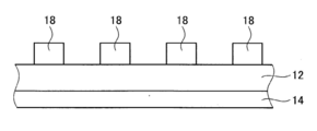
- the substrate with wiring 10 obtained by the step A ⁇ b> 1 includes the substrate 12, the first detection electrode 14 disposed on the back surface of the substrate 12, the back surface side wiring 16, and the substrate 12.
- a second detection electrode 18, a second lead-out wiring 20, and a second pad portion 36 are provided on the surface.
- an input area E I that can be input by a user and an outer area E located outside the input area E I. O.
- first detection electrode 14 and the second detection electrode 18 are arranged in the input region E I , and a first extraction wiring and a second extraction wiring to be described later are arranged in the outer region E O.
- first detection electrode 14 and the second detection electrode 18 are arranged in the input region E I , and a first extraction wiring and a second extraction wiring to be described later are arranged in the outer region E O.
- the substrate 12 is a member that plays a role of supporting the first detection electrode 14 and the second detection electrode 18 in the input region E I and a role of supporting the first lead wiring and the second lead wiring in the outer region E O. is there. It is preferable that the substrate 12 appropriately transmits light. Specifically, the total light transmittance of the substrate 12 is preferably 85 to 100%.
- the substrate 12 preferably has an insulating property. That is, the substrate 12 is a substrate (insulating substrate) for ensuring insulation between the first detection electrode 14 and the second detection electrode 18.
- the substrate 12 is preferably a transparent substrate.
- an insulating resin substrate is preferable because of its excellent toughness.
- the material constituting the insulating resin substrate is a polyethylene terephthalate resin, a polyethersulfone resin, a polyacrylic resin, a polyurethane resin, a polyester resin, a polycarbonate resin, a polysulfone resin, or a polyamide resin.
- polyethylene terephthalate resins, cycloolefin resins, polycarbonate resins, and triacetyl cellulose resins are preferable because of excellent transparency.
- the substrate 12 is a single layer, but may be a multilayer of two or more layers.
- the thickness of the substrate 12 (when the substrate 12 is a multilayer of two or more layers, the total thickness thereof) is not particularly limited, but is preferably 5 to 350 ⁇ m, and more preferably 30 to 150 ⁇ m. Within the above range, desired visible light transmittance can be obtained, and handling is easy.
- the planar view shape of the substrate 12 is substantially rectangular, but is not limited thereto. For example, it may be circular or polygonal.
- the 1st detection electrode 14 and the 2nd detection electrode 18 comprise the part (sensing part) which functions as a sensing electrode which senses the change of an electrostatic capacitance in the touch panel containing the conductive sheet of this invention. That is, when the fingertip is brought into contact with the touch panel, the mutual capacitance between the first detection electrode 14 and the second detection electrode 18 changes, and the position of the fingertip is calculated by the IC circuit based on the change amount.
- the first detection electrodes 14 are electrodes that extend in the first direction (Y direction) and are arranged at predetermined intervals in a second direction (X direction) orthogonal to the first direction. Includes patterns.
- the second detection electrodes 18 extend in the second direction (X direction) and are arranged at a predetermined interval in the first direction (Y direction), and include a predetermined pattern as will be described later.
- five first detection electrodes 14 and five second detection electrodes 18 are provided, but the number is not particularly limited and may be plural.
- the first detection electrode 14 and the second detection electrode 18 are composed of conductive thin wires.
- FIG. 4 shows an enlarged plan view of a part of the first detection electrode 14.
- the first detection electrode 14 is composed of conductive thin wires 22 and includes a plurality of grids 24 formed by intersecting conductive thin wires 22.
- the second detection electrode 18 also includes a plurality of grids 24 formed by intersecting conductive thin wires 22.
- Examples of the conductive material included in the conductive thin wire 22 include metals and alloys such as gold (Au), silver (Ag), copper (Cu), and aluminum (Al), ITO, tin oxide, zinc oxide, cadmium oxide, Examples thereof include metal oxides such as gallium oxide and titanium oxide. Among these, silver is preferable because the conductivity of the conductive thin wire 22 is excellent.
- the conductive fine wire 22 preferably contains a binder.
- the binder is preferably a water-soluble polymer because the adhesiveness between the conductive thin wire 22 and the substrate 12 is more excellent.
- binders include gelatin, carrageenan, polyvinyl alcohol (PVA), polyvinyl pyrrolidone (PVP), starch and other polysaccharides, cellulose and its derivatives, polyethylene oxide, polysaccharides, polyvinylamine, chitosan, polylysine, and polyacryl. Examples include acid, polyalginic acid, polyhyaluronic acid, carboxycellulose, gum arabic, and sodium alginate.
- gelatin is preferable because the adhesion between the conductive fine wire 22 and the substrate 12 is more excellent.
- acid-processed gelatin may be used as gelatin, and gelatin hydrolyzate, gelatin enzyme decomposition product, and other gelatins modified with amino groups and carboxyl groups (phthalated gelatin, acetylated gelatin) Can be used.
- the volume ratio of metal to binder is preferably 1.0 or more, and more preferably 1.5 or more.
- the upper limit is not particularly limited, but is preferably 4.0 or less and more preferably 2.5 or less from the viewpoint of productivity.
- the volume ratio between the metal and the binder can be calculated from the density of the metal and the binder contained in the conductive thin wire 22. For example, when the metal is silver, the density of silver is 10.5 g / cm 3 , and when the binder is gelatin, the density of gelatin is 1.34 g / cm 3 .
- One preferred embodiment of the conductive thin wire 22 includes an embodiment in which metallic silver, gelatin, and a polymer different from gelatin are included.
- a polymer different from gelatin (hereinafter also simply referred to as a polymer) is preferably a polymer containing no protein. More specifically, for example, acrylic resins, styrene resins, vinyl resins, polyolefin resins, polyester resins, polyurethane resins, polyamide resins, polycarbonate resins, polydiene resins, epoxy resins, silicone resins. Examples thereof include at least one resin selected from the group consisting of a resin, a cellulose-based resin, and a chitosan-based resin, or a copolymer composed of monomers constituting these resins.
- a polymer that is not degraded by a proteolytic enzyme is preferable, and examples thereof include acrylic resins, styrene resins, and polyester resins.
- the polymer may contain a group (reactive group) capable of reacting with a crosslinkable group in a crosslinking agent described later.
- the polymer (copolymer) represented by the following general formula (1) is mentioned as a suitable aspect of the said polymer from the point which can prevent more permeation
- A, B, C, and D each represent the following repeating unit.
- R 1 represents a methyl group or a halogen atom, preferably a methyl group, a chlorine atom, or a bromine atom.
- p represents an integer of 0 to 2, preferably 0 or 1, and more preferably 0.
- R 2 represents a methyl group or an ethyl group, and a methyl group is preferable.
- R 3 represents a hydrogen atom or a methyl group, preferably a hydrogen atom.
- L represents a divalent linking group, preferably a group represented by the following general formula (2).
- Formula (2) — (CO—X 1 ) r—X 2 —
- X 1 represents an oxygen atom or —NR 30 —.
- R 30 represents a hydrogen atom, an alkyl group, an aryl group, or an acyl group, and each may have a substituent (for example, a halogen atom, a nitro group, a hydroxyl group, etc.).
- R 30 is preferably a hydrogen atom, an alkyl group having 1 to 10 carbon atoms (for example, methyl group, ethyl group, n-butyl group, n-octyl group, etc.), acyl group (for example, acetyl group, benzoyl group, etc.) It is. Particularly preferred as X 1 is an oxygen atom or —NH—.
- X 2 represents an alkylene group, an arylene group, an alkylene arylene group, an arylene alkylene group, or an alkylene arylene alkylene group, and these groups include —O—, —S—, —OCO—, —CO—, —COO—.
- R 31 represents a linear or branched alkyl group having 1 to 6 carbon atoms, such as a methyl group, an ethyl group, and an isopropyl group.
- Preferred examples of X 2 include dimethylene group, trimethylene group, tetramethylene group, o-phenylene group, m-phenylene group, p-phenylene group, —CH 2 CH 2 OCOCH 2 CH 2 —, —CH 2 CH 2 OCO ( C 6 H 4 ) — and the like.
- r represents 0 or 1; q represents 0 or 1, and 0 is preferable.
- R 4 represents an alkyl group having 5 to 80 carbon atoms, an alkenyl group, or an alkynyl group, preferably an alkyl group having 5 to 50 carbon atoms, more preferably an alkyl group having 5 to 30 carbon atoms, More preferred is an alkyl group having 5 to 20 carbon atoms.
- R 5 is a hydrogen atom, a methyl group, an ethyl group, a halogen atom, or a -CH 2 COOR 6, a hydrogen atom, a methyl group, a halogen atom, -CH 2 COOR 6 are preferred, hydrogen atom, a methyl group, -CH 2 COOR 6 is more preferable, and a hydrogen atom is particularly preferable.
- R 6 represents a hydrogen atom or an alkyl group having 1 to 80 carbon atoms, and may be the same as or different from R 4.
- the number of carbon atoms in R 6 is preferably 1 to 70, more preferably 1 to 60.
- x, y, z, and w represent the molar ratio of each repeating unit.
- x is 3 to 60 mol%, preferably 3 to 50 mol%, more preferably 3 to 40 mol%.
- y is 30 to 96 mol%, preferably 35 to 95 mol%, particularly preferably 40 to 90 mol%. If z is too small, the affinity with a hydrophilic protective colloid such as gelatin decreases, so the probability of occurrence of agglomeration / peeling failure of the matting agent increases. The matting agent of the present invention is dissolved. Therefore, z is 0.5 to 25 mol%, preferably 0.5 to 20 mol%, particularly preferably 1 to 20 mol%.
- w is 0.5 to 40 mol%, preferably 0.5 to 30 mol%.
- x is 3 to 40 mol%
- y is 40 to 90 mol%
- z is 0.5 to 20 mol%
- w is 0.5 to 10 mol%.
- the polymer represented by the general formula (1) is preferably a polymer represented by the following general formula (2).
- the polymer represented by the general formula (1) may include other repeating units other than the general formulas (A), (B), (C) and (D).
- Examples of monomers for forming other repeating units include acrylic acid esters, methacrylic acid esters, vinyl esters, olefins, crotonic acid esters, itaconic acid diesters, maleic acid diesters, and fumaric acid diesters. , Acrylamides, unsaturated carboxylic acids, allyl compounds, vinyl ethers, vinyl ketones, vinyl heterocycles, glycidyl esters, unsaturated nitriles, and the like. These monomers are also described in [0010] to [0022] of Japanese Patent No. 3754745.
- the polymer represented by the general formula (1) preferably contains a repeating unit represented by the following general formula (E) in addition to the above general formulas (A), (B), (C) and (D).
- L E represents an alkylene group, preferably an alkylene group having 1 to 10 carbon atoms, more preferably an alkylene group having 2 to 6 carbon atoms, and still more preferably an alkylene group having 2 to 4 carbon atoms.
- a polymer represented by the following general formula (3) is particularly preferable.
- a1, b1, c1, d1, and e1 represent the molar ratio of each monomer unit, a1 is 3 to 60 (mol%), b1 is 30 to 95 (mol%), and c1 is 0.5 to 25 (mol%), d1 represents 0.5 to 40 (mol%), and e1 represents 1 to 10 (mol%).
- the preferred range of a1 is the same as the preferred range of x
- the preferred range of b1 is the same as the preferred range of y
- the preferred range of c1 is the same as the preferred range of z
- the preferred range of d1 is The same as the preferable range of w.
- e1 is 1 to 10 mol%, preferably 2 to 9 mol%, more preferably 2 to 8 mol%.
- the weight average molecular weight of the polymer represented by the general formula (1) is preferably 1,000 to 1,000,000, more preferably 2000 to 750,000, and still more preferably 3000 to 500,000.
- the polymer represented by the general formula (1) can be synthesized with reference to, for example, Japanese Patent No. 3305459 and Japanese Patent No. 3754745.
- the line width of the conductive thin wire 22 is not particularly limited, but is preferably 30 ⁇ m or less, more preferably 15 ⁇ m or less, still more preferably 10 ⁇ m or less, and particularly preferably 9 ⁇ m or less, from the viewpoint that a low-resistance electrode can be formed relatively easily. 7 ⁇ m or less is most preferable, 0.5 ⁇ m or more is preferable, and 1.0 ⁇ m or more is more preferable.
- the thickness of the conductive thin wire 22 is not particularly limited, but can be selected from 0.00001 mm to 0.2 mm from the viewpoint of conductivity and visibility, but is preferably 30 ⁇ m or less, more preferably 20 ⁇ m or less, Is more preferably from 9 to 9 ⁇ m, most preferably from 0.05 to 5 ⁇ m.
- the lattice 24 includes an opening region surrounded by the thin conductive wires 22.
- the length W of one side of the grating 24 is preferably 800 ⁇ m or less, more preferably 600 ⁇ m or less, and preferably 50 ⁇ m or more.
- the aperture ratio is preferably 85% or more, more preferably 90% or more, and most preferably 95% or more in terms of visible light transmittance. preferable.
- the aperture ratio corresponds to the ratio of the transmissive portion excluding the conductive thin wires 22 in the first detection electrode 14 or the second detection electrode 18 in the predetermined region.
- the lattice 24 has a substantially rhombus shape.
- other polygonal shapes for example, a triangle, a quadrangle, a hexagon, and a random polygon
- the shape of one side may be a curved shape or a circular arc shape in addition to a linear shape.
- the arc shape for example, the two opposing sides may have an outwardly convex arc shape, and the other two opposing sides may have an inwardly convex arc shape.
- the shape of each side may be a wavy shape in which an outwardly convex arc and an inwardly convex arc are continuous. Of course, the shape of each side may be a sine curve.
- the conductive thin wire 22 is formed as a mesh pattern, but is not limited to this mode, and may be a stripe pattern.
- the first detection electrode 14 and the second detection electrode 18 have a mesh structure of conductive thin wires 22, but are not limited to this mode.
- a metal oxide such as ITO or ZnO is used.
- You may be comprised with metal nanowire particles, such as a metal thin film, metal oxide particles, metal pastes, such as silver paste and copper paste, silver nanowire, and copper nanowire.
- silver nanowires are preferable because they are excellent in conductivity and transparency.
- the patterning of the first detection electrode 14 and the second detection electrode 18 can be selected according to the material of the electrode part, and a photolithography method, a resist mask screen printing-etching method, an inkjet method, a printing method, or the like may be used. .
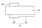
- the back surface side wiring 16 has a wiring part 32 and a first pad part 34, one end of which is electrically connected to the end part of the first detection electrode 14, and the other end is a first pad.
- the wiring has a portion 34. Note that one end of the wiring portion 32 is electrically connected to the first detection electrode 14, and the other end is electrically connected to the first pad portion 34.
- the back surface side wiring 16 is electrically connected to the first detection electrode 14 through a process described later, and forms a first lead wiring whose one end is located on the front surface side of the substrate 12. That is, the back surface side wiring 16 is a part of the first lead wiring.
- the back surface side wiring 16 is disposed on the substrate 12 in the outer region EO . In FIG.
- the number is not particularly limited, and a plurality of wirings are usually arranged according to the number of detection electrodes.
- the heights of the wiring part 32 and the first pad part 34 are different, but they may be the same height.
- the material that constitutes the back surface side wiring 16 is not particularly limited.
- a metal or alloy such as gold (Au), silver (Ag), copper (Cu), or aluminum (Al), ITO, tin oxide, zinc oxide, oxidation Examples thereof include metal oxides such as cadmium, gallium oxide, and titanium oxide.
- silver is preferable because of its excellent conductivity.
- the back surface side wiring 16 preferably contains a binder.
- the kind of the binder is as described above (for example, gelatin, a polymer different from gelatin, etc.).
- the first pad portion 34 is electrically connected to a second pad portion 36 described later via a through wiring.
- the second pad portion 36 is located in the external conductive region G where the flexible printed wiring board and the like are disposed, and the first pad portion 34 is also connected to the external conductive region G on the surface of the substrate 12 and the substrate. It arrange
- the first pad portion 34 has a circular shape, but the shape is not particularly limited.
- the diameter of the first pad portion 34 is larger than the width of the wiring portion 32, but the size is not particularly limited.
- the second lead wiring 20 is a member that plays a role in applying a voltage to the second detection electrode 18.
- the second lead wiring 20 is disposed on the substrate 12 in the outer region E O , one end of which is electrically connected to the corresponding end of the second detection electrode 18, and the other end is disposed with a flexible printed wiring board or the like. And a pad portion (external connection pad portion) (not shown).
- five second lead wires 20 are described, but the number is not particularly limited, and a plurality of second lead wires 20 are usually arranged according to the number of detection electrodes.
- the material which comprises the 2nd extraction wiring 20 in particular is not restrict
- the 2nd pad part 36 is arrange
- the second pad portion 36 is disposed at a position facing the first pad portion 34 with the substrate 12 interposed therebetween. That is, as shown in FIG. 1, when the board
- the material constituting the second pad portion 36 is not particularly limited.
- the second pad portion 36 preferably contains a binder.
- the kind of binder is as above-mentioned.
- the second pad portion 36 has a circular shape, but the shape is not particularly limited.
- the size of the second pad portion 36 is not particularly limited, but is preferably the same size as the first pad portion 34 in terms of producing a through-hole described later. In FIG. 1, five second pad portions 36 are described, but the number is not particularly limited, and a plurality of second pad portions 36 are usually arranged according to the number of detection electrodes.
- the first detection electrode 14 and the back surface side wiring 16 on the front surface and the back surface of the substrate 12, and the portions other than the second detection electrode 18, the second lead wiring 20, and the second pad portion 36 have a binder portion. Further, it may be arranged.
- the binder part includes gelatin and a polymer different from gelatin.
- ⁇ Method for Forming Substrate with Wiring 10> The formation method of the board
- a silver halide emulsion layer hereinafter also referred to simply as a photosensitive layer
- Step (1) is a step of forming a photosensitive layer containing silver halide and gelatin on both surfaces of the substrate 12.
- the method for forming the photosensitive layer is not particularly limited, but from the viewpoint of productivity, the photosensitive layer forming composition containing silver halide and gelatin is brought into contact with the substrate 12, and the photosensitive layer is formed on both surfaces of the substrate 12.
- the method of forming is preferred. Below, after explaining in full detail the aspect of the composition for photosensitive layer formation used with the said method, the procedure of a process is explained in full detail.
- the composition for forming a photosensitive layer contains silver halide and gelatin.
- the halogen element contained in the silver halide may be any of chlorine, bromine, iodine and fluorine, or a combination thereof.
- As the silver halide for example, a silver halide mainly composed of silver chloride, silver bromide or silver iodide is preferably used, and further a silver halide mainly composed of silver bromide or silver chloride is preferably used.
- the types of gelatin are as described above.
- the volume ratio of silver halide and gelatin contained in the composition for forming a photosensitive layer is not particularly limited, and is appropriately adjusted so as to be within a preferable volume ratio range of the metal and the binder in the conductive thin wire 22 described above. Is done.
- the composition for forming a photosensitive layer contains a solvent, if necessary.
- the solvent used include water, organic solvents (for example, alcohols such as methanol, ketones such as acetone, amides such as formamide, sulfoxides such as dimethyl sulfoxide, esters such as ethyl acetate, ethers, and the like. Etc.), ionic liquids, or mixed solvents thereof.
- the content of the solvent to be used is not particularly limited, but is preferably in the range of 30 to 90% by mass, and more preferably in the range of 50 to 80% by mass with respect to the total mass of silver halide and binder.
- composition for photosensitive layer formation other materials other than the material mentioned above may be contained as needed.
- materials include metal compounds belonging to Group VIII and VIIB such as rhodium compounds and iridium compounds used for stabilizing silver halide and increasing sensitivity.
- an antistatic agent e.g., a nucleation accelerator, a spectral sensitizing dye, a surfactant, an antifoggant, and a hardener.
- Black spot prevention agents redox compounds, monomethine compounds, dihydroxybenzenes and the like.
- physical development nuclei may be included.
- a binder other than gelatin for example, a polymer different from gelatin may be contained.
- crosslink the said polymers is contained.
- a cross-linking agent By including a cross-linking agent, cross-linking between polymers progresses, and even when gelatin is decomposed and removed, the metallic silver in the conductive part is kept connected, and as a result, the conductive film has excellent conductive properties. Is obtained.
- the type of the crosslinking agent used is not particularly limited, and an optimal crosslinking agent is appropriately selected according to the structure of the polymer used.
- the crosslinking agent has at least two crosslinkable groups that react with groups (reactive groups) contained in the polymer.
- a preferable combination of the reactive group in the polymer and the crosslinkable group in the crosslinking agent includes, for example, the following combinations (1) to (8) from the viewpoint of more excellent reactivity. It is done.
- (1) Hydroxyl group and isocyanate group (2) Carboxylic acid group and epoxy group (3) Hydroxyl group and carboxylic anhydride group (4) Carboxylic acid group and isocyanate group (5) Amino group and isocyanate group (6) Hydroxyl group and epoxy group (7) Amino group and epoxy group (8) Amino group and halogenated alkyl group
- crosslinking agent examples include vinyl sulfones (eg, 1,3-bisvinylsulfonylpropane), aldehydes (eg, glyoxal), pyrimidine chlorides (eg, 2,4,6-trichloropyrimidine), triazine chlorides (eg, cyanuric chloride) , Epoxy compounds, carbodiimide compounds, and the like.
- vinyl sulfones eg, 1,3-bisvinylsulfonylpropane
- aldehydes eg, glyoxal
- pyrimidine chlorides eg, 2,4,6-trichloropyrimidine
- triazine chlorides eg, cyanuric chloride
- a method for bringing the composition for forming a photosensitive layer and the substrate 12 into contact with each other is not particularly limited, and a known method can be adopted.
- substrate 12 in the composition for photosensitive layer formation, etc. are mentioned.
- the silver halide content in the photosensitive layer is not particularly limited, but is preferably 1.0 to 20.0 g / m 2 in terms of silver, and preferably 5.0 to 15.0 g / m 2 in terms of more excellent conductive properties. 2 is more preferable.
- the protective layer By providing the protective layer, scratches can be prevented and mechanical properties can be improved.
- Step (2) Exposure and development step
- the photosensitive layer obtained in the above step (1) is subjected to pattern exposure and then developed to thereby perform the first detection electrode 14 and the backside wiring 16, the second detection electrode 18 and the second detection electrode 18.
- This is a step of forming the lead wiring 20 and the second pad portion 36.
- the pattern exposure process will be described in detail below, and then the development process will be described in detail.
- the silver halide in the photosensitive layer in the exposed region forms a latent image.
- the first detection electrode 14 and the back surface side wiring 16, the second detection electrode 18, the second lead wiring 20, and the second pad portion 36 are formed by a development process described later.
- the silver halide dissolves and flows out of the photosensitive layer during the fixing process described later, and a transparent film (the binder part) is obtained.
- the light source used in the exposure is not particularly limited, and examples thereof include light such as visible light and ultraviolet light, and radiation such as X-rays.
- the method for performing pattern exposure is not particularly limited. For example, surface exposure using a photomask may be performed, or scanning exposure using a laser beam may be performed. Note that the shape of the pattern is not particularly limited, and is appropriately adjusted according to the pattern to be formed.
- the development processing method is not particularly limited, and can be selected from, for example, the following three methods depending on the type of the photosensitive layer.
- the method (1) does not have a physical development nucleus in the photosensitive layer before development, and is not a two-sheet diffusion transfer method. ) Is the simplest and stable treatment and is preferable for the production of the conductive sheet of the present invention.
- the development processing method is not particularly limited, and a known method can be employed.
- a usual development processing technique used for silver salt photographic film, photographic paper, film for printing plate making, emulsion mask for photomask, and the like can be used.
- the type of the developer used in the development process is not particularly limited.
- PQ developer, MQ developer, MAA developer and the like can be used.
- Commercially available products include, for example, CN-16, CR-56, CP45X, FD-3, Papitol, C-41, E-6, RA-4, D-19, D-72 prescribed by KODAK.
- a developer contained in a kit thereof can be used.
- a lith developer can also be used.
- the development process can include a fixing process performed for the purpose of removing and stabilizing the silver salt in the unexposed part.
- a technique of fixing process used for silver salt photographic film, photographic paper, film for printing plate making, emulsion mask for photomask, and the like can be used.
- the fixing temperature in the fixing process is preferably about 20 ° C. to about 50 ° C., more preferably 25 to 45 ° C.
- the fixing time is preferably 5 seconds to 1 minute, more preferably 7 seconds to 50 seconds.
- the mass of the metallic silver contained in the exposed portion after the development treatment is preferably a content of 50% by mass or more, and 80% by mass or more with respect to the mass of silver contained in the exposed portion before exposure. More preferably. If the mass of silver contained in the exposed portion is 50% by mass or more based on the mass of silver contained in the exposed portion before exposure, it is preferable because high conductivity can be obtained.
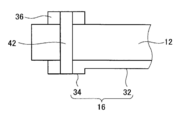
- Step B1 is a step of forming a through hole penetrating the first pad portion, the substrate, and the second pad portion. More specifically, as shown in FIG. 5, a through hole 40 that penetrates the first pad portion 34, the substrate 12, and the second pad portion 36 is formed.
- FIG. 5 corresponds to a partially enlarged cross-sectional view taken along the cutting line BB shown in FIG. 1 after performing the step B1.
- the method for forming the through-hole 40 is not particularly limited, and a known method such as drilling or laser processing can be employed, and laser processing is preferable from the viewpoint of productivity.
- the laser device used is not particularly limited, and examples thereof include a YAG laser device and a CO 2 laser device.
- the through hole 40 is formed by irradiating the surface of the first pad portion 34 or the second pad portion 36 with laser light from a direction perpendicular to the surface of the first pad portion 34 or the second pad portion 36. be able to.
- the laser light output conditions and the like are appropriately selected according to the material such as the first pad portion 34 or the second pad portion 36.
- the inner wall surface of the through-hole 40 may be coated with unburned residue (referred to as smear) by being irradiated with laser light, a desmear process that removes smear after laser processing is necessary. May be implemented.
- the desmear treatment may be performed using, for example, argon gas plasma using microwaves or oxygen gas plasma.
- the diameter of the through-hole to be formed is not particularly limited, but is usually smaller than the diameters of the first pad portion 34 and the second pad portion 36 in many cases.
- Step C1 fills the through hole with a conductive material to produce a through wiring that electrically connects the first pad portion and the second pad portion, includes a back side wiring and a through wiring,
- This is a step of forming the first lead wiring connected in a normal manner. More specifically, as shown in FIG. 6, the through hole 40 formed in the step B1 is filled with a conductive material, and the through wiring 42 is formed.
- the through wiring 42 serves to electrically connect the first pad portion 34 and the second pad portion 36.
- the second pad portion 36 and the back surface side wiring 16 are electrically connected.
- the first lead wiring including the back surface side wiring 16, the through wiring 42, and the second pad portion 36 is formed.
- One end of the first lead wiring is electrically connected to the first detection electrode 14, and the other end (second pad portion 36) is located on the surface side of the substrate 12.
- the kind of conductive material used is not particularly limited, and examples thereof include metal materials such as copper, silver, gold, chromium, aluminum, and nickel, conductive polymers, and carbon.
- the method for filling the conductive material is not particularly limited, and a known method can be employed. For example, a method of discharging and filling an ink (paste) containing the conductive material into a through hole by an ink jet method can be given.
- a flexible printed wiring board is usually connected to the conductive sheet obtained through the above steps.
- the flexible printed wiring board is disposed in the external conduction region G in FIG. 1, and is electrically connected to one end of the first lead-out wiring (second pad portion 36) and one end of the second lead-out wiring (pad portion not shown).
- the flexible printed wiring board is a board in which a plurality of wirings and terminals are provided on a substrate, and plays a role of connecting a conductive sheet and an external device (for example, a liquid crystal display device).
- the first detection electrode, the second detection electrode, the first lead wiring, and the second lead wiring are formed of the same metal material. If it is the said aspect, since the conductive characteristic between each electrode and wiring is the same, it is easy to control the voltage to apply.
- the conductive sheet of the present invention is used by being incorporated in a touch panel (capacitive touch panel).
- a touch panel capactive touch panel
- An operation in which the touch panel including the conductive sheet detects the input position will be described.
- the position detection driver always detects a change in electrostatic capacitance between the finger and the first detection electrode and the second detection electrode.
- the position detection driver detects a change in capacitance that is equal to or greater than a predetermined value
- the position detection driver detects a position where the change in capacitance is detected as an input position.
- the touch panel can detect the input position.
- a method for the touch panel to detect the input position either a mutual capacitance method or a self-capacitance method may be used.
- Employing the mutual capacitance method is preferable compared to the case of employing the self-capacitance method because a plurality of input positions can be detected simultaneously.
- a process A2 for forming a detection electrode and a lead-out wiring on a substrate, a process B1 for forming a through hole at a predetermined position, and conducting the through hole are conducted. And at least a step C1 of filling with a material.
- the 2nd embodiment of the manufacturing method of an electroconductive sheet has the same process as the above-mentioned 1st embodiment except process A2.
- the process A2 will be mainly described in detail.
- Step A2 forms a first detection electrode on the back surface of the substrate and a first pad portion electrically connected to an end of the first detection electrode, and a second detection electrode on the surface of the substrate, A second lead line electrically connected to the second detection electrode, and a second pad part disposed at a position facing the first pad part via the substrate, and the second pad part electrically connected to the second pad part;
- This is a step of forming a surface side wiring having a wiring portion.
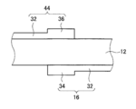
- FIG. 7 the top view of the board
- FIG. 8 is a cross-sectional view taken along the cutting line CC. As shown in FIG.
- the substrate with wiring 100 obtained by the above step A ⁇ b> 2 is electrically connected to the substrate 12, the first detection electrode 14 disposed on the back surface of the substrate 12, and the end of the first detection electrode 14.
- the first pad portion 34 connected to the substrate, the second detection electrode 18 disposed on the surface of the substrate 12, the second lead-out wiring 20, and the first pad portion 34 and the substrate 12 are disposed at positions facing each other.
- the surface side wiring 44 having the second pad portion 36 and the wiring portion 32 electrically connected to the second pad portion 36 is provided.
- the substrate with wiring 100 has the same configuration and position of the first detection electrode 14, the second detection electrode 18, and the second lead-out wiring 20, but the first It differs in the point of 1 pad part 34 and the surface side wiring 44.
- the points of the first pad portion 34 and the surface-side wiring 44 will be described in detail.
- the arrangement position of the first pad portion 34 is different from that of the first embodiment.
- the first pad portion 34 is disposed at a position that is electrically connected to the end portion of the first detection electrode 14.
- the material and size of the first pad portion 34 are as described above.
- the front surface side wiring 44 includes a second pad portion 36 disposed at a position facing the first pad portion 34 with the substrate 12 interposed therebetween, and a wiring portion 32 electrically connected to the second pad portion 36.
- the surface-side wiring 44 is electrically connected to the first detection electrode 14 through the process B1 and the process C1, and forms a first lead wiring whose one end is located on the surface side of the substrate 12. That is, the surface side wiring 44 is a part of the first lead wiring.
- the front-side wiring 44 is disposed on the substrate 12 in the outer region E O. In FIG. 7, five surface side wirings 44 are illustrated, but the number thereof is not particularly limited, and a plurality of wirings are usually arranged according to the number of detection electrodes. In FIG. 8, the heights of the wiring portion 32 and the second pad portion 36 are different, but they may be the same height. Further, in FIG. 8, the heights of the first detection electrode 14 and the first pad portion 34 are different, but they may be the same height.
- the material constituting the surface side wiring 44 is not particularly limited.
- a metal or alloy such as gold (Au), silver (Ag), copper (Cu), or aluminum (Al), ITO, tin oxide, zinc oxide, oxidation Examples thereof include metal oxides such as cadmium, gallium oxide, and titanium oxide.
- silver is preferable because of its excellent conductivity.
- the surface side wiring 44 contains a binder.
- the kind of the binder is as described above (for example, gelatin, a polymer different from gelatin, etc.).
- the 2nd pad part 36 is arrange
- the material and size of the second pad portion 36 are as described above.
- the other end of the surface side wiring 44 opposite to the second pad portion 36 side is located in the external conduction region G where a flexible printed wiring board or the like is disposed, and has a pad portion (external connection pad portion) not shown. .
- the method for forming the substrate with wiring 100 is the same as the method for forming the first embodiment. Further, by performing the above-described step B1 and step C1 on the substrate with wiring, the first pad portion, the through wiring, and the surface side wiring are included, and one end is electrically connected to the first detection electrode. A first lead wiring is formed with the other end positioned on the surface side of the substrate.
- the third embodiment of the method for manufacturing a conductive sheet for a touch panel according to the present invention includes a step A3 of forming a detection electrode and a lead wiring on a substrate, a step B1 of forming a through hole at a predetermined position, and conducting the through hole. And at least a step C1 of filling with a material.
- the 3rd embodiment of the manufacturing method of an electroconductive sheet has the same process as the said 1st embodiment except process A3.
- the process A3 will be mainly described in detail.
- Step A3 includes forming a first detection electrode on the back surface of the substrate, and a back surface side wiring having one end electrically connected to the first detection electrode and having the first pad portion on the other end, and the surface of the substrate A second detection electrode, a second lead wire electrically connected to the second detection electrode, and a second pad portion and a second pad portion arranged at positions opposed to the first pad portion through the substrate Forming a surface-side wiring having a wiring portion electrically connected to the surface.
- FIG. 9 the top view of the board
- FIG. 10 is a cross-sectional view taken along the cutting line DD. As shown in FIG.
- the substrate with wiring 200 obtained by the step A3 includes a substrate 12, a first detection electrode 14 disposed on the back surface of the substrate 12, and one end of the first detection electrode 14.
- the back-side wiring 16 that is electrically connected and has the first pad portion 34 at the other end, the second detection electrode 18 disposed on the surface of the substrate 12, the second lead-out wiring 20, and the first pad portion 34.
- a surface-side wiring 44 having a second pad portion 36 disposed at a position facing the substrate 12 and a wiring portion 32 electrically connected to the second pad portion 36.
- the first detection electrode 14, the second detection electrode 18, the back surface side wiring 16, and the second lead-out wiring 20 in the substrate with wiring 200 are the same as the members in the substrate with wiring 10 in the first embodiment, Since the surface side wiring 44 in the board
- the second pad portion 36 is disposed at a position facing the first pad portion 34, and is electrically connected through the through wiring by passing through the steps B ⁇ b> 1 and C ⁇ b> 1.
- the other end of the surface side wiring 44 opposite to the second pad portion 36 side is located in the external conduction region G where a flexible printed wiring board or the like is disposed, and has a pad portion (external connection pad portion) not shown. .
- substrate 200 with a wiring is implemented the same formation method as the said 1st embodiment.
- the backside wiring, the through wiring, and the front surface wiring are included, and one end is electrically connected to the first detection electrode.
- a first lead wiring is formed with the other end positioned on the surface side of the substrate.
- Example 1> (Preparation of silver halide emulsion) To the following 1 liquid maintained at 38 ° C. and pH 4.5, an amount corresponding to 90% of each of the following 2 and 3 liquids was simultaneously added over 20 minutes while stirring to form 0.16 ⁇ m core particles. Subsequently, the following 4 and 5 solutions were added over 8 minutes, and the remaining 10% of the following 2 and 3 solutions were added over 2 minutes to grow to 0.21 ⁇ m. Further, 0.15 g of potassium iodide was added and ripened for 5 minutes to complete the grain formation.
- the emulsion after washing with water and desalting was adjusted to pH 6.4 and pAg 7.5, and gelatin 3.9 g, sodium benzenethiosulfonate 10 mg, sodium benzenethiosulfinate 3 mg, sodium thiosulfate 15 mg and chloroauric acid 10 mg were added.
- Chemical sensitization to obtain optimum sensitivity at 0 ° C. 100 mg of 1,3,3a, 7-tetraazaindene as stabilizer and 100 mg of proxel (trade name, manufactured by ICI Co., Ltd.) as preservative It was.
- the finally obtained emulsion contains 0.08 mol% of silver iodide, and the ratio of silver chlorobromide is 70 mol% of silver chloride and 30 mol% of silver bromide. It was a silver iodochlorobromide cubic grain emulsion having a coefficient of 9%.
- Photosensitive layer forming step After a polyethylene terephthalate (PET) film having a thickness of 100 ⁇ m is subjected to corona discharge treatment, a gelatin layer having a thickness of 0.1 ⁇ m as an undercoat layer on both sides of the PET film, and an optical density of about 1.0 on the undercoat layer. And an antihalation layer containing a dye which is decolorized by alkali in the developer. On the antihalation layer, the composition for forming a photosensitive layer was applied, a gelatin layer having a thickness of 0.15 ⁇ m was further provided, and a PET film having a photosensitive layer formed on both sides was obtained. The obtained film is referred to as film A.
- the formed photosensitive layer had a silver amount of 6.0 g / m 2 and a gelatin amount of 1.0 g / m 2 .
- a high-pressure mercury lamp is used as a light source through a photomask in which a first detection electrode, a second detection electrode, a backside wiring, a second lead-out wiring, and a second pad portion are arranged on both surfaces of the film A.
- the exposure was performed using the parallel light.
- development was performed with the following developer, and further development was performed using a fixer (trade name: N3X-R for CN16X, manufactured by Fuji Film Co., Ltd.).
- a PET film in which a wiring pattern composed of Ag fine wires and a gelatin layer were formed on both surfaces was obtained.
- the gelatin layer was formed between the Ag fine wires.
- the resulting film is referred to as film B.
- Example 1 was implemented using the board
Landscapes
- Engineering & Computer Science (AREA)
- General Engineering & Computer Science (AREA)
- Theoretical Computer Science (AREA)
- Human Computer Interaction (AREA)
- Physics & Mathematics (AREA)
- General Physics & Mathematics (AREA)
- Microelectronics & Electronic Packaging (AREA)
- Manufacturing & Machinery (AREA)
- Computer Networks & Wireless Communication (AREA)
- Position Input By Displaying (AREA)
Priority Applications (2)
| Application Number | Priority Date | Filing Date | Title |
|---|---|---|---|
| CN201480021441.8A CN105190497A (zh) | 2013-04-15 | 2014-04-14 | 触控面板用导电片材的制造方法和触控面板用导电片材 |
| US14/883,339 US9891777B2 (en) | 2013-04-15 | 2015-10-14 | Method for manufacturing touch-panel conductive sheet, and touch-panel conductive sheet |
Applications Claiming Priority (2)
| Application Number | Priority Date | Filing Date | Title |
|---|---|---|---|
| JP2013-085304 | 2013-04-15 | ||
| JP2013085304A JP2014206936A (ja) | 2013-04-15 | 2013-04-15 | タッチパネル用導電シートの製造方法、および、タッチパネル用導電シート |
Related Child Applications (1)
| Application Number | Title | Priority Date | Filing Date |
|---|---|---|---|
| US14/883,339 Continuation US9891777B2 (en) | 2013-04-15 | 2015-10-14 | Method for manufacturing touch-panel conductive sheet, and touch-panel conductive sheet |
Publications (1)
| Publication Number | Publication Date |
|---|---|
| WO2014171426A1 true WO2014171426A1 (ja) | 2014-10-23 |
Family
ID=51731367
Family Applications (1)
| Application Number | Title | Priority Date | Filing Date |
|---|---|---|---|
| PCT/JP2014/060636 WO2014171426A1 (ja) | 2013-04-15 | 2014-04-14 | タッチパネル用導電シートの製造方法、および、タッチパネル用導電シート |
Country Status (5)
| Country | Link |
|---|---|
| US (1) | US9891777B2 (zh) |
| JP (1) | JP2014206936A (zh) |
| CN (1) | CN105190497A (zh) |
| TW (1) | TW201447718A (zh) |
| WO (1) | WO2014171426A1 (zh) |
Cited By (1)
| Publication number | Priority date | Publication date | Assignee | Title |
|---|---|---|---|---|
| CN104503617A (zh) * | 2014-12-26 | 2015-04-08 | 合肥鑫晟光电科技有限公司 | 触摸屏的边框结构及其制造方法、触摸屏和显示装置 |
Families Citing this family (23)
| Publication number | Priority date | Publication date | Assignee | Title |
|---|---|---|---|---|
| JP6417887B2 (ja) * | 2014-11-20 | 2018-11-07 | 日立化成株式会社 | 静電容量方式タッチパネル |
| KR102376442B1 (ko) * | 2015-01-22 | 2022-03-18 | 삼성디스플레이 주식회사 | 회로부를 포함하는 플렉서블 표시 장치 |
| CN108027675B (zh) | 2015-09-30 | 2021-10-08 | 富士胶片株式会社 | 静电电容型输入装置及其电极保护膜及其膜用组合物、转印薄膜、层叠体、图像显示装置 |
| JP6516883B2 (ja) * | 2016-01-29 | 2019-05-22 | シャープ株式会社 | アンテナデバイス |
| DE102016207387B4 (de) | 2016-04-29 | 2021-11-18 | Adidas Ag | Socke |
| CN106163103A (zh) * | 2016-07-01 | 2016-11-23 | 业成光电(深圳)有限公司 | 线路填孔搭接结构及方法 |
| JP2018017987A (ja) * | 2016-07-29 | 2018-02-01 | 株式会社ジャパンディスプレイ | 表示装置 |
| JP6768394B2 (ja) | 2016-07-29 | 2020-10-14 | 株式会社ジャパンディスプレイ | 電子機器 |
| JP2018018008A (ja) * | 2016-07-29 | 2018-02-01 | 株式会社ジャパンディスプレイ | 表示装置 |
| JP2018017988A (ja) * | 2016-07-29 | 2018-02-01 | 株式会社ジャパンディスプレイ | 表示装置 |
| CN106468972B (zh) * | 2016-08-31 | 2020-07-24 | 京东方科技集团股份有限公司 | 一种触控基板及其制造方法、触控装置 |
| CN106973495B (zh) * | 2017-05-04 | 2019-12-13 | 奇酷互联网络科技(深圳)有限公司 | 一种印刷电路板的内层电路调试方法 |
| CN107656646A (zh) * | 2017-09-27 | 2018-02-02 | 上海天马微电子有限公司 | 触摸传感器及触摸显示面板 |
| US10802315B2 (en) * | 2017-11-14 | 2020-10-13 | Japan Display, Inc. | Display device |
| CN109933227A (zh) * | 2017-12-15 | 2019-06-25 | 南昌欧菲光科技有限公司 | Fpc结构和终端 |
| JP7093190B2 (ja) * | 2018-02-01 | 2022-06-29 | 日本航空電子工業株式会社 | タッチパネル |
| JPWO2019150562A1 (ja) * | 2018-02-02 | 2021-01-28 | コニカミノルタ株式会社 | タッチパネルセンサーの製造方法及びタッチパネルセンサー基材セット |
| CN110221731B (zh) * | 2018-03-02 | 2023-03-28 | 宸鸿光电科技股份有限公司 | 触控面板的直接图案化方法及其触控面板 |
| KR102054934B1 (ko) * | 2018-05-29 | 2019-12-12 | 일진디스플레이(주) | 투명 유연 전극을 구비하는 터치패널 및 그 제조방법 |
| CN208673308U (zh) * | 2018-08-29 | 2019-03-29 | 深圳市汇顶科技股份有限公司 | 电容式悬浮触控传感器、装置及电子设备 |
| KR102453234B1 (ko) * | 2018-09-18 | 2022-10-07 | 동우 화인켐 주식회사 | 터치 센서 및 이를 포함하는 화상 표시 장치 |
| CN110333793B (zh) * | 2019-05-09 | 2022-12-09 | 业成科技(成都)有限公司 | 可挠触控结构 |
| KR102334798B1 (ko) * | 2020-12-01 | 2021-12-02 | 성균관대학교산학협력단 | 일체형 센서 모듈 및 이의 제조 방법 |
Citations (7)
| Publication number | Priority date | Publication date | Assignee | Title |
|---|---|---|---|---|
| JPH09511086A (ja) * | 1994-04-05 | 1997-11-04 | ビンステッド、ロナルド、ピーター | 多入力近接検出器およびタッチパッドシステム |
| JP2007018020A (ja) * | 2003-07-22 | 2007-01-25 | Gunze Ltd | 透明タッチパネル及び電子機器 |
| WO2008096484A1 (ja) * | 2007-02-08 | 2008-08-14 | Sharp Kabushiki Kaisha | タッチパネル装置及びその製造方法 |
| JP2009123106A (ja) * | 2007-11-16 | 2009-06-04 | Smk Corp | タッチセンサ |
| JP2009294815A (ja) * | 2008-06-04 | 2009-12-17 | Mitsubishi Electric Corp | タッチパネルおよびそれを備えた表示装置 |
| JP2011154442A (ja) * | 2010-01-26 | 2011-08-11 | Sony Corp | センサ素子及び表示装置 |
| JP2011528147A (ja) * | 2009-02-23 | 2011-11-10 | イー アンド エイチ. シーオー.,エルティーディー. | 静電容量方式のタッチスクリーンパネル |
Family Cites Families (4)
| Publication number | Priority date | Publication date | Assignee | Title |
|---|---|---|---|---|
| JP5084698B2 (ja) * | 2008-10-29 | 2012-11-28 | 京セラ株式会社 | タッチパネルおよびタッチパネル型表示装置 |
| JP5375692B2 (ja) * | 2010-03-17 | 2013-12-25 | 大日本印刷株式会社 | タッチパネルセンサの製造方法 |
| KR20120032734A (ko) * | 2010-09-29 | 2012-04-06 | 삼성모바일디스플레이주식회사 | 터치스크린패널 및 그 제조방법 |
| JP5707949B2 (ja) * | 2011-01-12 | 2015-04-30 | 大日本印刷株式会社 | タッチパネルセンサおよびタッチパネルセンサの製造方法 |
-
2013
- 2013-04-15 JP JP2013085304A patent/JP2014206936A/ja not_active Abandoned
-
2014
- 2014-04-14 WO PCT/JP2014/060636 patent/WO2014171426A1/ja active Application Filing
- 2014-04-14 CN CN201480021441.8A patent/CN105190497A/zh active Pending
- 2014-04-15 TW TW103113764A patent/TW201447718A/zh unknown
-
2015
- 2015-10-14 US US14/883,339 patent/US9891777B2/en active Active
Patent Citations (7)
| Publication number | Priority date | Publication date | Assignee | Title |
|---|---|---|---|---|
| JPH09511086A (ja) * | 1994-04-05 | 1997-11-04 | ビンステッド、ロナルド、ピーター | 多入力近接検出器およびタッチパッドシステム |
| JP2007018020A (ja) * | 2003-07-22 | 2007-01-25 | Gunze Ltd | 透明タッチパネル及び電子機器 |
| WO2008096484A1 (ja) * | 2007-02-08 | 2008-08-14 | Sharp Kabushiki Kaisha | タッチパネル装置及びその製造方法 |
| JP2009123106A (ja) * | 2007-11-16 | 2009-06-04 | Smk Corp | タッチセンサ |
| JP2009294815A (ja) * | 2008-06-04 | 2009-12-17 | Mitsubishi Electric Corp | タッチパネルおよびそれを備えた表示装置 |
| JP2011528147A (ja) * | 2009-02-23 | 2011-11-10 | イー アンド エイチ. シーオー.,エルティーディー. | 静電容量方式のタッチスクリーンパネル |
| JP2011154442A (ja) * | 2010-01-26 | 2011-08-11 | Sony Corp | センサ素子及び表示装置 |
Cited By (3)
| Publication number | Priority date | Publication date | Assignee | Title |
|---|---|---|---|---|
| CN104503617A (zh) * | 2014-12-26 | 2015-04-08 | 合肥鑫晟光电科技有限公司 | 触摸屏的边框结构及其制造方法、触摸屏和显示装置 |
| CN104503617B (zh) * | 2014-12-26 | 2017-10-13 | 合肥鑫晟光电科技有限公司 | 触摸屏的边框结构及其制造方法、触摸屏和显示装置 |
| US10007367B2 (en) | 2014-12-26 | 2018-06-26 | Boe Technology Group Co., Ltd. | Bezel structure of touch screen and method for manufacturing the same, touch screen and display device |
Also Published As
| Publication number | Publication date |
|---|---|
| JP2014206936A (ja) | 2014-10-30 |
| TW201447718A (zh) | 2014-12-16 |
| CN105190497A (zh) | 2015-12-23 |
| US20160034081A1 (en) | 2016-02-04 |
| US9891777B2 (en) | 2018-02-13 |
Similar Documents
| Publication | Publication Date | Title |
|---|---|---|
| WO2014171426A1 (ja) | タッチパネル用導電シートの製造方法、および、タッチパネル用導電シート | |
| JP5849059B2 (ja) | タッチパネル用導電性フィルムおよびタッチパネル | |
| JP5676225B2 (ja) | 導電シート、導電シートの使用方法及び静電容量方式タッチパネル | |
| JP5318998B2 (ja) | 導電シート及びタッチパネル | |
| JP5840096B2 (ja) | 導電フィルムおよびタッチパネル | |
| JP5827749B2 (ja) | 静電容量式タッチパネルおよびその製造方法、入力デバイス | |
| WO2012157555A1 (ja) | 導電シート及びタッチパネル | |
| JP5638027B2 (ja) | 導電シート及び静電容量方式タッチパネル | |
| WO2016038940A1 (ja) | タッチパネル用導電フィルムおよびタッチパネル | |
| JP6253448B2 (ja) | 導電性フィルムシート | |
| JP6009488B2 (ja) | シート状導電体、およびこれを用いるタッチパネル | |
| WO2013168698A1 (ja) | 導電性フイルム | |
| JP2011113149A (ja) | 導電シート、導電シートの使用方法及び静電容量方式タッチパネル | |
| JP5840163B2 (ja) | タッチパネルおよび保護層形成用樹脂組成物 | |
| JP5827817B2 (ja) | 導電シート、導電シートの製造方法、及び導電シートを用いた静電容量方式のタッチパネル | |
| JP6106734B2 (ja) | タッチパネル用導電性フィルムおよびタッチパネル | |
| JP5476237B2 (ja) | タッチパネル及び導電シート | |
| JP6295375B2 (ja) | タッチパネル用導電フィルムの端子接続構造およびタッチパネル | |
| JP5463315B2 (ja) | 電極シート、電極シートの製造方法、及びタッチパネル |
Legal Events
| Date | Code | Title | Description |
|---|---|---|---|
| WWE | Wipo information: entry into national phase |
Ref document number: 201480021441.8 Country of ref document: CN |
|
| 121 | Ep: the epo has been informed by wipo that ep was designated in this application |
Ref document number: 14785556 Country of ref document: EP Kind code of ref document: A1 |
|
| NENP | Non-entry into the national phase |
Ref country code: DE |
|
| 122 | Ep: pct application non-entry in european phase |
Ref document number: 14785556 Country of ref document: EP Kind code of ref document: A1 |