WO2014162923A1 - 発電装置及びその製造方法 - Google Patents
発電装置及びその製造方法 Download PDFInfo
- Publication number
- WO2014162923A1 WO2014162923A1 PCT/JP2014/058257 JP2014058257W WO2014162923A1 WO 2014162923 A1 WO2014162923 A1 WO 2014162923A1 JP 2014058257 W JP2014058257 W JP 2014058257W WO 2014162923 A1 WO2014162923 A1 WO 2014162923A1
- Authority
- WO
- WIPO (PCT)
- Prior art keywords
- region
- electrode
- piezoelectric film
- deformation
- compression
- Prior art date
- Legal status (The legal status is an assumption and is not a legal conclusion. Google has not performed a legal analysis and makes no representation as to the accuracy of the status listed.)
- Ceased
Links
Images





Classifications
-
- H—ELECTRICITY
- H02—GENERATION; CONVERSION OR DISTRIBUTION OF ELECTRIC POWER
- H02N—ELECTRIC MACHINES NOT OTHERWISE PROVIDED FOR
- H02N2/00—Electric machines in general using piezoelectric effect, electrostriction or magnetostriction
- H02N2/18—Electric machines in general using piezoelectric effect, electrostriction or magnetostriction producing electrical output from mechanical input, e.g. generators
-
- H—ELECTRICITY
- H10—SEMICONDUCTOR DEVICES; ELECTRIC SOLID-STATE DEVICES NOT OTHERWISE PROVIDED FOR
- H10N—ELECTRIC SOLID-STATE DEVICES NOT OTHERWISE PROVIDED FOR
- H10N30/00—Piezoelectric or electrostrictive devices
- H10N30/01—Manufacture or treatment
- H10N30/06—Forming electrodes or interconnections, e.g. leads or terminals
-
- H—ELECTRICITY
- H10—SEMICONDUCTOR DEVICES; ELECTRIC SOLID-STATE DEVICES NOT OTHERWISE PROVIDED FOR
- H10N—ELECTRIC SOLID-STATE DEVICES NOT OTHERWISE PROVIDED FOR
- H10N30/00—Piezoelectric or electrostrictive devices
- H10N30/01—Manufacture or treatment
- H10N30/06—Forming electrodes or interconnections, e.g. leads or terminals
- H10N30/067—Forming single-layered electrodes of multilayered piezoelectric or electrostrictive parts
-
- H—ELECTRICITY
- H10—SEMICONDUCTOR DEVICES; ELECTRIC SOLID-STATE DEVICES NOT OTHERWISE PROVIDED FOR
- H10N—ELECTRIC SOLID-STATE DEVICES NOT OTHERWISE PROVIDED FOR
- H10N30/00—Piezoelectric or electrostrictive devices
- H10N30/01—Manufacture or treatment
- H10N30/07—Forming of piezoelectric or electrostrictive parts or bodies on an electrical element or another base
- H10N30/074—Forming of piezoelectric or electrostrictive parts or bodies on an electrical element or another base by depositing piezoelectric or electrostrictive layers, e.g. aerosol or screen printing
-
- H—ELECTRICITY
- H10—SEMICONDUCTOR DEVICES; ELECTRIC SOLID-STATE DEVICES NOT OTHERWISE PROVIDED FOR
- H10N—ELECTRIC SOLID-STATE DEVICES NOT OTHERWISE PROVIDED FOR
- H10N30/00—Piezoelectric or electrostrictive devices
- H10N30/30—Piezoelectric or electrostrictive devices with mechanical input and electrical output, e.g. functioning as generators or sensors
-
- H—ELECTRICITY
- H10—SEMICONDUCTOR DEVICES; ELECTRIC SOLID-STATE DEVICES NOT OTHERWISE PROVIDED FOR
- H10N—ELECTRIC SOLID-STATE DEVICES NOT OTHERWISE PROVIDED FOR
- H10N30/00—Piezoelectric or electrostrictive devices
- H10N30/50—Piezoelectric or electrostrictive devices having a stacked or multilayer structure
- H10N30/508—Piezoelectric or electrostrictive devices having a stacked or multilayer structure adapted for alleviating internal stress, e.g. cracking control layers
-
- H—ELECTRICITY
- H10—SEMICONDUCTOR DEVICES; ELECTRIC SOLID-STATE DEVICES NOT OTHERWISE PROVIDED FOR
- H10N—ELECTRIC SOLID-STATE DEVICES NOT OTHERWISE PROVIDED FOR
- H10N30/00—Piezoelectric or electrostrictive devices
- H10N30/80—Constructional details
- H10N30/87—Electrodes or interconnections, e.g. leads or terminals
- H10N30/871—Single-layered electrodes of multilayer piezoelectric or electrostrictive devices, e.g. internal electrodes
Definitions
- the present invention relates to a power generation device including an elastic body and a method for manufacturing the elastic body.
- Patent Document 1 discloses a conventional power generator.
- the power generation device includes a flat plate-like piezoelectric substrate, a common electrode formed on one side surface of the piezoelectric substrate, and a divided electrode divided into two formed on the other side surface.
- Each divided electrode has a detection unit and a lead-out unit that is continuous with the detection unit.
- the detection unit has a very large area compared to the lead-out unit.
- the detection unit since the detection unit has a very large area as compared with the lead-out unit, charge cancellation can be suppressed and electric power can be output. For this reason, according to the pressure detector using the electric power generating apparatus of patent document 1, a detection sensitivity can be made high.
- the detection unit and the drawer unit are continuously formed. For this reason, the charge generated in the detection unit and the charge generated in the lead-out unit cancel each other. Therefore, the power generation device cannot effectively output power that can be generated by the piezoelectric substrate.
- the present invention has been made in view of the above-described conventional situation, and provides a power generation apparatus including an elastic body capable of obtaining a large power generation, and a method for manufacturing the elastic body.
- An aspect of the present invention is a power generation apparatus, which is disposed along a first surface of a base material having elasticity that causes compression deformation and tensile deformation on a first surface by receiving an external force.
- a piezoelectric film having a compression region that compresses and deforms corresponding to the deformation of the piezoelectric film, a first electrode that is in contact with the second surface of the piezoelectric film near the substrate, and a second electrode of the piezoelectric film.
- the first electrode and the second electrode can be divided at the boundary between the compression region and the tension region.
- electric charges having different polarities can be output from the respective regions without canceling out charges generated in the compression region and charges generated in the tensile region due to the piezoelectric effect of the piezoelectric film.
- a large power generation can be obtained by rectifying and synthesizing the electric power output from each region of the piezoelectric film.
- the first electrode and the second electrode can be divided at the boundary between the compression region and the tension region.
- the piezoelectric film can also be divided at the boundary between the compression region and the tension region. Also in these cases, electric power having different polarities can be output from each region without canceling out charges generated in the compression region and charges generated in the tensile region due to the piezoelectric effect of the piezoelectric film. A large power generation can be obtained by rectifying and synthesizing the electric power output from each region of the piezoelectric film.
- a laminate in which the first electrode, the piezoelectric film, and the second electrode are laminated in this order is created, and the laminate is cut into a shape that matches the compression region and the tensile region, An elastic body can be formed by sticking on top. Further, a plurality of laminated bodies may be laminated.
- the piezoelectric film can have opposite polarities in the compression region and the tension region.
- the electric charges generated on the same surface in the compression region and the tensile region due to the piezoelectric effect of the piezoelectric film can have the same polarity.
- the elastic body itself can synthesize and output charges of the same polarity generated in the compression region and the tension region without canceling out the charges generated in the compression region and the tension region. Power generation can be obtained.
- the charge may be output only from the compression region.
- the first electrode is formed on the substrate, and the piezoelectric film generating paint is applied on the first electrode while reversing the external electric field between the compression region and the tension region, A piezoelectric film having opposite polarities in the compression region and the tensile region is formed on the first electrode, the second electrode is formed on the piezoelectric film, and a take-out portion is formed at the end of the second electrode. It can be formed to extend outward from the edge. In this case, an elastic body having a piezoelectric film having opposite polarities in the compression region and the tensile region can be easily manufactured.
- one of the central portion and the outer portion of the elastic body may be a compression region, and the other may be a tensile region.
- the compression region and the tensile region are divided into a central portion and an outer portion of the base material.
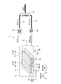
- a power generation device 1 includes an elastic body 10 having a base material 20, a first electrode 30, a piezoelectric film 40, and a second electrode 50, as shown in FIG.
- the substrate 20 is made of glass, resin, metal, or the like, and a material used as a building material can be applied.
- the base material 20 is elastic and receives an external force, so that the first surface (the upper surface of the base material 20 in FIG. 1) receives a compressive deformation with a concave deformation direction and a tensile deformation with a convex deformation direction. Will occur.
- FIG. 1 schematically shows the elastic body 10.
- the first electrode 30 is divided at the boundary between the portion of the base material 20 that undergoes compressive deformation and the portion that undergoes tensile deformation. That is, the piezoelectric film 40 is divided at the boundary between the compression region A that compresses and deforms as the base material 20 deforms and the tensile region B that undergoes tensile deformation.
- the first electrode 30 includes a first compression region electrode 31 that expands on the base material 20 corresponding to the compression region A, and a first tensile region electrode 32 that expands on the base material 20 corresponding to the tension region B. And have.
- the first electrodes 31 and 32 extend outside from the edge of the piezoelectric film 40, and have a conductive extraction portion 31A made of copper or the like connected to conductive wires 71 and 72 connected to rectifier circuits 61 and 62 described later. 32A and a conductive contact portion 31B formed of a conductive resin or the like that is in contact with the first surface of the piezoelectric film 40 close to the substrate 20 (in FIG. 1, the lower surface of the piezoelectric film 40; the same applies hereinafter), 32B respectively.
- the base material 20 receives an external force and undergoes compression deformation
- the compression region first electrode 31 also undergoes compression deformation.
- the tensile region first electrode 32 also undergoes tensile deformation.
- the piezoelectric film 40 is formed on the upper surface of the compression region first electrode 31 and the upper surface of the tensile region first electrode 32. That is, the piezoelectric film 40 is disposed along the first surface side of the substrate 20 with the first electrode 30 interposed therebetween, and the first electrode 30 is in contact with the first surface of the piezoelectric film 40.
- the piezoelectric film 40 has a compression region A that compresses and deforms together with the compressive deformation of the base material 20, and a tensile region B that tensilely deforms together with the tensile deformation of the base material 20.
- the piezoelectric film 40 When the piezoelectric film 40 is compressed and deformed in the compression region A to produce a piezoelectric effect, the piezoelectric film 40 has a positive charge on the first surface side and a negative surface on the second surface (the upper surface of the piezoelectric film 40 in FIG. 1; the same applies hereinafter). Charge collects. On the other hand, when the piezoelectric film 40 is subjected to tensile deformation in the tensile region B to generate a piezoelectric effect, negative charges are collected on the first surface side and positive charges are collected on the second surface side. Since the piezoelectric film 40 is an insulator, charges do not move between the compression region A and the tensile region B in the piezoelectric film 40, and charges generated by the piezoelectric effect do not cancel each other.
- the second electrode 50 is divided at the boundary between the compression region A and the tensile region B of the piezoelectric film 40, and the second electrode 51 for the compression region that expands corresponding to the compression region A on the piezoelectric film 40, and the piezoelectric And the second electrode 52 for the tensile region that expands in correspondence with the tensile region on the conductive film 40.
- These second electrodes 50 extend outward from the edge of the piezoelectric film 40, and have conductive extraction parts 51A, 52A made of copper or the like to which conductive wires 73, 74 connected to rectifier circuits 61, 62 described later are connected.
- the conductive film includes conductive contact portions 51B and 52B formed of a conductive resin or the like in contact with the second surface opposite to the first surface of the piezoelectric film 40.
- the power generation device 1 includes a first rectifier circuit 61, a second rectifier circuit 62, and a synchronization circuit 63.
- the first rectifier circuit 61 is connected to the extraction portion 31A of the compression region first electrode 31 provided in the compression region A and the extraction portion 51A of the compression region second electrode 51 by conducting wires 71 and 73, respectively.
- the second rectifier circuit 62 has conductors 72 and 74 respectively connected to an extraction portion 32A of the first electrode 32 for the tensile region provided in the tensile region B and an extraction portion 52A of the second electrode 52 for the tensile region. It is connected.
- the synchronizing circuit 63 has an input portion connected to the output portions of the first rectifier circuit 61 and the second rectifier circuit 62 by conducting wires 75 and 76.
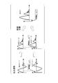
- the power generation device 1 When the base material 20 receives external force and the compressive deformation and the tensile deformation are generated on the first surface, the power generation device 1 having the above-described configuration causes the piezoelectric film 40 to be deformed along with the deformation of the base material 20 to generate a piezoelectric effect. . Then, as shown in FIG. 2, an output waveform of output 1-1 is obtained from the first electrode 31 for compression region and the second electrode 51 for compression region. Further, an output waveform of output 2-1 is obtained from the first electrode 32 for tensile region and the second electrode 52 for tensile region. The output waveform of the output 1-1 and the output waveform of the output 2-1 have a time delay ⁇ T and have a substantially opposite phase relationship.
- the power generator 1 outputs an output having a large output value by synchronizing and adding the output 1-2 output from the first rectifier circuit 61 and the output 2-2 output from the second rectifier circuit 62 by the synchronization circuit 63. 3 can be obtained.
- the power generation apparatus 1 is generated in the compression region A due to the piezoelectric effect of the piezoelectric film 40 because the first electrode 30 and the second electrode 50 are divided at the boundary between the compression region A and the tensile region B.
- a large generated power can be obtained by outputting electric power having different polarities from each region and combining them by rectification or the like without canceling out the electric charge and the electric charge generated in the tensile region B.
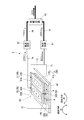
- the power generation device 2 of the present embodiment is different from the power generation device of the first embodiment in the form of the piezoelectric film 140 of the elastic body 110.
- Other configurations are the same as those of the first embodiment, and the same configurations are denoted by the same reference numerals, and detailed description thereof is omitted.
- the piezoelectric film 140 of the elastic body 110 is divided at the boundary between the compression region A and the tension region B as in the first electrode 30 and the second electrode 50.
- the elastic body 110 creates a laminated body in which the first electrode 30, the piezoelectric film 140, and the second electrode 50 are laminated in order, and the laminated body is a portion of the base material 20 that undergoes compressive deformation and a portion that undergoes tensile deformation. It can be cut in accordance with the shape and can be formed by sticking on the substrate 20.
- the power generation device 2 having the above configuration also has an output 1-1, an output 2-1, an output 1-2, an output 2-2, and an output 3, as shown in FIG. Obtainable.
- the first electrode 30, the piezoelectric film 140, and the second electrode 50 are divided at the boundary between the compression region A and the tension region B. For this reason, the electric charges generated in the compression region A and the electric charges generated in the tensile region B are not canceled by the piezoelectric effect of the piezoelectric film 140, and electric powers having different polarities are output from the respective regions, and are rectified and synthesized. By doing so, a large power generation can be obtained.
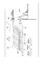
- the power generation device 3 of the present embodiment includes an elastic body 210 having a base material 20, a first electrode 230, piezoelectric films 240 ⁇ / b> A and 240 ⁇ / b> B, and a second electrode 250, and a rectifier circuit. 260.
- the base material 20 is made of glass, resin, metal, or the like, and a material used as a building material can be applied.
- the base material 20 is elastic and receives an external force, whereby the first surface (the upper surface of the base material 20 in FIG. 4) receives a compressive deformation with a concave deformation direction and a tensile deformation with a convex deformation direction. Will occur.
- FIG. 1 the first surface of the base material 20 in FIG. 4
- FIG. 4 schematically shows the elastic body 210.
- the state where compressive deformation occurs on both sides of the tensile deformation in the base material 20 is shown, but the same applies to the case where the compressive deformation and tensile deformation occur at a plurality of locations.
- the first electrode 230 extends outward from the edges of the piezoelectric films 240A and 240B, and has a conductive extraction part 231 made of copper or the like connected to a conductive wire 271 connected to a rectifier circuit 260 described later, and the piezoelectric film 240A. , 240B having a conductive contact portion 232 formed of a conductive resin or the like that is in contact with the entire first surface (the lower surfaces of the piezoelectric films 240A and 240B in FIG. Have.
- the base material 20 receives an external force and undergoes compressive deformation and tensile deformation
- the first electrode 230 also undergoes compressive deformation and tensile deformation.
- the piezoelectric films 240A and 240B are formed on the upper surface of the first electrode 230. That is, the piezoelectric films 240A and 240B are disposed along the upper surface of the base member 20, and the first electrode 230 is in contact with the first surfaces of the piezoelectric films 240A and 240B.
- the piezoelectric film 40 has a compression region A that compresses and deforms together with the compressive deformation of the base material 20, and a tensile region B that tensilely deforms together with the tensile deformation of the base material 20.
- the piezoelectric films 240A and 240B have opposite polarities in the compression region A and the tensile region B.
- the piezoelectric films 240A and 240B are also deformed together with the deformation to produce a piezoelectric effect, and all of the piezoelectric films 240A and 240B.
- positive charges are collected on the second surface side, and negative charges are collected on the first surface side. That is, in the piezoelectric films 240A and 240B, the charges do not cancel each other between the compression region A and the tension region B.
- the second electrode 250 extends outward from the edges of the piezoelectric films 240A and 240B, and has a conductive extraction part 251 made of copper or the like connected to a conductive wire 272 connected to a rectifier circuit 260 described later, and the piezoelectric film 240A. , 240B, and a conductive contact portion 252 formed from a conductive resin or the like that is in contact with the entire surface of the second surface close to the base material 20 of 240B.
- the input part of the rectifier circuit 260 is connected to the extraction part 231 of the first electrode 230 and the extraction part 251 of the second electrode 250 by conducting wires 271 and 272, respectively.
- the rectifier circuit 260 rectifies the output waveforms extracted from the extraction unit 231 of the first electrode 230 and the extraction unit 251 of the second electrode 250 and outputs an output 3 from the output unit. That is, the rectifier circuit 260 converts the negative half wave into a positive half wave.
- the power generation device 3 having the above-described configuration, when the base member 20 receives an external force, when the compressive deformation and the tensile deformation are generated on the first surface, the piezoelectric films 240A and 240B are also deformed and the piezoelectric effect is generated. At this time, the power generation device 3 can make the charges generated on the same surface side in the compression region A and the tension region B have the same polarity. For this reason, in the electric power generating apparatus 3, since the synthetic
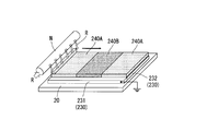
- a step of forming the first electrode 230 on the base material 20 is executed.
- the extraction portion 231 of the first electrode 230 having a rectangular parallelepiped shape that is long in the lateral direction is bonded onto the base material 20 (FIG. 5A).
- the nozzle N is moved along the direction where the extraction part 231 is extended, and the conductive resin R is apply
- a flat plate having a thickness substantially equal to the thickness of the extraction portion 231 on the base material 20 and having a length substantially equal to the length of the extraction portion 231 in the lateral direction and expanding in correspondence with the surface of the base material 20.
- the contact portion 232 of the first electrode 230 is formed.
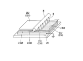
- the piezoelectric film-forming coating material P is applied onto the first electrode 230, and the compression region A and the tensile region are applied.
- a first step of forming piezoelectric films 240A and 240B having opposite polarities to B on the first electrode 230 is executed.
- the first electrode 230 is grounded, but may not be grounded.
- the voltage control device C connected to the nozzle N is controlled so that the nozzle N has a negative charge (FIGS. 6A and 6C).
- the piezoelectric film generating paint P is applied to the compression region A, an electric field from the nozzle N toward the first electrode 230 is generated.
- the piezoelectric film 240A formed by applying the piezoelectric film-generating paint P in this atmosphere is compressed and deformed, positive charges are collected on the second surface side and negative charges are collected on the first surface side of the piezoelectric film 240A. It has a certain polarity.
- a second step of forming the second electrode 250 on the piezoelectric films 240A and 240B is performed.
- the nozzle N is moved along the piezoelectric films 240A and 240B, and the conductive resin R is applied onto the piezoelectric films 240A and 240B.
- the contact portion 252 of the second electrode 250 is formed over the entire area on the piezoelectric films 240A and 240B.
- the extraction part 251 of the rectangular parallelepiped second electrode 250 that is long in the lateral direction is formed at the end of the contact part 252 of the second electrode 250 so as to extend outward from the edge of the piezoelectric films 240A and 240B.
- the elastic body 210 having the piezoelectric films 240A and 240B having opposite polarities in the compression region A and the tensile region B can be manufactured.
- the power generation device 4 includes a support portion 81 that supports the edge of the elastic body 80, as shown in FIGS. 8 to 10C.
- the support portion 81 includes a frame 81A and an elastic member 81B interposed between the frame 81A and the elastic body 80.
- the elastic body 80 is supported by the frame 81A via elastic members 81B at both end edges.
- pressure P for example, assuming an external force due to wind or the like
- the upper surface (loading surface) of the elastic body 80 is applied.
- the central portion becomes a compression region A in which the compression deformation is performed, and both end portions (outer portions) become the tension region B in which the deformation is tensile. Further, on the lower surface of the elastic body 80, the central portion becomes a tensile region B where tensile deformation is performed, and both end portions (outer portions) become compression regions A where compression deformation occurs.
- the support part 81 is provided in the both-ends edge part of the elastic body 80, the compression area
- the elastic body 90 is a rectangular flat plate, and the deformation of the elastic body 90 when an external force is applied from one surface as shown in FIG. 8 is shown. These are obtained by analysis, and in order to simplify the analysis, the elastic body 90 uses pin support by out-of-plane restraint. For this reason, the shape of a compression area
- the loading surface on which positive pressure is generated has a shape in which the upper and lower sides and the left and right sides of the rhombus are cut at the center portion of the elastic body 90 as shown in FIG.
- the region X1 is divided into a triangular region Y1 at each corner portion around the region X1, and the region X1 is a compression region that undergoes compressive deformation, and the region Y1 is a tensile region that undergoes tensile deformation.
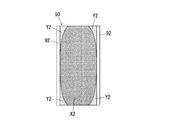
- the loading surface on which the positive pressure is generated is cut into a vertically long oval shape at the center of the elastic body 90 as shown in FIG. 9B.
- the region X2 is divided into a region X2 of the shape and the region Y2 of the outer portion around the region X2, the region X2 is a compression region that undergoes compression deformation, and the region Y2 is a tensile region that undergoes tensile deformation.
- the support portions 93 are provided at the four corners of the elastic body 90, the loading surface on which the positive pressure is generated is, as shown in FIG. 9C, a vertically long oval top and bottom and left and right regions X3.
- the region X3 is a compression region that is compressed and deformed, and the region Y3 is a tensile region that undergoes tensile deformation.
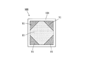
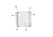
- 10A to 10C show deformation of the elastic body 100 when the elastic body 100 is a square flat plate and an external force is applied from one side as shown in FIG. These are obtained by analysis, and in order to simplify the analysis, the elastic body 100 uses pin support by out-of-plane restraint. For this reason, the shape of a compression area
- the loading surface on which positive pressure is generated has a shape in which the upper and lower sides and the left and right sides of the rhombus are cut at the center portion of the elastic body 100 as shown in FIG. 10A.
- the region X1 is divided into a triangular region Y1 at each corner around the region X1, and the region X1 is a compression region that undergoes compression deformation, and the region Y1 is a tensile region that undergoes tensile deformation.
- the support portions 102 are provided on two sides of the elastic body 100 in parallel, the loading surface on which the positive pressure is generated has a rounded corner at the center of the elastic body 100 as shown in FIG. 10B.
- the region (X2) is divided into a region X2 having a shape obtained by cutting the top and bottom of a rectangle (rounded rectangle) and a region Y2 of the outer portion around the region. .
- the loading surface on which the positive pressure is generated is, as illustrated in FIG.
- the region X3 is divided into outer regions Y3 around X3, the region X3 is a compression region in which compression deformation is performed, and the region Y3 is a tensile region in which tensile deformation is performed.
- the first electrode, the second electrode, or the piezoelectric film as described above is formed in each of the regions divided into the central portion and the outer portion of the elastic bodies 80, 90, and 100, it is generated in the compression region.
- the charges and the charges generated in the tensile region can be output effectively, and a large power generation can be obtained.
- the first electrode is provided on the base material.
- the base material is made of a metal such as aluminum and is a conductor
- the first electrode is not provided, and a conductive wire is connected to the base material. Power may be obtained. That is, when the base material is an insulator, the first electrode can be provided, and when the base material is a conductor, the base material can be used as the first electrode. Further, even when the base material is a conductor, a first electrode insulated from the base material may be provided.
- the piezoelectric film or the like is provided on one surface of the base material, but the piezoelectric film or the like may be provided on both surfaces of the base material.
- the piezoelectric film may be formed by applying a piezoelectric film-forming paint, or a film-like member may be attached.
- the degree of freedom of the shape of the piezoelectric film is expanded.
- the compression region and the tension region are divided into two to five regions, but may be divided more finely.
- the take-out portions of the first electrode and the second electrode are extended outside the edge portion of the piezoelectric film.
- the take-out portion may be positioned at the center, and therefore the take-out portion does not necessarily have to extend outward from the edge portion.
- the present invention can be used as an auxiliary power or a security sensor by being applied to a building shell such as a sash.
Landscapes
- Engineering & Computer Science (AREA)
- Manufacturing & Machinery (AREA)
- General Electrical Machinery Utilizing Piezoelectricity, Electrostriction Or Magnetostriction (AREA)
Abstract
発電装置は、外力を受けることによって第1面で圧縮変形と引張変形とが生じる弾性を有する基材と、基材の第1面に沿って配置され、基材の変形に対応して圧縮変形する圧縮領域と引張変形する引張領域とを有する圧電性膜と、圧電性膜の基材に近い第2面に接触した第1電極と、圧電性膜の第2面とは反対側の第3面に接触した第2電極と、を有する弾性体と、圧縮変形と引張変形とにより生じる圧電性膜の圧電効果によって圧縮領域に発生した電荷と引張領域に発生した電荷とが相殺し合うことなく、第1電極および第2電極からの出力を合成した電力を出力する同期回路と、を備える。
Description
本発明は弾性体を備えた発電装置及び弾性体の製造方法に関する。
本願は、2013年4月1日に、日本に出願された特願2013-076199号に基づき優先権を主張し、その内容をここに援用する。
本願は、2013年4月1日に、日本に出願された特願2013-076199号に基づき優先権を主張し、その内容をここに援用する。
特許文献1は従来の発電装置を開示している。発電装置は、平板状の圧電基板と、圧電基板の一方の側面に形成した共通電極と、他方の側面に形成した2つに分割した分割電極とを備えている。各分割電極は、検出部と、検出部に連続した引き出し部とを有している。検出部は引き出し部に比べて非常に大きい面積を有している。上記発電装置を圧力検出器に利用した場合、圧電基板は、検出部が形成されている部分で引っ張り変形し、引き出し部が形成されている部分で圧縮変形する。この際、圧電基板が検出部と引き出し部とで極性が異なった電荷を発生するため、電荷の相殺が生じる。しかし、発電装置は、検出部が引き出し部に比べて非常に大きい面積を有しているため、電荷の相殺を抑えることができ、電力を出力することができる。このため、特許文献1の発電装置を利用した圧力検出器によれば、検出感度を高くすることができる。
特許文献1の発電装置は、検出部と引き出し部とが連続して形成されている。このため、検出部で発生した電荷と、引き出し部とで発生した電荷とが相殺し合う。よって、上記発電装置では、圧電基板が発電し得る電力を有効に出力することができない。
本発明は、上記従来の実情に鑑みてなされたものであって、大きな発電力を得ることができる弾性体を備えた発電装置、及び弾性体の製造方法を提供する。
本発明の態様は、発電装置であって、外力を受けることによって第1面で圧縮変形と引張変形とが生じる弾性を有する基材と、基材の第1面に沿って配置され、基材の変形に対応して圧縮変形する圧縮領域と引張変形する引張領域とを有する圧電性膜と、圧電性膜の基材に近い第2面に接触した第1電極と、圧電性膜の第2面とは反対側の第3面に接触した第2電極とを有する弾性体と、圧縮変形と引張変形とにより生じる圧電性膜の圧電効果によって圧縮領域に発生した電荷と引張領域に発生した電荷とが相殺し合うことなく、第1電極および第2電極からの出力を合成した電力を出力する同期回路と、を備える。
上記本発明の態様によれば、圧電性膜の圧電効果によって圧縮領域に発生した電荷と引張領域に発生した電荷とが相殺し合うことなく、合成した電力を出力することができるため、大きな発電力を得ることができる。
以下、本発明における好ましい実施形態を説明する。
本実施形態の発電装置によれば、第1電極及び第2電極が、圧縮領域と引張領域との境界で分割され得る。この場合、圧電性膜の圧電効果によって圧縮領域で発生する電荷と引張領域で発生する電荷が相殺することなく、夫々の領域から極性の異なる電力を出力させることができる。そして、圧電性膜の夫々の領域から出力した電力を整流化等して合成することによって、大きな発電力を得ることができる。
本実施形態の発電装置によれば、第1電極及び第2電極が、圧縮領域と引張領域との境界で分割され得る。さらに、圧電性膜も、圧縮領域と引張領域との境界で分割され得る。これらの場合も、圧電性膜の圧電効果によって圧縮領域で発生する電荷と引張領域で発生する電荷が相殺することなく、夫々の領域から極性の異なる電力を出力させることができる。そして、圧電性膜の夫々の領域から出力した電力を整流化等して合成することによって、大きな発電力を得ることができる。また、上記構成を有する場合、第1電極、圧電性膜、及び第2電極をこの順に積層した積層体を作成し、積層体を圧縮領域及び引張領域に合わせた形状にカットして、基材上に貼着するようにして弾性体を形成することができる。また、積層体を複数積層してもよい。
本実施形態の発電装置によれば、圧電性膜が圧縮領域と引張領域とで反対の極性を有し得る。この場合、圧電性膜の圧電効果によって圧縮領域と引張領域とで同じ面に発生する電荷を同じ極性にすることができる。このため、弾性体自身が、圧縮領域と引張領域とで発生する電荷が相殺し合うことなく、圧縮領域と引張領域とで発生した同じ極性の電荷を合成して出力することができるため、大きな発電力を得ることができる。また、圧縮領域のみから電荷を出力するようにしてもよい。
本実施形態の発電装置の製造方法は、第1電極を基材上に形成し、外部電界を圧縮領域と引張領域とで反転させながら、第1電極上に圧電性膜生成塗料を塗布し、圧縮領域と引張領域とで反対の極性を有する圧電性膜を第1電極上に形成し、第2電極を圧電性膜上に形成し、第2電極の端部に取り出し部を圧電性膜の縁部より外側に延出するように形成し得る。この場合、圧縮領域と引張領域とで反対の極性を有する圧電性膜を有する弾性体を容易に製造することができる。
本実施形態の発電装置によれば、弾性体の中央部分と外側部分の一方が圧縮領域であり、他方が引張領域であり得る。この場合、発電装置が弾性体の縁部を支持する支持部を備えた建築材等に応用されると、圧縮領域と引張領域とが基材の中央部分と外側部分とに分かれて生じる。このように領域を分割して、第1電極、第2電極、又は圧電性膜を形成すると、圧縮領域に発生した電荷と引張領域に発生した電荷とを有効に出力することができ、大きな発電力を得ることができる。
次に、発電装置に係る第1~第4実施形態について、図面を参照しつつ説明する。
第1実施形態
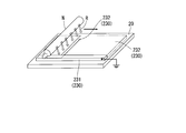
本実施形態の発電装置1は、図1に示すように、基材20、第1電極30、圧電性膜40、及び第2電極50を有する弾性体10を備えている。基材20としては、ガラス、樹脂、金属製等であり、建築材として使用される材料を適用することができる。基材20は、弾性を有し、外力を受けることによって、第一面(図1において、基材20の上面)で、変形方向が凹となる圧縮変形と、変形方向が凸となる引張変形とが生じる。図1に、弾性体10を模式的に示す。ここでは、基材20に圧縮変形と引張変形とが一箇所ずつ生じる状態を示しているが、圧縮変形及び引張変形は複数箇所に生じる場合も同様である。
本実施形態の発電装置1は、図1に示すように、基材20、第1電極30、圧電性膜40、及び第2電極50を有する弾性体10を備えている。基材20としては、ガラス、樹脂、金属製等であり、建築材として使用される材料を適用することができる。基材20は、弾性を有し、外力を受けることによって、第一面(図1において、基材20の上面)で、変形方向が凹となる圧縮変形と、変形方向が凸となる引張変形とが生じる。図1に、弾性体10を模式的に示す。ここでは、基材20に圧縮変形と引張変形とが一箇所ずつ生じる状態を示しているが、圧縮変形及び引張変形は複数箇所に生じる場合も同様である。
第1電極30は、基材20の圧縮変形する部分と引張変形する部分との境界部で分割されている。つまり、圧電性膜40が基材20の変形とともに圧縮変形する圧縮領域Aと引張変形する引張領域Bとの境界で分割されている。第1電極30は、基材20上で圧縮領域Aに対応して拡がった圧縮領域用第1電極31と、基材20上で引張領域Bに対応して拡がった引張領域用第1電極32とを有している。これら第1電極31,32は、圧電性膜40の縁部より外側に延出し、後述する整流回路61、62に連結した導線71、72を接続した銅製等の導電性を有する取出し部31A、32Aと、圧電性膜40の基材20に近い第1面(図1において、圧電性膜40の下面。以下同じ。)に接触した導電性樹脂等から形成した導電性を有する接触部31B、32Bを夫々有している。基材20が外力を受けて圧縮変形すると、それに伴って、圧縮領域用第1電極31も圧縮変形する。また、同様に、基材20が外力を受けて引張変形すると、それに伴って、引張領域用第1電極32も引張変形する。
圧電性膜40は、圧縮領域用第1電極31の上面、及び引張領域用第1電極32の上面上に形成されている。つまり、圧電性膜40は、第1電極30を挟んで基材20の第一面側に沿って配置され、第1電極30は圧電性膜40の第1面に接触している。圧電性膜40は、基材20の圧縮変形と共に圧縮変形する圧縮領域Aと、基材20の引張変形と共に引張変形する引張領域Bとを有している。圧電性膜40は、圧縮領域Aで圧縮変形して圧電効果が生じると、第1面側に正電荷、第2面(図1において、圧電性膜40の上面。以下同じ。)側に負電荷が集まる。一方、圧電性膜40は、引張領域Bで引張変形して圧電効果が生じると、第1面側に負電荷、第2面側に正電荷が集まる。圧電性膜40は、絶縁体であるため、圧電性膜40内において、圧縮領域Aと引張領域Bとの間で電荷が移動せず、圧電効果によって発生する電荷が相殺し合うことはない。
第2電極50は、圧電性膜40の圧縮領域Aと引張領域Bとの境界で分割され、圧電性膜40上で圧縮領域Aに対応して拡がった圧縮領域用第2電極51と、圧電性膜40上で引張領域に対応して拡がった引張領域用第2電極52とを有している。これら第2電極50は、圧電性膜40の縁部より外側に延出し、後述する整流回路61、62に連結した導線73、74を接続した銅製等の導電性を有する取出し部51A、52Aと、圧電性膜40の第1面とは反対側の第2面に接触した導電性樹脂等から形成した導電性を有する接触部51B、52Bとを有している。
発電装置1は、第1整流回路61、第2整流回路62、及び同期回路63を備えている。第1整流回路61は、入力部が圧縮領域Aに設けた圧縮領域用第1電極31の取出し部31Aと、圧縮領域用第2電極51の取出し部51Aの夫々に導線71、73によって接続している。第2整流回路62は、その入力部が引張領域Bに設けた引張領域用第1電極32の取出し部32Aと、引張領域用第2電極52の取出し部52Aとの夫々に導線72、74によって接続されている。同期回路63は、その入力部が第1整流回路61と第2整流回路62との夫々の出力部に導線75、76によって接続されている。
上記構成を有する発電装置1は、基材20が外力を受けることによって、第一面で圧縮変形と引張変形が生じると、基材20の変形と共に圧電性膜40も変形して圧電効果を生じる。すると、図2に示すように、圧縮領域用第1電極31及び圧縮領域用第2電極51からは出力1-1の出力波形が得られる。また、引張領域用第1電極32及び引張領域用第2電極52からは出力2-1の出力波形が得られる。出力1-1の出力波形と出力2-1の出力波形とは、時間遅れΔTを有し、略逆位相の関係である。
出力1-1を第1整流回路61で整流し、出力2-1を第2整流回路62で整流すると、第1整流回路61及び第2整流回路62の夫々からは、出力1-2及び出力2-2の出力波形が得られる。出力1-2の出力波形と出力2-2の出力波形とは、時間遅れΔTを有し、負の半波を正の半波に変換している。
第1整流回路61から出力された出力1-2と第2整流回路62から出力された出力2-2とを同期回路63で同期して加算することにより、発電装置1は出力値が大きい出力3を得ることができる。このように、発電装置1は、第1電極30及び第2電極50が圧縮領域Aと引張領域Bとの境界で分割されているため、圧電性膜40の圧電効果によって圧縮領域Aで発生する電荷と引張領域Bで発生する電荷が相殺することなく、夫々の領域から極性の異なる電力を出力させ、整流化等して合成することによって、大きな発電力を得ることができる。
第2実施形態
本実施形態の発電装置2は、図3に示すように、弾性体110の圧電性膜140の形態が第1実施形態の発電装置と相違する。他の構成は第1実施形態と同様であり、同一の構成は同一の符号を付し、詳細な説明を省略する。
本実施形態の発電装置2は、図3に示すように、弾性体110の圧電性膜140の形態が第1実施形態の発電装置と相違する。他の構成は第1実施形態と同様であり、同一の構成は同一の符号を付し、詳細な説明を省略する。
本発電装置2において、弾性体110の圧電性膜140は、第1電極30及び第2電極50と同様に圧縮領域Aと引張領域Bとの境界で分割されている。このため、弾性体110は、第1電極30、圧電性膜140、及び第2電極50を順に積層した積層体を作成し、積層体を基材20の圧縮変形する部分と引張変形する部分の形状に合わせてカットし、基材20上に貼着して形成することができる。
上記構成を有する発電装置2も、第1実施形態の発電装置1と同様、図2に示すように、出力1-1、出力2-1、出力1-2、出力2-2、出力3を得ることができる。このように、発電装置2は、第1電極30、圧電性膜140、及び第2電極50が圧縮領域Aと引張領域Bとの境界で分割されている。このため、圧電性膜140の圧電効果によって圧縮領域Aで発生する電荷と引張領域Bで発生する電荷が相殺することなく、夫々の領域から極性の異なる電力を出力させ、整流化等して合成することによって、大きな発電力を得ることができる。
第3実施形態
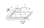
本実施形態の発電装置3は、図4に示すように、基材20、第1電極230、圧電性膜240A、240B、及び第2電極250を有する弾性体210と、整流回路260とを備えている。基材20は、ガラス、樹脂、金属製等であり、建築材として使用される材料を適用することができる。基材20は、弾性を有し、外力を受けることによって、第一面(図4において、基材20の上面)で、変形方向が凹となる圧縮変形と、変形方向が凸となる引張変形とが生じる。図4に、弾性体210を模式的に示す。ここでは、基材20に引張変形の両側に圧縮変形が生じる状態を示しているが、圧縮変形及び引張変形は複数箇所に生じる場合も同様である。
本実施形態の発電装置3は、図4に示すように、基材20、第1電極230、圧電性膜240A、240B、及び第2電極250を有する弾性体210と、整流回路260とを備えている。基材20は、ガラス、樹脂、金属製等であり、建築材として使用される材料を適用することができる。基材20は、弾性を有し、外力を受けることによって、第一面(図4において、基材20の上面)で、変形方向が凹となる圧縮変形と、変形方向が凸となる引張変形とが生じる。図4に、弾性体210を模式的に示す。ここでは、基材20に引張変形の両側に圧縮変形が生じる状態を示しているが、圧縮変形及び引張変形は複数箇所に生じる場合も同様である。
第1電極230は、圧電性膜240A、240Bの縁部より外側に延出し、後述する整流回路260に連結した導線271を接続した銅製等の導電性を有する取出し部231と、圧電性膜240A、240Bの基材20に近い第1面(図4において、圧電性膜240A、240Bの下面。以下同じ。)の全面に接触した導電性樹脂等から形成した導電性を有する接触部232とを有している。基材20が外力を受けて圧縮変形及び引張変形をすると、それに伴って、第1電極230も圧縮変形及び引張変形する。
圧電性膜240A、240Bは、第1電極230の上面上に形成されている。つまり、圧電性膜240A、240Bは、基材20の上面に沿って配置され、第1電極230は圧電性膜240A、240Bの第1面に接触している。圧電性膜40は、基材20の圧縮変形と共に圧縮変形する圧縮領域Aと、基材20の引張変形と共に引張変形する引張領域Bとを有している。圧電性膜240A、240Bは、圧縮領域Aと引張領域Bとで反対の極性を有している。つまり、圧縮領域Aでは、圧縮変形すると、圧電性膜240Aの第2面(図4において、圧電性膜240Aの上面。以下同じ。)側に正電荷、第1面側に負電荷が集まるような極性を有した圧電性膜240Aが配置されている。一方、引張領域Bでは、引張変形すると、圧電性膜240Bの第2面(図4において、圧電性膜240Bの上面。以下同じ。)側に正電荷、第1面側に負電荷が集まるような極性を有した圧電性膜240Bが配置されている。このため、基材20が外力を受けることによって、一面で圧縮変形と引張変形が生じると、その変形と共に圧電性膜240A、240Bも変形して圧電効果を生じ、圧電性膜240A、240Bの全領域において第2面側に正電荷が集まり、第1面側に負電荷が集まる。つまり、圧電性膜240A、240Bでは、圧縮領域Aと引張領域Bとの間で電荷が相殺し合うことはない。
第2電極250は、圧電性膜240A、240Bの縁部より外側に延出し、後述する整流回路260に連結した導線272を接続した銅製等の導電性を有する取出し部251と、圧電性膜240A、240Bの基材20に近い第2面の全面に接触した導電性樹脂等から形成した導電性を有する接触部252とを有している。
整流回路260は、その入力部が第1電極230の取出し部231と、第2電極250の取出し部251の夫々に導線271、272によって接続されている。整流回路260は、第1電極230の取出し部231と第2電極250の取出し部251から取り出した出力波形を整流し、出力部から出力3を出力する。つまり、整流回路260は負の半波を正の半波に変換している。
上記構成を有する発電装置3は、基材20が外力を受けることによって、第一面で圧縮変形と引張変形が生じると、その変形と共に圧電性膜240A、240Bも変形して圧電効果を生じる。この際、発電装置3は、圧縮領域Aと引張領域Bとで同じ面側に発生する電荷を同じ極性にすることができる。このため、発電装置3では、圧縮領域Aと引張領域Bとで発生する電荷が相殺し合うことなく、合成した電力を出力することができるため、大きな発電力を得ることができる。
次に、弾性体10の製造方法を説明する。
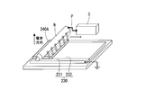
先ず、図5A、5Bに示すように、第1電極230を基材20上に形成する工程を実行する。本工程では、横方向に長い直方体形状の第1電極230の取出し部231を基材20上に接着する(図5A)。そして、取出し部231が延びている方向に沿って、ノズルNを移動し、導電性樹脂Rを基材20上に塗布する(図5B)。これによって、基材20上に取出し部231の厚さと略等しい厚さであり、取出し部231の横方向の長さと略等しい長さを有し、基材20の面に対応して拡がった平板状の第1電極230の接触部232を形成する。
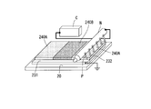
次に、図6A~6Dに示すように、外部電界を圧縮領域Aと引張領域Bとで反転させながら、第1電極230上に圧電性膜生成塗料Pを塗布し、圧縮領域Aと引張領域Bとで反対の極性を有する圧電性膜240A、240Bを第1電極230上に形成する第1工程を実行する。第1工程を実行する際、第1電極230はアースされているが、アースしされていなくてもよい。
第1工程において、圧縮領域Aに圧電性膜生成塗料Pを塗布する際は、ノズルNが負の電荷を有するようにノズルNに連結した電圧制御装置Cを制御する(図6A、6C)。これによって、圧縮領域Aに圧電性膜生成塗料Pを塗布する際は、ノズルNから第1電極230方向への電界が生成される。この雰囲気下で圧電性膜生成塗料Pを塗布して形成された圧電性膜240Aは、圧縮変形すると、圧電性膜240Aの第2面側に正電荷、第1面側に負電荷が集まるような極性を有するものになる。
一方、引張領域Bに圧電性膜生成塗料Rを塗布する際は、ノズルNが正の電荷を有するようにノズルNに連結した電圧制御装置Cを制御する(図6B)。これによって、引張領域Bに圧電性膜生成塗料Rを塗布する際は、第1電極230方向からノズルN方向への電界が生成される。この雰囲気下で圧電性膜生成塗料Pを塗布して形成された圧電性膜240Bは、引張変形すると、圧電性膜240Bの第2面側に正電荷、第1面側に負電荷が集まるような極性を有する。
次に、図7A~7Cに示すように、第2電極250を圧電性膜240A、240B上に形成する第2工程を実行する。第2工程は、圧電性膜240A、240B上に沿って、ノズルNを移動し、導電性樹脂Rを圧電性膜240A、240B上に塗布する。これによって、圧電性膜240A、240B上の全域に第2電極250の接触部252を形成する。そして、第2電極250の接触部252の端部に横方向に長い直方体形状の第2電極250の取り出し部251を圧電性膜240A、240Bの縁部より外側に延出するように形成する。このようにして、圧縮領域Aと引張領域Bとで反対の極性を有する圧電性膜240A、240Bを有する弾性体210を製造することができる。
第4実施形態
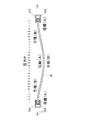
本実施形態の発電装置4は、図8~10Cに示すように、弾性体80の縁部を支持する支持部81を備えている。図8では、支持部81が、フレーム81Aと、フレーム81Aと弾性体80との間に介在する弾性部材81Bとを有している。弾性体80は、両端縁部に弾性部材81Bを介してフレーム81Aに支持されている。弾性体80の第一面(図8において、弾性体10の上面)に上方から下方に向けた圧力P(例えば、風等による外力を想定する)がかかると、弾性体80の上面(載荷面)では、中央部分が圧縮変形する圧縮領域Aになり、両端部(外側部分)が引張変形する引張領域Bになる。また、弾性体80の下面では、中央部分が引張変形する引張領域Bになり、両端部(外側部分)が圧縮変形する圧縮領域Aになる。このように、弾性体80の両端縁部に支持部81を備えると、圧縮領域Aと引張領域Bとが弾性体80の中央部分と外側部分とに分かれて生じる。
本実施形態の発電装置4は、図8~10Cに示すように、弾性体80の縁部を支持する支持部81を備えている。図8では、支持部81が、フレーム81Aと、フレーム81Aと弾性体80との間に介在する弾性部材81Bとを有している。弾性体80は、両端縁部に弾性部材81Bを介してフレーム81Aに支持されている。弾性体80の第一面(図8において、弾性体10の上面)に上方から下方に向けた圧力P(例えば、風等による外力を想定する)がかかると、弾性体80の上面(載荷面)では、中央部分が圧縮変形する圧縮領域Aになり、両端部(外側部分)が引張変形する引張領域Bになる。また、弾性体80の下面では、中央部分が引張変形する引張領域Bになり、両端部(外側部分)が圧縮変形する圧縮領域Aになる。このように、弾性体80の両端縁部に支持部81を備えると、圧縮領域Aと引張領域Bとが弾性体80の中央部分と外側部分とに分かれて生じる。
また、図9A~9Cでは、弾性体90が長方形状の平板であり、一面から図8に示すように外力を与えた際の弾性体90の変形を示している。これらは、解析によって求められており、解析を簡略化するために弾性体90においては面外方向拘束によるピン支持としている。このため、支持条件によって、圧縮領域と引張領域の形状は多少変化する。
弾性体90の縁部全周に支持部91を設けた場合、正の圧力が生じた載荷面は、図9Aに示すように、弾性体90の中央部にひし形の上下及び左右をカットした形状の領域X1と、その周囲の各コーナー部に三角形の領域Y1とに分割され、領域X1が圧縮変形する圧縮領域であり、領域Y1が引張変形する引張領域である。弾性体90の長辺の2辺に支持部92を設けた場合、正の圧力が生じた載荷面は、図9Bに示すように、弾性体90の中央部に縦長の楕円形の上下をカットした形状の領域X2とその周囲の外側部分の領域Y2とに分割され、領域X2が圧縮変形する圧縮領域であり、領域Y2が引張変形する引張領域である。弾性体90の4隅に支持部93を設けた場合、正の圧力が生じた載荷面は、図9Cに示すように、中央部に縦長の楕円形の上下及び左右をカットした形状の領域X3と、その左右の外側部分の領域Y3に分割され、領域X3が圧縮変形する圧縮領域であり、領域Y3が引張変形する引張領域である。
また、図10A~10Cは、弾性体100が正方形状の平板であり、一側面から図8に示すように外力を与えた際の弾性体100の変形を示している。これらは、解析によって求められており、解析を簡略化するために弾性体100においては面外方向拘束によるピン支持としている。このため、支持条件によって、圧縮領域と引張領域の形状は多少変化する。
弾性体100の全周縁部に支持部101を設けた場合、正の圧力が生じた載荷面は、図10Aに示すように、弾性体100の中央部にひし形の上下及び左右をカットした形状の領域X1と、その周囲の各コーナー部に三角形の領域Y1とに分割され、領域X1が圧縮変形する圧縮領域であり、領域Y1が引張変形する引張領域である。弾性体100の平行な位置にある2辺に支持部102を設けた場合、正の圧力が生じた載荷面は、図10Bに示すように、弾性体100の中央部に角部が丸くなった長方形(角丸長方形)の上下をカットした形状の領域X2とその周囲の外側部分の領域Y2とに分割され、領域X2が圧縮変形する圧縮領域であり、領域Y2が引張変形する引張領域である。弾性体100の4隅に支持部103を設けた場合、正の圧力が生じた載荷面は、図10Cに示すように、中央部に円形の上下及び左右をカットした形状の領域X3と、領域X3の周囲の外側部分の領域Y3に分割され、領域X3が圧縮変形する圧縮領域であり、領域Y3が引張変形する引張領域である。
このように、弾性体80、90、100の中央部分と外側部分に分割した領域の夫々に、上述したような第1電極、第2電極、又は圧電性膜を形成すると、圧縮領域に発生した電荷と引張領域に発生した電荷とを有効に出力することができ、大きな発電力を得ることができる。
本発明は上記記述及び図面によって説明した実施形態に限定されるものではなく、例えば次のような実施形態も本発明の技術的範囲に含まれる。
第1~第3実施形態では、基材上に第1電極を設けたが、基材がアルミ等の金属製で導電体である場合は第1電極を設けず、基材に導線を接続して電力を得てもよい。つまり、基材が絶縁体の場合は第1電極を設け、基材が導電体の場合は基材を第1電極として利用することができる。また、基材が導電体の場合でも、基材と絶縁した第1電極を設けてもよい。
第1~第3実施形態では、基材の一面に圧電性膜等を設けたが、基材の両面に圧電性膜などを設けてもよい。
圧電性膜は、第3実施形態で示したように、圧電性膜生成塗料を塗布して形成してもよいし、フィルム状の部材を張り付けてもよい。圧電性膜生成塗料を塗布して圧電性膜を形成する場合は、圧電性膜の形状の自由度が拡大する。
第4実施形態では、圧縮領域と引張領域とを2~5つの領域に分割したが、より細かく分割してもよい。
第1~第3実施形態では、第1電極及び第2電極の取出し部を圧電性膜の縁部より外側に延出させている。しかし、弾性体の形状等によっては取出し部を中心部に位置させることもあり得るため、必ずしも取出し部を縁部より外側に延出させなくてもよい。
第1~第3実施形態では、基材上に第1電極を設けたが、基材がアルミ等の金属製で導電体である場合は第1電極を設けず、基材に導線を接続して電力を得てもよい。つまり、基材が絶縁体の場合は第1電極を設け、基材が導電体の場合は基材を第1電極として利用することができる。また、基材が導電体の場合でも、基材と絶縁した第1電極を設けてもよい。
第1~第3実施形態では、基材の一面に圧電性膜等を設けたが、基材の両面に圧電性膜などを設けてもよい。
圧電性膜は、第3実施形態で示したように、圧電性膜生成塗料を塗布して形成してもよいし、フィルム状の部材を張り付けてもよい。圧電性膜生成塗料を塗布して圧電性膜を形成する場合は、圧電性膜の形状の自由度が拡大する。
第4実施形態では、圧縮領域と引張領域とを2~5つの領域に分割したが、より細かく分割してもよい。
第1~第3実施形態では、第1電極及び第2電極の取出し部を圧電性膜の縁部より外側に延出させている。しかし、弾性体の形状等によっては取出し部を中心部に位置させることもあり得るため、必ずしも取出し部を縁部より外側に延出させなくてもよい。
本発明は、サッシ等の建築外皮に応用して、補助電力もしくは防犯センサーとして利用可能である。
1、2、3 発電装置
10、80、90、100、110、210 弾性体
20 基材
30、230 第1電極
40、140、240A、240B 圧電性膜
50、250 第2電極
81、91、92、93、101、102、103 支持部
A 圧縮領域
B 引張領域
10、80、90、100、110、210 弾性体
20 基材
30、230 第1電極
40、140、240A、240B 圧電性膜
50、250 第2電極
81、91、92、93、101、102、103 支持部
A 圧縮領域
B 引張領域
Claims (7)
- 外力を受けることによって第1面で圧縮変形と引張変形とが生じる弾性を有する基材と、
前記基材の前記第1面に沿って配置され、前記基材の変形に対応して圧縮変形する圧縮領域と引張変形する引張領域とを有する圧電性膜と、
前記圧電性膜の前記基材に近い第2面に接触した第1電極と、
前記圧電性膜の前記第2面とは反対側の第3面に接触した第2電極と、
を有する弾性体と、
前記圧縮変形と前記引張変形とにより生じる前記圧電性膜の圧電効果によって前記圧縮領域に発生した電荷と前記引張領域に発生した電荷とが相殺し合うことなく、前記第1電極および前記第2電極からの出力を合成した電力を出力する同期回路と、
を備える発電装置。 - 前記第1電極及び前記第2電極が、前記圧縮領域と前記引張領域との境界で分割されている、請求項1記載の発電装置。
- 前記圧電性膜が、前記圧縮領域と前記引張領域との境界で分割されている、請求項2記載の発電装置。
- 前記弾性体は、前記圧電性膜が前記圧縮領域と前記引張領域とで反対の極性を有している、請求項1~3記載の発電装置。
- 前記弾性体の中央部分が前記圧縮領域であり、外側部分が前記引張領域である、請求項1~4のいずれか1項記載の発電装置。
- 前記弾性体の中央部分が前記引張領域であり、外側部分が前記圧縮領域である、請求項1~4のいずれか1項記載の発電装置。
- 請求項1に記載の発電装置の製造方法であって、
前記第1電極を前記基材上に形成し、
外部電界を前記圧縮領域と前記引張領域とで反転させながら、前記第1電極上に圧電性膜生成塗料を塗布し、前記圧縮領域と前記引張領域とで反対の極性を有する前記圧電性膜を前記第1電極上に形成し、
前記第2電極を前記圧電性膜上に形成し、
前記第2電極の端部に取り出し部を前記圧電性膜の縁部より外側に延出するように形成する、
発電装置の製造方法。
Applications Claiming Priority (2)
| Application Number | Priority Date | Filing Date | Title |
|---|---|---|---|
| JP2013-076199 | 2013-04-01 | ||
| JP2013076199A JP6108914B2 (ja) | 2013-04-01 | 2013-04-01 | 弾性体を備えた発電装置及び弾性体の製造方法 |
Publications (1)
| Publication Number | Publication Date |
|---|---|
| WO2014162923A1 true WO2014162923A1 (ja) | 2014-10-09 |
Family
ID=51658221
Family Applications (1)
| Application Number | Title | Priority Date | Filing Date |
|---|---|---|---|
| PCT/JP2014/058257 Ceased WO2014162923A1 (ja) | 2013-04-01 | 2014-03-25 | 発電装置及びその製造方法 |
Country Status (2)
| Country | Link |
|---|---|
| JP (1) | JP6108914B2 (ja) |
| WO (1) | WO2014162923A1 (ja) |
Families Citing this family (2)
| Publication number | Priority date | Publication date | Assignee | Title |
|---|---|---|---|---|
| KR102248847B1 (ko) * | 2015-06-01 | 2021-05-06 | 삼성전자주식회사 | 에너지 수확부를 구비한 콘택트 렌즈 |
| WO2017195499A1 (ja) * | 2016-05-10 | 2017-11-16 | パナソニックIpマネジメント株式会社 | 発電装置 |
Citations (7)
| Publication number | Priority date | Publication date | Assignee | Title |
|---|---|---|---|---|
| JPH0687838U (ja) * | 1993-05-31 | 1994-12-22 | 京セラ株式会社 | 圧力検出器 |
| JPH10229684A (ja) * | 1997-02-14 | 1998-08-25 | Seiko Epson Corp | 圧電発電装置および携帯機器 |
| JPH11252944A (ja) * | 1998-03-04 | 1999-09-17 | Seiko Epson Corp | 発電装置及び電子機器 |
| JP2003164169A (ja) * | 2001-11-20 | 2003-06-06 | Michio Tsujiura | ベルト圧電発電機 |
| JP2005237156A (ja) * | 2004-02-23 | 2005-09-02 | Taiheiyo Cement Corp | 発電装置および発電システム |
| JP2008099489A (ja) * | 2006-10-13 | 2008-04-24 | Taiheiyo Cement Corp | エネルギー変換装置 |
| JP2012175017A (ja) * | 2011-02-24 | 2012-09-10 | Kayaba Ind Co Ltd | 圧電アクチュエータ |
-
2013
- 2013-04-01 JP JP2013076199A patent/JP6108914B2/ja active Active
-
2014
- 2014-03-25 WO PCT/JP2014/058257 patent/WO2014162923A1/ja not_active Ceased
Patent Citations (7)
| Publication number | Priority date | Publication date | Assignee | Title |
|---|---|---|---|---|
| JPH0687838U (ja) * | 1993-05-31 | 1994-12-22 | 京セラ株式会社 | 圧力検出器 |
| JPH10229684A (ja) * | 1997-02-14 | 1998-08-25 | Seiko Epson Corp | 圧電発電装置および携帯機器 |
| JPH11252944A (ja) * | 1998-03-04 | 1999-09-17 | Seiko Epson Corp | 発電装置及び電子機器 |
| JP2003164169A (ja) * | 2001-11-20 | 2003-06-06 | Michio Tsujiura | ベルト圧電発電機 |
| JP2005237156A (ja) * | 2004-02-23 | 2005-09-02 | Taiheiyo Cement Corp | 発電装置および発電システム |
| JP2008099489A (ja) * | 2006-10-13 | 2008-04-24 | Taiheiyo Cement Corp | エネルギー変換装置 |
| JP2012175017A (ja) * | 2011-02-24 | 2012-09-10 | Kayaba Ind Co Ltd | 圧電アクチュエータ |
Also Published As
| Publication number | Publication date |
|---|---|
| JP2014204468A (ja) | 2014-10-27 |
| JP6108914B2 (ja) | 2017-04-05 |
Similar Documents
| Publication | Publication Date | Title |
|---|---|---|
| Kajiwara et al. | Design of dielectric elastomer actuators for vibration control at high frequencies | |
| JP5411871B2 (ja) | エレクトレット電極、それを用いたアクチュエータ、振動発電器、および振動発電装置、ならびに振動発電装置を搭載した通信装置 | |
| US8549715B2 (en) | Piezoelectric microspeaker and method of fabricating the same | |
| CN205491150U (zh) | Mems麦克风 | |
| US20150125009A1 (en) | Acoustic generator, acoustic generation device, and electronic apparatus | |
| WO2014162923A1 (ja) | 発電装置及びその製造方法 | |
| US9392373B2 (en) | Acoustic generator, acoustic generation device, and electronic device | |
| Bath et al. | A novel 3D folded zigzag piezoelectric energy harvester; modeling and experiments | |
| CN205283816U (zh) | 一种mems麦克风芯片及mems麦克风 | |
| US9392372B2 (en) | Acoustic generator, acoustic generation device, and electronic device | |
| CN104768111B (zh) | 抑制偏振的扬声器装置和调整振膜平衡位置和顺性的方法 | |
| CN205211794U (zh) | 一种叠层型压电元件 | |
| WO2015105196A1 (ja) | 音響発生器,音響発生装置,電子機器 | |
| JP5878980B2 (ja) | 音響発生器、音響発生装置および電子機器 | |
| JP6247928B2 (ja) | 振動発電体 | |
| CN201491258U (zh) | 等气压驻极体背极式双振膜电声致动器 | |
| US9154885B2 (en) | Sound generator, sound generation device, and electronic apparatus | |
| KR102181387B1 (ko) | 마이크로폰 | |
| US11128957B2 (en) | Micro-speaker, speaker device and electronic apparatus | |
| US20110170729A1 (en) | Microphone | |
| CN222509521U (zh) | 扬声器 | |
| JP6379984B2 (ja) | 固定極及び電気音響変換器 | |
| CN204348331U (zh) | 一种可控吸声结构 | |
| Yamashita et al. | Flexible Film Loudspeaker Based on Piezoelectric PZT/Si Ultra-Thin MEMS Chips | |
| TWI462599B (zh) | 單一駐極體結構之耳機麥克風 |
Legal Events
| Date | Code | Title | Description |
|---|---|---|---|
| 121 | Ep: the epo has been informed by wipo that ep was designated in this application |
Ref document number: 14778481 Country of ref document: EP Kind code of ref document: A1 |
|
| NENP | Non-entry into the national phase |
Ref country code: DE |
|
| 122 | Ep: pct application non-entry in european phase |
Ref document number: 14778481 Country of ref document: EP Kind code of ref document: A1 |