WO2014157440A1 - 半導体装置製造用仮接合用積層体、および、半導体装置の製造方法 - Google Patents
半導体装置製造用仮接合用積層体、および、半導体装置の製造方法 Download PDFInfo
- Publication number
- WO2014157440A1 WO2014157440A1 PCT/JP2014/058723 JP2014058723W WO2014157440A1 WO 2014157440 A1 WO2014157440 A1 WO 2014157440A1 JP 2014058723 W JP2014058723 W JP 2014058723W WO 2014157440 A1 WO2014157440 A1 WO 2014157440A1
- Authority
- WO
- WIPO (PCT)
- Prior art keywords
- resin
- semiconductor device
- meth
- manufacturing
- ether
- Prior art date
- Legal status (The legal status is an assumption and is not a legal conclusion. Google has not performed a legal analysis and makes no representation as to the accuracy of the status listed.)
- Ceased
Links
Images




Classifications
-
- H—ELECTRICITY
- H10—SEMICONDUCTOR DEVICES; ELECTRIC SOLID-STATE DEVICES NOT OTHERWISE PROVIDED FOR
- H10P—GENERIC PROCESSES OR APPARATUS FOR THE MANUFACTURE OR TREATMENT OF DEVICES COVERED BY CLASS H10
- H10P72/00—Handling or holding of wafers, substrates or devices during manufacture or treatment thereof
- H10P72/70—Handling or holding of wafers, substrates or devices during manufacture or treatment thereof for supporting or gripping
- H10P72/74—Handling or holding of wafers, substrates or devices during manufacture or treatment thereof for supporting or gripping using temporarily an auxiliary support
-
- C—CHEMISTRY; METALLURGY
- C09—DYES; PAINTS; POLISHES; NATURAL RESINS; ADHESIVES; COMPOSITIONS NOT OTHERWISE PROVIDED FOR; APPLICATIONS OF MATERIALS NOT OTHERWISE PROVIDED FOR
- C09J—ADHESIVES; NON-MECHANICAL ASPECTS OF ADHESIVE PROCESSES IN GENERAL; ADHESIVE PROCESSES NOT PROVIDED FOR ELSEWHERE; USE OF MATERIALS AS ADHESIVES
- C09J7/00—Adhesives in the form of films or foils
- C09J7/40—Adhesives in the form of films or foils characterised by release liners
-
- H—ELECTRICITY
- H10—SEMICONDUCTOR DEVICES; ELECTRIC SOLID-STATE DEVICES NOT OTHERWISE PROVIDED FOR
- H10P—GENERIC PROCESSES OR APPARATUS FOR THE MANUFACTURE OR TREATMENT OF DEVICES COVERED BY CLASS H10
- H10P72/00—Handling or holding of wafers, substrates or devices during manufacture or treatment thereof
- H10P72/70—Handling or holding of wafers, substrates or devices during manufacture or treatment thereof for supporting or gripping
- H10P72/74—Handling or holding of wafers, substrates or devices during manufacture or treatment thereof for supporting or gripping using temporarily an auxiliary support
- H10P72/7448—Handling or holding of wafers, substrates or devices during manufacture or treatment thereof for supporting or gripping using temporarily an auxiliary support the bond interface between the auxiliary support and the wafer comprising two or more, e.g. multilayer adhesive or adhesive and release layer
-
- H—ELECTRICITY
- H10—SEMICONDUCTOR DEVICES; ELECTRIC SOLID-STATE DEVICES NOT OTHERWISE PROVIDED FOR
- H10P—GENERIC PROCESSES OR APPARATUS FOR THE MANUFACTURE OR TREATMENT OF DEVICES COVERED BY CLASS H10
- H10P95/00—Generic processes or apparatus for manufacture or treatments not covered by the other groups of this subclass
- H10P95/90—Thermal treatments, e.g. annealing or sintering
-
- C—CHEMISTRY; METALLURGY
- C09—DYES; PAINTS; POLISHES; NATURAL RESINS; ADHESIVES; COMPOSITIONS NOT OTHERWISE PROVIDED FOR; APPLICATIONS OF MATERIALS NOT OTHERWISE PROVIDED FOR
- C09J—ADHESIVES; NON-MECHANICAL ASPECTS OF ADHESIVE PROCESSES IN GENERAL; ADHESIVE PROCESSES NOT PROVIDED FOR ELSEWHERE; USE OF MATERIALS AS ADHESIVES
- C09J2203/00—Applications of adhesives in processes or use of adhesives in the form of films or foils
- C09J2203/326—Applications of adhesives in processes or use of adhesives in the form of films or foils for bonding electronic components such as wafers, chips or semiconductors
-
- C—CHEMISTRY; METALLURGY
- C09—DYES; PAINTS; POLISHES; NATURAL RESINS; ADHESIVES; COMPOSITIONS NOT OTHERWISE PROVIDED FOR; APPLICATIONS OF MATERIALS NOT OTHERWISE PROVIDED FOR
- C09J—ADHESIVES; NON-MECHANICAL ASPECTS OF ADHESIVE PROCESSES IN GENERAL; ADHESIVE PROCESSES NOT PROVIDED FOR ELSEWHERE; USE OF MATERIALS AS ADHESIVES
- C09J2301/00—Additional features of adhesives in the form of films or foils
- C09J2301/30—Additional features of adhesives in the form of films or foils characterized by the chemical, physicochemical or physical properties of the adhesive or the carrier
- C09J2301/312—Additional features of adhesives in the form of films or foils characterized by the chemical, physicochemical or physical properties of the adhesive or the carrier parameters being the characterizing feature
-
- H—ELECTRICITY
- H10—SEMICONDUCTOR DEVICES; ELECTRIC SOLID-STATE DEVICES NOT OTHERWISE PROVIDED FOR
- H10P—GENERIC PROCESSES OR APPARATUS FOR THE MANUFACTURE OR TREATMENT OF DEVICES COVERED BY CLASS H10
- H10P72/00—Handling or holding of wafers, substrates or devices during manufacture or treatment thereof
- H10P72/70—Handling or holding of wafers, substrates or devices during manufacture or treatment thereof for supporting or gripping
- H10P72/74—Handling or holding of wafers, substrates or devices during manufacture or treatment thereof for supporting or gripping using temporarily an auxiliary support
- H10P72/7412—Handling or holding of wafers, substrates or devices during manufacture or treatment thereof for supporting or gripping using temporarily an auxiliary support the auxiliary support including means facilitating the separation of a device or wafer from the auxiliary support
-
- H—ELECTRICITY
- H10—SEMICONDUCTOR DEVICES; ELECTRIC SOLID-STATE DEVICES NOT OTHERWISE PROVIDED FOR
- H10P—GENERIC PROCESSES OR APPARATUS FOR THE MANUFACTURE OR TREATMENT OF DEVICES COVERED BY CLASS H10
- H10P72/00—Handling or holding of wafers, substrates or devices during manufacture or treatment thereof
- H10P72/70—Handling or holding of wafers, substrates or devices during manufacture or treatment thereof for supporting or gripping
- H10P72/74—Handling or holding of wafers, substrates or devices during manufacture or treatment thereof for supporting or gripping using temporarily an auxiliary support
- H10P72/7416—Handling or holding of wafers, substrates or devices during manufacture or treatment thereof for supporting or gripping using temporarily an auxiliary support used during dicing or grinding
-
- H—ELECTRICITY
- H10—SEMICONDUCTOR DEVICES; ELECTRIC SOLID-STATE DEVICES NOT OTHERWISE PROVIDED FOR
- H10P—GENERIC PROCESSES OR APPARATUS FOR THE MANUFACTURE OR TREATMENT OF DEVICES COVERED BY CLASS H10
- H10P72/00—Handling or holding of wafers, substrates or devices during manufacture or treatment thereof
- H10P72/70—Handling or holding of wafers, substrates or devices during manufacture or treatment thereof for supporting or gripping
- H10P72/74—Handling or holding of wafers, substrates or devices during manufacture or treatment thereof for supporting or gripping using temporarily an auxiliary support
- H10P72/7422—Handling or holding of wafers, substrates or devices during manufacture or treatment thereof for supporting or gripping using temporarily an auxiliary support used to protect an active side of a device or wafer
-
- H—ELECTRICITY
- H10—SEMICONDUCTOR DEVICES; ELECTRIC SOLID-STATE DEVICES NOT OTHERWISE PROVIDED FOR
- H10P—GENERIC PROCESSES OR APPARATUS FOR THE MANUFACTURE OR TREATMENT OF DEVICES COVERED BY CLASS H10
- H10P72/00—Handling or holding of wafers, substrates or devices during manufacture or treatment thereof
- H10P72/70—Handling or holding of wafers, substrates or devices during manufacture or treatment thereof for supporting or gripping
- H10P72/74—Handling or holding of wafers, substrates or devices during manufacture or treatment thereof for supporting or gripping using temporarily an auxiliary support
- H10P72/744—Details of chemical or physical process used for separating the auxiliary support from a device or a wafer
Definitions
- the present invention relates to a temporary bonding laminate for manufacturing a semiconductor device and a method for manufacturing a semiconductor device.
- a wire bonding method As an electrical connection method from an integrated circuit in an IC chip to an external terminal of the IC chip, a wire bonding method has been widely known.
- a silicon substrate is used.
- a method is known in which a through-hole is provided in the semiconductor device and a metal plug as an external terminal is connected to an integrated circuit so as to pass through the through-hole (so-called silicon through electrode (TSV) forming method).
- TSV silicon through electrode
- a technique for improving the degree of integration per unit area of a silicon substrate by multilayering integrated circuits in an IC chip is known.
- the multilayered integrated circuit increases the thickness of the IC chip, it is necessary to reduce the thickness of the members constituting the IC chip.
- the thinning of the silicon substrate is being considered as the thinning of such a member, which not only leads to the miniaturization of the IC chip, but also saves labor in the through hole manufacturing process of the silicon substrate in the manufacture of the silicon through electrode. Because it is possible, it is considered promising.
- a semiconductor silicon wafer having a thickness of about 700 to 900 ⁇ m is widely known as a semiconductor silicon wafer used in a semiconductor device manufacturing process.
- the thickness of a semiconductor silicon wafer has been reduced for the purpose of miniaturizing an IC chip. Attempts have been made to reduce the thickness to 200 ⁇ m or less.
- the semiconductor silicon wafer having a thickness of 200 ⁇ m or less is very thin, and the semiconductor device manufacturing member based on this is also very thin, such a member can be further processed, or When such a member is simply moved, it is difficult to support the member stably and without causing damage.
- the wafer is supported by a support layer system, and a plasma polymer layer obtained by a plasma deposition method is interposed between the wafer and the support layer system as a separation layer.
- the adhesive bond between the support layer system and the separation layer is made larger than the bond bond between the wafer and the separation layer, so that when the wafer is detached from the support layer system, the wafer is easily detached from the separation layer.
- a technique configured to be separated is also known (see Patent Document 2).
- a pressure-sensitive adhesive film that comprises syndiotactic 1,2-polybutadiene and a photopolymerization initiator, and whose adhesive force changes upon irradiation with radiation (Patent Document 6). Further, the support substrate and the semiconductor wafer are temporarily bonded with an adhesive made of polycarbonate, the semiconductor wafer is processed, irradiated with irradiation radiation, and then heated, thereby processing the processed semiconductor wafer. A technique for detaching the substrate from the support substrate is known (Patent Document 7).
- the surface of the semiconductor wafer on which the device is provided (that is, the device surface of the device wafer) and the support substrate (carrier substrate) are temporarily bonded via a layer made of an adhesive known in Patent Document 1 or the like.
- the adhesive layer is required to have a certain degree of adhesion to stably support the semiconductor wafer. That is, in the case of temporarily adhering the entire device surface of the semiconductor wafer and the support substrate through the adhesive layer, the temporary adhesion between the semiconductor wafer and the support substrate is sufficient, and the semiconductor wafer is stably and However, the temporary adhesion between the semiconductor wafer and the support substrate is too strong, so that the device may be damaged or detached from the semiconductor wafer. Problems such as device detachment tend to occur.
- a plasma polymer layer as a separation layer is formed between the wafer and the support layer system by a plasma deposition method.
- the forming method is (1) the equipment cost for carrying out the plasma deposition method is usually high; (2) the layer formation by the plasma deposition method requires time for vacuuming and monomer deposition in the plasma apparatus; and (3) Even when a separation layer composed of a plasma polymer layer is provided, when supporting a wafer to be processed, the wafer is released from support while the adhesive bond between the wafer and the separation layer is sufficient. In such a case, it is not easy to control the adhesive bond so that the wafer is easily detached from the separation layer;
- the present invention has been made in view of the above background, and its purpose is to provide a temporary support for a member to be processed reliably and easily when a member to be processed (such as a semiconductor wafer) is subjected to mechanical or chemical treatment. And a temporary bonding laminate for manufacturing a semiconductor device, which can easily release temporary support for the processed member without damaging the processed member even after a process at a high temperature, and a semiconductor device It is to provide a manufacturing method.
- the present inventors provide a temporary bonded laminate including a release layer and an adhesive layer between a support and a member to be processed.
- ⁇ 1> A temporary junction laminate for manufacturing a semiconductor device having (A) a release layer and (B) an adhesive layer, wherein the (A) release layer has a softening point of (a1) 200 ° C. or higher.
- thermoplastic resin is at least one thermoplastic resin selected from a polyethersulfone resin, a polyimide resin, a polyester resin, a polybenzimidazole resin, a polyphenylene ether resin, a polyphenylene sulfide resin, and a polyether ketone resin ⁇ 3
- ⁇ 5> The laminate for temporary bonding for manufacturing a semiconductor device according to any one of ⁇ 1> to ⁇ 4>, wherein the resin 2 contains a thermoplastic resin selected from a polycarbonate resin, a polyurethane resin, and a hydrocarbon resin. . ⁇ 6>
- ⁇ 7> The semiconductor according to any one of ⁇ 1> to ⁇ 6>, wherein the adhesive layer (B) includes a binder, a polymerizable monomer, and at least one of a photopolymerization initiator and a thermal polymerization initiator.
- the method further includes a step of removing the temporary bonding laminate remaining on the member to be processed with a peeling solvent, ⁇ 8> or ⁇ 9>
- the peeling solvent includes at least one of a hydrocarbon solvent and an ether solvent.
- the release solvent contains at least one of cyclopentane, n-hexane, cyclohexane, n-heptane, limonene, p-menthane, tetrahydrofuran (THF), 1,3-dioxolane, and anisole.
- the member to be treated when a member to be treated is subjected to mechanical or chemical treatment, the member to be treated can be temporarily and reliably supported, and the treated member is damaged even when subjected to a process at a high temperature. It is possible to provide a temporary bonding laminated body for manufacturing a semiconductor device and a method for manufacturing a semiconductor device, which can release temporary support for a processed member without imparting.
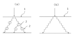
- FIG. 1A is a conceptual diagram showing a state in which a solvent permeates through a release layer in the present invention
- FIG. 1B is a conceptual diagram showing a state in which a solvent penetrates in a conventional release layer.
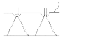
- FIG. 2 is a conceptual diagram showing a state where a solvent enters from the surface of the release layer in the present invention.
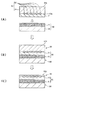
- 3A, FIG. 3B, and FIG. 3C are respectively a schematic cross-sectional view for explaining the temporary bonding between the adhesive support and the device wafer, a schematic plan view showing the device wafer temporarily bonded by the adhesive support, and the bonding. It is a schematic sectional drawing which shows the state by which the device wafer temporarily bonded by the adhesive support body was thinned.
- FIG. 1A is a conceptual diagram showing a state in which a solvent permeates through a release layer in the present invention
- FIG. 1B is a conceptual diagram showing a state in which a solvent penetrates in a conventional release layer.
- FIG. 2 is
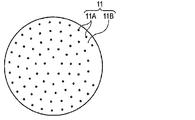
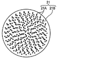
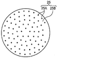
- FIG. 4 is a schematic top view of the adhesive support in the embodiment of the present invention.
- FIG. 5 is a schematic top view of the adhesive support in the embodiment of the present invention.
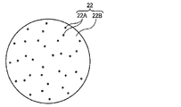
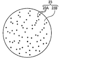
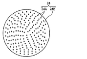
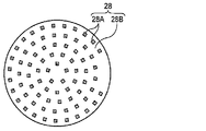
- FIG. 6 is a schematic top view of an aspect of the adhesive support in the embodiment of the present invention.
- FIG. 7 is a schematic top view of an aspect of the adhesive support in the embodiment of the present invention.
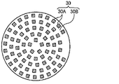
- FIG. 8 is a schematic top view of an aspect of the adhesive support in the embodiment of the present invention.
- FIG. 9 is a schematic top view of an aspect of the adhesive support in the embodiment of the present invention.
- FIG. 10 is a schematic top view of an aspect of the adhesive support in the embodiment of the present invention.
- FIG. 11 is a schematic top view of an aspect of the adhesive support in the embodiment of the present invention.
- FIG. 12 is a schematic top view of an aspect of the adhesive support in the embodiment of the present invention.
- FIG. 13 is a schematic top view in 1 aspect of the adhesive support body in embodiment of this invention.
- FIG. 14 is a schematic top view of an aspect of the adhesive support in the embodiment of the present invention.
- FIG. 15 is a schematic cross-sectional view for explaining the release of the temporarily bonded state between the conventional adhesive support and the device wafer.
- substitution and non-substitution includes those having no substituent and those having a substituent.
- the “alkyl group” includes not only an alkyl group having no substituent (unsubstituted alkyl group) but also an alkyl group having a substituent (substituted alkyl group).
- Actinic light” or “radiation” in the present specification means, for example, those including visible light, ultraviolet rays, far ultraviolet rays, electron beams, X-rays and the like. In the present invention, “light” means actinic rays or radiation.
- the term “exposure” in the present specification is not limited to exposure by far-ultraviolet rays such as mercury lamps, ultraviolet rays, and excimer lasers, X-rays, EUV light, etc. It also means drawing with particle beams.
- “(meth) acrylate” represents acrylate and methacrylate
- “(meth) acryl” represents acryl and methacryl
- “(meth) acryloyl” represents acryloyl and methacryloyl.
- “monomer” and “monomer” are synonymous.
- the monomer in the present invention is a compound having a weight average molecular weight of 2,000 or less, distinguished from oligomers and polymers.
- a polymerizable compound means a compound having a polymerizable group, and may be a monomer or a polymer, and a polymerizable group is a group involved in a polymerization reaction.
- a polymerizable group is a group involved in a polymerization reaction.
- a temporary bonding laminate for manufacturing a semiconductor device according to the present invention includes a temporary layer for manufacturing a semiconductor device having (A) a release layer and (B) an adhesive layer.
- solvent soluble (hereinafter sometimes referred to as "solvent soluble”) the resin 2.
- solvent soluble the resin 2.
- it is made easy to osmose
- FIG. 1 is a conceptual diagram showing a state in which a solvent permeates through a release layer according to the present invention and the prior art, where 1 indicates a release layer and 2 indicates a resin 2.
- straight arrows and wavy arrows in the figure indicate the permeation state of the solvent.
- FIG. 1 is a diagram for facilitating understanding of the concept of the present invention. The amount of resin 2 (2 in the figure) and the size of resin 2 (2 in the figure) in the release layer are shown in FIG. 1 is not the same (the same applies to FIG. 2 and subsequent figures).
- the release layer 1 that is, the layer mainly composed of the resin 1, has the resin 2 (2 in the figure). Although it is spherical in FIG.
- the resin 2 may exist on the surface of the release layer 1.
- the surface area through which the release layer 1 permeates the solvent increases.
- the solvent easily penetrates into the peeling layer, and the peeling layer can be peeled more easily.
- the laminated body for temporary joining for semiconductor device manufacture in this invention is demonstrated. It is preferable that the laminated body for temporary joining for semiconductor device manufacture in this invention is used for manufacture of the semiconductor device which has the process of heat-processing.
- the temporary bonding laminated body for manufacturing a semiconductor device in the present invention when a member to be processed is subjected to mechanical or chemical treatment, the member to be processed can be temporarily and reliably supported, and a process at a high temperature can be performed. Even if it passes, the laminated body for semiconductor device manufacture for temporary joining which can cancel
- the laminated body for temporary bonding for manufacturing a semiconductor device in the present invention is preferably for forming a through silicon via.
- the formation of the through silicon via will be described in detail later.
- the (A) release layer in the present invention includes (a1) a resin 1 having a softening point of 200 ° C. or higher, and (a2) a resin 2 that can be dissolved in a solvent after curing.
- Resin 1 is used for the purpose of improving the peelability of the release layer surface. Therefore, the resin 1 is required to have a small change in peelability with respect to heat.
- the softening point of the resin 1 is 200 ° C. or higher.
- the softening point is preferably 200 ° C to 450 ° C, more preferably 250 ° C to 400 ° C, and further preferably 280 ° C to 350 ° C.
- the softening point of the resin 1 represents that measured by a general method using a viscoelasticity measuring apparatus.
- the softening point of the resin 1 is measured as a temperature at which the loss tangent (tan ⁇ ) measured using a viscoelasticity measuring device under a constant temperature rise is maximized.
- the loss tangent (tan ⁇ ) is calculated by the following equation.
- G ′′ represents the loss shear modulus and G ′ represents the storage shear modulus.
- the rate of temperature rise is preferably in the range of 0.5 to 20 ° C./min, more preferably in the range of 1 to 10 ° C./min, and in the range of 2 to 5 ° C./min. Is particularly preferred.
- the resin 1 examples include olefin copolymer (for example, methylpentene copolymer), cycloolefin copolymer (for example, norbornene copolymer, dicyclopentadiene copolymer, tetracyclododecene copolymer), novolac resin, phenol Resin, epoxy resin, melamine resin, urea resin, unsaturated polyester resin, alkyd resin, polyurethane resin, solvent-soluble polyimide resin, polyethylene resin, polypropylene resin, polyvinyl chloride resin, polyvinyl acetate resin, PTFE resin, PFA resin, FEP resin, ethylene-TFE copolymer resin, PVDF resin, PCTFE resin, ethylene-CTFE resin, TFE-perfluorodimethyldioxole copolymer resin, PVF resin, ABS resin, AS resin, acrylic resin, cellulose resin Synthetic resins such as polyamide, polyacetal, polycarbonate, polyphenylene
- PTFE resin PFA resin, FEP resin, ethylene-TFE copolymer resin, PVDF resin, PCTFE resin, ethylene-CTFE resin, TFE-perfluorodimethyldioxole copolymer resin, PVF resin, polyethersulfone resin, solvent Soluble type polyimide resin, polyester resin, polybenzimidazole resin, polyphenylene ether resin, polyether ketone resin are preferable.
- PFA resin TFE-perfluorodimethyldioxole copolymer resin, PVF resin, polyethersulfone resin, solvent-soluble type Polyimide resin, polyester resin, polybenzimidazole resin, polyphenylene ether resin, polyether ketone resin are more preferable, polyethersulfone resin, solvent-soluble polyimide resin, polyester resin, poly Lens imidazole resins, polyphenylene ether resins, polyether ketone resins are particularly preferred.
- the resin 1 is preferably a thermoplastic resin, and is at least one thermoplastic resin selected from a polyethersulfone resin, a solvent-soluble polyimide resin, a polyester resin, a polybenzimidazole resin, a polyphenylene ether resin, and a polyetherketone resin. It is particularly preferred.
- the resin 1 in the present invention usually has lower solvent solubility than the resin 2.
- the resin 1 in the present invention preferably has a lower dissolution rate (mass%) of 5 to 15 mass% than the resin 2 when it is dissolved at 25 ° C. in at least one of the above specific solvents. Further, when dissolved at 25 ° C. in at least one of the above specific solvents of the resin 1, the dissolution ratio (mass%) is preferably 1 to 50 mass%.
- the resin 2 is used for the purpose of improving the removability when removing the peeling layer residue from the member to be treated with a solvent.
- Resin 2 in the present invention is cured with hexane, heptane, ethyl acetate, acetone, methanol, ethanol, isopropanol, 1,4-dioxane, tetrahydrofuran, 1-methoxy-2-propanol, 2-acetoxy-1-methoxypropane, Acetonitrile, methyl ethyl ketone, cyclohexanone, toluene, dimethyl sulfoxide, N, N-dimethylformamide, N, N-dimethylacetamide, N-methyl-2-pyrrolidinone, N-ethyl-2-pyrrolidinone, chloroform, methylene chloride, anisole, xylene, And at least one solvent selected from mesitylene contains a resin that dissolves
- the resin 2 is used to make it easier to remove the resin 1 from the member to be treated with a solvent. Therefore, the resin 2 is required to have a resin that can be dissolved in a solvent after curing.
- the solvent-soluble resin in the present invention is more preferably a resin that can be dissolved in at least one of the above solvents at 10% by mass or more at 25 ° C. With such a configuration, the removal of the release layer can be completed in a short time.
- the release layer in the present invention includes the resin 1 having a high softening point, the release layer formed only of the release layer having a high softening point has a high cohesive property peculiar to the high softening point material, so It is thought to have a long time.
- the resin 2 in the present invention may be a resin that can be dissolved in a solvent after curing, and the solvent-dissolving solubility before curing may or may not be solvent-soluble.
- the resin 2 in the present invention usually has a softening point lower than that of the resin 1.
- the softening point of the resin 2 in the present invention is preferably 20 ° C. or more lower than the softening point of the resin 1, and more preferably 50 ° C. or lower.
- any resin that can be dissolved in a solvent can be used as the resin 2.
- the total addition amount of the resin 1 and the resin 2 in the release layer of the present invention is preferably 1 to 50% by mass, more preferably 10 to 40% by mass, and more preferably 20 to 30% by mass with respect to the release layer composition used in the present invention. Is particularly preferred.
- the difference in SP value [MPa 1/2 ] between the resin 1 and the resin 2 is preferably 1 or more and less than 10, and preferably 2 or more and 9 Less than, more preferably 3 or more and less than 8.
- the total amount of the resin in the release layer of the present invention is preferably 1 to 100% by mass, more preferably 70 to 100% by mass, and more preferably 90 to 100% by mass with respect to the total solid content (excluding the solvent) of the release layer of the present invention. 100% by mass is particularly preferred.
- the release layer of the present invention may contain a resin other than the resin 1 and the resin 2 within a range not departing from the gist of the present invention, but the amount of such resin is the total resin component contained in the release layer. It is preferable that it is 5 mass% or less.
- a solvent is usually used to form a release layer. Any known solvent can be used as long as it can form a release layer, but N-methyl-2-pyrrolidone, N, N-dimethylacetamide, 2-butanone, methyl amyl ketone, anisole, xylene, and the like can be used. N-methyl-2-pyrrolidone, N, N-dimethylacetamide, methyl amyl ketone or anisole are preferred.
- the solvent is preferably used so that the solid content concentration of the release layer composition for forming the release layer is 5 to 40% by mass.
- the release layer composition may contain various additives as necessary.
- surfactants may be added to the release layer composition of the present invention from the viewpoint of further improving coatability.
- various surfactants such as a fluorine-based surfactant, a nonionic surfactant, a cationic surfactant, an anionic surfactant, and a silicone-based surfactant can be used.
- the release layer of the release layer composition of the present invention contains a fluorosurfactant, so that the liquid properties (particularly fluidity) when prepared as a coating solution are further improved.
- the uniformity and liquid-saving property can be further improved. That is, in the case of forming a film using a release layer composition containing a fluorosurfactant, the wettability to the coated surface is improved by reducing the interfacial tension between the coated surface and the coating liquid. The applicability to the coated surface is improved. For this reason, even when a thin film of about several ⁇ m is formed with a small amount of liquid, it is effective in that it is possible to more suitably form a film having a uniform thickness with small thickness unevenness.
- the fluorine content in the fluorosurfactant is preferably 3% by mass to 40% by mass, more preferably 5% by mass to 30% by mass, and particularly preferably 7% by mass to 25% by mass.
- a fluorine-based surfactant having a fluorine content within this range is effective in terms of uniformity of coating film thickness and liquid-saving properties, and has good solubility in the release layer composition.
- fluorosurfactant examples include Megafac F171, F172, F173, F176, F176, F177, F141, F142, F143, F144, R30, F437, F475, F479, F482, F554, F780, F780, F781 (above DIC Corporation), Florard FC430, FC431, FC171 (above, Sumitomo 3M Limited), Surflon S-382, SC-101, Same SC-103, Same SC-104, Same SC-105, Same SC1068, Same SC-381, Same SC-383, Same S393, Same KH-40 (manufactured by Asahi Glass Co., Ltd.), PF636, PF656, PF6320 PF6520, PF7002 (manufactured by OMNOVA), and the like.
- nonionic surfactant examples include glycerol, trimethylolpropane, trimethylolethane, and ethoxylates and propoxylates thereof (for example, glycerol propoxylate, glycerol ethoxylate, etc.), polyoxyethylene lauryl ether, polyoxyethylene Stearyl ether, polyoxyethylene oleyl ether, polyoxyethylene octylphenyl ether, polyoxyethylene nonylphenyl ether, polyethylene glycol dilaurate, polyethylene glycol distearate, sorbitan fatty acid ester (Pluronic L10, L31, L61, L62 manufactured by BASF, 10R5, 17R2, 25R2, Tetronic 304, 701, 704, 901, 904, 150R1, Rusupasu 20000 (manufactured by Nippon Lubrizol Corporation), and the like.
- cationic surfactant examples include phthalocyanine derivatives (trade name: EFKA-745, manufactured by Morishita Sangyo Co., Ltd.), organosiloxane polymer KP341 (manufactured by Shin-Etsu Chemical Co., Ltd.), (meth) acrylic acid ( Co) polymer polyflow no. 75, no. 90, no. 95 (manufactured by Kyoeisha Chemical Co., Ltd.), W001 (manufactured by Yusho Co., Ltd.) and the like.
- phthalocyanine derivatives trade name: EFKA-745, manufactured by Morishita Sangyo Co., Ltd.
- organosiloxane polymer KP341 manufactured by Shin-Etsu Chemical Co., Ltd.
- (meth) acrylic acid ( Co) polymer polyflow no. 75, no. 90, no. 95 manufactured by Kyoeisha Chemical Co., Ltd.
- W001 manufactured by Yusho Co., Ltd.
- anionic surfactants include W004, W005, W017 (manufactured by Yusho Co., Ltd.) and the like.
- silicone surfactant examples include “Toray Silicone DC3PA”, “Toray Silicone SH7PA”, “Tore Silicone DC11PA”, “Tore Silicone SH21PA”, “Tore Silicone SH28PA”, “Toray Silicone” manufactured by Toray Dow Corning Co., Ltd.
- the method for forming the release layer of the laminate for temporary bonding for manufacturing a semiconductor device according to the present invention is not particularly limited, but by appropriately changing the type and content of the resin 1 described above as preferable.
- the resin 1 and the resin 2 are selected from the above-mentioned preferred specific examples and are made to have a more preferable concentration.
- the adhesive layer is used for the purpose of bonding the release layer and the substrate. Therefore, the adhesive layer is required to have a small adhesive change with respect to heat and chemicals.
- the adhesive layer is formed on the carrier substrate by using an adhesive composition containing each component described later using a conventionally known spin coating method, spray method, roller coating method, flow coating method, doctor coating method, dipping method, or the like. It can be formed by applying (preferably, applying) to, and then drying.
- the adhesive layer may be a layer whose adhesion increases or decreases when irradiated with actinic rays or radiation. The surface of the layer whose adhesion increases or decreases when irradiated with actinic rays or radiation is exposed to the surface.
- the exposure is preferably pattern exposure using a mask, as will be described later.
- the thickness of the adhesive layer is, for example, in the range of 1 to 500 ⁇ m, but is not particularly limited.
- the adhesive composition (and thus the adhesive layer) preferably contains a binder.
- any binder can be used.
- hydrocarbon resin novolak resin, phenol resin, epoxy resin, melamine resin, urea resin, unsaturated polyester resin, alkyd resin, polyurethane, polyimide, polyethylene, polypropylene, polyvinyl chloride, polystyrene, styrene-methyl methacrylate copolymer Resin, polyvinyl acetate, Teflon (registered trademark), ABS resin, AS resin, acrylic resin, polyamide, polyacetal, polycarbonate, polyphenylene ether, polybutylene terephthalate, polyethylene terephthalate, cyclic polyolefin, polyphenylene sulfide, polysulfone, polyethersulfone , Synthetic resins such as polyarylate, polyetheretherketone, and polyamideimide, and natural resins such as natural rubber.
- polyurethane, novolak resin, polyimide, polystyrene, styrene-methyl methacrylate copolymer resin are preferable, novolak resin, polyimide, polystyrene, styrene-methyl methacrylate copolymer resin are more preferable, and polyimide, polystyrene, styrene-methyl methacrylate copolymer are preferable.
- a copolymer resin is particularly preferred.
- any hydrocarbon resin can be used.
- the hydrocarbon resin in the present invention basically means a resin consisting of only carbon atoms and hydrogen atoms, but if the basic skeleton is a hydrocarbon resin, it may contain other atoms as side chains. Further, the hydrocarbon resin in the present invention does not include a resin in which a functional group other than a hydrocarbon group is directly bonded to the main chain, such as an acrylic resin, a polyvinyl alcohol resin, a polyvinyl acetal resin, and a polyvinyl pyrrolidone resin.
- hydrocarbon resins examples include polystyrene resin, terpene resin, terpene phenol resin, modified terpene resin, hydrogenated terpene resin, hydrogenated terpene phenol resin, rosin, rosin ester, hydrogenated rosin, and hydrogenated rosin ester.
- resins include resins, olefin polymers (for example, methylpentene copolymer), cycloolefin polymers (for example, norbornene copolymer, dicyclopentadiene copolymer, tetracyclododecene copolymer) and the like.
- polystyrene resin, terpene resin, rosin, petroleum resin, hydrogenated rosin, polymerized rosin, olefin polymer, cycloolefin polymer are preferable, polystyrene resin, terpene resin, rosin, olefin polymer, cycloolefin polymer are more preferable, polystyrene resin, Terpene resins, rosins, olefin polymers, polystyrene resins and cycloolefin polymers are more preferred, polystyrene resins, terpene resins, rosins, cycloolefin polymers and olefin polymers are particularly preferred, and polystyrene resins and cycloolefin polymers are most preferred.
- cyclic olefin resins used in the preparation of cycloolefin copolymers include norbornene polymers, monocyclic olefin polymers, cyclic conjugated diene polymers, vinyl alicyclic hydrocarbon polymers, and their heavy polymers. Combined hydrides and the like are included.
- Preferable examples include an addition (co) polymer cyclic olefin resin containing at least one repeating unit represented by the following general formula (II), and, if necessary, a repeating unit represented by the general formula (I)
- An addition (co) polymer cyclic olefin resin further comprising at least one of the above is included.
- Other preferred examples include a ring-opening (co) polymer containing at least one cyclic repeating unit represented by the general formula (III).
- R 1 to R 6 are each independently a hydrogen atom or a hydrocarbon group having 1 to 10 carbon atoms
- X 1 to X 3 and Y 1 to Y 3 are each independently a hydrogen atom, a hydrocarbon group having 1 to 10 carbon atoms
- R 11 , R 12 , R 13 , R 14 and R 15 are each independently a hydrogen atom, a hydrocarbon group having 1 to 20 carbon atoms, Z is a hydrocarbon group or a hydrocarbon group substituted with halogen, and W is SiR 16 p D 3-p (R 16 is a hydrocarbon group having 1 to 10 carbon atoms, D is a halogen atom, —OCOR 16 or —OR 16 , and p is an integer of 0 to 3). n represents an integer of 0 to 10.
- Norbornene-based addition (co) polymers are disclosed in JP-A-10-7732, JP 2002-504184, US2004 / 229157A1, WO2004 / 070463A1, and the like. It can be obtained by addition polymerization of norbornene-based polycyclic unsaturated compounds. If necessary, a norbornene-based polycyclic unsaturated compound and ethylene, propylene, butene; conjugated dienes such as butadiene and isoprene; non-conjugated dienes such as ethylidene norbornene can also be subjected to addition polymerization. This norbornene-based addition (co) polymer is marketed by Mitsui Chemicals, Inc.
- Tg glass transition temperatures
- APL8008T Tg70 ° C
- APL6013T Tg125 ° C
- APL6015T Grades such as Tg145 ° C
- Pellets such as TOPAS 8007, 5013, 6013, 6015, etc. are available from Polyplastics. Further, Appear 3000 is sold by Ferrania.
- Norbornene-based polymer hydrides are disclosed in JP-A-1-240517, JP-A-7-196736, JP-A-60-26024, JP-A-62-19807, JP-A-2003-1159767, or As disclosed in JP-A-2004-309979 and the like, it can be produced by subjecting a polycyclic unsaturated compound to addition polymerization or metathesis ring-opening polymerization, followed by hydrogenation.
- R 5 to R 6 are preferably hydrogen atoms or —CH 3
- X 3 and Y 3 are preferably hydrogen atoms, and other groups are appropriately selected.
- This norbornene resin is sold under the trade name Arton G or Arton F by JSR Co., Ltd., and Zeonor ZF14, ZF16, Zeonex 250, and the like from Zeon Japan. These are commercially available under the trade names of 280 and 480R, and these can be used.
- the amount of the binder with respect to the total solid content of the adhesive composition is preferably 30 to 80% by mass, and more preferably 40 to 60% by mass. Only 1 type may be used for a binder and it may combine 2 or more types.
- polymerizable monomer arbitrary things can be used as a polymerizable monomer of an adhesive composition (as a result, adhesive layer).
- the polymerizable monomer has a polymerizable group.
- the polymerizable group is typically a group that can be polymerized by irradiation with actinic rays or radiation, or by the action of radicals or acids.
- the polymerizable monomer is a compound different from the above-described binder.
- the polymerizable monomer is typically a low molecular compound, preferably a low molecular compound having a molecular weight of 2000 or less, more preferably a low molecular compound having a molecular weight of 1500 or less, and a low molecular compound having a molecular weight of 900 or less. More preferably it is.
- the molecular weight of the low molecular weight compound is usually 100 or more.
- the polymerizable group is preferably, for example, a functional group that can undergo an addition polymerization reaction, and examples of the functional group that can undergo an addition polymerization reaction include an ethylenically unsaturated bond group, an amino group, and an epoxy group.
- the polymerizable group may be a functional group capable of generating a radical upon irradiation with light, and examples of such a polymerizable group include a thiol group and a halogen group.
- the polymerizable group is preferably an ethylenically unsaturated bond group.
- a styryl group, a (meth) acryloyl group, and an allyl group are preferable.
- the reactive compound having a polymerizable group examples include a radical polymerizable compound (B1) and an ion polymerizable compound (B2).
- the radical polymerizable compound examples include a (meth) acrylamide compound (B11) having 3 to 35 carbon atoms, a (meth) acrylate compound (B12) having 4 to 35 carbon atoms, and an aromatic vinyl compound (B13) having 6 to 35 carbon atoms.
- a radically polymerizable compound (B1) may be used individually by 1 type, or may use 2 or more types together. Further, if necessary, a polymerization inhibitor such as hydroquinone or methyl ether hydroquinone may be used in combination.
- Examples of the (meth) acrylamide compound (B11) having 3 to 35 carbon atoms include (meth) acrylamide, N-methyl (meth) acrylamide, N-ethyl (meth) acrylamide, N-propyl (meth) acrylamide, N- n-butyl (meth) acrylamide, N-tert-butyl (meth) acrylamide, N-butoxymethyl (meth) acrylamide, N-isopropyl (meth) acrylamide, N-methylol (meth) acrylamide, N, N-dimethyl (meth) ) Acrylamide, N, N-diethyl (meth) acrylamide and (meth) acryloylmorpholine.
- Examples of the (meth) acrylate compound (B12) having 4 to 35 carbon atoms include the following monofunctional to hexafunctional (meth) acrylates.
- Monofunctional (meth) acrylates include ethyl (meth) acrylate, hexyl (meth) acrylate, 2-ethylhexyl (meth) acrylate, tert-octyl (meth) acrylate, isoamyl (meth) acrylate, decyl (meth) acrylate, isodecyl (Meth) acrylate, stearyl (meth) acrylate, isostearyl (meth) acrylate, cyclohexyl (meth) acrylate, 4-n-butylcyclohexyl (meth) acrylate, bornyl (meth) acrylate, isobornyl (meth) acrylate, benzyl ( (Meth) acrylate, 2-ethylhexyl diglycol (meth) acrylate, butoxyethyl (meth) acrylate, 2-chloroethyl (meth) acryl
- Bifunctional (meth) acrylates include 1,4-butanedi (meth) acrylate, 1,6-hexanediacrylate, polypropylene diacrylate, 1,6-hexanediol di (meth) acrylate, and 1,10-decanedioldi (Meth) acrylate, neopentyl diacrylate, neopentyl glycol di (meth) acrylate, 2,4-dimethyl-1,5-pentanediol di (meth) acrylate, butylethylpropanediol (meth) acrylate, ethoxylated cyclohexanemethanol Di (meth) acrylate, polyethylene glycol di (meth) acrylate, oligoethylene glycol di (meth) acrylate, ethylene glycol di (meth) acrylate, 2-ethyl-2-butyl-butanediol di (meth) Acrylate,
- Trifunctional (meth) acrylates include trimethylolpropane tri (meth) acrylate, trimethylolethane tri (meth) acrylate, trimethylolpropane alkylene oxide modified tri (meth) acrylate, pentaerythritol tri (meth) acrylate, di Pentaerythritol tri (meth) acrylate, trimethylolpropane tri ((meth) acryloyloxypropyl) ether, isocyanuric acid alkylene oxide modified tri (meth) acrylate, dipentaerythritol tri (meth) acrylate propionate, tri ((meta ) Acryloyloxyethyl) isocyanurate, hydroxypivalaldehyde-modified dimethylolpropane tri (meth) acrylate, sorbitol tri (meth) acrylate DOO, propoxylated trimethylolpropane tri (meth) acrylate
- Tetrafunctional (meth) acrylates include pentaerythritol tetra (meth) acrylate, sorbitol tetra (meth) acrylate, ditrimethylolpropane tetra (meth) acrylate, propionate dipentaerythritol tetra (meth) acrylate and ethoxylated pentaerythritol tetra. (Meth) acrylate etc. are mentioned.
- pentafunctional (meth) acrylates examples include sorbitol penta (meth) acrylate and dipentaerythritol penta (meth) acrylate.
- hexafunctional (meth) acrylates examples include dipentaerythritol hexa (meth) acrylate, sorbitol hexa (meth) acrylate, phosphazene alkylene oxide-modified hexa (meth) acrylate, and caprolactone-modified dipentaerythritol hexa (meth) acrylate. It is done.
- aromatic vinyl compound (B13) having 6 to 35 carbon atoms examples include vinyl thiophene, vinyl furan, vinyl pyridine, styrene, methyl styrene, trimethyl styrene, ethyl styrene, isopropyl styrene, chloromethyl styrene, methoxy styrene, acetoxy styrene, chloro Styrene, dichlorostyrene, bromostyrene, vinyl benzoic acid methyl ester, 3-methylstyrene, 4-methylstyrene, 3-ethylstyrene, 4-ethylstyrene, 3-propylstyrene, 4-propylstyrene, 3-butylstyrene, 4 -Butylstyrene, 3-hexylstyrene, 4-hexylstyrene, 3-octylsty
- Examples of the vinyl ether compound (B14) having 3 to 35 carbon atoms include the following monofunctional or polyfunctional vinyl ethers.
- Examples of the monofunctional vinyl ether include methyl vinyl ether, ethyl vinyl ether, propyl vinyl ether, n-butyl vinyl ether, tert-butyl vinyl ether, 2-ethylhexyl vinyl ether, n-nonyl vinyl ether, lauryl vinyl ether, cyclohexyl vinyl ether, cyclohexyl methyl vinyl ether, 4-methyl Cyclohexylmethyl vinyl ether, benzyl vinyl ether, dicyclopentenyl vinyl ether, 2-dicyclopentenoxyethyl vinyl ether, methoxyethyl vinyl ether, ethoxyethyl vinyl ether, butoxyethyl vinyl ether, methoxyethoxyethyl vinyl ether, ethoxyethoxyethyl vinyl ether, methoxypolyethylene glycol vinyl Ether, tetrahydrofurfuryl vinyl ether, 2-hydroxyethyl vinyl ether, 2-hydroxyprop
- polyfunctional vinyl ether examples include ethylene glycol divinyl ether, diethylene glycol divinyl ether, polyethylene glycol divinyl ether, propylene glycol divinyl ether, butylene glycol divinyl ether, hexanediol divinyl ether, bisphenol A alkylene oxide divinyl ether, bisphenol F alkylene oxide divinyl ether.
- Divinyl ethers such as: trimethylolethane trivinyl ether, trimethylolpropane trivinyl ether, ditrimethylolpropane tetravinyl ether, glycerin trivinyl ether, pentaerythritol tetravinyl ether, dipentaerythritol pentavinyl ether, dipentaerythritol hexabi Ether, ethylene oxide-added trimethylolpropane trivinyl ether, propylene oxide-added trimethylolpropane trivinyl ether, ethylene oxide-added ditrimethylolpropane tetravinyl ether, propylene oxide-added ditrimethylolpropane tetravinyl ether, ethylene oxide-added pentaerythritol tetravinyl ether, propylene oxide-added pentaerythritol te
- radical polymerizable compounds (B15) include vinyl ester compounds (such as vinyl acetate, vinyl propionate and vinyl versatate), allyl ester compounds (such as allyl acetate), and halogen-containing monomers (vinylidene chloride, vinyl chloride, etc.) ) And olefin compounds (ethylene and propylene, etc.).
- (meth) acrylamide compound (B11) and (meth) acrylate compound (B12) are preferable from the viewpoint of polymerization rate, and (meth) acrylate compound (B12) is particularly preferable.
- Examples of the ion polymerizable compound (B2) include an epoxy compound (B21) having 3 to 20 carbon atoms and an oxetane compound (B22) having 4 to 20 carbon atoms.
- Examples of the epoxy compound having 3 to 20 carbon atoms (B21) include the following monofunctional or polyfunctional epoxy compounds.
- Examples of the monofunctional epoxy compound include phenyl glycidyl ether, p-tert-butylphenyl glycidyl ether, butyl glycidyl ether, 2-ethylhexyl glycidyl ether, allyl glycidyl ether, 1,2-butylene oxide, and 1,3-butadiene monooxide.
- 1,2-epoxydodecane epichlorohydrin, 1,2-epoxydecane, styrene oxide, cyclohexene oxide, 3-methacryloyloxymethylcyclohexene oxide, 3-acryloyloxymethylcyclohexene oxide and 3-vinylcyclohexene oxide .
- polyfunctional epoxy compound examples include bisphenol A diglycidyl ether, bisphenol F diglycidyl ether, bisphenol S diglycidyl ether, brominated bisphenol A diglycidyl ether, brominated bisphenol F diglycidyl ether, and brominated bisphenol S diglycidyl ether.
- Epoxy novolac resin hydrogenated bisphenol A diglycidyl ether, hydrogenated bisphenol F diglycidyl ether, hydrogenated bisphenol S diglycidyl ether, 3,4-epoxycyclohexylmethyl-3 ', 4'-epoxycyclohexanecarboxylate, 2- (3,4-epoxycyclohexyl-5,5-spiro-3,4-epoxy) cyclohexane-meta-dioxane, bis (3,4-epoxycyclohexyl) Methyl) adipate, vinylcyclohexene oxide, 4-vinylepoxycyclohexane, bis (3,4-epoxy-6-methylcyclohexylmethyl) adipate, 3,4-epoxy-6-methylcyclohexyl-3 ′, 4′-epoxy-6 '-Methylcyclohexanecarboxylate, methylenebis (3,4-epoxycyclo
- aromatic epoxides and alicyclic epoxides are preferable, and alicyclic epoxides are particularly preferable from the viewpoint of excellent polymerization rate.
- Examples of the oxetane compound (B22) having 4 to 20 carbon atoms include compounds having 1 to 6 oxetane rings.
- Examples of the compound having one oxetane ring include 3-ethyl-3-hydroxymethyloxetane, 3- (meth) allyloxymethyl-3-ethyloxetane, (3-ethyl-3-oxetanylmethoxy) methylbenzene, 4 -Fluoro- [1- (3-ethyl-3-oxetanylmethoxy) methyl] benzene, 4-methoxy- [1- (3-ethyl-3-oxetanylmethoxy) methyl] benzene, [1- (3-ethyl-3 -Oxetanylmethoxy) ethyl] phenyl ether, isobutoxymethyl (3-ethyl-3-oxetanylmethyl) ether, isobornyloxyethyl (3-ethyl-3-oxetanylmethyl) ether, isobornyl (3-ethyl-3-oxet
- Examples of the compound having 2 to 6 oxetane rings include 3,7-bis (3-oxetanyl) -5-oxa-nonane, 3,3 ′-(1,3- (2-methylenyl) propanediylbis ( Oxymethylene)) bis- (3-ethyloxetane), 1,4-bis [(3-ethyl-3-oxetanylmethoxy) methyl] benzene, 1,2-bis [(3-ethyl-3-oxetanylmethoxy) methyl ] Ethane, 1,3-bis [(3-ethyl-3-oxetanylmethoxy) methyl] propane, ethylene glycol bis (3-ethyl-3-oxetanylmethyl) ether, dicyclopentenylbis (3-ethyl-3-oxetanyl) Methyl) ether, triethylene glycol bis (3-ethyl-3-oxetanylmethyl) ether,
- the content of the polymerizable monomer is preferably from 5 to 75% by weight, more preferably from 10 to 70% by weight, more preferably from 10 to 70% by weight, based on the total solid content of the adhesive layer, from the viewpoint of good adhesive strength and peelability. 60 mass% is more preferable.
- the content ratio (mass ratio) of the polymerizable monomer and the binder is preferably 90/10 to 10/90, and more preferably 20/80 to 80/20. Only 1 type may be used for a polymerizable monomer and it may combine 2 or more types.
- Solvent Any known solvent can be used as long as it can form an adhesive layer, but N-methyl-2-pyrrolidone, 2-butanone, methyl amyl ketone, limonene, PGMEA (1-methoxy-2-propyl acetate), etc. N-methyl-2-pyrrolidone, 2-butanone, methyl amyl ketone or limonene, and PGMEA (1-methoxy-2-propyl acetate) are preferable.
- the solvent is preferably used so that the solid content concentration of the adhesive composition is 5 to 40% by mass. Only 1 type may be used for a solvent and it may combine 2 or more types.
- the adhesive composition (and thus the adhesive layer) preferably contains a photopolymerization initiator, that is, a compound that generates radicals or acids upon irradiation with actinic rays or radiation.
- a photopolymerization initiator that is, a compound that generates radicals or acids upon irradiation with actinic rays or radiation.
- the adhesive composition is cured by radicals or acids by irradiating the adhesive layer with light, and the adhesiveness in the light irradiation part can be lowered. If this irradiation is performed on the surface of the adhesive layer through, for example, a photomask, there is an advantage that regions having different adhesive forces can be easily created according to the pattern of the photomask.
- the photopolymerization initiator has the ability to initiate a polymerization reaction (crosslinking reaction) in a polymer compound having a polymerizable group as the binder or a reactive compound having a polymerizable group as the polymerizable monomer.
- crosslinking reaction a polymerization reaction
- it can select suitably from well-known photoinitiators.
- those having photosensitivity to visible light from the ultraviolet region are preferable.
- the photopolymerization initiator preferably contains at least one compound having a molecular extinction coefficient of at least about 50 within a range of about 300 nm to 800 nm (preferably 330 nm to 500 nm).
- halogenated hydrocarbon derivatives for example, those having a triazine skeleton, those having an oxadiazole skeleton, those having a trihalomethyl group
- Acylphosphine compounds such as acylphosphine oxide, oxime compounds such as hexaarylbiimidazole and oxime derivatives, organic peroxides, thio compounds, ketone compounds, aromatic onium salts, ketoxime ethers, aminoacetophenone compounds, hydroxyacetophenone, azo Compounds, azide compounds, metallocene compounds, organic boron compounds, iron arene complexes, and the like.
- halogenated hydrocarbon compound having a triazine skeleton examples include those described in Wakabayashi et al., Bull. Chem. Soc. Japan, 42, 2924 (1969), a compound described in British Patent No. 1388492, a compound described in JP-A-53-133428, a compound described in German Patent No. 3337024, F.I. C. J. Schaefer et al. Org. Chem. 29, 1527 (1964), compound described in JP-A-62-258241, compound described in JP-A-5-281728, compound described in JP-A-5-34920, US Pat. No. 4,221,976 And the compounds described in the book.
- Examples of the compound described in US Pat. No. 4,221,976 include compounds having an oxadiazole skeleton (for example, 2-trichloromethyl-5-phenyl-1,3,4-oxadiazole, 2- Trichloromethyl-5- (4-chlorophenyl) -1,3,4-oxadiazole, 2-trichloromethyl-5- (1-naphthyl) -1,3,4-oxadiazole, 2-trichloromethyl-5 -(2-naphthyl) -1,3,4-oxadiazole, 2-tribromomethyl-5-phenyl-1,3,4-oxadiazole, 2-tribromomethyl-5- (2-naphthyl) -1,3,4-oxadiazole; 2-trichloromethyl-5-styryl-1,3,4-oxadiazole, 2-trichloromethyl-5- (4-chlorostyryl) ) -1,3,4-oxadiazole, 2-trichlor
- photopolymerization initiators other than those mentioned above, polyhalogen compounds (for example, 9-phenylacridine, 1,7-bis (9,9′-acridinyl) heptane, etc.), N-phenylglycine, etc.
- polyhalogen compounds for example, 9-phenylacridine, 1,7-bis (9,9′-acridinyl) heptane, etc.
- N-phenylglycine etc.
- acylphosphine oxides for example, bis (2,4 , 6-Trimethylbenzoyl) -phenylphos Zinc oxide, bis (2,6-dimethoxybenzoyl) -2,4,4-trimethyl-pentylphenylphosphine oxide, Lucirin TPO, etc.
- metallocenes for example, bis ( ⁇ 5-2,4-cyclopentadien-1-yl)- Bis (2,6-difluoro-3- (1H-pyrrol-1-yl) -phenyl) titanium, ⁇ 5-cyclopentadienyl- ⁇ 6-cumenyl-iron (1 +)-hexafluorophosphate (1-), etc.
- Examples thereof include compounds described in JP-A Nos. 53-133428, 57-1819, 57-6096, and US Pat.
- ketone compound examples include benzophenone, 2-methylbenzophenone, 3-methylbenzophenone, 4-methylbenzophenone, 4-methoxybenzophenone, 2-chlorobenzophenone, 4-chlorobenzophenone, 4-bromobenzophenone, 2-carboxybenzophenone, 2-ethoxycarbonylbenzophenone, benzophenonetetracarboxylic acid or tetramethyl ester thereof, 4,4′-bis (dialkylamino) benzophenones (eg, 4,4′-bis (dimethylamino) benzophenone, 4,4′-bisdicyclohexyl) Amino) benzophenone, 4,4'-bis (diethylamino) benzophenone, 4,4'-bis (dihydroxyethylamino) benzophenone, 4-methoxy-4'-dimethylamino Benzophenone, 4,4'-dimethoxybenzophenone, 4-dimethylaminobenzophen
- hydroxyacetophenone compounds As the photopolymerization initiator, hydroxyacetophenone compounds, aminoacetophenone compounds, and acylphosphine compounds can also be suitably used. More specifically, for example, aminoacetophenone initiators described in JP-A-10-291969 and acylphosphine oxide initiators described in Japanese Patent No. 4225898 can also be used.
- hydroxyacetophenone-based initiator IRGACURE-184, DAROCUR-1173, IRGACURE-500, IRGACURE-2959, IRGACURE-127 (trade names: all manufactured by BASF) can be used.
- aminoacetophenone-based initiator commercially available products IRGACURE-907, IRGACURE-369, and IRGACURE-379 (trade names: all manufactured by BASF) can be used.
- aminoacetophenone-based initiator compounds described in JP-A-2009-191179 whose absorption wavelength is matched with a long wave light source of 365 nm or 405 nm can also be used.
- acylphosphine initiator commercially available products such as IRGACURE-819 and DAROCUR-TPO (trade names: both manufactured by BASF) can be used.
- More preferable examples of the photopolymerization initiator include oxime compounds.
- Specific examples of the oxime initiator include compounds described in JP-A No. 2001-233842, compounds described in JP-A 2000-80068, and compounds described in JP-A 2006-342166.
- oxime ester compounds examples include J.M. C. S. Perkin II (1979) pp. 1653-1660), J.M. C. S. Perkin II (1979) pp. 156-162, Journal of Photopolymer Science and Technology (1995), pp. 156-162. 202-232, compounds described in JP-A No. 2000-66385, compounds described in JP-A Nos. 2000-80068, JP-T 2004-534797, JP-A No. 2006-342166, and the like.
- IRGACURE-OXE01 manufactured by BASF
- IRGACURE-OXE02 manufactured by BASF
- oxime ester compounds other than those described above compounds described in JP-T-2009-519904 in which oxime is linked to carbazole N-position, compounds described in US Pat. No. 7,626,957 in which a hetero substituent is introduced into the benzophenone moiety, A compound described in Japanese Patent Application Laid-Open No. 2010-15025 and US Patent Publication No. 2009-292039 in which a nitro group is introduced into the dye moiety, a ketoxime compound described in International Publication No. 2009-131189, a triazine skeleton and an oxime skeleton A compound described in US Pat. No. 7,556,910 contained in the same molecule, a compound described in JP 2009-221114 A having an absorption maximum at 405 nm and good sensitivity to a g-ray light source, and the like may be used. Good.
- cyclic oxime compounds described in JP-A-2007-231000 and JP-A-2007-322744 can also be suitably used for the cyclic oxime compounds described in JP-A-2007-231000 and JP-A-2007-322744.
- cyclic oxime compounds in particular, cyclic oxime compounds fused to carbazole dyes described in JP2010-32985A and JP2010-185072A have high light absorptivity and high sensitivity. preferable.
- the compounds described in JP-A-2009-242469 having an unsaturated bond at a specific site of the oxime compound can be preferably used because high sensitivity can be achieved by regenerating the active radical from the polymerization inert radical. it can.
- an oxime compound having a specific substituent as disclosed in JP 2007-26997A and an oxime compound having a thioaryl group as disclosed in JP 2009-191061 A can be mentioned.
- a known method can be used for the molar extinction coefficient of the compound. Specifically, for example, 0.01 g of an ultraviolet-visible spectrophotometer (Carry-5 spctrophotometer manufactured by Varian) is used with an ethyl acetate solvent. It is preferable to measure at a concentration of / L.
- the content of the photopolymerization initiator in the adhesive composition in the present invention is preferably 0.01 to 50% by mass, more preferably 0.1 to 20% by mass, based on the total solid content of the adhesive composition. Most preferably, it is 0.5 to 10% by mass.
- Thermal polymerization initiator a thermal polymerization initiator, that is, a compound that generates a radical or an acid by heat.
- the adhesive layer is cured by heating to a temperature higher than the decomposition temperature of the thermal polymerization initiator.
- a thermal polymerization initiator Only one type of thermal polymerization initiator may be used, or two or more types may be combined.
- thermal radical generator As the compound that generates radicals by heat (hereinafter, also simply referred to as a thermal radical generator), a known thermal radical generator can be used.
- the thermal radical generator is a compound that initiates or accelerates a polymerization reaction of a polymer compound having a polymerizable group and a polymerizable monomer by generating radicals by heat energy.
- the adhesive layer becomes tougher, and cohesive failure of the adhesive layer that is likely to occur when the member to be treated is subjected to mechanical or chemical treatment can be suppressed. That is, the adhesiveness in the adhesive layer can be improved.
- the thermal radical generator include compounds that generate an acid or radical upon irradiation with actinic rays or radiation as described above, and compounds having a thermal decomposition point in the range of 130 ° C. to 250 ° C., preferably 150 ° C. to 220 ° C. Can be preferably used.
- Thermal radical generators include aromatic ketones, onium salt compounds, organic peroxides, thio compounds, hexaarylbiimidazole compounds, ketoxime ester compounds, borate compounds, azinium compounds, metallocene compounds, active ester compounds, carbon halogens. Examples thereof include a compound having a bond and an azo compound. Among these, organic peroxides or azo compounds are more preferable, and organic peroxides are particularly preferable. Specifically, compounds described in paragraphs 0074 to 0118 of JP-A-2008-63554 can be mentioned.
- the adhesive layer preferably contains a binder, a polymerizable monomer, and at least one of a photopolymerization initiator and a thermal polymerization initiator, and more preferably contains a photopolymerization initiator.
- the adhesive layer 11 is , It can be an adhesive layer whose adhesiveness is reduced by irradiation with actinic rays, radiation or heat.
- the adhesive layer is an adhesive layer before being irradiated with actinic light, radiation or heat, but in an area irradiated with actinic light, radiation or heat. , It can be a layer in which the adhesiveness decreases or disappears.
- thermal acid generator As a compound that generates an acid by heat (hereinafter, also simply referred to as a thermal acid generator), a known thermal acid generator can be used.
- the thermal acid generator is preferably a compound having a thermal decomposition point in the range of 130 ° C. to 250 ° C., more preferably 150 ° C. to 220 ° C.
- the thermal acid generator is, for example, a compound that generates a low nucleophilic acid such as sulfonic acid, carboxylic acid, or disulfonylimide by heating.
- pKa is as strong as 2 or less, sulfonic acid or alkyl substituted with an electron withdrawing group to arylcarboxylic acid, disulfonylimide substituted with an electron withdrawing group, and the like are preferable.
- the electron withdrawing group include a halogen atom such as a fluorine atom, a haloalkyl group such as a trifluoromethyl group, a nitro group, and a cyano group.
- a photoacid generator that generates an acid upon irradiation with actinic rays or radiation can be applied.
- Examples thereof include onium salts such as sulfonium salts and iodonium salts, N-hydroxyimide sulfonate compounds, oxime sulfonates, o-nitrobenzyl sulfonates and the like.
- the sulfonic acid ester which does not generate
- the fact that acid is not substantially generated by irradiation with actinic rays or radiation is determined by no change in the spectrum by measuring infrared absorption (IR) spectrum and nuclear magnetic resonance (NMR) spectrum before and after exposure of the compound. can do.
- the molecular weight of the sulfonic acid ester is preferably 230 to 1,000, more preferably 230 to 800.
- a commercially available sulfonic acid ester that can be used in the present invention may be used, or a sulfonic acid ester synthesized by a known method may be used.
- Sulfonic esters can be synthesized, for example, by reacting sulfonyl chloride or sulfonic anhydride with the corresponding polyhydric alcohol under basic conditions.
- a thermal acid generator may be used individually by 1 type, or may use 2 or more types together.
- the content of the thermal polymerization initiator in the adhesive composition of the present invention is such that the adhesive layer has a reduced adhesiveness when heat irradiation is performed before temporary bonding between the member to be treated and the adhesive support, and From the viewpoint of improving the adhesiveness of the adhesive layer when heat irradiation is performed after temporary adhesion between the member to be processed and the adhesive support, 0.01 to 50% by mass with respect to the total solid content of the adhesive composition Preferably, 0.1 to 20% by mass is more preferable, and 0.5 to 10% by mass is most preferable.
- the adhesive composition (and thus the adhesive layer) can further contain various compounds depending on the purpose as long as the effects of the present invention are not impaired.
- a sensitizing dye, a chain transfer agent, a polymerization inhibitor, and a surfactant can be preferably used.
- Specific examples and preferred examples of the surfactant that the adhesive composition (and thus the adhesive layer) may have are the same as those of the surfactant that the release layer composition may have.
- a binder it is preferable to have a binder, a polymerizable monomer, a photopolymerization initiator, and a thermal polymerization initiator.
- a rubber-containing composition can also be used.
- rubber includes all natural rubber and synthetic rubber as well as elastomer. Silicone rubber may be used.
- Such rubber is preferably 4 to 20% by mass, more preferably 10 to 18% by mass, and further preferably 14 to 17% by mass with respect to the total solid content of the adhesive composition.
- More preferable rubber contains repeating monomer units of ethylene and propylene.
- the amount of ethylene monomer in the rubber is preferably 40 to 70% by mass, more preferably 40 to 60% by mass, and still more preferably 40 to 70% by mass based on the total weight of the rubber as 100% by mass. 50% by mass.
- the amount of propylene monomer in the rubber is preferably 35 to 65% by mass, more preferably 35 to 55% by mass, and still more preferably based on the total weight of the rubber as 100% by mass. 35-45% by mass.
- the rubber further contains a small amount of a non-conjugated diene (eg, ethylidene norbornene monomer).
- the amount of non-conjugated diene in the rubber is preferably 1 to 10% by mass, more preferably 2 to 6% by mass, and further preferably 2 to 3% based on the total weight of the rubber as 100% by mass. % By mass.
- a particularly preferred rubber is also an ethylene-propylene terpolymer called ethylene-propylene-diene monomer or EPDM.
- the ethylene-propylene terpolymer is sold by Lanxess under the name BUNA® EP (where R is a registered trademark).
- silicone rubber a material made by WACKER having a name of ELASTOSIL LR 3070 with a Shore-A-hardness of 50 and a Berghausen material can be used.
- the above rubber may be used by mixing with a dissolved hydrocarbon resin.
- the hydrocarbon resin is preferably 65 to 95% by mass, more preferably 75 to 95% by mass, and further preferably 80 to 90% by mass with respect to the total solid content.
- the hydrocarbon resin mixed with the rubber can be selected from the group consisting of terpene rosin, gum rosin, wood rosin, and mixtures thereof.
- a preferred hydrocarbon resin is sold under the name Eastotac and is available from Eastman Chemical Company.
- a polysiloxane polymer described in paragraphs 0013 to 0015 of JP2013-048215A or a silphenylene-containing composition described in paragraphs 0021 to 0027 of the same publication may be used.
- a method of manufacturing a semiconductor device includes a step of bonding a first surface of a member to be processed and a substrate so as to interpose a temporary bonding laminate for manufacturing a semiconductor device of the present invention, The process comprising the steps of: performing a heat treatment having a maximum temperature in the range of 180 ° C. to 370 ° C. to obtain a treated member; and detaching the treated member from the temporary bonding laminate.
- the method for manufacturing a semiconductor device according to the present invention includes a step of performing a heat treatment.
- the step of performing the heat treatment is not particularly limited as long as it is a step of heating in the manufacturing process of the semiconductor device, but for example, it is preferable to be a step of heating the thinned silicon substrate supported by the adhesive support. More preferably, it is a step of performing a heat treatment during the formation of the silicon through electrode.
- the step of performing the heat treatment of the method for manufacturing a semiconductor device according to the present invention is a step of performing a heat treatment having the highest temperature within the range of 180 ° C. to 370 ° C.
- the softening point of the resin 1 is preferably 20 ° C. or more higher than the highest temperature achieved in the heat treatment, and preferably 20 to 50 ° C. higher. By setting it as such a range, the effect of this invention is exhibited more effectively.
- the heat treatment is preferably performed for 30 seconds to 30 minutes at the highest temperature, and more preferably for 1 minute to 10 minutes at the highest temperature.
- the method further includes a step of removing the temporary bonding laminate remaining on the member to be processed with a peeling solvent after the step of detaching the member to be processed from the temporary bonding laminate.
- the stripping solvent preferably contains at least one of a hydrocarbon solvent and an ether solvent.
- the above-described embodiment may further include a step of removing the bonding layer remaining on the member to be processed with a peeling solvent after the step of detaching the member to be processed from the bonding layer.
- the peeling solvent is preferably selected from a hydrocarbon solvent and an ether solvent, or a combination thereof.
- Cyclopentane, n-hexane, cyclohexane, n-heptane, limonene, p-menthane, tetrahydrofuran (THF) , 1,3-dioxolane, anisole, or a combination thereof is more preferable, and at least one of tetrahydrofuran, 1,3-dioxolane, and anisole is more preferably included.
- THF tetrahydrofuran
- FIG. 3A, FIG. 3B, and FIG. 3C are a schematic cross-sectional view illustrating temporary bonding between an adhesive support and a device wafer, a schematic cross-sectional view illustrating a device wafer temporarily bonded by the adhesive support, and adhesion, respectively. It is a schematic sectional drawing which shows the state by which the device wafer temporarily bonded by the adhesive support body was thinned.
- an adhesive support 100 in which an adhesive layer 11 is provided on a carrier substrate 12 is prepared.
- the material of the carrier substrate 12 is not particularly limited, and examples thereof include a silicon substrate, a glass substrate, and a metal substrate.
- a silicon substrate that is typically used as a substrate of a semiconductor device is hardly contaminated, and a semiconductor device is manufactured.
- an electrostatic chuck widely used in the process can be used, a silicon substrate is preferable.
- the thickness of the carrier substrate 12 is, for example, in the range of 300 ⁇ m to 5 mm, but is not particularly limited.
- FIG. 4 is a schematic top view of the adhesive support in the embodiment of the present invention.
- the adhesive layer 11 in the adhesive support has a high adhesion region 11A as a halftone dot region and a low adhesion property as a peripheral region surrounding the halftone dot region.
- Region 11B is formed.
- the low-adhesion region 11B and the high-adhesion region 11A form a halftone dot pattern that is arranged at almost equal intervals over the entire surface of the adhesive layer 11.
- the low-adhesion region 11A and the high-adhesion region 11B are formed by a method of performing pattern exposure for halftone images on an adhesive layer whose adhesion increases or decreases by irradiation with actinic rays or radiation.
- the pattern exposure for the halftone image is preferably an exposure in which the halftone dot area of the halftone dot pattern in the adhesive layer is a high adhesion area and the peripheral area surrounding the halftone dot area is a low adhesion area.
- Area of the halftone dot area is preferably 0.0001 ⁇ 9 mm 2, more preferably 0.1 ⁇ 4 mm 2, most preferably 0.01 ⁇ 2.25 mm 2.
- the pattern exposure for halftone images may be mask exposure or drawing exposure, but is preferably mask exposure through a photomask in which a light transmission region and a light shielding region form a halftone pattern.
- the area ratio of the light-shielding region (that is, the dot presence ratio of the adhesion surface) is preferably 1 to 20%, more preferably 1 to 10% in the mask from the viewpoint of adhesion and easy peeling. ⁇ 5% is most preferred.
- the form (size, shape, etc.) of the light shielding region corresponding to the halftone dots in the halftone dot pattern of the photomask can be freely selected, for example, a circle, a square, a rectangle, a rhombus, a triangle, a star Alternatively, a light shielding region having a shape in which two or more of these are combined in an arbitrary size can be obtained.
- the “low adhesion region” in the present specification means a region having lower adhesion compared to the “high adhesion region” and is a region having no adhesion (that is, “non-adhesion region”). Sex region ").
- the “high adhesion region” means a region having higher adhesion than the “low adhesion region”.
- the adhesive layer 11 is obtained by applying the adhesive layer composition of the present invention on the carrier substrate 12 using a conventionally known spin coating method, spray method, roller coating method, flow coating method, doctor coating method, dipping method, or the like. It can be formed by applying (preferably, applying) in layers and then drying.
- the adhesive layer can be baked after the adhesive layer composition is layered.
- the baking temperature is preferably 50 to 350 ° C, more preferably 80 to 120 ° C.
- the baking time is preferably 10 seconds to 5 minutes.
- the surface of the adhesive layer of the present invention has two or more types of regions having different adhesive forces.
- the adhesive force here means the adhesive force when a silicon wafer is bonded to the surface of each region and a tensile test is performed at 250 mm / min in the direction perpendicular to the bonding surface.
- the thickness of the adhesive layer 11 is, for example, in the range of 1 to 500 ⁇ m, more preferably 1 to 100 ⁇ m, but is not particularly limited.
- the release layer composition is applied to the member to be treated in a layered manner using a conventionally known spin coat method, spray method, roller coat method, flow coat method, doctor coat method, dipping method, etc. (preferably, It can be formed by coating) and then drying.
- the release layer can be baked after the release layer composition is layered. Baking conditions are preferably 50 to 350 ° C, more preferably 60 to 300 ° C.
- the baking time is preferably 30 seconds to 20 minutes.
- the baking can be performed in two stages. In this case, the first stage baking is preferably performed at a temperature lower by about 30 to 100 ° C. than the second stage baking.
- the thickness of the release layer is, for example, in the range of 1 to 500 ⁇ m, more preferably 1 to 100 ⁇ m, but is not particularly limited.
- the device wafer 60 (member to be processed) has a plurality of device chips 62 provided on the surface 61 a of the silicon substrate 61. Further, a release layer 71 is provided on the surface of the device wafer 60 on the device chip 62 side.
- the softening point of the release layer 71 is 170 ° C. or higher.
- the thickness of the silicon substrate 61 is in the range of 200 to 1200 ⁇ m, for example. Then, the surface 71 of the release layer 71 is pressed against the adhesive layer 11 of the adhesive support 100. Thereby, as shown in FIG.
- the adhesive support body 100 and the device wafer 60 may be heated (irradiated with heat) to make the adhesive layer more tough. Thereby, cohesive failure of the adhesive layer that is likely to occur when the device wafer 60 is subjected to mechanical or chemical treatment described later can be suppressed, and thus the adhesiveness of the adhesive support 100 is improved.
- the adhesive layer preferably contains a thermal polymerization initiator from the viewpoint of promoting a crosslinking reaction in a reactive compound having a crosslinkable group by heat.
- the back surface 61b of the silicon substrate 61 is subjected to mechanical or chemical treatment, specifically, thinning treatment such as grinding or chemical mechanical polishing (CMP).
- the thickness of the silicon substrate 61 is reduced (for example, a thickness of 1 to 200 ⁇ m) to obtain a thin device wafer 60 ′.
- a through hole (not shown) penetrating the silicon substrate is formed from the back surface 61b ′ of the thin device wafer 60 ′ after the thinning process, and the silicon is penetrated into the through hole.
- a process of forming an electrode (not shown) is performed.
- a process of performing a heat treatment having a maximum temperature lower than the softening point of the release layer is performed.
- the highest temperature achieved in the heat treatment is in the range of 130 ° C. to 370 ° C., and preferably in the range of 180 ° C. to 350 ° C.
- the surface 61 a of the thin device wafer 60 ′ is detached from the adhesive layer 11 of the adhesive support 100.
- the method of detachment is not particularly limited, but the thin device wafer 60 ′ is slid with respect to the adhesive support 100 or the thin device wafer 60 ′ is peeled from the adhesive support 100. Is preferably performed.
- the temporary adhesion between the adhesive layer 11 and the surface 61a of the thin device wafer 60 ′ can be easily released.
- the thin device wafer 60 ′ is detached from the adhesive support 100, various known processes are performed on the thin device wafer 60 ′ as necessary to manufacture a semiconductor device having the thin device wafer 60 ′. To do.
- the method of temporary bonding is not limited as long as the device wafer and the carrier substrate are bonded so that the laminated body for temporary bonding having the peeling layer and the adhesive layer is interposed, and the peeling is performed on the adhesive layer. It is also possible to prepare a temporary bonding laminate in which layers are provided in advance and bond the carrier layer and the device wafer to the adhesive layer and the release layer in the temporary bonding laminate, respectively.
- the present invention also relates to a laminate having a support such as a carrier substrate, a member to be processed such as a device wafer, and a temporary bonding laminate provided between the support and the member to be processed.
- a support such as a carrier substrate
- a member to be processed such as a device wafer
- a temporary bonding laminate provided between the support and the member to be processed.
- FIG. 15 is a schematic cross-sectional view for explaining the release of the temporarily bonded state between the conventional adhesive support and the device wafer.
- an adhesive support in which an adhesive layer 11 ′ formed of a conventional temporary adhesive is provided on a carrier substrate 12. Otherwise, the adhesive support 100 ′ and the device wafer are temporarily bonded in the same manner as described with reference to FIGS. 3A and 3B, and the silicon substrate is thinned on the device wafer. Then, the thin device wafer 60 ′ having the silicon substrate 61 is peeled from the adhesive support 100 ′.
- the target member can be temporarily supported easily and easily, and it is difficult to easily release the temporary support for the processed member without damaging the processed member.
- the temporary adhesion between the device wafer and the carrier substrate if a highly temporary adhesive is used among the conventional temporary adhesives, the temporary adhesion between the device wafer and the carrier substrate tends to be too strong. Become. Therefore, in order to release the temporary bonding that is too strong, for example, as shown in FIG. 15, a tape (eg, dicing tape) 70 is attached to the back surface 61b ′ of the thin device wafer 60 ′, and the adhesive support 12 is thinned.
- a tape eg, dicing tape
- the adhesive layer formed by the adhesive composition of the present invention exhibits sufficient adhesiveness, and the temporary adhesion between the device wafer 60 and the adhesive support 100 is performed by the adhesive layer 11 being highly bonded. Since it has a region and a low adhesion region, it can be easily released. That is, according to the peeling layer in the temporary bonding laminate of the present invention, the device wafer 60 can be temporarily and reliably supported, and the temporary support for the thin device wafer 60 ′ can be performed without damaging the thin device wafer 60 ′. Can be released easily.
- the semiconductor device manufacturing method of the present invention is not limited to the above-described embodiment, and appropriate modifications, improvements, and the like are possible.
- the form of the dot pattern in the adhesive layer is not particularly limited.
- the adhesive layer has a high adhesive region 21A and a low adhesive region 21B, and a high adhesive region.
- 21A may be the adhesive layer 21 having a halftone dot pattern formed so as to form a radiation pattern extending outward from the center.
- high adhesion regions 22A, 23A, and 24A and low adhesion regions 22B, 23B, and 24B, respectively, and high adhesion layers 22A, 23A, and 24A are provided.
- the adhesive layers 22, 23 formed so as to form a radiation pattern extending from the center to the outside, which is lower than the area ratio of the high adhesive region 21 ⁇ / b> A (see FIG. 5) in the adhesive layer 21. 24 may be sufficient.
- the size of the high adhesion region in the halftone dot pattern is not particularly limited, and the high adhesion regions 25A, 26A, 27A, 28A, 29A, and 30A shown in FIGS.
- the low adhesion regions 25B, 26B, 27B, 28B, 29B, 30B and the size of the high adhesion regions 25A, 26A, 27A, 28A, 29A, 30A are set to the high adhesion regions 11A (
- the adhesive layers 25, 26, 27, 28, 29, and 30 may be changed from those shown in FIG.
- the adhesive layer formed from the adhesive composition of the present invention constitutes an adhesive support by being provided on the carrier substrate before temporary bonding of the device wafer.
- a temporary bonding laminate may be formed.
- the adhesive layer and the release layer in the temporary bonding laminate are bonded to the carrier substrate and the device wafer, respectively.
- a mask used for pattern exposure may be a binary mask or a halftone mask.
- the exposure is mask exposure through a mask, it may be selective exposure by drawing using an electron beam or the like.
- the first surface of the member to be processed and the substrate are bonded to the adhesive layer of the temporary bonding laminate before the step of bonding the temporary bonding laminate through the temporary bonding laminate. It is preferable to further have a step of irradiating actinic rays or radiation or heat.
- the adhesive layer has a single layer structure, but the adhesive layer may have a multilayer structure.
- a method for forming an adhesive layer having a multilayer structure before irradiating with actinic rays or radiation, a method of applying the adhesive composition stepwise by the above-mentioned conventionally known method, or irradiating with actinic rays or radiation. Later, the method of apply
- the adhesive layer 11 is an adhesive layer whose adhesiveness is reduced by irradiation with active light, radiation, or heat, irradiation with active light, radiation, or heat Therefore, the adhesiveness of the adhesive layer as a whole can be reduced by reducing the adhesiveness between the respective layers.
- the silicon substrate is exemplified as the member to be processed supported by the adhesive support.
- the present invention is not limited to this, and in the semiconductor device manufacturing method, mechanical or chemical Any member to be processed that can be subjected to various processing may be used.
- the member to be processed can include a compound semiconductor substrate.
- the compound semiconductor substrate include a SiC substrate, a SiGe substrate, a ZnS substrate, a ZnSe substrate, a GaAs substrate, an InP substrate, and a GaN substrate. Can be mentioned.
- the silicon substrate thinning process and the silicon through electrode forming process are exemplified as the mechanical or chemical process for the silicon substrate supported by the adhesive support.
- the present invention is not limited to these, and any processing necessary in the method for manufacturing a semiconductor device can be used.
- the light transmissive region and the light shielding region in the mask, the high adhesive region and the low adhesive region in the adhesive layer, and the shape, size, number, arrangement location, etc. of the device chip in the device wafer, etc. Is arbitrary as long as the invention of the present application can be achieved, and is not limited.
- Adhesive Layer (B) Each liquid adhesive composition having the composition shown in Table 1 below was applied to a 4-inch Si wafer using a spin coater (Opticat MS-A100, 1200 rpm, 30 seconds, manufactured by Mikasa) and then baked under the baking conditions shown in Table 1. Then, a wafer 1 (that is, an adhesive support) provided with an adhesive layer having a thickness of 10 ⁇ m was formed. Further, from the adhesive layer side of the wafer 1, using a UV exposure apparatus (LC8 manufactured by Hamamatsu Photonics), the light transmission region and the light shielding region form a halftone dot pattern, and the halftone dot region in the halftone dot pattern is a light shielding region.
- a UV exposure apparatus LC8 manufactured by Hamamatsu Photonics
- the adhesive layer was exposed at 2000 mJ / cm 2 for a halftone image through a photomask.
- the exposure was performed by changing the shape of the dot area (light-shielding area) of the photomask as shown in Table 3 below (Table 3 shows the light transmission area of each photomask. The area ratio is also shown). Note that the pattern formed by the dot area (high adhesion area) on the surface of the adhesive layer is a pattern similar to FIG.
- Photopolymerization initiator (1) KAYACURE DETX-S (manufactured by Nippon Kayaku Co., Ltd., 2,4-dimethylthioxanthone)
- Thermal polymerization initiator Perbutyl Z (manufactured by NOF Corporation, tert-butyl peroxybenzoate)
- peeling layer (A) ⁇ Creation of member to be treated (peeling layer (A))> The resin 1 solution described in Table 2 below and the resin 2 solution described in Table 3 on the side where the electrodes of a 4-inch Si wafer having Cu electrodes having a height of 10 ⁇ m and a diameter of 50 ⁇ m formed on the surface at intervals of 200 ⁇ m existed.
- the release layer composition mixed at the stated ratio was applied by a spin coater (Opticaat MS-A100, 1200 rpm, 30 seconds, manufactured by Mikasa) and then baked under the conditions shown in Table 4 to provide a release layer having a thickness of 20 ⁇ m.
- a wafer 2 was formed. The baking was performed in two stages.
- the first baking was performed at the temperature and time described in the upper part of Table 4, and the second baking was performed at the temperature and time described in the lower part of Table 4.
- the softening point of the resin 1 was measured with a viscoelasticity measuring device Rheosol-G5000 (manufactured by UBM). Specifically, the softening point of the resin 1 is measured as a temperature at which the loss tangent (tan ⁇ ) measured using a viscoelasticity measuring device under a constant temperature rise is maximized.
- the temperature of the resin 1 molded into a 50 ⁇ m film was raised from 25 ° C. to 500 ° C. at a rate of temperature increase of 5 ° C./min.
- a strain with a strain angle of 0.05 degrees was given at a period of 1 Hz and measured.
- the SP value of the resin was estimated using the Okitsu method.
- Resin (1-1) Durimide 10 (manufactured by FUJIFILM, solvent-soluble polyimide resin, softening point 310 ° C., SP value> 25)
- Resin (1-6): Polystyrene Mw 2
- Test pieces were prepared by thermocompression bonding of the wafer 1 and the wafer 2 in the combinations shown in Table 5 or 6 below.
- a 4-inch Si wafer with nothing applied to the surface or a 4-inch Si wafer with a release layer (hereinafter referred to as wafer 2) was divided into 20 mm ⁇ 30 mm sample pieces.
- the sample pieces of the wafer 1 of 20 mm ⁇ 30 mm that are divided are stacked so that the adhesive layer contacts the wafer that is not coated on the surface or the release layer of the wafer 2 with a square of 20 mm ⁇ 20 mm.
- Thermocompression bonding was performed at 120 ° C. for 3 minutes at 1 N / cm 2 .
- the unit of the halftone dot presence rate is%
- the unit of adhesive force, peel force and heat-resistant peel force is N / 25 mm 2 .
- Comparative Example 1 that does not have the resin 2 has adhesiveness and releasability but has insufficient removability
- Comparative Example 2 that does not have the resin 1 has insufficient releasability. Yes, it has a release layer and an adhesive layer, but Comparative Example 3 in which the resin 2 is not solvent-soluble has adhesiveness and peelability but has insufficient removability, Comparative Example 4 which has an adhesive layer but the softening point of the resin 1 is not 200 ° C. or higher is adhesive, but the removability is insufficient, and Comparative Example 5 which does not have a release layer is peeled
- the comparative example 6 which does not have adhesiveness and does not have an adhesive layer had insufficient adhesiveness.
- the softening point of the resin 1 is 200 ° C. or higher
- the resin 2 is solvent-soluble
- the adhesive layer is actinic rays or
Landscapes
- Chemical & Material Sciences (AREA)
- Organic Chemistry (AREA)
- Adhesives Or Adhesive Processes (AREA)
- Mechanical Treatment Of Semiconductor (AREA)
- Laminated Bodies (AREA)
Abstract
Description
電子機器の更なる小型化および高性能化のニーズに伴い、電子機器に搭載されるICチップについても更なる小型化および高集積化が求められているが、シリコン基板の面方向における集積回路の高集積化は限界に近づいている。
しかしながら、厚さ200μm以下の半導体シリコンウエハは非常に薄く、ひいては、これを基材とする半導体デバイス製造用部材も非常に薄いため、このような部材に対して更なる処理を施したり、あるいは、このような部材を単に移動したりする場合等において、部材を安定的に、かつ、損傷を与えることなく支持することは困難である。
また、カルボン酸類とアミン類からなる混合物により、仮接着を行い、加熱により仮接着を解除する技術も知られている(特許文献4)。
また、セルロースポリマー類等からなる接合層を加温した状態で、デバイスウエハと支持基板を圧着することで接着させて、加温して横方向にスライドすることによりデバイスウエハを支持基板から脱離する技術が知られている(特許文献5)。
さらに、ポリカーボネート類からなる接着剤により、支持基板と半導体ウエハとを仮接着し、半導体ウエハに対して処理を行った後、照射線を照射し、次いで、加熱することにより、処理済の半導体ウエハを支持基板から脱離する技術が知られている(特許文献7)。
すなわち、半導体ウエハのデバイス面の全面と支持基板とを粘着剤層を介して仮接着する場合においては、半導体ウエハと支持基板との仮接着を充分なものとし、半導体ウエハを安定的に、かつ、損傷を与えることなく支持しようとする程、反面、半導体ウエハと支持基板との仮接着が強すぎることにより、支持基板から半導体ウエハを脱離する際に、デバイスが破損したり、半導体ウエハからデバイスが脱離したりしてしまうという不具合が生じやすい。
<1>(A)剥離層と、(B)接着性層とを有する半導体装置製造用仮接合積層体であって、前記(A)剥離層が、(a1)200℃以上の軟化点を有する樹脂1と、(a2)硬化後に、ヘキサン、ヘプタン、酢酸エチル、アセトン、メタノール、エタノール、イソプロパノール、1,4-ジオキサン、テトラヒドロフラン、1-メトキシ-2-プロパノール、2-アセトキシ-1-メトキシプロパン、アセトニトリル、メチルエチルケトン、シクロヘキサノン、トルエン、ジメチルスルホキシド、N,N-ジメチルホルムアミド、N,N-ジメチルアセトアミド、N-メチル-2-ピロリジノン、N-エチル-2-ピロリジノン、クロロホルム、塩化メチレン、アニソール、キシレン、およびメシチレンから選択される溶剤の少なくとも1種に25℃で5質量%以上溶解する樹脂2を含む、半導体装置製造用仮接合用積層体。
<2>前記樹脂1の軟化点が200℃~450℃の範囲内である<1>に記載の半導体装置製造用仮接合用積層体。
<3>前記樹脂1が熱可塑性樹脂である、<1>または<2>に記載の半導体装置製造用仮接合用積層体。
<4>前記熱可塑性樹脂が、ポリエーテルスルホン樹脂、ポリイミド樹脂、ポリエステル樹脂、ポリベンズイミダゾール樹脂、ポリフェニレンエーテル樹脂、ポリフェニレンスルフィド樹脂およびポリエーテルケトン樹脂から選ばれる少なくとも一種の熱可塑性樹脂である<3>に記載の半導体装置製造用仮接合用積層体。
<5>前記樹脂2が、ポリカーボネート樹脂、ポリウレタン樹脂および炭化水素系樹脂から選ばれる熱可塑性樹脂を含有する、<1>~<4>のいずれかに記載の半導体装置製造用仮接合用積層体。
<6>前記樹脂1と樹脂2とのSP値[MPa1/2]の差が1以上10未満である、<1>~<5>のいずれかに記載の半導体装置製造用仮接合用積層体。
<7>前記(B)接着性層が、バインダーと、重合性モノマーと、光重合開始剤および熱重合開始剤の少なくとも一方とを含む、<1>~<6>のいずれかに記載の半導体装置製造用仮接合用積層体。
<8>被処理部材の第1の面と基板とを、<1>~<7>のいずれかに記載の半導体装置製造用仮接合用積層体を介在するように接着させる工程、前記被処理部材に対して、180℃~370℃の範囲に最高到達温度を有する加熱処理を施し、処理済部材を得る工程、および、前記仮接合用積層体から前記処理済部材を脱離する工程を有する、前記処理済部材を有する半導体装置の製造方法であって、前記樹脂1の軟化点が、前記加熱処理での最高到達温度より高いことを特徴とする、半導体装置の製造方法。
<9>前記被処理部材の第1の面と前記基板とを前記仮接合用積層体を介して接着させる工程の前に、前記仮接合用積層体の接着性層に対して、活性光線若しくは放射線または熱を照射する工程をさらに有する、<8>に記載の半導体装置の製造方法。
<10>前記仮接合用積層体から前記被処理部材を脱離する工程の後、前記被処理部材に残存する前記仮接合用積層体を剥離溶剤により除去する工程をさらに有する、<8>または<9>に記載の半導体装置の製造方法。
<11>前記剥離溶剤が、炭化水素系溶剤およびエーテル溶剤の少なくとも1種を含む、<10>に記載の半導体装置の製造方法。
<12>前記剥離溶剤が、シクロペンタン、n-ヘキサン、シクロヘキサン、n-ヘプタン、リモネン、p-メンタン、テトラヒドロフラン(THF)、1,3-ジオキソラン、アニソールの少なくとも1種を含む、<11>に記載の半導体装置の製造方法。
本明細書に於ける基(原子団)の表記に於いて、置換および無置換を記していない表記は、置換基を有さないものと共に置換基を有するものをも包含するものである。例えば、「アルキル基」とは、置換基を有さないアルキル基(無置換アルキル基)のみならず、置換基を有するアルキル基(置換アルキル基)をも包含するものである。
本明細書中における「活性光線」または「放射線」は、例えば、可視光線、紫外線、遠紫外線、電子線、X線等を含むものを意味する。また、本願発明において「光」とは、活性光線または放射線を意味している。
また、本明細書中における「露光」とは、特に断らない限り、水銀灯、紫外線、エキシマレーザーに代表される遠紫外線、X線、EUV光等による露光のみならず、電子線およびイオンビーム等の粒子線による描画をも意味している。
なお、本明細書において、“(メタ)アクリレート”はアクリレートおよびメタアクリレートを表し、“(メタ)アクリルはアクリルおよびメタアクリルを表し、“(メタ)アクリロイル”は、アクリロイルおよびメタクリロイルを表す。また、本明細書中において、“単量体”と“モノマー”とは同義である。本願発明における単量体は、オリゴマーおよびポリマーと区別され、重量平均分子量が2,000以下の化合物をいう。本明細書中において、重合性化合物とは、重合性基を有する化合物のことをいい、単量体であっても、ポリマーであってもよい。重合性基とは、重合反応に関与する基を言う。
なお、以下に説明する実施の形態において、既に参照した図面において説明した部材等については、図中に同一符号あるいは相当符号を付すことにより説明を簡略化あるいは省略化する。
本願発明では、図1Aに示すように、剥離層1、すなわち、樹脂1を主成分とする層では、樹脂2(図中の2)が存在している。図1では球状になっているが必ずしもこのような形状である必要はない。ここで、図1Aの矢印で示されるように溶剤が剥離層に浸透した場合、樹脂1中は、波線の矢印で示すように、溶剤がゆっくり浸透するが、樹脂2の部分は早く浸透し、樹脂2が先に溶剤に溶解する。樹脂2が溶解することにより、樹脂1にも溶剤が浸透しやすくなり、全体として容易に溶剤が溶解しやすくなる。一方、図1Bに示すように、従来は、剥離層に樹脂2のような物質が含まれずバインダーのみが存在していたため、溶剤の浸透がゆっくりであった。このような構成の違いにより、本願発明では、剥離層中の樹脂1が剥離しやすい状態となり、剥離層を容易に剥離できる。
さらに、本願発明では、図2に示すように、樹脂2が剥離層1の表面に存在する場合もある。この場合、剥離層1が溶剤を浸透させる表面積が大きくなる。その結果として、剥離層中に溶剤が浸透しやすくなり、剥離層をより容易に剥離できる。
本願発明における半導体装置製造用仮接合用積層体は、加熱処理を行う工程を有する半導体装置の製造に用いられることが好ましい。
本願発明における半導体装置製造用仮接合用積層体によれば、被処理部材に機械的または化学的な処理を施す際に、被処理部材を確実かつ容易に仮支持できるとともに、高温でのプロセスを経た場合においても、処理済部材に損傷を与えることなく、処理済部材に対する仮支持を解除できる半導体装置製造用仮接合用積層体が得られる。
本願発明における(A)剥離層は、(a1)200℃以上の軟化点を有する樹脂1と、(a2)硬化後に溶剤溶解可能な樹脂2を含む。
樹脂1は剥離層表面の剥離性を向上させる目的で用いる。そのため、樹脂1は熱に対して剥離性の変化が小さいことが求められる。ここで、樹脂1の軟化点は200℃以上である。該軟化点は200℃~450℃が好ましく、250℃~400℃がより好ましく、280℃~350℃がさらに好ましい。また、樹脂1の軟化点は粘弾性測定装置を用いた一般的な手法により測定されたものを表す。
樹脂1の軟化点は、一定昇温条件下で粘弾性測定装置を用いて測定された損失正接(tanδ)が極大となる温度として測定される。
損失正接(tanδ)は、下記式により算出される。
樹脂2は溶剤により被処理部材から剥離層残存物を除去する際の除去性を向上させる目的で用いる。
本願発明における樹脂2は、硬化後に、ヘキサン、ヘプタン、酢酸エチル、アセトン、メタノール、エタノール、イソプロパノール、1,4-ジオキサン、テトラヒドロフラン、1-メトキシ-2-プロパノール、2-アセトキシ-1-メトキシプロパン、アセトニトリル、メチルエチルケトン、シクロヘキサノン、トルエン、ジメチルスルホキシド、N,N-ジメチルホルムアミド、N,N-ジメチルアセトアミド、N-メチル-2-ピロリジノン、N-エチル-2-ピロリジノン、クロロホルム、塩化メチレン、アニソール、キシレン、およびメシチレンから選択される溶剤の少なくとも1種に25℃で5質量%以上溶解する樹脂を含む。すなわち、樹脂2は、溶剤により被処理部材から樹脂1をより除去しやすくするために用いる。
そのため、樹脂2は硬化後に溶剤溶解可能な樹脂を有することが求められる。本願発明における溶剤溶解可能な樹脂は、上記溶剤の少なくとも1種に25℃で10質量%以上溶解する樹脂であることがより好ましい。このような構成とすることにより、剥離層の除去が短時間で完了させることができる。特に、本願発明における剥離層は、軟化点が高い樹脂1を含むため、高い軟化点を有する剥離層のみで形成された剥離層では高軟化点材料特有の高凝集性から、溶剤による剥離には長時間を有すると考えられる。
また、本願発明における樹脂2は、硬化後に溶剤溶解可能な樹脂であればよく、硬化前の溶剤溶解可溶性については、溶剤溶解可能であっても可能でなくてもよい。
例えば、テルペン樹脂、テルペンフェノール樹脂、変性テルペン樹脂、水添テルペン樹脂、水添テルペンフェノール樹脂、ロジン、ロジンエステル、水添ロジン、水添ロジンエステル、重合ロジン、重合ロジンエステル、変性ロジン、ロジン変性フェノール樹脂、アルキルフェノール樹脂、脂肪族石油樹脂、芳香族石油樹脂、水添石油樹脂、変性石油樹脂、脂環族石油樹脂、クマロン石油樹脂、インデン石油樹脂、オレフィンコポリマー(例えば、メチルペンテン共重合体)、シクロオレフィンコポリマー(例えば、ノルボルネン共重合体、ジシクロペンタジエン共重合体、テトラシクロドデセン共重合体)、不飽和ポリエステル樹脂、アルキド樹脂、ポリウレタン樹脂、溶剤溶解型ポリイミド樹脂、ポリエチレン樹脂、ポリプロピレン樹脂、ポリ塩化ビニル樹脂、ポリスチレン-ポリメタクリル酸メチル樹脂,ポリ酢酸ビニル樹脂、ABS樹脂、AS樹脂、アクリル樹脂、変性セルロース樹脂、ポリアミド、ポリアセタール、ポリカーボネート、ポリフェニレンエーテル、ポリブチレンテレフタレート、ポリエチレンテレフタラート、環状ポリオレフィン、ポリスルホン、ポリエーテルスルホン樹脂などの合成樹脂や、天然ゴムなどの天然樹脂が挙げられる。
中でも、テルペン樹脂、テルペンフェノール樹脂、変性テルペン樹脂、水添テルペン樹脂、水添テルペンフェノール樹脂、ロジン、ロジンエステル、水添ロジン、水添ロジンエステル、重合ロジン、重合ロジンエステル、変性ロジン、ロジン変性フェノール樹脂、アルキルフェノール樹脂、脂肪族石油樹脂、芳香族石油樹脂、水添石油樹脂、変性石油樹脂、脂環族石油樹脂、クマロン石油樹脂、インデン石油樹脂、オレフィンコポリマー、シクロオレフィンコポリマー、ポリスチレン-ポリメタクリル酸メチル樹脂、変性セルロース樹脂、ポリカーボネートが好ましく、水添テルペン樹脂、シクロオレフィンコポリマー、ポリスチレン樹脂、ポリスチレン-ポリメタクリル酸メチル樹脂、ポリカーボネートがより好ましい。
また、樹脂1と樹脂2とを剥離層中でより効果的に層分離させるべく、樹脂1と樹脂2とのSP値[MPa1/2]の差は1以上10未満が好ましく、2以上9未満がより好ましく、3以上8未満がさらに好ましい。
本願発明では、通常、剥離層を形成するために溶剤を用いる。溶剤は、剥離層を形成できれば、公知のものを制限なく使用できるが、N-メチル-2-ピロリドン、N,N-ジメチルアセトアミド、2-ブタノン、メチルアミルケトン、アニソール、キシレン等が使用でき、N-メチル-2-ピロリドン、N,N-ジメチルアセトアミド、メチルアミルケトンまたはアニソールが好ましい。
溶剤は、剥離層を形成するための剥離層組成物の固形分濃度が5~40質量%になるように使用されることが好ましい。
剥離層組成物は、必要に応じて各種添加剤を含んでいてもよい。
即ち、フッ素系界面活性剤を含有する剥離層組成物を用いて膜形成する場合においては、被塗布面と塗布液との界面張力を低下させることにより、被塗布面への濡れ性が改善され、被塗布面への塗布性が向上する。このため、少量の液量で数μm程度の薄膜を形成した場合であっても、厚みムラの小さい均一厚の膜形成をより好適に行える点で有効である。
界面活性剤は、1種のみを用いてもよいし、2種類以上を組み合わせてもよい。
界面活性剤の添加量は、剥離層組成物の全固形分に対して、0.001質量%~2.0質量%が好ましく、より好ましくは0.005質量%~1.0質量%である。
接着性層は、剥離層と基板とを接合する目的で用いる。そのため、接着性層は熱・薬品に対して接着性の変化が小さいことが求められる。
接着性層は、後述する各成分を含有する接着性組成物を、従来公知のスピンコート法、スプレー法、ローラーコート法、フローコート法、ドクターコート法、浸漬法などを用いて、キャリア基板上に適用(好ましくは、塗布)し、次いで、乾燥することにより形成することができる。
また接着性層は活性光線または放射線の照射により接着性が増大または減少する層であっても良く、活性光線または放射線の照射により接着性が増大または減少する層の表面を露光して、表面に接着力の異なる2種類以上の領域を設けてなる層であっても良い。
露光は、具体的には、後述するように、マスクを用いたパターン露光が好ましい。
接着性層の厚みは、例えば、1~500μmの範囲内とされるが、特に限定されるものではない。
接着性組成物(ひいては接着性層)は、バインダーを含有していることが好ましい。
例えば、炭化水素樹脂、ノボラック樹脂、フェノール樹脂、エポキシ樹脂、メラミン樹脂、ユリア樹脂、不飽和ポリエステル樹脂、アルキド樹脂、ポリウレタン、ポリイミド、ポリエチレン、ポリプロピレン、ポリ塩化ビニル、ポリスチレン、スチレン-メタクリル酸メチル共重合樹脂、ポリ酢酸ビニル、テフロン(登録商標)、ABS樹脂、AS樹脂、アクリル樹脂、ポリアミド、ポリアセタール、ポリカーボネート、ポリフェニレンエーテル、ポリブチレンテラフタレート、ポリエチレンテレフタラート、環状ポリオレフィン、ポリフェニレンスルフィド、ポリスルホン、ポリエーテルスルホン、ポリアリレート、ポリエーテルエーテルケトン、ポリアミドイミドなどの合成樹脂や、天然ゴムなどの天然樹脂が挙げられる。中でも、ポリウレタン、ノボラック樹脂、ポリイミド、ポリスチレン、スチレン-メタクリル酸メチル共重合樹脂が好ましく、ノボラック樹脂、ポリイミド、ポリスチレン、スチレン-メタクリル酸メチル共重合樹脂がより好ましく、ポリイミド、ポリスチレン、スチレン-メタクリル酸メチル共重合樹脂が特に好ましい。
本願発明における炭化水素樹脂は基本的には炭素原子と水素原子のみからなる樹脂を意味するが、基本となる骨格が炭化水素樹脂であれば、側鎖としてその他の原子を含んでいても良い。また、本願発明における炭化水素樹脂にアクリル樹脂、ポリビニルアルコール樹脂、ポリビニルアセタール樹脂、ポリビニルピロリドン樹脂のように、主鎖に炭化水素基以外の官能基が直接結合する樹脂は含まれない。

さらに、Ferrania社よりAppear3000が発売されている。
前記式中、R5~R6が水素原子または-CH3が好ましく、X3およびY3が水素原子が好ましく、その他の基は適宜選択される。このノルボルネン系樹脂は、JSR(株)からアートン(Arton)GあるいはアートンFという商品名で発売されており、また日本ゼオン(株)からゼオノア(Zeonor)ZF14、ZF16、ゼオネックス(Zeonex)250、同280、同480Rという商品名で市販されており、これらを使用することができる。
バインダーは、1種のみを用いてもよいし、2種類以上を組み合わせてもよい。
本願発明においては、接着性組成物(ひいては接着性層)の重合性モノマーとして任意のものを使用できる。ここで重合性モノマーは重合性基を有する。重合性基とは、典型的には、活性光線若しくは放射線の照射、または、ラジカル若しくは酸の作用により、重合することが可能な基である。
なお、重合性モノマーは、上記したバインダーとは異なる化合物である。重合性モノマーは、典型的には、低分子化合物であり、分子量2000以下の低分子化合物であることが好ましく、1500以下の低分子化合物であることがより好ましく、分子量900以下の低分子化合物であることがさらに好ましい。なお、低分子化合物の分子量は、通常、100以上である。
ラジカル重合性化合物としては、炭素数3~35の(メタ)アクリルアミド化合物(B11)、炭素数4~35の(メタ)アクリレート化合物(B12)、炭素数6~35の芳香族ビニル化合物(B13)、炭素数3~20のビニルエーテル化合物(B14)およびその他のラジカル重合性化合物(B15)等が挙げられる。ラジカル重合性化合物(B1)は1種を単独で用いても、2種以上を併用してもよい。
また、必要により、ハイドロキノン、メチルエーテルハイドロキノン類等の重合禁止剤を併用してもよい。
単官能エポキシ化合物としては、例えば、フェニルグリシジルエーテル、p-tert―ブチルフェニルグリシジルエーテル、ブチルグリシジルエーテル、2-エチルヘキシルグリシジルエーテル、アリルグリシジルエーテル、1,2-ブチレンオキサイド、1,3-ブタジエンモノオキサイド、1,2-エポキシドデカン、エピクロロヒドリン、1,2-エポキシデカン、スチレンオキサイド、シクロヘキセンオキサイド、3-メタクリロイルオキシメチルシクロヘキセンオキサイド、3-アクリロイルオキシメチルシクロヘキセンオキサイドおよび3-ビニルシクロヘキセンオキサイドが挙げられる。
重合性モノマーは、1種のみを用いてもよいし、2種類以上を組み合わせてもよい。
溶剤は、接着性層を形成できれば、公知のものを制限なく使用できるが、N-メチル-2-ピロリドン、2-ブタノン、メチルアミルケトン、リモネン、PGMEA(1-メトキシ-2-プロピルアセテート)等が使用でき、N-メチル-2-ピロリドン、2-ブタノン、メチルアミルケトンまたはリモネン、PGMEA(1-メトキシ-2-プロピルアセテート)が好ましい。
溶剤は、接着性組成物の固形分濃度が5~40質量%になるように使用されることが好ましい。
溶剤は、1種のみを用いてもよいし、2種類以上を組み合わせてもよい。
接着性組成物(ひいては接着性層)は、光重合開始剤、すなわち活性光線または放射線の照射によりラジカルまたは酸を発生する化合物を含有することが好ましい。
光重合開始剤を有することにより、接着性層へ光を照射することで接着性組成物のラジカルまたは酸による硬化が起こり、光照射部における接着性を低下させられる。この照射を例えばフォトマスクを介して接着性層表面へ行えば、フォトマスクのパターンにしたがって、接着力の異なる領域を簡便に作成できるという利点がある。
活性光線または放射線の照射によりラジカルまたは酸を発生する化合物としては、例えば、以下に述べる光重合開始剤として知られているものを用いることができる。
前記光重合開始剤としては、前記バインダーとしての重合性基を有する高分子化合物、または、前記重合性モノマーとしての重合性基を有する反応性化合物における重合反応(架橋反応)を開始する能力を有する限り、特に制限はなく、公知の光重合開始剤の中から適宜選択することができる。例えば、紫外線領域から可視の光線に対して感光性を有するものが好ましい。また、光励起された増感剤と何らかの作用を生じ、活性ラジカルを生成する活性剤であってもよく、モノマーの種類に応じて酸を発生させてカチオン重合を開始させるような開始剤であってもよい。
また、前記光重合開始剤は、約300nm~800nm(好ましくは330nm~500nm)の範囲内に少なくとも約50の分子吸光係数を有する化合物を、少なくとも1種含有していることが好ましい。
ヒドロキシアセトフェノン系開始剤としては、IRGACURE-184、DAROCUR-1173、IRGACURE-500、IRGACURE-2959、IRGACURE-127(商品名:いずれもBASF社製)を用いることができる。アミノアセトフェノン系開始剤としては、市販品であるIRGACURE-907、IRGACURE-369、および、IRGACURE-379(商品名:いずれもBASF社製)を用いることができる。アミノアセトフェノン系開始剤として、365nmまたは405nm等の長波光源に吸収波長がマッチングされた特開2009-191179号公報に記載の化合物も用いることができる。また、アシルホスフィン系開始剤としては市販品であるIRGACURE-819やDAROCUR-TPO(商品名:いずれもBASF社製)を用いることができる。
市販品ではIRGACURE-OXE01(BASF社製)、IRGACURE-OXE02(BASF社製)も好適に用いられる。
また、オキシム化合物の特定部位に不飽和結合を有する特開2009-242469号公報に記載の化合物も、重合不活性ラジカルから活性ラジカルを再生することで高感度化を達成でき好適に使用することができる。
本願発明における接着性組成物中の光重合開始剤の含有量は、接着性組成物の全固形分に対し、0.01~50質量%が好ましく、0.1~20質量%がより好ましく、0.5~10質量%であることが最も好ましい。
本願発明の接着性組成物(ひいては接着性層)は、熱重合開始剤、すなわち熱によりラジカルまたは酸を発生する化合物を含有することも好ましい。
熱重合開始剤が存在することにより、接着性層と剥離層とが接合された後、熱重合開始剤の分解温度以上に加熱することで、接着性層を硬化させて、より耐熱性・耐薬品性の高い接着を行えるという利点がある。
熱重合開始剤は、1種のみを用いてもよいし、2種類以上を組み合わせてもよい。
熱によりラジカル発生する化合物(以下、単に、熱ラジカル発生剤とも言う)としては、公知の熱ラジカル発生剤を用いることができる。
熱ラジカル発生剤は、熱のエネルギーによってラジカルを発生し、重合性基を有する高分子化合物、および、重合性モノマーの重合反応を開始または促進させる化合物である。熱ラジカル発生剤を添加することによって、接着性組成物を用いて形成された接着性層に対して熱を照射した後に、被処理部材と接着性支持体との仮接着を行う場合においては、熱により架橋性基を有する反応性化合物における架橋反応が進行することにより、後に詳述するように、接着性層の接着性(すなわち、粘着性およびタック性)を前もって低下させることができる。
一方、被処理部材と接着性支持体との仮接着を行った後に、接着性支持体における接着性層に対して熱を照射した後に場合には、熱により架橋性基を有する反応性化合物における架橋反応が進行することにより、接着性層がより強靭になり、被処理部材の機械的または化学的な処理を施している時などに生じやすい接着性層の凝集破壊を抑制できる。すなわち、接着性層における接着性を向上できる。
好ましい熱ラジカル発生剤としては、上述した活性光線または放射線の照射により酸またはラジカルを発生する化合物が挙げられるが、熱分解点が130℃~250℃、好ましくは150℃~220℃の範囲の化合物を好ましく使用することができる。
熱ラジカル発生剤としては、芳香族ケトン類、オニウム塩化合物、有機過酸化物、チオ化合物、ヘキサアリールビイミダゾール化合物、ケトオキシムエステル化合物、ボレート化合物、アジニウム化合物、メタロセン化合物、活性エステル化合物、炭素ハロゲン結合を有する化合物、アゾ系化合物等が挙げられる。中でも、有機過酸化物またはアゾ系化合物がより好ましく、有機過酸化物が特に好ましい。
具体的には、特開2008-63554号公報の段落0074~0118に記載されている化合物が挙げられる。
熱により酸を発生する化合物(以下、単に、熱酸発生剤とも言う)としては、公知の熱酸発生剤を用いることができる。
熱酸発生剤は、好ましくは熱分解点が130℃~250℃、より好ましくは150℃~220℃の範囲の化合物が挙げられる。
熱酸発生剤としては、例えば、加熱によりスルホン酸、カルボン酸、ジスルホニルイミドなどの低求核性の酸を発生する化合物である。
熱酸発生剤から発生する酸としてはpKaが2以下と強い、スルホン酸や電子求引基の置換したアルキル~はアリールカルボン酸、同じく電子求引基の置換したジスルホニルイミドなどが好ましい。電子求引基としてはフッ素原子などのハロゲン原子、トリフルオロメチル基等のハロアルキル基、ニトロ基、シアノ基を挙げることができる。
熱酸発生剤としては、活性光線または放射線の照射により酸を発生する光酸発生剤の適用が可能である。例えばスルホニウム塩やヨードニウム塩等のオニウム塩、N-ヒドロキシイミドスルホネート化合物、オキシムスルホネート、o-ニトロベンジルスルホネート等を挙げることができる。
また、本願発明においては活性光線または放射線の照射によって実質的に酸を発生せず、熱によって酸を発生するスルホン酸エステルを使用することも好ましい。
活性光線または放射線の照射によって実質的に酸を発生していないことは、化合物の露光前後での赤外線吸収(IR)スペクトル、核磁気共鳴(NMR)スペクトル測定により、スペクトルに変化がないことで判定することができる。
スルホン酸エステルの分子量は、230~1,000が好ましく、230~800がより好ましい。
本願発明で使用可能なスルホン酸エステルは、市販のものを用いてもよいし、公知の方法で合成したものを用いてもよい。スルホン酸エステルは、例えば、塩基性条件下、スルホニルクロリドまたはスルホン酸無水物を対応する多価アルコールと反応させることにより合成することができる。
熱酸発生剤は、1種単独で使用しても、2種以上を併用してもよい。
接着性組成物(ひいては接着性層)は、上記の成分に加えて、さらに本願発明の効果を損なわない範囲において、目的に応じて種々の化合物を含有することができる。
例えば、増感色素、連鎖移動剤、重合禁止剤、界面活性剤を好ましく使用することができる。
接着性組成物(ひいては接着性層)が有してもよい界面活性剤の具体例および好ましい例としては、前述の剥離層組成物が有してもよい界面活性剤のものと同様である。
また、特開2013-048215号公報の段落0013~0015に記載のポリシロキサン重合体や同公報段落0021~0027に記載のシルフェニレン含有組成物を用いてもよい。
次いで、以上に説明した本願発明における半導体装置製造用仮接合用積層体を用いた、接着性支持体、および、半導体装置の製造方法(以下、「本願発明における半導体装置の製造方法」ともいう。)について説明する。
以下各工程について説明する。
さらに、前記被処理部材の第1の面と前記基板とを前記仮接合用積層体を介して接着させる工程の前に、前記仮接合用積層体の接着性層に対して、活性光線若しくは放射線または熱を照射する工程をさらに有することが好ましい。
また、前記仮接合用積層体から前記被処理部材を脱離する工程の後、前記被処理部材に残存する前記仮接合用積層体を剥離溶剤により除去する工程をさらに有することが好ましい。
本願発明における半導体装置の製造方法では、前記剥離溶剤が、炭化水素系溶剤およびエーテル溶剤の少なくとも1種を含むことが好ましい。
さらに、前述した実施形態においては、前記接合層から前記被処理部材を脱離する工程の後、前記被処理部材に残存する前記接合層を剥離溶剤により除去する工程をさらに有しても良い。このとき、前記剥離溶剤は炭化水素系溶剤およびエーテル溶剤から選ばれるかこれらの組み合わせであることが好ましく、シクロペンタン、n-ヘキサン、シクロヘキサン、n-ヘプタン、リモネン、p-メンタン、テトラヒドロフラン(THF)、1,3-ジオキソラン、アニソールから選ばれるかこれらの組み合わせであることがさらに好ましく、テトラヒドロフラン、1,3-ジオキソランおよびアニソールの少なくとも1種を含むことがより好ましい。
以下、本願発明の半導体製造方法をより詳細に説明する。
キャリア基板12の素材は特に限定されないが、例えば、シリコン基板、ガラス基板、金属基板などが挙げられるが、半導体装置の基板として代表的に用いられるシリコン基板を汚染しにくい点や、半導体装置の製造工程において汎用されている静電チャックを使用できる点などを鑑みると、シリコン基板であることが好ましい。
キャリア基板12の厚みは、例えば、300μm~5mmの範囲内とされるが、特に限定されるものではない。
図4に示すように、本願発明の実施形態においては、接着性支持体における接着性層11は、網点域としての高接着性領域11Aと、網点域を取り囲む周辺域としての低接着性領域11Bとが形成されてなる。そして、ここで、低接着性領域11Bと高接着性領域11Aとは接着性層11の全面に渡って、ほぼ同等の間隔で配置された網点模様を為している。
網点画像用のパターン露光は、接着性層における網点模様の網点域を高接着性領域とし、網点域を取り囲む周辺域を低接着性領域とする露光であることが好ましい。
網点域の面積は0.0001~9mm2が好ましく、0.1~4mm2がより好ましく、0.01~2.25mm2が最も好ましい。
網点画像用のパターン露光は、マスク露光であっても、描画露光であってもよいが、光透過領域と遮光領域とが網点模様を為すフォトマスクを介したマスク露光であることが好ましく、この場合、遮光領域の面積率(すなわち、接着面の網点存在率)は、接着性および易剥離性の観点からマスク内の1~20%が好ましく、1~10%がより好ましく、1~5%が最も好ましい。
また、フォトマスクの上記網点模様における網点に対応する遮光領域の形態(大きさ、形状など)は、自由に選択することができ、例えば、円形、正方形、長方形、ひし形、三角形、星型、または、これらが2種以上組み合わされた形状を、任意の寸法で有する遮光領域とすることができる。
本願発明の接着性層の表面は接着力の異なる2種類以上の領域を持つ。
ここで言う接着力とは、各領域の表面にシリコンウエハを接着させ、接着面と垂直方向に250mm/minで引っ張り試験をした際の接着力を意味する。
接着性層11の厚みは、例えば、1~500μmの範囲内であり、より好ましくは1~100μmであるが、特に限定されるものではない。
剥離層の厚みは、例えば、1~500μmの範囲内であり、より好ましくは1~100μmであるが、特に限定されるものではない。
ここで、シリコン基板61の厚さは、例えば、200~1200μmの範囲内となっている。
そして、接着性支持体100の接着性層11に対して、剥離層71の表面71を押し当てる。これにより、図3Bに示すように、剥離層71の表面と、接着性層11とが接着し、剥離層71と、接着性層11とを有する仮接合用積層体80が形成される。
またこの後、必要に応じて、接着性支持体100とデバイスウエハ60との接着体を加熱し(熱を照射し)、接着性層をより強靭なものとしても良い。これにより、デバイスウエハ60の後述する機械的または化学的な処理を施している時などに生じやすい接着性層の凝集破壊を抑制できるため、接着性支持体100の接着性を高めることになる。特に、熱により架橋性基を有する反応性化合物における架橋反応を促進できる観点から、接着性層は、熱重合開始剤を含有していることが好ましい。
また、機械的または化学的な処理として、薄膜化処理の後に、薄型デバイスウエハ60’の裏面61b’からシリコン基板を貫通する貫通孔(図示せず)を形成し、この貫通孔内にシリコン貫通電極(図示せず)を形成する処理を行う。シリコン貫通電極を形成する処理において、剥離層の軟化点よりも低い最高温度を有する加熱処理を行う工程を行っている。具体的には、加熱処理における最高到達温度は130℃~370℃の範囲内であり、180℃~350℃の範囲内であることが好ましい。
脱離の方法は特に限定されるものではないが、接着性支持体100に対して薄型デバイスウエハ60’を摺動させるか、あるいは、接着性支持体100から薄型デバイスウエハ60’を剥離することにより行うことが好ましい。上記方法により、接着性層11と薄型デバイスウエハ60’の表面61aとの仮接着を容易に解除することができる。
図15は、従来の接着性支持体とデバイスウエハとの仮接着状態の解除を説明する概略断面図である。
従来の実施形態においては、図15に示すように、接着性支持体として、キャリア基板12の上に、従来の仮接着剤により形成された接着性層11’が設けられてなる接着性支持体100’を使用し、それ以外は、図3Aおよび図3Bを参照して説明した手順と同様に、接着性支持体100’とデバイスウエハとを仮接着し、デバイスウエハにおけるシリコン基板の薄膜化処理を行い、次いで、接着性支持体100’からシリコン基板61を有する薄型デバイスウエハ60’を剥離する。
一方、従来の仮接着剤の内、接着性が低いものを採用すると、デバイスウエハとキャリア基板との仮接着が弱すぎ、デバイスウエハをキャリア基板で確実に支持できないという不具合が生じやすい。
また、図6、7、8の概略上面図のように、それぞれ、高接着性領域22A、23A、24Aと低接着性領域22B、23B、24Bを有するとともに、高接着性層22A、23A、24Aの面積率が、接着性層21における高接着性領域21A(図5参照)の面積率より低い、中心から外方に向けて伸びる放射線模様を為すように形成された接着性層22、23、24であってもよい。
さらに、網点模様における高接着性領域の大きさは特に限定されず、図9、8、9、10、11、12に示される高接着性領域25A、26A、27A、28A、29A、30Aと低接着性領域25B、26B、27B、28B、29B、30Bとを有するとともに、高接着領域25A、26A、27A、28A、29A、30Aの大きさを、接着性層11における高接着性領域11A(図4参照)から変更した接着性層25、26、27、28、29、30であってもよい。
例えば、被処理部材としては、化合物半導体基板を挙げることもでき、化合物半導体基板の具体例としては、SiC基板、SiGe基板、ZnS基板、ZnSe基板、GaAs基板、InP基板、および、GaN基板などが挙げられる。
4インチSiウエハに下記表1記載に示す組成の各液状接着性組成物を、スピンコーター(Mikasa製 Opticoat MS-A100、1200rpm、30秒)により塗布したのち、表1に記載のベーク条件でベークし、厚さ10μmの接着性層が設けられたウエハ1(すなわち接着性支持体)を形成した。さらに、ウエハ1の接着性層の側から、UV露光装置(浜松ホトニクス製 LC8)を用いて、光透過領域と遮光領域とが網点模様を為すとともに、網点模様における網点域が遮光領域とされたフォトマスクを介して、接着性層を網点画像用に2000mJ/cm2で露光した。露光は、実施例の各々において、下記表3に示すように、フォトマスクの網点域(遮光領域)の形状を変更することにより実施した(表3には、各フォトマスクにおける光透過領域の面積率についても示した)。尚、接着性層の表面上の網点域(高接着性領域)が為す模様は、図4に準ずる模様である。

樹脂(1):エスチレン MS200NT(新日鐵化学製MS樹脂)
樹脂(2):Zeonex480R(日本ゼオン製シクロオレフィン樹脂)
樹脂(3):Buna EP T6250(LANXESS製エチレン-プロピレン三元重合体ゴム)
樹脂(4):EastotacH142w(イーストマンケミカル製炭化水素樹脂)
重合性モノマー(1):A-DCP(新中村化学製、2官能アクリレート)
重合性モノマー(2):A-BPE-4(新中村化学製、2官能アクリレート)
光重合開始剤(1):KAYACURE DETX-S(日本化薬社製、2,4-ジメチルチオキサントン)
熱重合開始剤(1):パーブチルZ(日油(株)製、tert-ブチルパーオキシベンゾエート)
S1:メチルアミルケトン
S2:PGMEA(プロピレングリコール1-モノメチルエーテル2-アセタート)
S3:リモネン
S4:1-ドデセン
表面に高さ10μm、直径50μmのCu電極を200μm間隔で形成した4インチSiウエハの電極が存在する側に、下記表2に記載した樹脂1溶液、表3に記載した樹脂2溶液を表4記載の比率で混合した剥離層組成物をスピンコーター(Mikasa製 Opticoat MS-A100、1200rpm、30秒)により塗布したのち、表4に記載の条件でベークし、厚さ20μmの剥離層が設けられたウエハ2を形成した。尚、ベークは2段階に分けて行った。具体的には1度目のベークは、表4の上段に記載の温度および時間にて行い、2度目のベークは、表4の下段に記載の温度および時間にて行った。
樹脂1の軟化点は粘弾性測定装置Rheosol-G5000(UBM社製)により測定した。具体的には、樹脂1の軟化点は、一定昇温条件下で粘弾性測定装置を用いて測定された損失正接(tanδ)が極大となる温度として測定される。実施例においては、粘弾性測定装置Rheosol-G5000を用い、昇温速度を5℃/minとして、50μmのフィルム状に成型した樹脂1の温度を25℃~500℃まで昇温し、樹脂1に対してひずみ角0.05度のひずみを1Hzの周期で与えて測定した。
なお、樹脂のSP値は沖津法を用いて推算した。
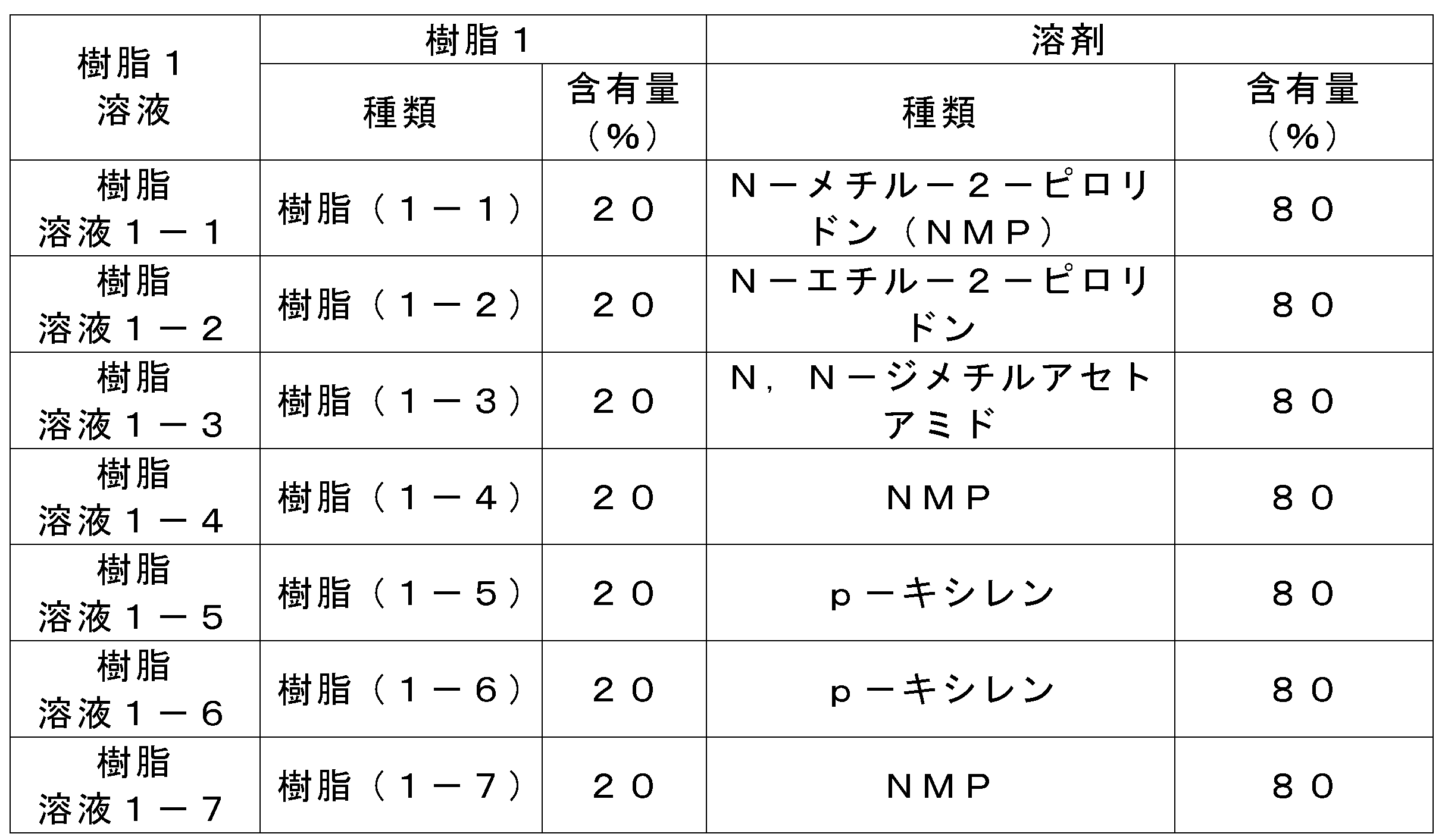
樹脂(1-2):UltrasonE6020(BASF社製、ポリエーテルスルホン樹脂、軟化点240℃、SP値>25)
樹脂(1-3):MRS0810H(佐藤ライト工業製、ポリベンズイミダゾール樹脂、軟化点430℃、SP値>25)
樹脂(1-4):リカコート(新日本理科製、溶剤溶解型ポリイミド樹脂、軟化点320℃、SP値>25)
樹脂(1-5):ザイロンS201A(旭化成製,ポリフェニレンエーテル樹脂、軟化点220℃、SP値20)
樹脂(1-6):ポリスチレン Mw=280,000(アルドリッチ(株)製、ポリスチレン樹脂、軟化点120℃、SP値20)
樹脂(1-7):マラニールナイロン66 A125J (ユニチカ製,ポリアミド樹脂,軟化点 220℃,SP値 >28)
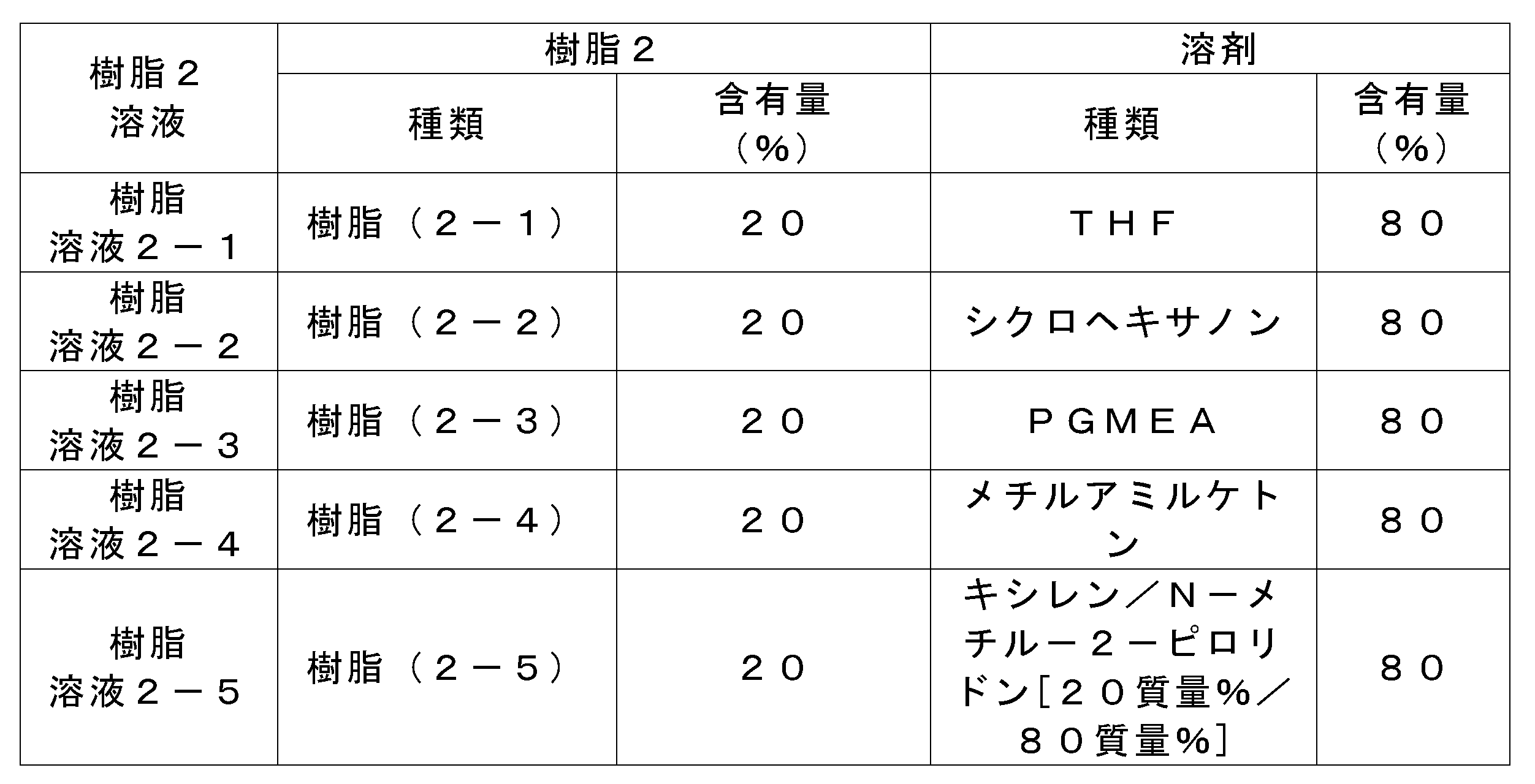
樹脂(2-2):パンライトL-1225LM(帝人製、ポリカーボネート樹脂、SP値22)
樹脂(2-3):エスチレン MS200NT(新日鐵化学製MS樹脂、SP値18)
樹脂(2-4):L-70(ダイセル製、酢酸セルロース樹脂、SP値21)
樹脂(2-5):バイロマックスHR-13NX(東洋紡製、ポリアミドイミド樹脂:ベークにより溶剤不溶化、SP値>25)
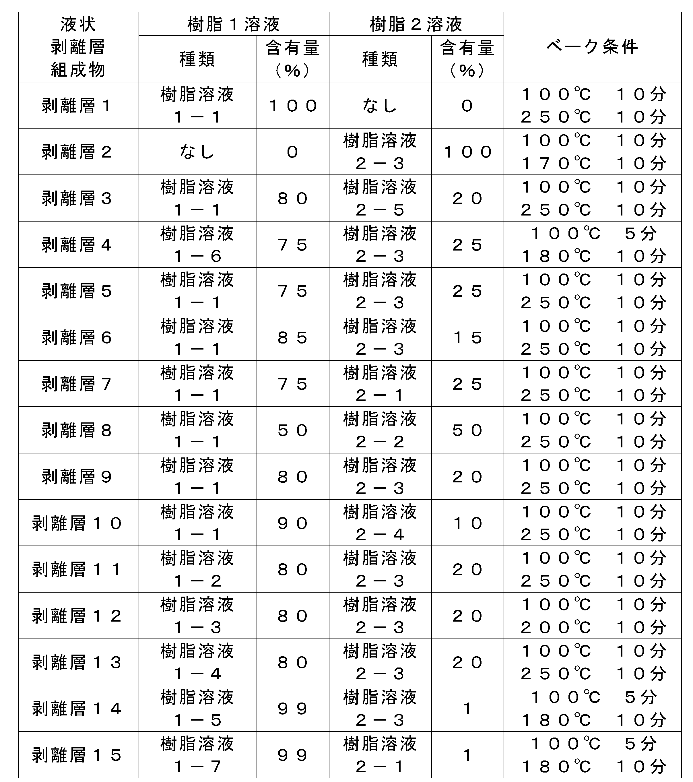
下記表5または6に記載の組み合わせでウエハ1とウエハ2を熱圧着することで試験片を作成した。
表面に何も塗布していない4インチSiウエハまたは剥離層付き4インチSiウエハ(以降ウエハ2とする)を分割し、20mm×30mmのサンプル片とした。同様に分割した20mm×30mmのウエハ1のサンプル片を、その接着性層が、表面に何も塗布していないウエハまたはウエハ2の剥離層に対して20mm×20mmの正方形で接触するように重ね、1N/cm2で120℃、3分間加熱圧着した。
作製された試験片のせん断接着力を、引っ張り試験機(IMADA製)を用いて、250mm/minの条件で接着性層の面に沿った方向に引っ張り測定した。結果を下記表5または6に示す。
作成されたサンプル片を、250mm/minの条件で接着性層の面に垂直な方向に引っ張り測定した(剥離力の測定)。また、作成されたサンプルを表5または6に記載の温度で30分加熱したのち、250mm/minの条件で接着性層の面に垂直な方向に引っ張り測定した(プロセスの最高到達温度下に置かれたことを想定した、耐熱剥離力の測定)。結果を下記表5または6に示す。
作成されたサンプル片を剥離した後、ウエハ2を表5または6記載の溶剤に浸漬させ、ウエハ2から接着性層・剥離層がともに除去されるまでの時間を測定した。結果を表5または6に示す。
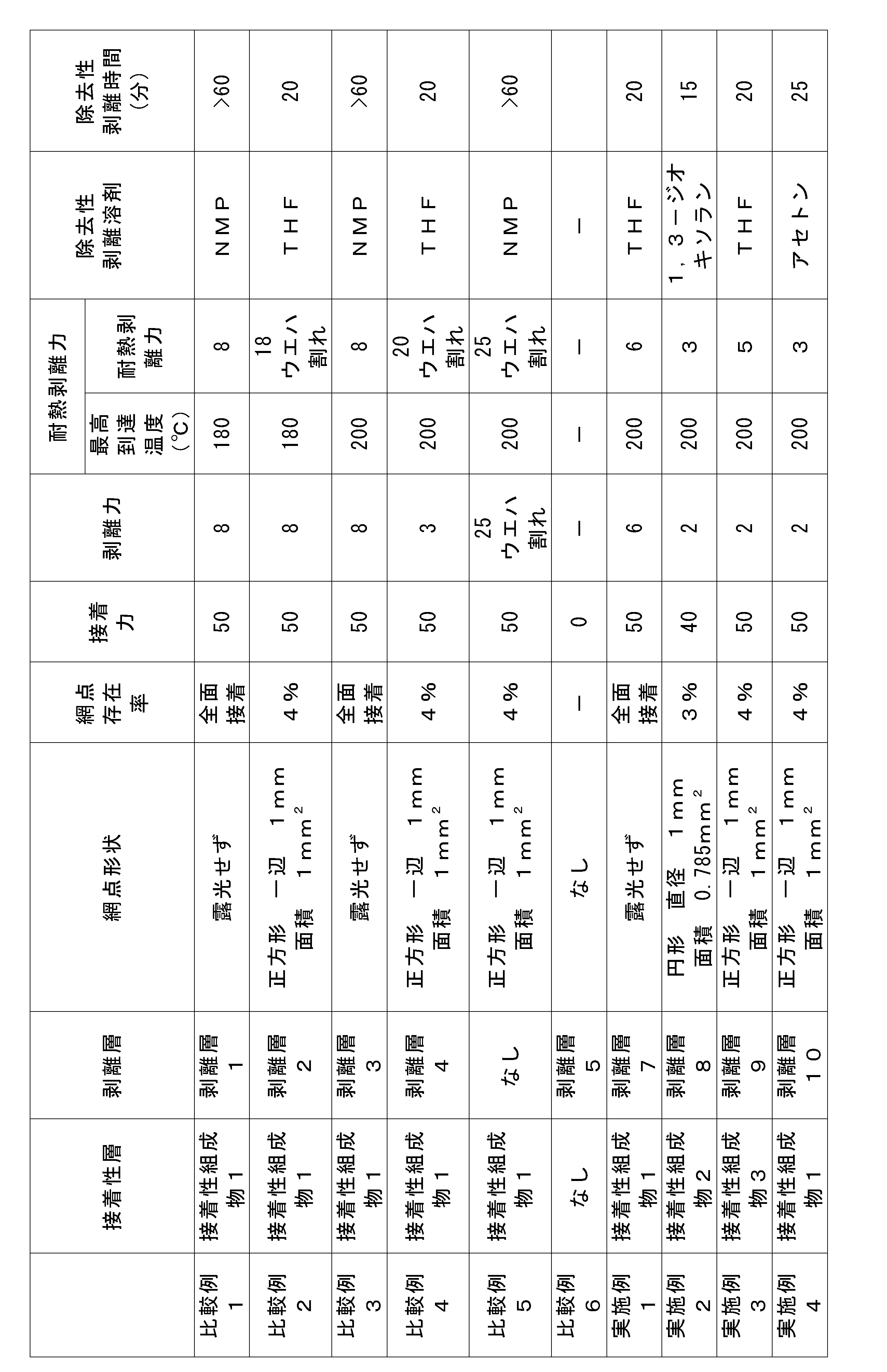
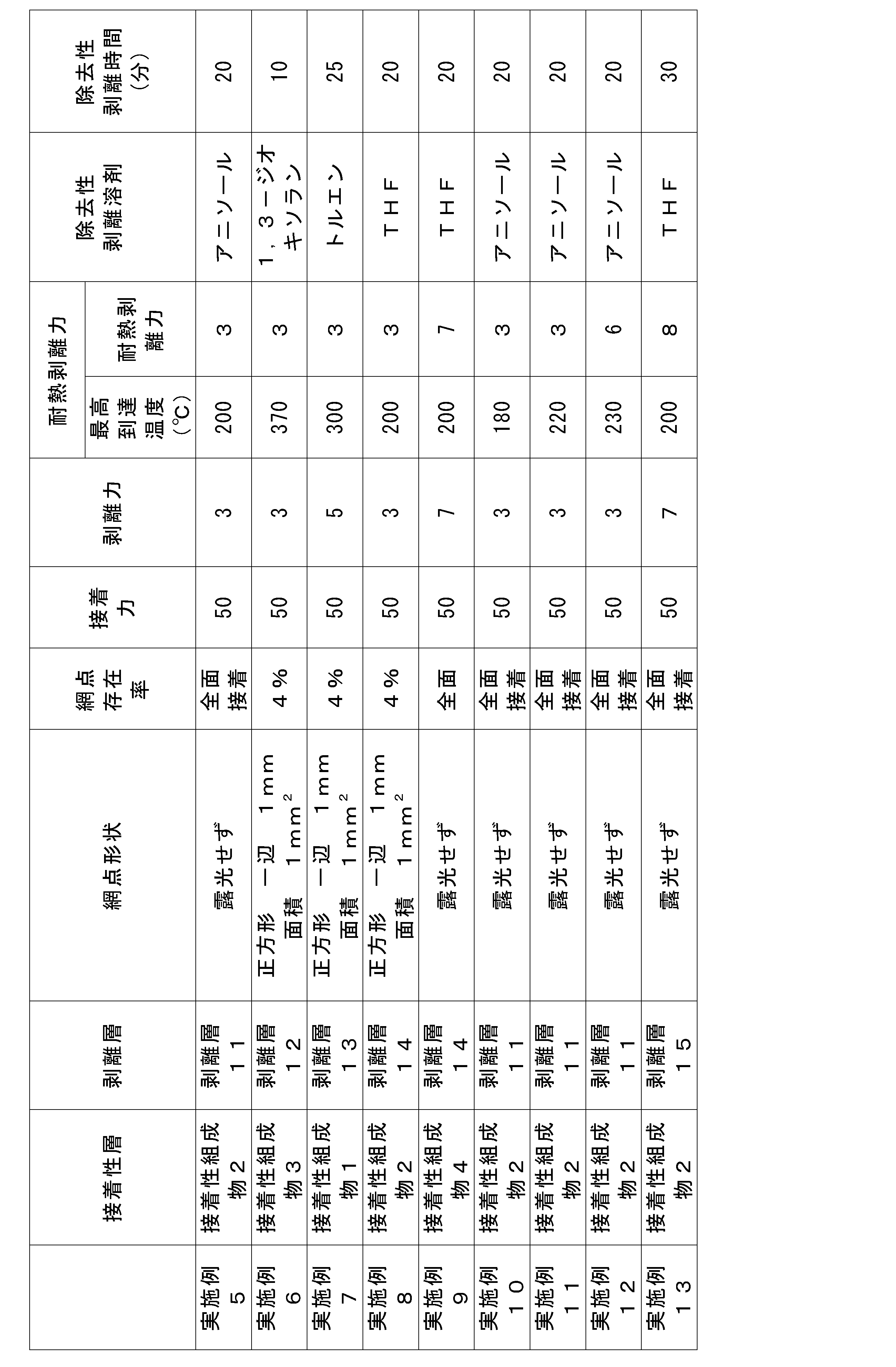
11,21~30,11’ 接着性層
11A、21A~30A 高接着性領域
11B、21B~30B 低接着性領域
12 キャリア基板
60 デバイスウエハ
60’ 薄型デバイスウエハ
61, シリコン基板
61a シリコン基板の表面
61b シリコン基板の裏面
61b’ 薄型デバイスウエハの裏面
62 デバイスチップ
63 バンプ
70 テープ
1,71 剥離層
80 仮接合積層体
100,100’ 接着性支持体
Claims (12)
- (A)剥離層と、(B)接着性層とを有する半導体装置製造用仮接合積層体であって、前記(A)剥離層が、(a1)200℃以上の軟化点を有する樹脂1と、(a2)硬化後に、ヘキサン、ヘプタン、酢酸エチル、アセトン、メタノール、エタノール、イソプロパノール、1,4-ジオキサン、テトラヒドロフラン、1-メトキシ-2-プロパノール、2-アセトキシ-1-メトキシプロパン、アセトニトリル、メチルエチルケトン、シクロヘキサノン、トルエン、ジメチルスルホキシド、N,N-ジメチルホルムアミド、N,N-ジメチルアセトアミド、N-メチル-2-ピロリジノン、N-エチル-2-ピロリジノン、クロロホルム、塩化メチレン、アニソール、キシレン、およびメシチレンから選択される溶剤の少なくとも1種に25℃で5質量%以上溶解する樹脂2を含む、半導体装置製造用仮接合用積層体。
- 前記樹脂1の軟化点が200℃~450℃の範囲内である請求項1に記載の半導体装置製造用仮接合用積層体。
- 前記樹脂1が熱可塑性樹脂である、請求項1または2に記載の半導体装置製造用仮接合用積層体。
- 前記熱可塑性樹脂が、ポリエーテルスルホン樹脂、ポリイミド樹脂、ポリエステル樹脂、ポリベンズイミダゾール樹脂、ポリフェニレンエーテル樹脂、ポリフェニレンスルフィド樹脂およびポリエーテルケトン樹脂から選ばれる少なくとも一種の熱可塑性樹脂である請求項3に記載の半導体装置製造用仮接合用積層体。
- 前記樹脂2が、ポリカーボネート樹脂、ポリウレタン樹脂および炭化水素系樹脂から選ばれる熱可塑性樹脂を含有する、請求項1~4のいずれか1項に記載の半導体装置製造用仮接合用積層体。
- 前記樹脂1と樹脂2とのSP値[MPa1/2]の差が1以上10未満である、請求項1~5のいずれか1項に記載の半導体装置製造用仮接合用積層体。
- 前記(B)接着性層が、バインダーと、重合性モノマーと、光重合開始剤および熱重合開始剤の少なくとも一方とを含む、請求項1~6のいずれか1項に記載の半導体装置製造用仮接合用積層体。
- 被処理部材の第1の面と基板とを、請求項1~7のいずれか1項に記載の半導体装置製造用仮接合用積層体を介在するように接着させる工程、前記被処理部材に対して、180℃~370℃の範囲に最高到達温度を有する加熱処理を施し、処理済部材を得る工程、および、前記仮接合用積層体から前記処理済部材を脱離する工程を有する、前記処理済部材を有する半導体装置の製造方法であって、前記樹脂1の軟化点が、前記加熱処理での最高到達温度より高いことを特徴とする、半導体装置の製造方法。
- 前記被処理部材の第1の面と前記基板とを前記仮接合用積層体を介して接着させる工程の前に、前記仮接合用積層体の接着性層に対して、活性光線若しくは放射線または熱を照射する工程をさらに有する、請求項8に記載の半導体装置の製造方法。
- 前記仮接合用積層体から前記被処理部材を脱離する工程の後、前記被処理部材に残存する前記仮接合用積層体を剥離溶剤により除去する工程をさらに有する、請求項8または9に記載の半導体装置の製造方法。
- 前記剥離溶剤が、炭化水素系溶剤およびエーテル溶剤の少なくとも1種を含む、請求項10に記載の半導体装置の製造方法。
- 前記剥離溶剤が、シクロペンタン、n-ヘキサン、シクロヘキサン、n-ヘプタン、リモネン、p-メンタン、テトラヒドロフラン(THF)、1,3-ジオキソラン、アニソールの少なくとも1種を含む、請求項11に記載の半導体装置の製造方法。
Priority Applications (3)
| Application Number | Priority Date | Filing Date | Title |
|---|---|---|---|
| CN201480018479.XA CN105103267B (zh) | 2013-03-27 | 2014-03-27 | 半导体装置制造用临时粘合用层叠体、和半导体装置的制造方法 |
| KR1020157026284A KR101713090B1 (ko) | 2013-03-27 | 2014-03-27 | 반도체 장치 제조용 가접합용 적층체 및 반도체 장치의 제조방법 |
| US14/865,353 US9716024B2 (en) | 2013-03-27 | 2015-09-25 | Temporary bonding laminates for used in manufacture of semiconductor devices |
Applications Claiming Priority (2)
| Application Number | Priority Date | Filing Date | Title |
|---|---|---|---|
| JP2013066656A JP6050170B2 (ja) | 2013-03-27 | 2013-03-27 | 半導体装置製造用仮接合用積層体、および、半導体装置の製造方法 |
| JP2013-066656 | 2013-03-27 |
Related Child Applications (1)
| Application Number | Title | Priority Date | Filing Date |
|---|---|---|---|
| US14/865,353 Continuation US9716024B2 (en) | 2013-03-27 | 2015-09-25 | Temporary bonding laminates for used in manufacture of semiconductor devices |
Publications (1)
| Publication Number | Publication Date |
|---|---|
| WO2014157440A1 true WO2014157440A1 (ja) | 2014-10-02 |
Family
ID=51624402
Family Applications (1)
| Application Number | Title | Priority Date | Filing Date |
|---|---|---|---|
| PCT/JP2014/058723 Ceased WO2014157440A1 (ja) | 2013-03-27 | 2014-03-27 | 半導体装置製造用仮接合用積層体、および、半導体装置の製造方法 |
Country Status (6)
| Country | Link |
|---|---|
| US (1) | US9716024B2 (ja) |
| JP (1) | JP6050170B2 (ja) |
| KR (1) | KR101713090B1 (ja) |
| CN (1) | CN105103267B (ja) |
| TW (1) | TWI613077B (ja) |
| WO (1) | WO2014157440A1 (ja) |
Cited By (1)
| Publication number | Priority date | Publication date | Assignee | Title |
|---|---|---|---|---|
| CN106783527A (zh) * | 2015-11-23 | 2017-05-31 | 东莞新科技术研究开发有限公司 | 半导体晶片的清洗方法 |
Families Citing this family (14)
| Publication number | Priority date | Publication date | Assignee | Title |
|---|---|---|---|---|
| JP6842878B2 (ja) * | 2016-10-20 | 2021-03-17 | 東京応化工業株式会社 | 接着剤組成物、及びその利用 |
| CN110072685B (zh) * | 2016-12-12 | 2022-05-27 | 东洋纺株式会社 | 热收缩性聚酯系标签、包装体和热收缩性聚酯系标签的制造方法 |
| WO2019106846A1 (ja) * | 2017-12-01 | 2019-06-06 | 日立化成株式会社 | 半導体装置の製造方法、仮固定材用樹脂組成物、及び仮固定材用積層フィルム |
| TWI686461B (zh) * | 2019-02-01 | 2020-03-01 | 才將科技股份有限公司 | 一種具有高矽/二氧化矽蝕刻的選擇比的矽蝕刻劑及其應用 |
| TWI836077B (zh) | 2019-05-22 | 2024-03-21 | 日商力森諾科股份有限公司 | 半導體裝置的製造方法 |
| WO2021131395A1 (ja) * | 2019-12-27 | 2021-07-01 | 東京応化工業株式会社 | 接着剤組成物、積層体、積層体の製造方法、及び電子部品の製造方法 |
| CN111244229B (zh) * | 2020-02-11 | 2021-07-06 | 信利半导体有限公司 | 一种可挠曲的透明薄膜太阳能电池制作方法 |
| WO2021241459A1 (ja) * | 2020-05-26 | 2021-12-02 | 昭和電工マテリアルズ株式会社 | 仮固定用積層フィルム及びその製造方法、仮固定用積層体、並びに半導体装置の製造方法 |
| CN114316872B (zh) * | 2020-09-29 | 2023-09-05 | 上海飞凯材料科技股份有限公司 | 一种临时粘合剂及其应用和应用方法 |
| EP4011996A1 (en) * | 2020-12-11 | 2022-06-15 | Henkel AG & Co. KGaA | Method for detaching adhesively bonded substrates |
| US11996384B2 (en) | 2020-12-15 | 2024-05-28 | Pulseforge, Inc. | Method and apparatus for debonding temporarily bonded wafers in wafer-level packaging applications |
| WO2023065208A1 (zh) * | 2021-10-21 | 2023-04-27 | 3M创新有限公司 | 用于新能源汽车动力电池的封装片材、新能源汽车动力电池组装体及其拆解方法 |
| JP2024545807A (ja) * | 2021-11-11 | 2024-12-12 | ディディピー スペシャルティ エレクトロニック マテリアルズ ユーエス,エルエルシー | 接着剤系 |
| CN115651564B (zh) * | 2022-12-28 | 2023-03-17 | 海阳市凌晖包装有限公司 | 一种激光切割保护膜专用压敏胶及其制备方法 |
Citations (4)
| Publication number | Priority date | Publication date | Assignee | Title |
|---|---|---|---|---|
| WO2009145083A1 (ja) * | 2008-05-28 | 2009-12-03 | 株式会社クレハ | ポリフェニレンサルファイド樹脂製離型フィルム及び積層体 |
| JP2011252094A (ja) * | 2010-06-02 | 2011-12-15 | Sekisui Chem Co Ltd | 離型フィルム |
| WO2012118700A1 (en) * | 2011-02-28 | 2012-09-07 | Dow Corning Corporation | Wafer bonding system and method for bonding and debonding thereof |
| JP2014072451A (ja) * | 2012-09-28 | 2014-04-21 | Fujifilm Corp | 半導体装置製造用仮接合層、積層体、及び、半導体装置の製造方法。 |
Family Cites Families (16)
| Publication number | Priority date | Publication date | Assignee | Title |
|---|---|---|---|---|
| JP2007045939A (ja) | 2005-08-10 | 2007-02-22 | Jsr Corp | 粘着フィルムの粘着力低減方法 |
| WO2007099146A1 (de) | 2006-03-01 | 2007-09-07 | Jakob + Richter Ip-Verwertungsgesellschaft Mbh | Verfahren zum bearbeiten insbesondere dünnen der rückseite eines wafers, wafer-träger-anordnung hierfür und verfahren zur herstellung einer solchen wafer-träger-anordnung |
| US20080014532A1 (en) * | 2006-07-14 | 2008-01-17 | 3M Innovative Properties Company | Laminate body, and method for manufacturing thin substrate using the laminate body |
| US20080200011A1 (en) | 2006-10-06 | 2008-08-21 | Pillalamarri Sunil K | High-temperature, spin-on, bonding compositions for temporary wafer bonding using sliding approach |
| WO2009094558A2 (en) | 2008-01-24 | 2009-07-30 | Brewer Science Inc. | Method for reversibly mounting a device wafer to a carrier substrate |
| JP2010278358A (ja) * | 2009-05-29 | 2010-12-09 | Nitto Denko Corp | フレームレス太陽電池モジュール端部用粘着シール材、フレームレス太陽電池モジュールおよびその端部のシール構造 |
| JP5489546B2 (ja) * | 2009-06-11 | 2014-05-14 | 東京応化工業株式会社 | 貼付方法及び貼付装置 |
| TWI479259B (zh) | 2009-06-15 | 2015-04-01 | 住友電木股份有限公司 | A temporary fixing agent for a semiconductor wafer, and a method of manufacturing the semiconductor device using the same |
| JP2011052142A (ja) | 2009-09-03 | 2011-03-17 | Jsr Corp | 接着剤組成物、それを用いた基材の加工または移動方法および半導体素子 |
| WO2011030716A1 (ja) * | 2009-09-08 | 2011-03-17 | 旭硝子株式会社 | ガラス/樹脂積層体、及びそれを用いた電子デバイス |
| JP5010668B2 (ja) | 2009-12-03 | 2012-08-29 | 信越化学工業株式会社 | 積層型半導体集積装置の製造方法 |
| JP5540814B2 (ja) * | 2010-03-26 | 2014-07-02 | 大日本印刷株式会社 | 粘接着シート |
| JP5691538B2 (ja) | 2010-04-02 | 2015-04-01 | Jsr株式会社 | 仮固定用組成物、仮固定材、基材の処理方法、および半導体素子 |
| JP5523922B2 (ja) * | 2010-04-27 | 2014-06-18 | 東京応化工業株式会社 | 剥離方法及び剥離装置 |
| JP5620782B2 (ja) * | 2010-10-18 | 2014-11-05 | 東京応化工業株式会社 | 積層体及び接着方法 |
| CN106068551B (zh) * | 2014-01-07 | 2019-12-17 | 布鲁尔科技公司 | 用于暂时性晶片粘结方法的环状烯烃聚合物组合物和聚硅氧烷剥离层 |
-
2013
- 2013-03-27 JP JP2013066656A patent/JP6050170B2/ja not_active Expired - Fee Related
-
2014
- 2014-03-19 TW TW103110223A patent/TWI613077B/zh not_active IP Right Cessation
- 2014-03-27 CN CN201480018479.XA patent/CN105103267B/zh not_active Expired - Fee Related
- 2014-03-27 WO PCT/JP2014/058723 patent/WO2014157440A1/ja not_active Ceased
- 2014-03-27 KR KR1020157026284A patent/KR101713090B1/ko not_active Expired - Fee Related
-
2015
- 2015-09-25 US US14/865,353 patent/US9716024B2/en not_active Expired - Fee Related
Patent Citations (4)
| Publication number | Priority date | Publication date | Assignee | Title |
|---|---|---|---|---|
| WO2009145083A1 (ja) * | 2008-05-28 | 2009-12-03 | 株式会社クレハ | ポリフェニレンサルファイド樹脂製離型フィルム及び積層体 |
| JP2011252094A (ja) * | 2010-06-02 | 2011-12-15 | Sekisui Chem Co Ltd | 離型フィルム |
| WO2012118700A1 (en) * | 2011-02-28 | 2012-09-07 | Dow Corning Corporation | Wafer bonding system and method for bonding and debonding thereof |
| JP2014072451A (ja) * | 2012-09-28 | 2014-04-21 | Fujifilm Corp | 半導体装置製造用仮接合層、積層体、及び、半導体装置の製造方法。 |
Cited By (1)
| Publication number | Priority date | Publication date | Assignee | Title |
|---|---|---|---|---|
| CN106783527A (zh) * | 2015-11-23 | 2017-05-31 | 东莞新科技术研究开发有限公司 | 半导体晶片的清洗方法 |
Also Published As
| Publication number | Publication date |
|---|---|
| CN105103267B (zh) | 2017-09-19 |
| JP6050170B2 (ja) | 2016-12-21 |
| TWI613077B (zh) | 2018-02-01 |
| CN105103267A (zh) | 2015-11-25 |
| KR101713090B1 (ko) | 2017-03-07 |
| KR20150125686A (ko) | 2015-11-09 |
| TW201441034A (zh) | 2014-11-01 |
| US9716024B2 (en) | 2017-07-25 |
| US20160104635A1 (en) | 2016-04-14 |
| JP2014192350A (ja) | 2014-10-06 |
Similar Documents
| Publication | Publication Date | Title |
|---|---|---|
| JP6050170B2 (ja) | 半導体装置製造用仮接合用積層体、および、半導体装置の製造方法 | |
| JP5975918B2 (ja) | 半導体装置製造用仮接合用積層体、および、半導体装置の製造方法 | |
| JP6140441B2 (ja) | 半導体装置製造用仮接着剤、並びに、それを用いた接着性支持体、及び、半導体装置の製造方法 | |
| JP6014455B2 (ja) | 半導体装置の製造方法 | |
| JP2014130853A (ja) | 半導体装置製造用仮接着剤、並びに、それを用いた接着性支持体、及び、半導体装置の製造方法 | |
| US9966295B2 (en) | Temporary bonding laminates for use in manufacture of semiconductor devices and method for manufacturing semiconductor devices | |
| JP6068279B2 (ja) | 半導体装置製造用仮接合層、積層体、及び、半導体装置の製造方法 | |
| JP6031264B2 (ja) | 半導体装置製造用仮接着剤、並びに、それを用いた接着性支持体、及び、半導体装置の製造方法 | |
| JP5982248B2 (ja) | 半導体装置製造用仮接合層、積層体、及び、半導体装置の製造方法。 |
Legal Events
| Date | Code | Title | Description |
|---|---|---|---|
| WWE | Wipo information: entry into national phase |
Ref document number: 201480018479.X Country of ref document: CN |
|
| 121 | Ep: the epo has been informed by wipo that ep was designated in this application |
Ref document number: 14774609 Country of ref document: EP Kind code of ref document: A1 |
|
| ENP | Entry into the national phase |
Ref document number: 20157026284 Country of ref document: KR Kind code of ref document: A |
|
| NENP | Non-entry into the national phase |
Ref country code: DE |
|
| 122 | Ep: pct application non-entry in european phase |
Ref document number: 14774609 Country of ref document: EP Kind code of ref document: A1 |