WO2014156161A1 - 金属部品の製造方法並びにそれに用いられる鋳型および離型膜 - Google Patents
金属部品の製造方法並びにそれに用いられる鋳型および離型膜 Download PDFInfo
- Publication number
- WO2014156161A1 WO2014156161A1 PCT/JP2014/001766 JP2014001766W WO2014156161A1 WO 2014156161 A1 WO2014156161 A1 WO 2014156161A1 JP 2014001766 W JP2014001766 W JP 2014001766W WO 2014156161 A1 WO2014156161 A1 WO 2014156161A1
- Authority
- WO
- WIPO (PCT)
- Prior art keywords
- release film
- group
- mold
- film
- atom
- Prior art date
- Legal status (The legal status is an assumption and is not a legal conclusion. Google has not performed a legal analysis and makes no representation as to the accuracy of the status listed.)
- Ceased
Links
Images

Classifications
-
- C—CHEMISTRY; METALLURGY
- C25—ELECTROLYTIC OR ELECTROPHORETIC PROCESSES; APPARATUS THEREFOR
- C25D—PROCESSES FOR THE ELECTROLYTIC OR ELECTROPHORETIC PRODUCTION OF COATINGS; ELECTROFORMING; APPARATUS THEREFOR
- C25D1/00—Electroforming
- C25D1/20—Separation of the formed objects from the electrodes with no destruction of said electrodes
- C25D1/22—Separating compounds
-
- B—PERFORMING OPERATIONS; TRANSPORTING
- B29—WORKING OF PLASTICS; WORKING OF SUBSTANCES IN A PLASTIC STATE IN GENERAL
- B29C—SHAPING OR JOINING OF PLASTICS; SHAPING OF MATERIAL IN A PLASTIC STATE, NOT OTHERWISE PROVIDED FOR; AFTER-TREATMENT OF THE SHAPED PRODUCTS, e.g. REPAIRING
- B29C33/00—Moulds or cores; Details thereof or accessories therefor
- B29C33/56—Coatings, e.g. enameled or galvanised; Releasing, lubricating or separating agents
- B29C33/60—Releasing, lubricating or separating agents
- B29C33/62—Releasing, lubricating or separating agents based on polymers or oligomers
- B29C33/64—Silicone
-
- B—PERFORMING OPERATIONS; TRANSPORTING
- B29—WORKING OF PLASTICS; WORKING OF SUBSTANCES IN A PLASTIC STATE IN GENERAL
- B29C—SHAPING OR JOINING OF PLASTICS; SHAPING OF MATERIAL IN A PLASTIC STATE, NOT OTHERWISE PROVIDED FOR; AFTER-TREATMENT OF THE SHAPED PRODUCTS, e.g. REPAIRING
- B29C33/00—Moulds or cores; Details thereof or accessories therefor
- B29C33/56—Coatings, e.g. enameled or galvanised; Releasing, lubricating or separating agents
- B29C33/68—Release sheets
-
- C—CHEMISTRY; METALLURGY
- C23—COATING METALLIC MATERIAL; COATING MATERIAL WITH METALLIC MATERIAL; CHEMICAL SURFACE TREATMENT; DIFFUSION TREATMENT OF METALLIC MATERIAL; COATING BY VACUUM EVAPORATION, BY SPUTTERING, BY ION IMPLANTATION OR BY CHEMICAL VAPOUR DEPOSITION, IN GENERAL; INHIBITING CORROSION OF METALLIC MATERIAL OR INCRUSTATION IN GENERAL
- C23C—COATING METALLIC MATERIAL; COATING MATERIAL WITH METALLIC MATERIAL; SURFACE TREATMENT OF METALLIC MATERIAL BY DIFFUSION INTO THE SURFACE, BY CHEMICAL CONVERSION OR SUBSTITUTION; COATING BY VACUUM EVAPORATION, BY SPUTTERING, BY ION IMPLANTATION OR BY CHEMICAL VAPOUR DEPOSITION, IN GENERAL
- C23C18/00—Chemical coating by decomposition of either liquid compounds or solutions of the coating forming compounds, without leaving reaction products of surface material in the coating; Contact plating
- C23C18/16—Chemical coating by decomposition of either liquid compounds or solutions of the coating forming compounds, without leaving reaction products of surface material in the coating; Contact plating by reduction or substitution, e.g. electroless plating
- C23C18/1601—Process or apparatus
- C23C18/1633—Process of electroless plating
- C23C18/1646—Characteristics of the product obtained
- C23C18/165—Multilayered product
- C23C18/1653—Two or more layers with at least one layer obtained by electroless plating and one layer obtained by electroplating
-
- C—CHEMISTRY; METALLURGY
- C25—ELECTROLYTIC OR ELECTROPHORETIC PROCESSES; APPARATUS THEREFOR
- C25D—PROCESSES FOR THE ELECTROLYTIC OR ELECTROPHORETIC PRODUCTION OF COATINGS; ELECTROFORMING; APPARATUS THEREFOR
- C25D1/00—Electroforming
- C25D1/10—Moulds; Masks; Masterforms
-
- B—PERFORMING OPERATIONS; TRANSPORTING
- B29—WORKING OF PLASTICS; WORKING OF SUBSTANCES IN A PLASTIC STATE IN GENERAL
- B29C—SHAPING OR JOINING OF PLASTICS; SHAPING OF MATERIAL IN A PLASTIC STATE, NOT OTHERWISE PROVIDED FOR; AFTER-TREATMENT OF THE SHAPED PRODUCTS, e.g. REPAIRING
- B29C33/00—Moulds or cores; Details thereof or accessories therefor
- B29C33/42—Moulds or cores; Details thereof or accessories therefor characterised by the shape of the moulding surface, e.g. ribs or grooves
- B29C33/424—Moulding surfaces provided with means for marking or patterning
-
- B—PERFORMING OPERATIONS; TRANSPORTING
- B29—WORKING OF PLASTICS; WORKING OF SUBSTANCES IN A PLASTIC STATE IN GENERAL
- B29C—SHAPING OR JOINING OF PLASTICS; SHAPING OF MATERIAL IN A PLASTIC STATE, NOT OTHERWISE PROVIDED FOR; AFTER-TREATMENT OF THE SHAPED PRODUCTS, e.g. REPAIRING
- B29C37/00—Component parts, details, accessories or auxiliary operations, not covered by group B29C33/00 or B29C35/00
- B29C37/0067—Using separating agents during or after moulding; Applying separating agents on preforms or articles, e.g. to prevent sticking to each other
- B29C37/0075—Using separating agents during or after moulding; Applying separating agents on preforms or articles, e.g. to prevent sticking to each other using release sheets
Definitions
- the present invention relates to a metal part manufacturing method using an electroforming method, and a mold and a release film used therefor.
- a method for producing a metal part for example, a mold
- a method for producing a metal part for example, a mold
- a metal material is deposited on a pattern surface of a mold by electroforming using a metal mold, and the metal material is peeled off from the mold.
- a release film is formed on the pattern surface before the metal material is deposited by electroforming in order to facilitate the peeling of the metal material from the mold.
- an inorganic release film such as a metal or an inorganic oxide has been conventionally used.
- organic release films have also been used with pattern miniaturization.
- a release film composed of a silane coupling agent having a functional group such as an amino group is used, and an electroless plating is performed using a catalyst applied to the release film.
- a method of forming a current-carrying film and depositing a metal material on the pattern surface by electroforming using the current-carrying film has the advantage that a separate process for forming a current-carrying film by a physical deposition method (for example, a vacuum film-forming method or the like) is unnecessary, and the manufacturing process of metal parts is simplified as a whole.
- the present invention has been made in view of the above problems, and provides a metal part manufacturing method and a mold and a release film used for the metal part that make it possible to easily release the metal part in the manufacture of the metal part. It is intended to do.
- a method for manufacturing a metal part according to the present invention includes: Forming a release film containing a compound represented by the following general formula on the uneven pattern surface of the mold body, Adding a catalyst for electroless plating to the release film, An electroforming film for electroforming is formed on the release film by electroless plating using a catalyst, The metal material is deposited on the conductive film by electroforming using the conductive film, The deposited metal material is peeled off from the mold body.
- the mold according to the present invention is A mold used in a method of manufacturing a metal part, A mold body having an uneven pattern surface on the surface; And a release film containing a compound represented by the following general formula formed on the concavo-convex pattern surface.
- the release film according to the present invention is A mold release film formed on a concavo-convex pattern surface of a mold main body used in a method for producing a metal part, comprising a compound represented by the following general formula.
- X is a group containing an aromatic ring
- L is a linking group having 1 to 10 carbon atoms containing at least one of a nitrogen atom (N), a sulfur atom (S), and an oxygen atom (O);
- R is a hydrogen atom or an alkyl group having 1 to 4 carbon atoms.
- X preferably contains a phenyl group, a pyridyl group or a thienyl group.
- the compound is preferably a silane coupling agent, and in particular, trimethoxy [3- (phenylamino) propyl] silane, N -Phenylaminomethyltriethoxysilane, 2- (3-trimethoxysilylpropylthio) thiophene, 2-hydroxy-4- (3-triethoxysilylpropoxy) diphenyl ketone and 2- (4-pyridylethyl) thiopropyltri Of the methoxysilane, at least one compound is preferable.
- the material constituting the mold body is preferably any one of metal, glass, inorganic oxide, and resin.
- the method for producing a metal part according to the present invention and the mold and release film used therefor are characterized by using a compound having an aromatic ring.
- the present inventor has found that the release part can easily release the metal part by having an aromatic ring. Therefore, by using a compound having an aromatic ring, the metal part can be released more easily in the production of the metal part.
- the mold manufacturing method of the present embodiment prepares a mold body 20 having a surface with a concavo-convex pattern (a concavo-convex pattern surface) (A in FIG. 1), and is represented by the following general formula.
- a release film 16 composed of a compound is formed on the concavo-convex pattern surface (B in FIG. 1), a catalyst for electroless plating is adsorbed on the release film 16, and then electroless plating using the catalyst is performed.
- An electroforming film 14 for electroforming is formed on the release film 16 (C in FIG. 1), and the metal material 12 is deposited on the electroconductive film 14 by electroforming using the electroconductive film 14 (D in FIG. 1). The deposited metal material 12 is peeled from the mold body 20 (E in FIG. 1).
- X is a group containing an aromatic ring
- L is a linking group having 1 to 10 carbon atoms containing at least one of a nitrogen atom (N), a sulfur atom (S), and an oxygen atom (O);
- R is a hydrogen atom or an alkyl group having 1 to 4 carbon atoms.
- the mold 10 composed of the metal material 12 and the conductive film 14 is manufactured.
- the mold release film 16 may partially adhere to the mold surface, but such deposits can be removed by a cleaning method such as ozone cleaning.
- the template of the present embodiment is composed of a mold body 20 and a release film 16 composed of the above compound, and the mold release film of this embodiment is a release film composed of the above compound. 16.
- the material constituting the mold body 20 is not particularly limited, and examples thereof include metals such as Ni, Ni—P, Ni—B, Ti and W, inorganic oxides such as silicon oxide, glass such as quartz glass, acrylic resin, and the like. Any of resins such as styrene resin may be used.
- the mold body 20 has a concavo-convex pattern to be transferred to the mold.
- the shape of the convex part or concave part of the concavo-convex pattern is appropriately designed such as a polygonal columnar shape, a polygonal pyramid shape, a columnar shape, a conical shape, a dome shape or the like.
- the width of the projection or recess in plan view is, for example, 10 nm to 10 ⁇ m, and the height or depth is 10 nm to 10 ⁇ m.
- the group containing an aromatic ring represented by X is not particularly limited as long as it contains an aromatic ring (including a heteroaromatic ring).
- an aromatic ring including a heteroaromatic ring.
- a group containing at least one of a phenyl group, a pyridyl group and a thienyl group is particularly preferred.
- the aromatic ring has a monovalent structure (one bond) with respect to the bond to L.
- a phenyl group can have a structure of — (C 6 H 5 ), a pyridyl group can have a structure of — (C 5 H 4 N), and a thienyl group can be a structure of — (C 4 H 3 S).
- the aromatic ring may have a substituent other than the coupling
- the linking group L includes at least one of a nitrogen atom (N), a sulfur atom (S), and an oxygen atom (O).
- N nitrogen atom
- S sulfur atom
- O oxygen atom
- the positions of the nitrogen atom, sulfur atom and oxygen atom are not particularly limited, but these atoms are preferably contained in the main chain of the linking group L in the form of —NH—, —S— and —O—, respectively.
- the compound in the present invention is a so-called silane coupling agent having a structure of —Si— (O—R) 3 .
- R is particularly preferably a methyl group or an ethyl group.
- silane coupling agent having an aromatic ring and —NH— structure examples include 3- (phenylamino) propyltrimethoxysilane and N-phenylaminomethyltriethoxysilane.
- silane coupling agent having an aromatic ring and —S— structure examples include 2- (3-trimethoxysilylpropylthio) thiophene.
- silane coupling agent having both an aromatic ring and —O— structure include 2-hydroxy-4- (3-triethoxysilylpropioxy) diphenyl ketone.
- a known method can be used as a method for forming the release film 16.
- a liquid phase method such as a vapor phase method, a dipping method using a solution containing a compound, a coating method, or a spray method can be used.
- the release film 16 is a monomolecular layer film or a thin film close thereto, and the film thickness is about several to several tens of millimeters.
- Such a release film 16 has extremely high followability to the shape of the concavo-convex pattern surface of the mold body 20.
- a known method can be used as the application of the electroless plating catalyst to the release film 16 and the subsequent formation of the electroforming film for electroforming by electroless plating.
- a method for applying a catalyst known methods such as an immersion method, a coating method, and a spray method using a catalyst applying solution can be used.
- a desired catalyst Pd, Ag, Cu, Ni, etc.
- the catalyst application liquid is appropriately selected according to the material to be deposited by electroless plating (that is, the material of the conductive film 14).
- the release film 16 when the release film 16 contains at least one kind of atom of nitrogen atom, sulfur atom and oxygen atom, the release film 16 has a property of adsorbing metal ions (Pd 2+, etc.) serving as a catalyst. Therefore, the catalyst can be reliably adsorbed on the release film 16. Electroless plating is performed, for example, by immersing a mold provided with a catalyst in a plating tank filled with a plating solution. When the mold is immersed, the plating material is deposited on the release film 16 by catalytic action, and the deposited material forms a film, whereby the conductive film 14 is formed. As described above, according to the present invention, since a large-scale apparatus such as vacuum film formation or a laborious film formation method is not required in the process of forming the energization film, the process becomes simple.
- a large-scale apparatus such as vacuum film formation or a laborious film formation method is not required in the process of forming the energization film, the process becomes simple.
- the thickness of the conductive film 14 is preferably set within a range of 0.05 to 0.5 ⁇ m. If the thickness of the current-carrying film 14 is less than 0.05 ⁇ m, there is a risk of disconnection during electroforming, and if it exceeds 0.5 ⁇ m, the internal stress of the current-carrying film 14 increases and the current-carrying film 14 becomes the mold body. This is because there is a possibility of peeling off from 20.
- Electroforming is performed by immersing a mold in which the conductive film 14 is formed in an electroforming solution, and energizing the conductive film 14 to deposit a metal material on the conductive film 14.
- electroforming conditions such as the type of electroforming liquid used to deposit the metal material, the liquid temperature and pH, the current density, and the energization time.
- an electroforming solution can be appropriately selected from known materials, and conditions can be set as appropriate according to the mold to be manufactured.
- the metal material include Ni, Cr, Cu, Ni—Cr alloy, Ni—Fe alloy, and Ni—W alloy.
- the final thickness of the deposited metal material is preferably 10 ⁇ m or more. This is because if the thickness is less than 10 ⁇ m, the mold may be damaged in the next peeling step.
- the release film 16 since the release film 16 contains an aromatic ring, the release film 16 has good release properties. This is thought to be because the regularity and denseness of the release film molecules are increased by stacking aromatic rings by ⁇ - ⁇ electron interaction. Therefore, the mold 10 having a fine shape of nanometer order can be manufactured with high reproducibility. Moreover, the process of dissolving and removing the release film at the time of peeling is unnecessary, and the manufacturing process becomes simpler.
- the metal material 12 is peeled off, the metal material 12 may be peeled off as a single unit. However, after the reinforcing material is further bonded onto the metal material 12, the metal material 12 may be peeled off together with the reinforcing material. Good. In this case, it is possible to obtain a mold supported on the reinforcing material.
- the mold manufacturing method and the mold according to the present invention use a release film made of a compound having an aromatic ring, the mold can be easily released. Therefore, the mold can be released more easily in the manufacture of the mold.
- the release film of the present invention is composed of a compound having an aromatic ring, it has high releasability.
- Example 1 Surface activation treatment was performed on a 6-inch silicon wafer that had been subjected to nano-scale microfabrication in a 4-inch circular region by anisotropic etching or the like using a UV-O 3 cleaner (manufactured by Sen Special Light Source Co., Ltd.). .
- 3- (phenylamino) propyltrimethoxysilane (manufactured by Tokyo Chemical Industry Co., Ltd.), which is a silane coupling agent, was used as a release agent, and the volume ratio (volume of silane coupling agent / volume of container) was The release agent was sealed in a sealed container together with the silicon wafer wafer so as to be 10 mL / L. This sealed container was placed in an oven and heated at 100 ° C. for 2 hours. Thereafter, the silicon wafer was taken out and the release agent was removed with an appropriate solvent to form a release film.
- the structural formula of 3- (phenylamino) propyltrimethoxysilane is as shown in the following structural formula 1.
- the silicon wafer on which the release film is formed is immersed in a SnCl 2 (Wako Pure Chemical Industries, Ltd.) solution (room temperature) for 1 minute, washed with water, and then further PdCl 2 (Wako Pure Chemical Industries, Ltd.).
- the catalyst was provided by immersing in a solution (room temperature) for 1 minute and washing with water.
- the silicon wafer is immersed in a nickel electroforming solution and energized to the current-carrying film at a current density of 4 A / dm 2 for 150 minutes to deposit nickel. I let you.
- the final thickness of the electroformed coating is 150 ⁇ m.
- Example 2 A mold was produced in the same manner as in Example 1 except that N-phenylaminomethyltriethoxysilane (manufactured by Gelest) was used as a release agent.
- the structural formula of N-phenylaminomethyltriethoxysilane is as shown in the following structural formula 2.
- Example 3 A mold was produced in the same manner as in Example 1 except that 2- (3-trimethoxysilylpropylthio) thiophene (manufactured by Gelest Co.) was used as a release agent.
- the structural formula of 2- (3-trimethoxysilylpropylthio) thiophene is as shown in the following structural formula 3.
- Example 4 A mold was produced in the same manner as in Example 1 except that 2-hydroxy-4- (3-triethoxysilylpropioxy) diphenyl ketone (manufactured by Gelest Co.) was used as a release agent.
- the structural formula of 2-hydroxy-4- (3-triethoxysilylpropoxy) diphenyl ketone is as shown in the following structural formula 4.
- the ring structure on the right side corresponds to the aromatic ring in the present invention.
- Example 5 A mold was produced in the same manner as in Example 1 except that 2- (4-pyridylethyl) thiopropyltrimethoxysilane (manufactured by Gelest) was used as a mold release agent.
- the structural formula of 2- (4-pyridylethyl) thiopropyltrimethoxysilane is as shown in the following structural formula 5.
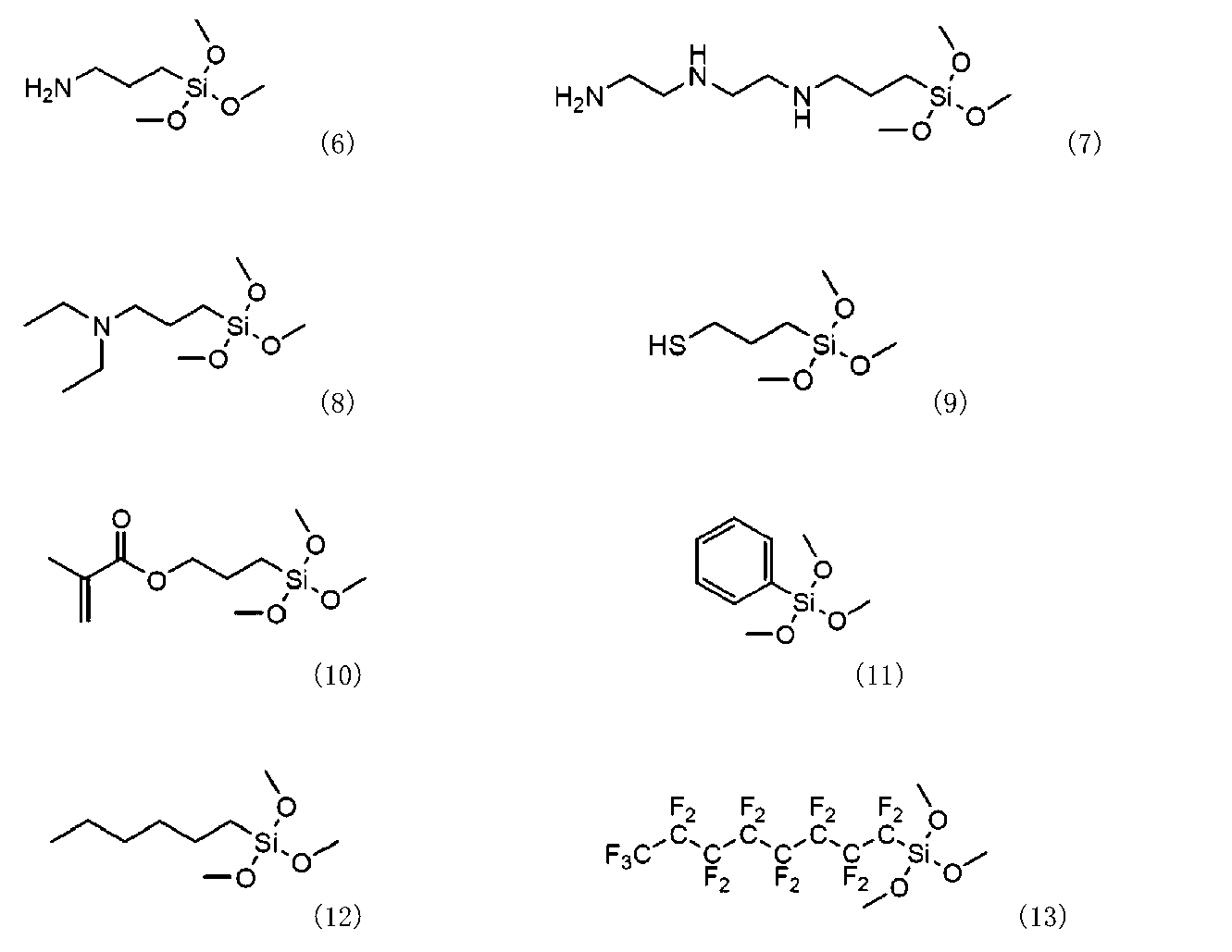
- the structural formulas of the respective compounds are as shown in the following structural formulas 6 to 13, respectively.
- Table 1 summarizes the evaluation results in each example and each comparative example.
- Example 1 to 5 when the release agent is a compound having at least one atom of nitrogen atom, sulfur atom and oxygen atom (Examples 1 to 5 and Comparative Examples 1 to 4 have excellent catalyst adsorption)
- the release agent when the release agent is a compound having both the above atoms and an aromatic ring (Examples 1 to 5), it is possible to form a release film. It was confirmed that the nickel electroformed film can be peeled without deformation as compared with the case where the agent is another eight kinds of compounds (Comparative Examples 1 to 8).
- the release agent is a compound having a nitrogen atom (amino group) or a sulfur atom (thio group) but not an aromatic ring (Comparative Examples 1 to 4)
- the current-carrying film and the silicon wafer are in close contact with each other. It was confirmed that the nickel electroformed film was deformed during peeling.
- the release agent is another compound that cannot be expected to adsorb the catalyst (Comparative Examples 5 to 8)
- the nickel does not precipitate or a part of the current-carrying film that does not precipitate even if it is deposited. Peeling was seen.
- Example 6 As the mold body, an original plate made of nickel that was ultra-fine processed by etching or the like was used. Then, an energization film was formed by the same process as in Example 1 using this original plate. At this time, it was confirmed by visual observation that a flat and uniform conductive film could be formed. Then, the metal mold
- Example 7 As the mold body, an original plate made of silicon oxide (quartz) subjected to ultrafine processing by etching or the like was used. Then, an energization film was formed by the same process as in Example 1 using this original plate. At this time, it was confirmed by visual observation that a flat and uniform conductive film could be formed. Then, the metal mold
- Example 8 As the mold body, an original plate made of an acrylic resin subjected to ultrafine processing by etching or the like was used. And using this original plate, an energization film was formed by the same process as in Example 1. At this time, it was confirmed that a flat and uniform conductive film could be formed visually. Then, the metal mold
- ⁇ Comparative Example 9 First, surface activation treatment is performed on a 6-inch silicon wafer that has been subjected to nano-scale microfabrication in a 4-inch circular region by anisotropic etching or the like using a UV-O 3 cleaner (manufactured by Sen Special Light Source Co., Ltd.). went. Then, a platinum thin film was formed by sputtering as a release film on the finely processed region of the silicon wafer. Then, the electroforming process was performed similarly to Example 1, and the peeling process was tried. However, the nickel electroformed film formed by electroforming could not be peeled off and a mold could not be obtained.
- a UV-O 3 cleaner manufactured by Sen Special Light Source Co., Ltd.
- the metal part manufacturing method of the present invention is applied to the manufacture of a mold.
- what can be manufactured is not limited to a mold, and it is also possible to manufacture metal parts having fine-shaped parts on the order of nanometers such as wiring, electrodes, and imaging devices.
Landscapes
- Chemical & Material Sciences (AREA)
- Engineering & Computer Science (AREA)
- Mechanical Engineering (AREA)
- Chemical Kinetics & Catalysis (AREA)
- Materials Engineering (AREA)
- Metallurgy (AREA)
- Organic Chemistry (AREA)
- Electrochemistry (AREA)
- General Chemical & Material Sciences (AREA)
- Moulds For Moulding Plastics Or The Like (AREA)
- Chemically Coating (AREA)
Abstract
Description
鋳型本体の凹凸パターン面上に下記一般式で表される化合物を含む離型膜を形成し、
離型膜に無電解めっき用の触媒を付与し、
触媒を利用した無電解めっきにより離型膜上に電鋳用の通電膜を形成し、
通電膜を使用した電鋳により通電膜上に金属材を析出させ、
析出した金属材を鋳型本体から剥離することを特徴とするものである。
金属部品の製造方法に用いられる鋳型であって、
表面に凹凸パターン面を有する鋳型本体と、
上記凹凸パターン面上に形成された下記一般式で表される化合物を含む離型膜とを備えることを特徴とするものである。
金属部品の製造方法に用いられる鋳型本体の凹凸パターン面上に形成される離型膜であって、下記一般式で表される化合物を含むことを特徴とするものである。
Xは、芳香環を含む基であり、
Lは、窒素原子(N)、硫黄原子(S)および酸素原子(O)の少なくとも1つを含む炭素数1~10の連結基であり、
Rは、水素原子または炭素数1~4のアルキル基である。
Xは、芳香環を含む基であり、
Lは、窒素原子(N)、硫黄原子(S)および酸素原子(O)の少なくとも1つを含む炭素数1~10の連結基であり、
Rは、水素原子または炭素数1~4のアルキル基である。
異方性エッチング等によりナノスケールの微細加工を4インチ円領域に施した6インチのシリコンウェハに対し、UV-O3クリーナー(セン特殊光源株式会社製)を用いて表面活性化処理を行った。

離型剤としてN-フェニルアミノメチルトリエトキシシラン(Gelest社製)を使用した点以外は、実施例1と同様に金型を製造した。なお、N-フェニルアミノメチルトリエトキシシランの構造式は下記構造式2の通りである。

離型剤として2-(3-トリメトキシシリルプロピルチオ)チオフェン(Gelest社製)を使用した点以外は、実施例1と同様に金型を製造した。なお、2-(3-トリメトキシシリルプロピルチオ)チオフェンの構造式は下記構造式3の通りである。

離型剤として2-ヒドロキシ-4-(3-トリエトキシシリルプロピオキシ)ジフェニルケトン(Gelest社製)を使用した点以外は、実施例1と同様に金型を製造した。なお、2-ヒドロキシ-4-(3-トリエトキシシリルプロピオキシ)ジフェニルケトンの構造式は下記構造式4の通りである。なお構造式4において、右側の環構造が本発明における芳香環に相当する。

離型剤として2-(4-ピリジルエチル)チオプロピルトリメトキシシラン(Gelest社製)を使用した点以外は、実施例1と同様に金型を製造した。なお、2-(4-ピリジルエチル)チオプロピルトリメトキシシランの構造式は下記構造式5の通りである。

また、離型剤として下記に示す化合物をそれぞれ使用して実施例1と同様の工程を試みた。なお、各化合物の構造式はそれぞれ下記構造式6~13の通りである。
比較例1:3-アミノプロピルトリメトキシシラン(構造式6)(東京化成工業株式会社製)
比較例2:N1-(3-トリメトキシプロピル)ジエチレントリアミン(構造式7)(ALDRICH社製)
比較例3:3-(N,N-ジエチルアミノ)プロピルトリメトキシシラン(構造式8)(Fluorochem Ltd.製)
比較例4:3-メルカプトプロピルメチルジメトキシシラン(構造式9)(東京化成工業株式会社製)
比較例5:3-メタクリルオキシプロピルトリメトキシシラン(構造式10)(信越化学工業株式会社製)
比較例6:トリメトキシフェニルシラン(構造式11)(東京化成工業株式会社製)
比較例7:ヘキシルトリメトキシシラン(構造式12)(東京化成工業株式会社製)
比較例8:1H, 1H,2H,2H-ペルフルオロオクチルトリエトキシシラン(構造式13)(ALDRICH社製)
上記の各実施例および各比較例において、無電解ニッケルめっきの析出性およびニッケル電鋳被膜の離型性について評価を行った。各項目の評価基準は下記の通りである。
(無電解ニッケルめっきの析出性)
目視において平坦で均一な通電膜が形成できた場合に「Good」と評価し、ニッケルが析出しないか、析出しても一部析出しない部分や通電膜の剥がれが見られる場合に「Bad」と評価した。
(ニッケル電鋳被膜の離型性)
ニッケル電鋳被膜を離型できかつ目視でニッケル電鋳被膜の変形が確認されなかった場合に「Good」と評価し、ニッケル電鋳被膜を離型できたが目視でニッケル電鋳被膜の変形が確認された場合または離型自体ができなかった場合に「Bad」と評価した。
表1は各実施例および各比較例においての評価結果をまとめたものである。

鋳型本体として、エッチング等により超微細加工を施したニッケルからなる原板を使用した。そして、この原板を使用して実施例1と同様の工程により通電膜を形成した。このとき、目視で平坦で均一な通電膜が形成できたことを確認した。その後、実施例1と同様の工程により金型を得た。この金型は、原板の微細形状を良好に反映した微細形状を有し、目視で変形がないことを確認した。
鋳型本体として、エッチング等により超微細加工を施した酸化珪素(石英)からなる原板を使用した。そして、この原板を使用して実施例1と同様の工程により通電膜を形成した。このとき、目視で平坦で均一な通電膜が形成できたことを確認した。その後、実施例1と同様の工程により金型を得た。この金型は、原板の微細形状を良好に反映した微細形状を有し、目視で変形がないことを確認した。
鋳型本体として、エッチング等により超微細加工を施したアクリル樹脂からなる原板を使用した。そして、この原板を使用して実施例1と同様の工程により通電膜を形成した。このとき、目視で平坦で均一な通電膜が形成できたことを確認した。その後、実施例1と同様の工程により金型を得た。この金型は、原板の微細形状を良好に反映した微細形状を有し、目視で変形がないことを確認した。
まず、異方性エッチング等によりナノスケールの微細加工を4インチ円領域に施した6インチのシリコンウェハに対し、UV-O3クリーナー(セン特殊光源株式会社製)を用いて表面活性化処理を行った。そして、このシリコンウェハの微細加工領域上に離型膜としてスパッタリング法により白金薄膜を形成した。その後、実施例1と同様に電鋳工程を行い、剥離工程を試みた。しかし、電鋳により形成したニッケル電鋳被膜は剥離することができず、金型を得ることはできなかった。
Claims (10)
- 鋳型本体の凹凸パターン面上に下記一般式1で表される化合物を含む離型膜を形成し、
前記離型膜に無電解めっき用の触媒を付与し、
前記触媒を利用した無電解めっきにより前記離型膜上に電鋳用の通電膜を形成し、
前記通電膜を使用した電鋳により前記通電膜上に金属材を析出させ、
析出した前記金属材を前記鋳型本体から剥離することを特徴とする金属部品の製造方法。
X-L-Si―(O-R)3 (1)
式1において、Xは、芳香環を含む基であり、
Lは、窒素原子、硫黄原子および酸素原子の少なくとも1つを含む炭素数1~10の連結基であり、
Rは、水素原子または炭素数1~4のアルキル基である。 - 前記Xがフェニル基、ピリジル基またはチエニル基を含むことを特徴とする請求項1に記載の金属部品の製造方法。
- 前記化合物が、トリメトキシ[3-(フェニルアミノ)プロピル]シラン、N-フェニルアミノメチルトリエトキシシラン、2-(3-トリメトキシシリルプロピルチオ)チオフェン、2-ヒドロキシ-4-(3-トリエトキシシリルプロピオキシ)ジフェニルケトンおよび2-(4-ピリジルエチル)チオプロピルトリメトキシシランのうち少なくとも一種の化合物であることを特徴とする請求項2に記載の金属部品の製造方法。
- 金属部品の製造方法に用いられる鋳型であって、
表面に凹凸パターン面を有する鋳型本体と、
前記凹凸パターン面上に形成された下記一般式2で表される化合物を含む離型膜とを備えることを特徴とする鋳型。
X-L-Si―(O-R)3 (2)
式2において、Xは、芳香環を含む基であり、
Lは、窒素原子、硫黄原子および酸素原子の少なくとも1つを含む炭素数1~10の連結基であり、
Rは、水素原子または炭素数1~4のアルキル基である。 - 前記Xがフェニル基、ピリジル基またはチエニル基を含むことを特徴とする請求項4に記載の鋳型。
- 前記化合物が、トリメトキシ[3-(フェニルアミノ)プロピル]シラン、N-フェニルアミノメチルトリエトキシシラン、2-(3-トリメトキシシリルプロピルチオ)チオフェン、2-ヒドロキシ-4-(3-トリエトキシシリルプロピオキシ)ジフェニルケトンおよび2-(4-ピリジルエチル)チオプロピルトリメトキシシランのうち少なくとも一種の化合物であることを特徴とする請求項5に記載の鋳型。
- 前記鋳型本体を構成する材料が、金属、ガラス、無機酸化物および樹脂のいずれかであることを特徴とする請求項4から6いずれかに記載の鋳型。
- 金属部品の製造方法に用いられる鋳型本体の凹凸パターン面上に形成される離型膜であって、
下記一般式3で表される化合物を含むことを特徴とする離型膜。
X-L-Si―(O-R)3 (3)
式3において、Xは、芳香環を含む基であり、
Lは、窒素原子、硫黄原子および酸素原子の少なくとも1つを含む炭素数1~10の連結基であり、
Rは、水素原子または炭素数1~4のアルキル基である。 - 前記Xがフェニル基、ピリジル基またはチエニル基を含むことを特徴とする請求項8に記載の離型膜。
- 前記化合物が、トリメトキシ[3-(フェニルアミノ)プロピル]シラン、N-フェニルアミノメチルトリエトキシシラン、2-(3-トリメトキシシリルプロピルチオ)チオフェン、2-ヒドロキシ-4-(3-トリエトキシシリルプロピオキシ)ジフェニルケトンおよび2-(4-ピリジルエチル)チオプロピルトリメトキシシランのうち少なくとも一種の化合物であることを特徴とする請求項9に記載の離型膜。
Priority Applications (2)
| Application Number | Priority Date | Filing Date | Title |
|---|---|---|---|
| CN201480017644.XA CN105051259A (zh) | 2013-03-28 | 2014-03-27 | 金属零件的制造方法及用于其的铸模及离型膜 |
| KR1020157029370A KR20150126705A (ko) | 2013-03-28 | 2014-03-27 | 금속 부품의 제조 방법 그리고 그것에 사용되는 주형 및 이형막 |
Applications Claiming Priority (2)
| Application Number | Priority Date | Filing Date | Title |
|---|---|---|---|
| JP2013-068361 | 2013-03-28 | ||
| JP2013068361A JP6066484B2 (ja) | 2013-03-28 | 2013-03-28 | 金属部品の製造方法並びにそれに用いられる鋳型および離型膜 |
Publications (1)
| Publication Number | Publication Date |
|---|---|
| WO2014156161A1 true WO2014156161A1 (ja) | 2014-10-02 |
Family
ID=51623173
Family Applications (1)
| Application Number | Title | Priority Date | Filing Date |
|---|---|---|---|
| PCT/JP2014/001766 Ceased WO2014156161A1 (ja) | 2013-03-28 | 2014-03-27 | 金属部品の製造方法並びにそれに用いられる鋳型および離型膜 |
Country Status (5)
| Country | Link |
|---|---|
| JP (1) | JP6066484B2 (ja) |
| KR (1) | KR20150126705A (ja) |
| CN (1) | CN105051259A (ja) |
| TW (1) | TWI619591B (ja) |
| WO (1) | WO2014156161A1 (ja) |
Cited By (1)
| Publication number | Priority date | Publication date | Assignee | Title |
|---|---|---|---|---|
| WO2016063463A1 (ja) * | 2014-10-21 | 2016-04-28 | 日本曹達株式会社 | 有機薄膜製造方法 |
Families Citing this family (4)
| Publication number | Priority date | Publication date | Assignee | Title |
|---|---|---|---|---|
| CN106430081A (zh) * | 2016-10-14 | 2017-02-22 | 河南理工大学 | 一种圆柱模具的制造方法 |
| JP7731248B2 (ja) * | 2021-09-17 | 2025-08-29 | 富士フイルム株式会社 | 電鋳用原盤、電鋳用原盤の製造方法及び電鋳物の製造方法 |
| JP7779693B2 (ja) * | 2021-09-30 | 2025-12-03 | 富士フイルム株式会社 | 電鋳方法及び電鋳物の製造方法 |
| CN116353188B (zh) * | 2023-03-29 | 2024-07-26 | 上海新倬壮印刷科技有限公司 | 一种丝印网版加工工艺 |
Citations (2)
| Publication number | Priority date | Publication date | Assignee | Title |
|---|---|---|---|---|
| JP2005120392A (ja) * | 2003-10-14 | 2005-05-12 | Meltex Inc | 金属部品の製造方法 |
| WO2006070857A1 (ja) * | 2004-12-28 | 2006-07-06 | Nippon Soda Co., Ltd. | 剥離層を有する成形用金型又は電鋳用母型 |
Family Cites Families (5)
| Publication number | Priority date | Publication date | Assignee | Title |
|---|---|---|---|---|
| US20050023433A1 (en) * | 2003-07-31 | 2005-02-03 | Alps Electric Co., Ltd. | Resin optical component mold having minute concavo-convex portions and method of manufacturing resin optical component using the same |
| JP2007246949A (ja) * | 2006-03-14 | 2007-09-27 | Sony Corp | 導電性パターンの形成方法および電子基板 |
| JP5172534B2 (ja) * | 2008-08-21 | 2013-03-27 | 松本油脂製薬株式会社 | ゴム製品の成型加硫用離型剤組成物およびゴム製品の製造方法 |
| JP5633884B2 (ja) * | 2010-09-22 | 2014-12-03 | 信越ポリマー株式会社 | 離型用フィルム |
| JP5524794B2 (ja) * | 2010-09-29 | 2014-06-18 | 富士フイルム株式会社 | レジストパターンの形成方法およびそれを利用した基板の加工方法 |
-
2013
- 2013-03-28 JP JP2013068361A patent/JP6066484B2/ja active Active
-
2014
- 2014-03-27 WO PCT/JP2014/001766 patent/WO2014156161A1/ja not_active Ceased
- 2014-03-27 KR KR1020157029370A patent/KR20150126705A/ko not_active Ceased
- 2014-03-27 CN CN201480017644.XA patent/CN105051259A/zh active Pending
- 2014-03-28 TW TW103111583A patent/TWI619591B/zh active
Patent Citations (2)
| Publication number | Priority date | Publication date | Assignee | Title |
|---|---|---|---|---|
| JP2005120392A (ja) * | 2003-10-14 | 2005-05-12 | Meltex Inc | 金属部品の製造方法 |
| WO2006070857A1 (ja) * | 2004-12-28 | 2006-07-06 | Nippon Soda Co., Ltd. | 剥離層を有する成形用金型又は電鋳用母型 |
Cited By (2)
| Publication number | Priority date | Publication date | Assignee | Title |
|---|---|---|---|---|
| WO2016063463A1 (ja) * | 2014-10-21 | 2016-04-28 | 日本曹達株式会社 | 有機薄膜製造方法 |
| JPWO2016063463A1 (ja) * | 2014-10-21 | 2017-06-08 | 日本曹達株式会社 | 有機薄膜製造方法 |
Also Published As
| Publication number | Publication date |
|---|---|
| TWI619591B (zh) | 2018-04-01 |
| JP2014189872A (ja) | 2014-10-06 |
| KR20150126705A (ko) | 2015-11-12 |
| CN105051259A (zh) | 2015-11-11 |
| TW201440991A (zh) | 2014-11-01 |
| JP6066484B2 (ja) | 2017-01-25 |
Similar Documents
| Publication | Publication Date | Title |
|---|---|---|
| TWI602950B (zh) | 用於形成種晶層之組成物 | |
| JP6066484B2 (ja) | 金属部品の製造方法並びにそれに用いられる鋳型および離型膜 | |
| TWI456271B (zh) | 線柵偏光板及其製造方法 | |
| CN109634055A (zh) | 一种低表面能镍纳米压印模板的制备方法 | |
| TWI415969B (zh) | Preparation of nanostructures | |
| JP5665169B2 (ja) | 金型製造方法およびその方法により形成された金型 | |
| JP6307281B2 (ja) | ロールモールド | |
| Wang et al. | Photomask-free, direct selective electroless deposition on glass by controlling surface hydrophilicity | |
| JP2013087324A (ja) | 局在型表面プラズモン共鳴センサーユニット及びその製造方法 | |
| JP4445711B2 (ja) | 金属酸化物パターン形成方法及び金属配線パターン形成方法 | |
| JP4210193B2 (ja) | 金属部品の製造方法 | |
| CN107394558B (zh) | 压印模板和在导电端子的镀层上形成微结构的方法 | |
| US10829846B2 (en) | Process for producing nanostructured metal substrates for use in Surface Enhanced Raman Spectroscopy or similar applications | |
| TWI627044B (zh) | 金屬零件的製造方法 | |
| JP7729289B2 (ja) | 水分解光触媒電極用導電性積層体、その製造方法及び水分解光触媒電極 | |
| CN108198752A (zh) | 一种在衬底上制备图案的方法 | |
| CN101549851A (zh) | 大面积亚微米有序结构图形的生成方法 | |
| WO2020046429A1 (en) | Process for producing nanostructured metal substrates for use in surface enhanced raman spectroscopy or similar applications | |
| JP4832090B2 (ja) | 金属製薄膜とその製造方法 | |
| CN104538293B (zh) | 在芯片结构的目标电极上实现金纳米阵列结构制备方法 | |
| KR101941013B1 (ko) | 금속 패턴 전극, 이의 제조방법 및 이의 용도 | |
| KR20140023629A (ko) | 포토리소그래피와 도금을 이용한 나노패턴이 형성된 필름 제조방법 | |
| JP2010132969A (ja) | 構造体の製造方法 | |
| Lee et al. | Fabrication of large-area CoNi mold for nanoimprint lithography | |
| TW573056B (en) | Method for plating the surface of polymer material with metal film and method for shielding electromagnetic wave using the plated material |
Legal Events
| Date | Code | Title | Description |
|---|---|---|---|
| WWE | Wipo information: entry into national phase |
Ref document number: 201480017644.X Country of ref document: CN |
|
| 121 | Ep: the epo has been informed by wipo that ep was designated in this application |
Ref document number: 14774717 Country of ref document: EP Kind code of ref document: A1 |
|
| ENP | Entry into the national phase |
Ref document number: 20157029370 Country of ref document: KR Kind code of ref document: A |
|
| 122 | Ep: pct application non-entry in european phase |
Ref document number: 14774717 Country of ref document: EP Kind code of ref document: A1 |
|
| NENP | Non-entry into the national phase |
Ref country code: DE |