WO2014136596A1 - 非可逆回路素子及びモジュール - Google Patents
非可逆回路素子及びモジュール Download PDFInfo
- Publication number
- WO2014136596A1 WO2014136596A1 PCT/JP2014/054288 JP2014054288W WO2014136596A1 WO 2014136596 A1 WO2014136596 A1 WO 2014136596A1 JP 2014054288 W JP2014054288 W JP 2014054288W WO 2014136596 A1 WO2014136596 A1 WO 2014136596A1
- Authority
- WO
- WIPO (PCT)
- Prior art keywords
- isolator
- port
- output
- output terminal
- pass
- Prior art date
- Legal status (The legal status is an assumption and is not a legal conclusion. Google has not performed a legal analysis and makes no representation as to the accuracy of the status listed.)
- Ceased
Links
Images









Classifications
-
- H—ELECTRICITY
- H01—ELECTRIC ELEMENTS
- H01P—WAVEGUIDES; RESONATORS, LINES, OR OTHER DEVICES OF THE WAVEGUIDE TYPE
- H01P1/00—Auxiliary devices
- H01P1/32—Non-reciprocal transmission devices
- H01P1/36—Isolators
- H01P1/365—Resonance absorption isolators
-
- H—ELECTRICITY
- H01—ELECTRIC ELEMENTS
- H01F—MAGNETS; INDUCTANCES; TRANSFORMERS; SELECTION OF MATERIALS FOR THEIR MAGNETIC PROPERTIES
- H01F38/00—Adaptations of transformers or inductances for specific applications or functions
- H01F38/14—Inductive couplings
-
- H—ELECTRICITY
- H01—ELECTRIC ELEMENTS
- H01F—MAGNETS; INDUCTANCES; TRANSFORMERS; SELECTION OF MATERIALS FOR THEIR MAGNETIC PROPERTIES
- H01F7/00—Magnets
- H01F7/02—Permanent magnets [PM]
- H01F7/0273—Magnetic circuits with PM for magnetic field generation
- H01F7/0278—Magnetic circuits with PM for magnetic field generation for generating uniform fields, focusing, deflecting electrically charged particles
-
- H—ELECTRICITY
- H01—ELECTRIC ELEMENTS
- H01P—WAVEGUIDES; RESONATORS, LINES, OR OTHER DEVICES OF THE WAVEGUIDE TYPE
- H01P1/00—Auxiliary devices
- H01P1/20—Frequency-selective devices, e.g. filters
- H01P1/213—Frequency-selective devices, e.g. filters combining or separating two or more different frequencies
-
- H—ELECTRICITY
- H01—ELECTRIC ELEMENTS
- H01P—WAVEGUIDES; RESONATORS, LINES, OR OTHER DEVICES OF THE WAVEGUIDE TYPE
- H01P1/00—Auxiliary devices
- H01P1/20—Frequency-selective devices, e.g. filters
- H01P1/213—Frequency-selective devices, e.g. filters combining or separating two or more different frequencies
- H01P1/2135—Frequency-selective devices, e.g. filters combining or separating two or more different frequencies using strip line filters
-
- H—ELECTRICITY
- H01—ELECTRIC ELEMENTS
- H01P—WAVEGUIDES; RESONATORS, LINES, OR OTHER DEVICES OF THE WAVEGUIDE TYPE
- H01P1/00—Auxiliary devices
- H01P1/32—Non-reciprocal transmission devices
- H01P1/36—Isolators
-
- H—ELECTRICITY
- H01—ELECTRIC ELEMENTS
- H01F—MAGNETS; INDUCTANCES; TRANSFORMERS; SELECTION OF MATERIALS FOR THEIR MAGNETIC PROPERTIES
- H01F38/00—Adaptations of transformers or inductances for specific applications or functions
- H01F38/14—Inductive couplings
- H01F2038/146—Inductive couplings in combination with capacitive coupling
Definitions
- the present invention relates to a non-reciprocal circuit element, particularly to a non-reciprocal circuit element such as an isolator or a circulator used in a microwave band, and a module including the non-reciprocal circuit element.
- nonreciprocal circuit elements such as isolators and circulators have a characteristic of transmitting a signal only in a predetermined specific direction and not transmitting in a reverse direction. Utilizing this characteristic, for example, an isolator is used in a transmission circuit unit of a mobile communication device such as a mobile phone.
- Patent Document 1 proposes a power amplification module for a dual mode digital system in which the output units of two transmission systems are connected to an antenna via a diplexer.
- the module requires a tuner for impedance matching between the diplexer and the antenna in addition to the diplexer in order to cope with a plurality of frequency bands, which increases the number of parts and the cost. Also, there is a problem that load variation (impedance variation) on the antenna side directly affects the transmission circuit.
- An object of the present invention is to provide a nonreciprocal circuit element and a module that can operate in a plurality of frequency bands, reduce the number of parts and cost of a transmission circuit, and suppress load fluctuations on the antenna side.
- the nonreciprocal circuit device is The first and second center electrodes arranged in an insulated state intersecting each other in a ferrite to which a DC magnetic field is applied by a permanent magnet are provided, one end of the first center electrode being an output port, and the other end being an input port, A first high-pass type first and second high-pass type device in which one end of the second center electrode is an output port, the other end is a ground port, and a resistive element and a capacitive element connected in parallel with each other are connected in series between the input port and the output port.
- a second isolator The pass frequency band of the first isolator is higher than the pass frequency band of the second isolator,
- the output parts of the first and second isolators are electrically connected to form one output terminal,
- a low-pass filter is inserted between the output terminal and the output port of the second isolator; It is characterized by.
- the module according to the second aspect of the present invention is characterized in that the output terminal of the non-reciprocal circuit element is connected to the antenna side.
- the first and second isolators in the nonreciprocal circuit element have the same potential between the input port and the output port due to the action of ferrite, and when a high frequency signal is input from the input port, the first center electrode and the resistance element Almost no current flows, current flows through the first center electrode, and is output to the output port. On the other hand, when a high frequency signal is input from the output port, the high frequency signal flows to the resistance element without passing through the first center electrode due to an irreversible action and is consumed as heat. That is, the current is attenuated (isolated).
- the output portions of the first and second isolators are electrically connected to form one output terminal, which functions as one nonreciprocal circuit element.
- a low pass filter is inserted between the output terminal and the output port of the second isolator, the harmonic band of the second isolator having a low pass frequency band is attenuated, and the first isolator having a high pass frequency band Interference is prevented.
- the insertion point of the low-pass filter is one place between the output terminal and the output port of the second isolator, and an increase in insertion loss and an increase in the number of parts are suppressed.
- the non-reciprocal circuit element replaces the conventional diplexer in the transmission circuit, and there is no need to provide a tuner for impedance matching on the antenna side. Further, the non-reciprocal circuit element can suppress load fluctuation (impedance fluctuation) on the antenna side by its isolation action.
- a module according to a third aspect of the present invention includes a nonreciprocal circuit device having the filter, and the filter passes a transmission band signal and attenuates a reception band signal, and is provided with the filter. And a branch circuit element for branching the transmission signal and the reception signal at the input port of the first and / or second isolator.
- the transmission frequency band signal is passed in the forward direction, and the transmission frequency band signal is absorbed and attenuated by the internal resistance in the reverse direction.
- the reception frequency band signal passes. Therefore, the transmission wave reflected by the antenna is prevented from going around to the reception side, and a transmission / reception module can be configured.
- the present invention operation is possible in a plurality of frequency bands, the number of parts and cost of the transmission circuit can be reduced, and load fluctuations on the antenna side can be suppressed.
- the nonreciprocal circuit device includes a two-port first isolator 1 and a two-port second isolator 2 as an integrated module (see FIG. 2). ).
- Each of the first and second isolators 1 and 2 is a lumped constant type isolator, and a microwave magnetic body (hereinafter referred to as a ferrite 32) is provided with a first center electrode 35 and inductors L2H, L1H and L1L.
- the second center electrodes 36 constituting L2L are arranged so as to cross each other in an insulated state.
- the isolators 1 and 2 are both high-pass types, and the pass frequency band of the first isolator 1 is set higher than the pass frequency band of the second isolator 2.
- the output portions of the first and second isolators 1 and 2 are electrically connected to form one output terminal OUT, and the respective input portions are input terminals IN1 and IN2.
- a low-pass filter LPF between the output terminal OUT and the output part of the second isolator 2 (the output part means the output port P1; however, in this embodiment, the capacitor CS1L is inserted in the output port P1). (L-shaped resonance circuit including inductor L4L and capacitor C4L) is inserted.
- the circuit configuration of the first and second isolators 1 and 2 will be described with reference to FIG. Note that “H” is added to the end of the reference numerals of the circuit components for the first isolator 1 and “L” is added to the second isolator 2, and the following description will be given for the first isolator 1.
- the second isolator 2 has the same configuration.
- first and second center electrodes 35 and 36 are arranged on the surface of the ferrite 32 so as to be insulated from each other, and a permanent magnet 41 (see FIGS. 2 and 3) is provided at the intersection.
- the first and second center electrodes 35 and 36 are magnetically coupled by applying a direct current magnetic field (NS) from the first end of the first center electrode 35 as an output port P1 and the other end as an input port P2.
- One end of the second center electrode 36 is an output port P1, and the other end is a ground port P3.
- the output port P1 is connected to the output terminal OUT via the matching capacitor CS1H
- the input port P2 is connected to the input terminal IN1 via the matching capacitor CS2H.
- a matching capacitor C1H is connected between the output port P1 and the input port P2 in parallel with the first center electrode 35, and a resistor R1H and an LC series resonance circuit (consisting of an inductor L3H and a capacitor C3H) One central electrode 35 is connected in parallel.
- a capacitor CJH is further connected between the output port P1 and the input terminal IN1. The capacitor CJH is for adjusting insertion loss and isolation. However, the capacitor CJH is omitted in the second isolator 2.
- This non-reciprocal circuit element is incorporated in a transmission circuit for a mobile phone. That is, the output terminal OUT is connected to the antenna ANT via the matching circuit 60 (consisting of the inductor L13 and the capacitor C14). Further, the input terminals IN1 and IN2 are connected to the transmission side power amplifier PA via the band pass filter BPF.
- the port P1 and the port P2 have the same potential, and when a high frequency signal is input from the input port P2, almost no current flows through the second center electrode 36 and the resistor R1H. Does not flow, current flows through the first center electrode 35 and is output to the output port P1.
- the high frequency signal flows through the resistor R1H without passing through the first center electrode 35 due to an irreversible action and is consumed as heat. That is, the current is attenuated (isolated).
- the isolation characteristic that is, the isolation characteristic from the output terminal OUT to the input terminal IN1
- the isolation characteristic from the output terminal OUT to the input terminal IN2 is indicated by a curve B
- the pass characteristic that is, the pass characteristic from the input terminal IN1 to the output terminal OUT
- the pass characteristic from the input terminal IN2 to the output terminal OUT is indicated by a curve B.
- the isolation characteristic realizes a level of ⁇ 10 dB or more at 824 to 915 MHz and 1710 to 1980 MHz.
- FIG. 6 shows the isolation characteristic from the first isolator 1 to the second isolator
- FIG. 7 shows the isolation characteristic from the second isolator to the first isolator.
- the isolators 1 and 2 each have a function as a diplexer that separates each passing frequency band indicated by hatching, and has a signal attenuation effect of ⁇ 20 dB or more.
- the outputs of the isolators 1 and 2 are electrically connected to form one output terminal OUT, which functions as one nonreciprocal circuit element.
- the low pass filter LPF is inserted between the output terminal OUT and the output port P1 of the second isolator 2, the harmonic band of the second isolator 2 having a low pass frequency band is attenuated, and the pass frequency band is high. Interference with the first isolator 1 is prevented.
- the low-pass filter LPF is inserted at one place between the output terminal OUT and the output port P1 of the second isolator 2, and an increase in insertion loss and the number of parts are suppressed.
- the isolators 1 and 2 configured as one module replace the conventional diplexer in the transmission circuit, and it is not necessary to provide a tuner for impedance matching on the antenna ANT side. Further, the isolators 1 and 2 can suppress load fluctuation (impedance fluctuation) on the antenna ANT side by the isolation action.
- the isolators 1 and 2 are mounted on the substrate 20, and are each composed of a ferrite / magnet element 30 including a ferrite 32 and a pair of permanent magnets 41 and various chip-type elements. Yes.
- the first center electrode 35 and the second center electrode 36 are wound around the ferrite 32 while being electrically insulated from each other.
- the permanent magnet 41 is bonded to the ferrite 32 via, for example, an epoxy adhesive 42 so as to apply a DC magnetic field in the thickness direction (see arrow NS in FIG. 3).
- the first center electrode 35 is wound around the ferrite 32 by one turn, the one end electrode 35a is used as the output port P1, and the other end electrode 35b is used as the input port P2.
- the second center electrode 36 is wound four turns (the number of turns is arbitrary) with the ferrite 32 intersecting the first center electrode 35 at a predetermined angle, and has one end electrode 35a (first center electrode 35). And the other end electrode 36a is a ground port P3.
- the illustration of the electrode on the back side of the ferrite 32 is omitted to avoid complication.
- the circuit board 20 is a resin board in which a resin base material and a conductive foil are laminated, and terminal electrodes (not shown) are formed on the upper surface thereof, and these terminal electrodes are for external connection formed on the lower surface of the circuit board 20.
- the terminals IN1, IN2, OUT, and GND are connected via via-hole conductors (not shown) to form the equivalent circuit shown in FIG.
- the nonreciprocal circuit device basically has the same circuit configuration as that of the first embodiment, and includes an output terminal OUT and an output portion of the second isolator 2.
- Two-stage low-pass filters LPF1 and LPF2 are inserted between the two.
- the low-pass filters LPF1 and LPF2 constitute an L-type resonance circuit including an inductor L4L and a capacitor C4L, respectively.
- the operational effect is basically the same as that of the low-pass filter LPF.
- the nonreciprocal circuit device basically has the same circuit configuration as that of the first embodiment, and includes an output terminal OUT and an output portion of the second isolator 2.
- the low pass filter LPF inserted between the two is constituted by a ⁇ -type resonance circuit composed of an inductor L4L and capacitors C4L and C5L.
- the effect of the ⁇ -type low-pass filter LPF is the same as that of the L-type low-pass filter LPF.
- the nonreciprocal circuit device basically has the same circuit configuration as that of the first embodiment, and includes an output terminal OUT and an output portion of the second isolator 2.
- a strip line SLL is inserted between the two.
- the strip line SLL functions as a low-pass filter, and the effect is the same as that of the low-pass filter LPF.
- the non-reciprocal circuit device basically has the same circuit configuration as that of the first embodiment, and the LC series resonance from the equivalent circuit shown in FIG.
- the circuit (inductors L3H and L3L, capacitors C3H and C3L) is omitted.
- the L-type low-pass filter LPF is inserted between the output terminal OUT and the output part of the second isolator 2, and the function and effect are the same as in the first embodiment.
- the nonreciprocal circuit device includes a filter (bandpass filter) F1 in the first isolator 1 instead of the capacitor C3H and the inductor L3H shown in the first embodiment. Is provided.
- the filter F1 has input / output terminals 51 and 52 and a ground terminal 53.
- the input / output terminal 51 is connected to the resistor R1H
- the input / output terminal 52 is connected to the output port P1
- the ground terminal 53 is connected to the input port P2. ing.
- the input terminal IN1 is connected to the reception unit and the transmission unit via a transmission / reception branch circuit element (duplexer DPX, circulator or surface acoustic wave element not shown).
- a transmission / reception branch circuit element duplexer DPX, circulator or surface acoustic wave element not shown.
- Other configurations in the sixth embodiment are the same as those in the first embodiment.
- the first isolator 1 having the above configuration, when a high-frequency current is input from the input terminal IN1 to the port P2 (forward direction), almost no current flows through the second center electrode 36 and the resistor R1H, and the first center A current flows through the electrode 35, insertion loss is small, and it operates in a wide band. During this forward operation, almost no high-frequency current flows through the resistor R1H or the filter F1, so the loss in these can be ignored and the insertion loss does not increase.
- the filter F1 in the pass band of the non-reciprocal circuit element, a wide band characteristic matched with the port P1 and the port P2 is used, thereby widening the reverse characteristic.
- the transmission frequency band signal is passed in the forward direction, and the transmission frequency band signal is passed through an internal resistor in the reverse direction.
- R1H absorbs and attenuates, but the received frequency band signal passes.
- such a first isolator 1 is inserted between the antenna ANT and a transmission / reception branch circuit element such as a duplexer DPX, the reception unit is set to a relatively high frequency band, and the transmission unit is compared. This is a very low frequency band.
- the transmission wave reflected by the antenna ANT is prevented from entering the receiving unit.
- the isolation characteristic of the isolator 1 and the isolator 2 that is, the isolation characteristic from the output terminal OUT to the input terminal IN1 is shown by a curve A
- the isolation characteristic from the output terminal OUT to the input terminal IN2 is shown by a curve B.
- the pass characteristic of the isolator 1 and the isolator 2, that is, the pass characteristic from the input terminal IN1 to the output terminal OUT is indicated by a curve A
- the pass characteristic from the input terminal IN2 to the output terminal OUT is indicated by a curve B.
- the low pass filter LPF By the action of the low pass filter LPF, as shown in FIG. 14, input synthesis of ⁇ 0.8 dB or less at 824 to 915 MHz and ⁇ 1.0 dB or less at 1710 to 1980 MHz can be realized. Further, as shown in FIG. 13, the isolation characteristic realizes a level of ⁇ 10 dB or more at 824 to 915 MHz. In addition, since the filter F1 is provided in the first isolator 1, -6 dB isolation is realized in 1920 to 1980 MHz, and the loss in the reception band 2110 to 2170 NHz is suppressed to -1 dB.
- FIG. 15 shows the isolation characteristic from the first isolator 1 to the second isolator 2
- FIG. 16 shows the isolation characteristic from the second isolator 2 to the first isolator 1.
- the isolators 1 and 2 each have a function as a diplexer that separates each passing frequency band indicated by hatching, and has a signal attenuation effect of ⁇ 15 to ⁇ 20 dB or more. Play.
- the filter F1 may have the input / output terminal 51 connected to the resistor R1H, the input / output terminal 52 connected to the input port P2, and the ground terminal 53 connected to the output port P1.
- the nonreciprocal circuit device in the nonreciprocal circuit device according to the seventh embodiment, as shown in FIG. 17, not only the first isolator 1 but also the second isolator 2 is provided with a filter (band-pass filter) F1, and is transmitted to and received from the input terminal IN2.
- the circuit is connected to the receiving unit and the transmitting unit via circuit elements (duplexer DPX, circulator or surface acoustic wave device not shown).
- the operation of the second isolator 2 in the seventh embodiment is the same as that of the first isolator 1 in the sixth embodiment.
- the filter F2 and the resistor R1H are connected in parallel to the first and second isolators 1 and 2, respectively. It is a thing.
- filters F1 and F2 having desired characteristics, it is possible to obtain characteristics necessary as non-reciprocal circuit elements.
- the nonreciprocal circuit device includes a first isolator 1, a second isolator 2, and a third isolator 3 provided with filters F1 and F2, respectively, as shown in FIG.
- the passing frequency band of the first isolator 1 is higher than the frequency band of the second isolator 2, and the frequency band of the second isolator 2 is higher than the frequency band of the third isolator 3.
- the output portions of the isolators 1, 2, 3 are electrically connected to form one output terminal OUT.
- “H” is added to the end of the reference numerals of the circuit components for the first isolator 1, and “M” is added to the second isolator 2. In that case, “L” is attached.
- a low-pass filter LPF1 (which may be a bandpass filter) is inserted between the output terminal OUT and the output part of the second isolator 2, and between the output terminal OUT and the output part of the third isolator 3. Is connected to a low-pass filter LPF2.
- the insertion loss characteristics of the isolators 1, 2, and 3 in the ninth embodiment are as shown in FIG. 20, and are configured to be able to transmit / receive by switching three frequency bands.
- nonreciprocal circuit device and the module according to the present invention are not limited to the above-described embodiments, and can be variously modified within the scope of the gist.
- the configuration of the ferrite / magnet element 30 and the shapes of the first and second center electrodes 35 and 36 can be variously changed.
- the capacitive element and the resistive element may be incorporated in a circuit board which is a laminated body, instead of a chip component externally attached on the circuit board.
- the module according to the present invention includes at least two isolators, and a matching circuit (60) connected to the output side as necessary, a bandpass filter (BPF) connected to the input side, a duplexer (DPX), and a power amplifier (PA) may be included.
- a matching circuit 60
- BPF bandpass filter
- DPX duplexer
- PA power amplifier
- the present invention is useful for non-reciprocal circuit elements and modules.
- the present invention can operate in a plurality of frequency bands, reduces the number of parts and cost of the transmission circuit, and changes the load on the antenna side. It is excellent in that it can be suppressed.
Landscapes
- Engineering & Computer Science (AREA)
- Power Engineering (AREA)
- Physics & Mathematics (AREA)
- Electromagnetism (AREA)
- Non-Reversible Transmitting Devices (AREA)
- Transceivers (AREA)
- Control Of Motors That Do Not Use Commutators (AREA)
- Transmitters (AREA)
Abstract
非可逆回路素子において、複数の周波数帯域で動作が可能であり、低入力インピーダンスを実現すること。 永久磁石により直流磁界が印加されるフェライト(32)に互いに絶縁状態で交差して配置された第1及び第2中心電極(35,36)を設けたハイパスタイプの第1及び第2アイソレータ(1,2)を備えた非可逆回路素子。第1中心電極(35)の一端を出力ポート(P1)とし他端を入力ポート(P2)とし、第2中心電極(36)の一端を出力ポート(P1)とし他端をグランドポート(P3)としている。第1アイソレータ(1)の通過周波数帯域は第2アイソレータ(2)の通過周波数帯域よりも高い。アイソレータ(1,2)の互いの出力部が電気的に接続されて一つの出力端子OUTとされ、出力端子OUTと第2アイソレータ(2)の出力ポート(P1)との間にローパスフィルタLPFが挿入されている。
Description
本発明は、非可逆回路素子、特に、マイクロ波帯で使用されるアイソレータやサーキュレータなどの非可逆回路素子、及び、該非可逆回路素子を備えたモジュールに関する。
従来、アイソレータやサーキュレータなどの非可逆回路素子は、予め定められた特定方向にのみ信号を伝送し、逆方向には伝送しない特性を有している。この特性を利用して、例えば、アイソレータは、携帯電話などの移動体通信機器の送信回路部に使用されている。
ところで、近年では、1台の携帯電話で複数の周波数帯域での通信が可能となっている。これに対応するため、特許文献1では、二つの送信系の出力部をダイプレクサを介してアンテナに接続したデュアル・モード・ディジタル・システム用電力増幅モジュールを提案している。
しかしながら、前記モジュールでは、複数の周波数帯域に対応するためダイプレクサの他にダイプレクサとアンテナとの間にインピーダンス整合のためのチューナーが必要となり、部品点数やコストが増加してしまう。また、アンテナ側の負荷変動(インピーダンス変動)が送信回路に直接的に影響するという問題点も有している。
本発明の目的は、複数の周波数帯域で動作が可能であり、送信回路の部品点数やコストの低減を図り、アンテナ側の負荷変動を抑制できる非可逆回路素子及びモジュールを提供することにある。
本発明の第1の形態である非可逆回路素子は、
永久磁石により直流磁界が印加されるフェライトに互いに絶縁状態で交差して配置された第1及び第2中心電極を設け、前記第1中心電極の一端を出力ポートとし他端を入力ポートとし、前記第2中心電極の一端を出力ポートとし他端をグランドポートとし、入力ポートと出力ポートとの間に、互いに並列に接続された抵抗素子と容量素子とを直列に接続したハイパスタイプの第1及び第2アイソレータを備え、
第1アイソレータの通過周波数帯域は第2アイソレータの通過周波数帯域よりも高く、
第1及び第2アイソレータの互いの出力部が電気的に接続されて一つの出力端子とされ、
前記出力端子と第2アイソレータの出力ポートとの間にローパスフィルタが挿入されていること、
を特徴とする。
永久磁石により直流磁界が印加されるフェライトに互いに絶縁状態で交差して配置された第1及び第2中心電極を設け、前記第1中心電極の一端を出力ポートとし他端を入力ポートとし、前記第2中心電極の一端を出力ポートとし他端をグランドポートとし、入力ポートと出力ポートとの間に、互いに並列に接続された抵抗素子と容量素子とを直列に接続したハイパスタイプの第1及び第2アイソレータを備え、
第1アイソレータの通過周波数帯域は第2アイソレータの通過周波数帯域よりも高く、
第1及び第2アイソレータの互いの出力部が電気的に接続されて一つの出力端子とされ、
前記出力端子と第2アイソレータの出力ポートとの間にローパスフィルタが挿入されていること、
を特徴とする。
本発明の第2の形態であるモジュールは、前記非可逆回路素子の出力端子がアンテナ側に接続されることを特徴とする。
前記非可逆回路素子における第1及び第2アイソレータは、フェライトの作用により、入力ポートと出力ポートの間が同電位となり、入力ポートから高周波信号が入力されると、第2中心電極や抵抗素子にはほとんど電流が流れず、第1中心電極に電流が流れ、出力ポートに出力される。一方、出力ポートから高周波信号が入力されると、高周波信号は非可逆作用によって第1中心電極を通過することなく抵抗素子に流れて熱として消費される。即ち、電流が減衰(アイソレーション)される。
また、前記非可逆回路素子においては、第1及び第2アイソレータの互いの出力部が電気的に接続されて一つの出力端子とされ、一つの非可逆回路素子として機能する。しかも、前記出力端子と第2アイソレータの出力ポートとの間にローパスフィルタが挿入されているため、通過周波数帯域が低い第2アイソレータの高調波帯域が減衰され、通過周波数帯域が高い第1アイソレータとの混信が防止される。また、ローパスフィルタの挿入箇所は前記出力端子と第2アイソレータの出力ポートとの間の1箇所であり、挿入損失の増大や部品点数の増加が抑制される。
つまり、前記非可逆回路素子は送信回路において従来のダイプレクサに代わるものであり、かつ、アンテナ側にインピーダンス整合のためのチューナーを設ける必要がなくなる。また、前記非可逆回路素子は、そのアイソレーション作用によってアンテナ側の負荷変動(インピーダンス変動)を抑制できる。
また、第1アイソレータ及び/又は第2アイソレータにおいて、出力ポート又は入力ポートと抵抗素子との間に少なくとも一つのフィルタの入出力端子が接続され、かつ、該フィルタのグランド端子が入力ポート又は出力ポートに接続されていてもよい。そこで、本発明の第3の形態であるモジュールは、前記フィルタを有する非可逆回路素子を備え、前記フィルタは、送信帯域信号を通過させ、受信帯域信号を減衰させるものであり、前記フィルタを設けた第1及び/又は第2アイソレータの入力ポートに送信信号及び受信信号を分岐させる分岐回路素子を有することを特徴とする。
送信帯域信号を通過させ、受信帯域信号を減衰させるフィルタを備えることにより、順方向においては送信周波数帯信号を通過させ、逆方向においては送信周波数帯信号を内部の抵抗で吸収し減衰させるが、受信周波数帯信号は通過する。よって、アンテナで反射した送信波が受信側へ回り込むことが抑制され、送受信モジュールを構成することが可能となる。
本発明によれば、複数の周波数帯域で動作が可能であり、送信回路の部品点数やコストの低減を図り、アンテナ側の負荷変動を抑制できる。
以下、本発明に係る非可逆回路素子及びモジュールの実施例について添付図面を参照して説明する。なお、各図において、同じ部材、部分については共通する符号を付し、重複する説明は省略する。
(第1実施例、図1~図7参照)
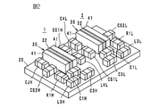
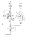
第1実施例である非可逆回路素子は、図1の等価回路に示すように、2ポート型の第1アイソレータ1及び2ポート型の第2アイソレータ2を一体的なモジュールとして構成(図2参照)したものである。第1及び第2アイソレータ1,2は、それぞれ、集中定数型アイソレータであり、マイクロ波磁性体(以下、フェライト32と称する)に、インダクタL1H,L1Lを構成する第1中心電極35とインダクタL2H,L2Lを構成する第2中心電極36とが互いに絶縁状態で交差して配置されている。
第1実施例である非可逆回路素子は、図1の等価回路に示すように、2ポート型の第1アイソレータ1及び2ポート型の第2アイソレータ2を一体的なモジュールとして構成(図2参照)したものである。第1及び第2アイソレータ1,2は、それぞれ、集中定数型アイソレータであり、マイクロ波磁性体(以下、フェライト32と称する)に、インダクタL1H,L1Lを構成する第1中心電極35とインダクタL2H,L2Lを構成する第2中心電極36とが互いに絶縁状態で交差して配置されている。
アイソレータ1,2はともにハイパスタイプであり、第1アイソレータ1の通過周波数帯域は、第2アイソレータ2の通過周波数帯域よりも高く設定されている。第1及び第2アイソレータ1,2の互いの出力部が電気的に接続されて一つの出力端子OUTとされ、それぞれの入力部は入力端子IN1,IN2とされている。さらに、出力端子OUTと第2アイソレータ2の出力部(出力部とは出力ポートP1を意味する。但し、本実施例では出力ポートP1にコンデンサCS1Lが挿入されている)との間にローパスフィルタLPF(インダクタL4LとコンデンサC4LとからなるL型の共振回路)が挿入されている。
以下に、第1及び第2アイソレータ1,2の回路構成を図1を参照して説明する。なお、各回路部品の符号の末尾に、第1アイソレータ1にあっては“H”を、第2アイソレータ2にあっては“L”を付し、以下の説明は第1アイソレータ1について行うが、第2アイソレータ2に関しても同様の構成である。
アイソレータ1は、フェライト32の表面に第1及び第2中心電極35,36(インダクタL1H,L2H)を互いに絶縁状態で交差して配置し、交差部分に永久磁石41(図2、図3参照)から直流磁界(N-S)を印加することにより第1及び第2中心電極35,36を磁気的に結合させ、第1中心電極35の一端を出力ポートP1とし他端を入力ポートP2とし、第2中心電極36の一端を出力ポートP1とし他端をグランドポートP3としている。出力ポートP1は整合用コンデンサCS1Hを介して出力端子OUTに接続され、入力ポートP2は整合用コンデンサCS2Hを介して入力端子IN1に接続されている。
出力ポートP1と入力ポートP2との間には第1中心電極35と並列に整合用コンデンサC1Hが接続されるとともに、抵抗R1HとLC直列共振回路(インダクタL3HとコンデンサC3Hとならなる)とが第1中心電極35と並列に接続されている。出力ポートP1と入力端子IN1との間には、さらに、コンデンサCJHが接続されている。コンデンサCJHは挿入損失とアイソレーションを調整するためのものである。但し、第2アイソレータ2においてコンデンサCJHは省略されている。
本非可逆回路素子は携帯電話の送信用回路に組み込まれる。即ち、出力端子OUTがアンテナANTに整合回路60(インダクタL13とコンデンサC14とからなる)を介して接続される。また、入力端子IN1,IN2が送信側パワーアンプPAにバンドパスフィルタBPFを介して接続される。
前記アイソレータ1,2においては、フェライト32の作用により、ポートP1とポートP2の間が同電位となり、入力ポートP2から高周波信号が入力されると、第2中心電極36や抵抗R1Hにはほとんど電流が流れず、第1中心電極35に電流が流れ、出力ポートP1に出力される。一方、出力ポートP1から高周波信号が入力されると、高周波信号は非可逆作用によって第1中心電極35を通過することなく抵抗R1Hに流れて熱として消費される。即ち、電流が減衰(アイソレーション)される。
入力ポートP2から出力ポートP1へ信号が伝達される動作時において、抵抗R1HやLC直列共振回路(インダクタL3HとコンデンサC3H)にも高周波電流はほとんど流れないため、該LC直列共振回路による損失は無視でき、挿入損失が増大することはない。一方、出力ポートP1に高周波電流が入力されると、抵抗R1HとLC直列共振回路のインピーダンス特性によって広帯域に整合され、アイソレーション特性が向上する。
ここで、前記アイソレータ1,2の特性について図4~図7を参照して説明する。
図4にアイソレーション特性、即ち、出力端子OUTから入力端子IN1へのアイソレーション特性を曲線Aで示し、出力端子OUTから入力端子IN2へのアイソレーション特性を曲線Bで示している。図5に通過特性、即ち、入力端子IN1から出力端子OUTへの通過特性を曲線Aで示し、入力端子IN2から出力端子OUTへの通過特性を曲線Bで示している。
ローパスフィルタLPFの作用により、図5に示すように、824~915MHzで-0.8dB以下、1710~1980MHzで-1.0dB以下の入力合成が実現できている。また、アイソレーション特性は、図4に示すように、824~915MHz及び1710~1980MHzにおいて-10dB以上のレベルを実現している。
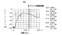
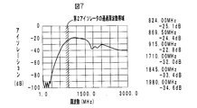
図6に第1アイソレータ1から第2アイソレータへのアイソレーション特性を示し、図7に第2アイソレータから第1アイソレータへのアイソレーション特性を示している。図6及び図7から明らかなように、アイソレータ1,2はそれぞれ斜線を付して示すそれぞれの通過周波数帯域とを切り分けるダイプレクサとしての機能を有し、-20dB以上の信号減衰効果を奏する。
以上のごとく、第1実施例においては、アイソレータ1,2の互いの出力部が電気的に接続されて一つの出力端子OUTとされ、一つの非可逆回路素子として機能する。しかも、出力端子OUTと第2アイソレータ2の出力ポートP1との間にローパスフィルタLPFが挿入されているため、通過周波数帯域が低い第2アイソレータ2の高調波帯域が減衰され、通過周波数帯域が高い第1アイソレータ1との混信が防止される。また、ローパスフィルタLPFの挿入箇所は出力端子OUTと第2アイソレータ2の出力ポートP1との間の1箇所であり、挿入損失の増大や部品点数の増加が抑制される。
つまり、一つのモジュールとして構成されたアイソレータ1,2は、送信回路において、従来のダイプレクサに代わるものであり、かつ、アンテナANT側にインピーダンス整合用のチューナーを設ける必要がなくなる。またアイソレータ1,2は、そのアイソレーション作用によってアンテナANT側の負荷変動(インピーダンス変動)を抑制できる。
次に、前記第1及び第2アイソレータ1,2の具体的な構成について、図2、図3を参照して説明する。図2に示すように、アイソレータ1,2は基板20上に搭載されており、それぞれ、フェライト32と一対の永久磁石41とからなるフェライト・磁石素子30と、チップタイプの各種素子で構成されている。
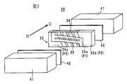
フェライト32には、互いに電気的に絶縁された状態で第1中心電極35及び第2中心電極36が巻回されている。永久磁石41はフェライト32に対して直流磁界を厚み方向(図3の矢印N-S参照)に印加するように、例えば、エポキシ系の接着剤42を介して接着されている。
図3に示すように、第1中心電極35はフェライト32に1ターン巻回されており、一端電極35aが出力ポートP1とされ、他端電極35bが入力ポートP2とされている。第2中心電極36はフェライト32に第1中心電極35と所定の角度で交差した状態で4ターン(なお、ターン数は任意である)巻回されており、一端電極35a(第1中心電極35と共用)が出力ポートP1とされ、他端電極36aがグランドポートP3とされている。なお、図3では煩雑さを避けるためフェライト32の背面側の電極は図示を省略している。
回路基板20は、樹脂基材と導体箔を積層した樹脂基板であり、その上面には、図示しない端子電極が形成されており、これらの端子電極は回路基板20の下面に形成した外部接続用端子IN1,IN2,OUT,GND(図1参照)にビアホール導体(図示せず)を介して接続され、図1に示した等価回路を形成している。
(第2実施例、図8参照)
第2実施例である非可逆回路素子は、図8に示すように、基本的には前記第1実施例と同様の回路構成を有しており、出力端子OUTと第2アイソレータ2の出力部との間に2段のローパスフィルタLPF1,LPF2を挿入している。ローパスフィルタLPF1,LPF2はそれぞれインダクタL4LとコンデンサC4LからなるL型の共振回路を構成している。その作用効果は前記ローパスフィルタLPFと基本的には同様である。
第2実施例である非可逆回路素子は、図8に示すように、基本的には前記第1実施例と同様の回路構成を有しており、出力端子OUTと第2アイソレータ2の出力部との間に2段のローパスフィルタLPF1,LPF2を挿入している。ローパスフィルタLPF1,LPF2はそれぞれインダクタL4LとコンデンサC4LからなるL型の共振回路を構成している。その作用効果は前記ローパスフィルタLPFと基本的には同様である。
(第3実施例、図9参照)
第3実施例である非可逆回路素子は、図9に示すように、基本的には前記第1実施例と同様の回路構成を有しており、出力端子OUTと第2アイソレータ2の出力部との間に挿入したローパスフィルタLPFを、インダクタL4LとコンデンサC4L,C5Lとからなるπ型の共振回路で構成している。π型のローパスフィルタLPFの作用効果もL型の前記ローパスフィルタLPFと同様である。
第3実施例である非可逆回路素子は、図9に示すように、基本的には前記第1実施例と同様の回路構成を有しており、出力端子OUTと第2アイソレータ2の出力部との間に挿入したローパスフィルタLPFを、インダクタL4LとコンデンサC4L,C5Lとからなるπ型の共振回路で構成している。π型のローパスフィルタLPFの作用効果もL型の前記ローパスフィルタLPFと同様である。
(第4実施例、図10参照)
第4実施例である非可逆回路素子は、図10に示すように、基本的には前記第1実施例と同様の回路構成を有しており、出力端子OUTと第2アイソレータ2の出力部との間にストリップラインSLLを挿入している。ストリップラインSLLはローパスフィルタとして機能し、その作用効果は前記ローパスフィルタLPFと同様である。
第4実施例である非可逆回路素子は、図10に示すように、基本的には前記第1実施例と同様の回路構成を有しており、出力端子OUTと第2アイソレータ2の出力部との間にストリップラインSLLを挿入している。ストリップラインSLLはローパスフィルタとして機能し、その作用効果は前記ローパスフィルタLPFと同様である。
(第5実施例、図11参照)
第5実施例である非可逆回路素子は、図11に示すように、基本的には前記第1実施例と同様の回路構成を有しており、図1に示した等価回路からLC直列共振回路(インダクタL3H,L3L、コンデンサC3H,C3L)を省略したものである。出力端子OUTと第2アイソレータ2の出力部との間にはL型の前記ローパスフィルタLPFが挿入されており、その作用効果は前記第1実施例と同様である。
第5実施例である非可逆回路素子は、図11に示すように、基本的には前記第1実施例と同様の回路構成を有しており、図1に示した等価回路からLC直列共振回路(インダクタL3H,L3L、コンデンサC3H,C3L)を省略したものである。出力端子OUTと第2アイソレータ2の出力部との間にはL型の前記ローパスフィルタLPFが挿入されており、その作用効果は前記第1実施例と同様である。
(第6実施例、図12~図16参照)
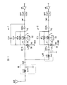
第6実施例である非可逆回路素子は、図12に示すように、第1アイソレータ1において、前記第1実施例などで示したコンデンサC3H及びインダクタL3Hに代えてフィルタ(バンドパスフィルタ)F1が設けられている。フィルタF1は入出力端子51,52、グランド端子53を有し、入出力端子51は抵抗R1Hに接続され、入出力端子52は出力ポートP1に接続され、グランド端子53は入力ポートP2に接続されている。さらに、入力端子IN1は、送受分岐回路素子(デュプレクサDPX、図示しないサーキュレータや表面弾性波素子など)を介して受信部及び送信部に接続されている。本第6実施例における他の構成は前記第1実施例と同様である。
第6実施例である非可逆回路素子は、図12に示すように、第1アイソレータ1において、前記第1実施例などで示したコンデンサC3H及びインダクタL3Hに代えてフィルタ(バンドパスフィルタ)F1が設けられている。フィルタF1は入出力端子51,52、グランド端子53を有し、入出力端子51は抵抗R1Hに接続され、入出力端子52は出力ポートP1に接続され、グランド端子53は入力ポートP2に接続されている。さらに、入力端子IN1は、送受分岐回路素子(デュプレクサDPX、図示しないサーキュレータや表面弾性波素子など)を介して受信部及び送信部に接続されている。本第6実施例における他の構成は前記第1実施例と同様である。
以上の構成からなる第1アイソレータ1においては、入力端子IN1からポートP2に高周波電流が入力される(順方向)と、第2中心電極36や抵抗R1Hにはほとんど電流が流れず、第1中心電極35に電流が流れ、挿入損失が小さく、広帯域で動作する。この順方向動作時において、抵抗R1HやフィルタF1にも高周波電流はほとんど流れないため、これらでの損失は無視でき、挿入損失が増大することはない。
一方、出力端子OUTからポートP1に高周波電流が入力される(逆方向)と、該電流は抵抗R1Hで吸収減衰される。フィルタF1として、非可逆回路素子の通過帯域において、ポートP1及びポートP2と整合のとれた広帯域な特性のものを使用することにより、逆方向特性が広帯域化する。フィルタF1として、送信帯域信号を通過させ、受信帯域信号を減衰させる特性のものを使用することにより、順方向においては送信周波数帯信号を通過させ、逆方向においては送信周波数帯域信号を内部の抵抗R1Hで吸収し減衰させるが、受信周波数帯信号は通過する。
本第6実施例では、このような第1アイソレータ1をアンテナANTとデュプレクサDPXなどの送受分岐回路素子との間に挿入しており、受信部は比較的高い周波数帯とされ、送信部は比較的低い周波数帯とされている。ここでは、アンテナANTで反射した送信波が受信部へ回り込むことが抑制される。これにて、従来のダイプレクサと同等以下のサイズでアンテナANTの負荷変動を抑制した広帯域な送信回路を構成でき、送信回路の小型化と低コスト化に寄与する。
ここで、第6実施例におけるアイソレータ1,2の特性について図13~図16を参照して説明する。
図13にアイソレータ1とアイソレータ2のアイソレーション特性、即ち、出力端子OUTから入力端子IN1へのアイソレーション特性を曲線Aで示し、出力端子OUTから入力端子IN2へのアイソレーション特性を曲線Bで示している。図14にアイソレータ1とアイソレータ2の通過特性、即ち、入力端子IN1から出力端子OUTへの通過特性を曲線Aで示し、入力端子IN2から出力端子OUTへの通過特性を曲線Bで示している。
ローパスフィルタLPFの作用により、図14に示すように、824~915MHzで-0.8dB以下、1710~1980MHzで-1.0dB以下の入力合成が実現できている。また、アイソレーション特性は、図13に示すように、824~915MHzにおいて-10dB以上のレベルを実現している。加えて、フィルタF1を第1アイソレータ1に設けているため、1920~1980MHzにおいて-6dBのアイソレーションを実現し、かつ、受信帯域2110~2170NHzにおいて-1dBの損失に抑えている。
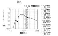
図15に第1アイソレータ1から第2アイソレータ2へのアイソレーション特性を示し、図16に第2アイソレータ2から第1アイソレータ1へのアイソレーション特性を示している。図15及び図16から明らかなように、アイソレータ1,2はそれぞれ斜線を付して示すそれぞれの通過周波数帯域とを切り分けるダイプレクサとしての機能を有し、-15~-20dB以上の信号減衰効果を奏する。
なお、前記第6実施例において、フィルタF1は入出力端子51が抵抗R1Hに接続され、入出力端子52が入力ポートP2に接続され、グランド端子53が出力ポートP1に接続されていてもよい。
(第7実施例、図17参照)
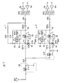
第7実施例である非可逆回路素子は、図17に示すように、第1アイソレータ1のみならず、第2アイソレータ2においても、フィルタ(バンドパスフィルタ)F1を設け、入力端子IN2に送受分岐回路素子(デュプレクサDPX、図示しないサーキュレータや表面弾性波素子など)を介して受信部及び送信部に接続したものである。
第7実施例である非可逆回路素子は、図17に示すように、第1アイソレータ1のみならず、第2アイソレータ2においても、フィルタ(バンドパスフィルタ)F1を設け、入力端子IN2に送受分岐回路素子(デュプレクサDPX、図示しないサーキュレータや表面弾性波素子など)を介して受信部及び送信部に接続したものである。
本第7実施例における第2アイソレータ2の作用は、前記第6実施例での第1アイソレータ1と同様である。
(第8実施例、図18参照)
第8実施例である非可逆回路素子は、図18に示すように、第1及び第2アイソレータ1,2に、それぞれ、フィルタF1と抵抗R1Hに加えて、フィルタF2と抵抗R1Hを並列に接続したものである。フィルタF1,F2をそれぞれ所望の特性のものを選択することにより、非可逆回路素子として必要な特性を得ることができる。特に、送信で用いる所定の周波数帯域が複数あり、かつ、周波数軸上で近接し、一つのフィルタで全ての通過帯域に含めることができない場合に有用である。また、送信で用いる所定の周波数帯域が複数あり、周波数軸上で離れ、これらの複数の送信周波数帯のみを選択的に入力端子から出力端子へ通過させる場合に有用である。
第8実施例である非可逆回路素子は、図18に示すように、第1及び第2アイソレータ1,2に、それぞれ、フィルタF1と抵抗R1Hに加えて、フィルタF2と抵抗R1Hを並列に接続したものである。フィルタF1,F2をそれぞれ所望の特性のものを選択することにより、非可逆回路素子として必要な特性を得ることができる。特に、送信で用いる所定の周波数帯域が複数あり、かつ、周波数軸上で近接し、一つのフィルタで全ての通過帯域に含めることができない場合に有用である。また、送信で用いる所定の周波数帯域が複数あり、周波数軸上で離れ、これらの複数の送信周波数帯のみを選択的に入力端子から出力端子へ通過させる場合に有用である。
(第9実施例、図19及び図20参照)
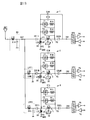
第9実施例である非可逆回路素子は、図19に示すように、フィルタF1,F2をそれぞれ設けた第1アイソレータ1、第2アイソレータ2及び第3アイソレータ3を備えている。第1アイソレータ1の通過周波数帯域は第2アイソレータ2の周波数帯域よりも高く、かつ、第2アイソレータ2の周波数帯域は第3アイソレータ3の周波数帯域よりも高い。そして、各アイソレータ1,2,3のそれぞれの出力部が電気的に接続されて一つの出力端子OUTとされている。なお、図19において、各回路部品の符号の末尾に、第1アイソレータ1にあっては“H”を付し、第2アイソレータ2にあっては“M”を付し、第3アイソレータ3にあっては“L”を付している。
第9実施例である非可逆回路素子は、図19に示すように、フィルタF1,F2をそれぞれ設けた第1アイソレータ1、第2アイソレータ2及び第3アイソレータ3を備えている。第1アイソレータ1の通過周波数帯域は第2アイソレータ2の周波数帯域よりも高く、かつ、第2アイソレータ2の周波数帯域は第3アイソレータ3の周波数帯域よりも高い。そして、各アイソレータ1,2,3のそれぞれの出力部が電気的に接続されて一つの出力端子OUTとされている。なお、図19において、各回路部品の符号の末尾に、第1アイソレータ1にあっては“H”を付し、第2アイソレータ2にあっては“M”を付し、第3アイソレータ3にあっては“L”を付している。
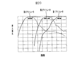
また、出力端子OUTと第2アイソレータ2の出力部との間にローパスフィルタLPF1(バンドパスフィルタであってもよい)が挿入されており、出力端子OUTと第3アイソレータ3の出力部との間にローパスフィルタLPF2が接続されている。本第9実施例における各アイソレータ1,2,3の挿入損失特性は図20に示すとおりであり、三つの周波数帯域を切り替えて送受信することができるように構成されている。
(他の実施例)
なお、本発明に係る非可逆回路素子及びモジュールは前記実施例に限定するものではなく、その要旨の範囲内で種々に変更することができる。
なお、本発明に係る非可逆回路素子及びモジュールは前記実施例に限定するものではなく、その要旨の範囲内で種々に変更することができる。
例えば、フェライト・磁石素子30の構成や第1及び第2中心電極35,36の形状は種々に変更することができる。さらに、容量素子や抵抗素子は回路基板上に外付けしたチップ部品ではなく積層体である回路基板に内蔵されたものであってもよい。
本発明に係るモジュールは、少なくとも二つのアイソレータを含み、必要に応じて出力側に接続される整合回路(60)、入力側に接続されるバンドパスフィルタ(BPF)、デュプレクサ(DPX)やパワーアンプ(PA)が含まれてもよい。
以上のように、本発明は、非可逆回路素子及びモジュールに有用であり、特に、複数の周波数帯域で動作が可能であり、送信回路の部品点数やコストの低減を図り、アンテナ側の負荷変動を抑制できる点で優れている。
1,2,3…アイソレータ
30…フェライト・磁石素子
32…フェライト
35…第1中心電極
36…第2中心電極
41…永久磁石
P1…出力ポート
P2…入力ポート
P3…グランドポート
LPF,LPF1,LPF2…ローパスフィルタ
L4L…インダクタ
C4L,C5L…コンデンサ
SLL…ストリップライン
C1H,C1L…コンデンサ
R1H,R1L…抵抗
IN1,IN2…入力端子
OUT…出力端子
30…フェライト・磁石素子
32…フェライト
35…第1中心電極
36…第2中心電極
41…永久磁石
P1…出力ポート
P2…入力ポート
P3…グランドポート
LPF,LPF1,LPF2…ローパスフィルタ
L4L…インダクタ
C4L,C5L…コンデンサ
SLL…ストリップライン
C1H,C1L…コンデンサ
R1H,R1L…抵抗
IN1,IN2…入力端子
OUT…出力端子
Claims (9)
- 永久磁石により直流磁界が印加されるフェライトに互いに絶縁状態で交差して配置された第1及び第2中心電極を設け、前記第1中心電極の一端を出力ポートとし他端を入力ポートとし、前記第2中心電極の一端を出力ポートとし他端をグランドポートとし、入力ポートと出力ポートとの間に、互いに並列に接続された抵抗素子と容量素子とを直列に接続したハイパスタイプの第1及び第2アイソレータを備え、
第1アイソレータの通過周波数帯域は第2アイソレータの通過周波数帯域よりも高く、
第1及び第2アイソレータの互いの出力部が電気的に接続されて一つの出力端子とされ、
前記出力端子と第2アイソレータの出力ポートとの間にローパスフィルタが挿入されていること、
を特徴とする非可逆回路素子。 - 第1アイソレータ及び/又は第2アイソレータにおいて、前記出力ポート又は前記入力ポートと前記抵抗素子との間に少なくとも一つのフィルタの入出力端子が接続され、かつ、該フィルタのグランド端子が前記入力ポート又は前記出力ポートに接続されていること、を特徴とする請求項1に記載の非可逆回路素子。
- 前記ローパスフィルタはインダクタとコンデンサとからなるL型又はπ型であること、を特徴とする請求項1又は請求項2に記載の非可逆回路素子。
- 前記ローパスフィルタが2段に接続されていること、を特徴とする請求項1又は請求項2に記載の非可逆回路素子。
- 前記ローパスフィルタはストリップラインからなること、を特徴とする請求項1又は請求項2に記載の非可逆回路素子。
- 請求項1~5のいずれかに記載の非可逆回路素子を備え、前記非可逆回路素子の出力端子がアンテナ側に接続されることを特徴とするモジュール。
- 請求項2に記載の非可逆回路素子を備え、
前記フィルタは、送信帯域信号を通過させ、受信帯域信号を減衰させるものであり、
前記フィルタを設けた第1及び/又は第2アイソレータの前記入力ポートに送信信号及び受信信号を分岐させる分岐回路素子を有すること、
を特徴とするモジュール。 - 永久磁石により直流磁界が印加されるフェライトに互いに絶縁状態で交差して配置された第1及び第2中心電極を設け、前記第1中心電極の一端を出力ポートとし他端を入力ポートとし、前記第2中心電極の一端を出力ポートとし他端をグランドポートとし、入力ポートと出力ポートとの間に、互いに並列に接続された抵抗素子と容量素子とを直列に接続したハイパスタイプの第1~第N(Nは2以上の整数)までのアイソレータを備え、
第N-1アイソレータの通過周波数帯域は第Nアイソレータの通過周波数帯域よりも高く、
第1~第Nアイソレータの互いの出力部が電気的に接続されて一つの出力端子とされ、
前記出力端子と第1アイソレータの出力ポートとの間にハイパスフィルタが挿入されており、前記出力端子と第2~第N-1アイソレータの出力ポートとの間にバンドパスフィルタ又はローパスフィルタが挿入されており、前記出力端子と第Nアイソレータの出力ポートとの間にローパスフィルタが挿入されていること、
を特徴とする非可逆回路素子。 - 第1~第Nアイソレータの少なくともいずれかにおいて、前記出力ポート又は前記入力ポートと前記抵抗素子との間に少なくとも一つのフィルタの入出力端子が接続され、かつ、該フィルタのグランド端子が前記入力ポート又は前記出力ポートに接続されていること、を特徴とする請求項8に記載の非可逆回路素子。
Priority Applications (4)
| Application Number | Priority Date | Filing Date | Title |
|---|---|---|---|
| JP2015504243A JP5983859B2 (ja) | 2013-03-08 | 2014-02-24 | 非可逆回路素子及びモジュール |
| CN201480011249.0A CN105009357B (zh) | 2013-03-08 | 2014-02-24 | 不可逆电路元件及模块 |
| US14/838,425 US9711834B2 (en) | 2013-03-08 | 2015-08-28 | Irreversible circuit element and module |
| US15/620,849 US10027008B2 (en) | 2013-03-08 | 2017-06-13 | Irreversible circuit element and module |
Applications Claiming Priority (4)
| Application Number | Priority Date | Filing Date | Title |
|---|---|---|---|
| JP2013046077 | 2013-03-08 | ||
| JP2013-046077 | 2013-03-08 | ||
| JP2013220182 | 2013-10-23 | ||
| JP2013-220182 | 2013-10-23 |
Related Child Applications (1)
| Application Number | Title | Priority Date | Filing Date |
|---|---|---|---|
| US14/838,425 Continuation US9711834B2 (en) | 2013-03-08 | 2015-08-28 | Irreversible circuit element and module |
Publications (1)
| Publication Number | Publication Date |
|---|---|
| WO2014136596A1 true WO2014136596A1 (ja) | 2014-09-12 |
Family
ID=51491118
Family Applications (1)
| Application Number | Title | Priority Date | Filing Date |
|---|---|---|---|
| PCT/JP2014/054288 Ceased WO2014136596A1 (ja) | 2013-03-08 | 2014-02-24 | 非可逆回路素子及びモジュール |
Country Status (4)
| Country | Link |
|---|---|
| US (2) | US9711834B2 (ja) |
| JP (1) | JP5983859B2 (ja) |
| CN (1) | CN105009357B (ja) |
| WO (1) | WO2014136596A1 (ja) |
Cited By (1)
| Publication number | Priority date | Publication date | Assignee | Title |
|---|---|---|---|---|
| JP2019207278A (ja) * | 2018-05-28 | 2019-12-05 | 京セラ株式会社 | 非相反性フィルタ |
Families Citing this family (3)
| Publication number | Priority date | Publication date | Assignee | Title |
|---|---|---|---|---|
| WO2015037693A1 (ja) * | 2013-09-13 | 2015-03-19 | 株式会社村田製作所 | 非可逆回路素子 |
| KR20150035279A (ko) * | 2013-09-27 | 2015-04-06 | 삼성전기주식회사 | 다이플렉서 및 그 제조 방법 |
| JP2018101943A (ja) * | 2016-12-21 | 2018-06-28 | 株式会社村田製作所 | 高周波モジュール |
Citations (4)
| Publication number | Priority date | Publication date | Assignee | Title |
|---|---|---|---|---|
| JPH07283615A (ja) * | 1994-04-07 | 1995-10-27 | Matsushita Electric Ind Co Ltd | 非可逆回路装置 |
| JPH0993004A (ja) * | 1995-09-26 | 1997-04-04 | Murata Mfg Co Ltd | 非可逆回路素子 |
| JP2011176668A (ja) * | 2010-02-25 | 2011-09-08 | Murata Mfg Co Ltd | 非可逆回路素子 |
| WO2014034347A1 (ja) * | 2012-08-28 | 2014-03-06 | 株式会社村田製作所 | 非可逆回路素子 |
Family Cites Families (5)
| Publication number | Priority date | Publication date | Assignee | Title |
|---|---|---|---|---|
| US5973568A (en) | 1998-06-01 | 1999-10-26 | Motorola Inc. | Power amplifier output module for dual-mode digital systems |
| CN101371399B (zh) | 2007-01-18 | 2012-08-29 | 株式会社村田制作所 | 非可逆电路元件及其制造方法 |
| US7532084B2 (en) * | 2007-08-31 | 2009-05-12 | Murata Manufacturing Co., Ltd | Nonreciprocal circuit element |
| JP4640455B2 (ja) * | 2008-06-24 | 2011-03-02 | 株式会社村田製作所 | フェライト・磁石素子、非可逆回路素子及び複合電子部品 |
| CN103608968B (zh) | 2011-06-16 | 2015-08-05 | 株式会社村田制作所 | 不可逆电路元件 |
-
2014
- 2014-02-24 WO PCT/JP2014/054288 patent/WO2014136596A1/ja not_active Ceased
- 2014-02-24 JP JP2015504243A patent/JP5983859B2/ja active Active
- 2014-02-24 CN CN201480011249.0A patent/CN105009357B/zh active Active
-
2015
- 2015-08-28 US US14/838,425 patent/US9711834B2/en active Active
-
2017
- 2017-06-13 US US15/620,849 patent/US10027008B2/en active Active
Patent Citations (4)
| Publication number | Priority date | Publication date | Assignee | Title |
|---|---|---|---|---|
| JPH07283615A (ja) * | 1994-04-07 | 1995-10-27 | Matsushita Electric Ind Co Ltd | 非可逆回路装置 |
| JPH0993004A (ja) * | 1995-09-26 | 1997-04-04 | Murata Mfg Co Ltd | 非可逆回路素子 |
| JP2011176668A (ja) * | 2010-02-25 | 2011-09-08 | Murata Mfg Co Ltd | 非可逆回路素子 |
| WO2014034347A1 (ja) * | 2012-08-28 | 2014-03-06 | 株式会社村田製作所 | 非可逆回路素子 |
Cited By (1)
| Publication number | Priority date | Publication date | Assignee | Title |
|---|---|---|---|---|
| JP2019207278A (ja) * | 2018-05-28 | 2019-12-05 | 京セラ株式会社 | 非相反性フィルタ |
Also Published As
| Publication number | Publication date |
|---|---|
| JPWO2014136596A1 (ja) | 2017-02-09 |
| US9711834B2 (en) | 2017-07-18 |
| JP5983859B2 (ja) | 2016-09-06 |
| CN105009357B (zh) | 2018-02-06 |
| CN105009357A (zh) | 2015-10-28 |
| US20170279175A1 (en) | 2017-09-28 |
| US10027008B2 (en) | 2018-07-17 |
| US20150372365A1 (en) | 2015-12-24 |
Similar Documents
| Publication | Publication Date | Title |
|---|---|---|
| US8253510B2 (en) | Non-reciprocal circuit element | |
| JP5679056B2 (ja) | 非可逆回路素子 | |
| JP5024384B2 (ja) | 非可逆回路素子 | |
| JP5983859B2 (ja) | 非可逆回路素子及びモジュール | |
| JPWO2013168771A1 (ja) | 非可逆回路素子 | |
| JP5748025B2 (ja) | 非可逆回路素子 | |
| JP5874709B2 (ja) | 非可逆回路素子、そのモジュール及び送受信モジュール | |
| US9172125B1 (en) | Non-reciprocal circuit element | |
| CN104081579A (zh) | 不可逆电路元件 | |
| CN104303361B (zh) | 不可逆电路元件 | |
| JP6152896B2 (ja) | 非可逆回路素子 | |
| WO2015093273A1 (ja) | 非可逆回路素子 | |
| JP2012095068A (ja) | 非可逆回路素子 | |
| WO2014115595A1 (ja) | 非可逆回路素子 |
Legal Events
| Date | Code | Title | Description |
|---|---|---|---|
| 121 | Ep: the epo has been informed by wipo that ep was designated in this application |
Ref document number: 14759508 Country of ref document: EP Kind code of ref document: A1 |
|
| ENP | Entry into the national phase |
Ref document number: 2015504243 Country of ref document: JP Kind code of ref document: A |
|
| NENP | Non-entry into the national phase |
Ref country code: DE |
|
| 122 | Ep: pct application non-entry in european phase |
Ref document number: 14759508 Country of ref document: EP Kind code of ref document: A1 |