WO2014125877A1 - ガスバリア性フィルム - Google Patents
ガスバリア性フィルム Download PDFInfo
- Publication number
- WO2014125877A1 WO2014125877A1 PCT/JP2014/050993 JP2014050993W WO2014125877A1 WO 2014125877 A1 WO2014125877 A1 WO 2014125877A1 JP 2014050993 W JP2014050993 W JP 2014050993W WO 2014125877 A1 WO2014125877 A1 WO 2014125877A1
- Authority
- WO
- WIPO (PCT)
- Prior art keywords
- film
- layer
- gas
- gas barrier
- barrier layer
- Prior art date
- Legal status (The legal status is an assumption and is not a legal conclusion. Google has not performed a legal analysis and makes no representation as to the accuracy of the status listed.)
- Ceased
Links
Images

Classifications
-
- B—PERFORMING OPERATIONS; TRANSPORTING
- B32—LAYERED PRODUCTS
- B32B—LAYERED PRODUCTS, i.e. PRODUCTS BUILT-UP OF STRATA OF FLAT OR NON-FLAT, e.g. CELLULAR OR HONEYCOMB, FORM
- B32B27/00—Layered products comprising a layer of synthetic resin
- B32B27/06—Layered products comprising a layer of synthetic resin as the main or only constituent of a layer, which is next to another layer of the same or of a different material
- B32B27/08—Layered products comprising a layer of synthetic resin as the main or only constituent of a layer, which is next to another layer of the same or of a different material of synthetic resin
Definitions
- the present invention relates to a gas barrier film. More specifically, the present invention relates to a gas barrier film excellent in storage stability, particularly storage stability under severe conditions (high temperature and high humidity conditions).
- a gas barrier film formed by laminating a plurality of layers including thin films of metal oxides such as aluminum oxide, magnesium oxide, and silicon oxide on the surface of a plastic substrate or film is used to block various gases such as water vapor and oxygen.
- metal oxides such as aluminum oxide, magnesium oxide, and silicon oxide
- it is widely used for packaging of articles that require the use of, for example, packaging for preventing deterioration of foods, industrial products, pharmaceuticals, and the like.
- Patent Document 1 a technology that does not deteriorate performance even if the base material expands or contracts due to environmental changes by providing a stress relaxation layer above the barrier layer (see Patent Document 1), and hardness between the base material and the inorganic layer.
- Patent Document 2 a technique for improving the flexibility of a film by providing a soft organic layer of 2B or less (see Patent Document 2).
- these methods improve the gas barrier property and bending resistance, the adhesion between the barrier layer and the substrate during long-term storage is not sufficient.
- two primer layers made of a thermosetting resin are laminated between the barrier layer and the base material, and the thermosetting contained in the two layers.
- a gas barrier film in which resins have different compositions has been disclosed (see Patent Document 3).
- Patent Document 3 can withstand long-term storage under high humidity under conditions where the temperature is not so high, but under high temperature and high humidity, the adhesiveness with the barrier layer may decrease due to hydrolysis or the like. There was a problem of deterioration.
- the present invention has been made in view of the above circumstances, and an object thereof is to provide a gas barrier film having excellent storage stability, particularly storage stability under severe conditions (high temperature and high humidity conditions).
- the present inventor conducted intensive research to solve the above problems.
- the first anchor layer containing the curable resin and the active energy ray-curable resin between the resin base material and the barrier layer and the surface hardness measured by the nanoindentation method are the first
- the present inventors have found that the above problem can be solved by a gas barrier film containing a second anchor layer different from the anchor layer of the present invention, and have completed the present invention.
- the present invention includes a resin base material, a first anchor layer containing a curable resin, an active energy ray-curable resin, and a surface hardness measured by a nanoindentation method is the first anchor layer.
- a gas barrier film comprising a different second anchor layer and a barrier layer containing an inorganic compound in this order.
- a gas barrier film excellent in storage stability, particularly storage stability under severe conditions (high temperature and high humidity conditions) is provided.
- FIG. 1 is a gas barrier film
- 2 is an anchor layer-formed substrate
- 3 is a barrier layer
- 31 is a manufacturing apparatus
- 32 is a delivery roller
- 33, 34, 35 and 36 are transport rollers
- 39 and 40 are film forming rollers
- 42 is a plasma generating power source
- 43 and 44 are magnetic field generators
- 45 is a winding roller.
- the present invention includes a resin substrate, a first anchor layer containing a curable resin, an ultraviolet curable resin, and a second hardness different from that of the first anchor layer as measured by a nanoindentation method.
- a gas barrier film comprising an anchor layer and a barrier layer containing an inorganic compound in this order.
- Patent Document 1 a technology that does not deteriorate the performance even when the base material expands / shrinks due to environmental changes by providing a stress relaxation layer above the barrier layer (the above-mentioned Patent Document 1), and the hardness between the base material and the inorganic layer.
- Patent Document 2 a technique for improving the flexibility of the film by providing a soft organic layer of 2B or less (Patent Document 2).
- Patent Document 3 a technique of laminating two layers of primers having different compositions between the barrier layer and the base material is disclosed (Patent Document 3).
- Patent Document 3 can withstand long-term storage under high humidity under conditions where the temperature is not so high, but under high temperature and high humidity, the adhesiveness with the barrier layer is reduced due to hydrolysis or the like. There was a problem of deterioration.
- the inventor of the present invention has a first anchor layer and a second anchor layer having different surface hardness laminated between a resin base material and a barrier layer. It was found that this gas barrier film exhibited high barrier properties with almost no cracking or peeling of the barrier layer. Further, in the conventional gas barrier film, as a result of hygroscopic expansion and thermal expansion, phenomena such as a decrease in transmittance and an increase in HAZE due to the deformation of the substrate were observed. It was found that the characteristics were hardly impaired and high transmittance and HAZE could be maintained.
- gas barrier film of the present invention is excellent in storage stability, particularly storage stability under high temperature and high humidity is unknown, but is considered to be as follows.
- a chemical deposition method (plasma CVD) is used in which an organic silicon compound such as tetraethoxysilane (TEOS) is used and a film is formed on a substrate while being oxidized with oxygen plasma under reduced pressure.
- vapor phase methods such as chemical vapor deposition (chemical vapor deposition) and physical deposition methods (vacuum evaporation method and sputtering method) that vaporize metal Si using a semiconductor laser and deposit it on the substrate in the presence of oxygen.
- chemical vapor deposition chemical vapor deposition
- physical deposition methods vacuum evaporation method and sputtering method
- the configuration of the present invention it is also effective for the deformation of the resin base material generated by the gas phase method as described above.
- This effect is more remarkable in a resin base material having a large expansion and contraction due to heat, such as a triacetyl cellulose (TAC) film or a polycarbonate (PC) film. Therefore, it is possible to provide a gas barrier film that is suitable for optical applications such as OLED and has low retardation and excellent long-term storage stability.
- TAC triacetyl cellulose
- PC polycarbonate
- X to Y indicating a range means “X or more and Y or less”, “weight” and “mass”, “weight%” and “mass%”, “part by weight” and “weight part”. “Part by mass” is treated as a synonym. Unless otherwise specified, measurement of operation and physical properties is performed under conditions of room temperature (20 to 25 ° C.) / Relative humidity 40 to 50%.
- the gas barrier film of the present invention has a resin base material, a first anchor layer, a second anchor layer, and a barrier layer in this order.
- the gas barrier film of the present invention may further contain other members.
- the gas barrier film of the present invention is, for example, between the resin base material and the first anchor layer, between the first anchor layer and the second anchor layer, between the second anchor layer and the barrier layer, Another member may be provided on the barrier layer or on the other surface of the base material on which the barrier layer is not formed.
- the other members are not particularly limited, and members used for conventional gas barrier films can be used similarly or appropriately modified. Specific examples include a smooth layer, an anchor coat layer, an overcoat layer, a bleed-out prevention layer, a protective layer, a functional layer of a moisture absorption layer and an antistatic layer, and the like.
- the gas barrier unit having the first anchor layer, the second anchor layer, and the barrier layer may be formed on one surface of the resin base material, or formed on both surfaces of the resin base material. May be.
- the gas barrier unit may include a layer that does not necessarily have a gas barrier property.
- a plastic film or a plastic sheet is used as a resin substrate, and a film or sheet made of a colorless and transparent resin is preferably used.
- the plastic film to be used is not particularly limited in material, thickness and the like as long as it can hold the first anchor layer, the second anchor layer, the barrier layer, and the like, and can be appropriately selected according to the purpose of use.
- Specific examples of the plastic film include polyester resin, methacrylic resin, methacrylic acid-maleic acid copolymer, polystyrene resin, transparent fluororesin, polyimide, fluorinated polyimide resin, polyamide resin, polyamideimide resin, and polyetherimide.
- Resin cellulose acylate resin, polyurethane resin, polyether ether ketone resin, polycarbonate resin, alicyclic polyolefin resin, polyarylate resin, polyether sulfone resin, polysulfone resin, cycloolefin copolymer, fluorene ring modified polycarbonate resin, alicyclic modification
- thermoplastic resins such as polycarbonate resin, fluorene ring-modified polyester resin, and acryloyl compound.
- the resin base material is preferably made of a heat resistant material. Specifically, a resin base material having a linear expansion coefficient of 15 ppm / K or more and 100 ppm / K or less and a glass transition temperature (Tg) of 100 ° C. or more and 300 ° C. or less is used.
- Tg glass transition temperature
- the base material satisfies the requirements for use as a laminated film for electronic parts and displays. That is, when the gas barrier film of the present invention is used for these applications, the gas barrier film may be exposed to a process at 150 ° C. or higher.
- the substrate dimensions are not stable when the gas barrier film is passed through the temperature process as described above, and thermal expansion and contraction occur. Inconvenience that the shut-off performance is deteriorated or a problem that the thermal process cannot withstand is likely to occur. If it is less than 15 ppm / K, the film may break like glass and the flexibility may deteriorate.
- Polyolefin for example, ZEONOR (registered trademark) 1600: 160 ° C) manufactured by Nippon Zeon Co., Ltd., polyarylate (PAr: 210 ° C), polyethersulfone (PES: 220 ° C), polysulfone (PSF: 190 ° C), cycloolefin Copolymer (COC: Compound described in JP-A No. 2001-150584: 162 ° C.), polyimide (for example, Neoprim (registered trademark): 260 ° C. manufactured by Mitsubishi Gas Chemical Co., Ltd.), fluorene ring-modified polycarbonate (BCF-PC: special Kai 2000-227603 Compound described in JP-A No.
- the gas barrier film according to the present invention is used in combination with, for example, a polarizing plate, it is preferable to arrange the gas barrier film so that the barrier layer of the gas barrier film faces the inside of the cell. More preferably, the barrier layer of the gas barrier film is disposed on the innermost side of the cell (adjacent to the element). At this time, since the gas barrier film is disposed inside the cell from the polarizing plate, the retardation value of the gas barrier film is important.
- the usage form of the gas barrier film in such an embodiment includes a gas barrier film using a resin base film having a retardation value of 10 nm or less and a circularly polarizing plate (1 ⁇ 4 wavelength plate + (1 ⁇ 2 wavelength plate) + A linear polarizing plate in combination with a gas barrier film using a resin base film having a retardation value of 100 nm to 180 nm, which can be used as a quarter wavelength plate. Is preferred.
- Examples of the resin base film having a retardation value of 10 nm or less include a triacetyl cellulose film (manufactured by Konica Minolta Advanced Layer Co., Ltd .: Konica Minolta Tack KC6UY, Fuji Film Co., Ltd .: Fujitac (registered trademark)), polycarbonate film, and the like.
- the quarter wavelength plate a film adjusted to a desired retardation value by appropriately stretching the above film can be used.
- a triacetyl cellulose film and a polycarbonate film are preferable, and a triacetyl cellulose film is more preferable.
- the substrate is preferably transparent. That is, the light transmittance is usually 80% or more, preferably 85% or more, and more preferably 90% or more.
- the light transmittance is calculated by measuring the total light transmittance and the amount of scattered light using the method described in JIS K7105: 1981, that is, using an integrating sphere light transmittance measuring device, and subtracting the diffuse transmittance from the total light transmittance. can do.
- an opaque material can be used as the base material.
- the opaque material include polyimide, polyacrylonitrile, and known liquid crystal polymers.
- the thickness of the base material used for the gas barrier film according to the present invention is not particularly limited because it is appropriately selected depending on the application, but is typically 1 to 800 ⁇ m, preferably 10 to 200 ⁇ m.
- These plastic films may have functional layers such as a transparent conductive layer and a primer layer.
- As the functional layer in addition to those described above, those described in paragraph numbers “0036” to “0038” of JP-A-2006-289627 (corresponding to US Patent Application Publication No. 2006/251905) are preferably used. Can be adopted.
- the substrate preferably has a high surface smoothness.
- the surface smoothness those having an average surface roughness (Ra) of 2 nm or less are preferable. Although there is no particular lower limit, it is practically 0.01 nm or more. If necessary, both surfaces of the substrate, at least the side on which the barrier layer is provided, may be polished to improve smoothness.
- the resin base material listed above may be an unstretched film or a stretched film.
- a stretched film is preferable, a stretched triacetyl cellulose film, and a stretched polycarbonate film are more preferable, and stretched.
- a triacetyl cellulose film is more preferable.
- the barrier layer is formed by a vacuum film formation method such as a chemical vapor deposition method, it is preferable to use a stretched film.
- the resin substrate used in the present invention can be produced by a conventionally known general method.
- an unstretched substrate that is substantially amorphous and not oriented can be produced by melting a resin as a material with an extruder, extruding it with an annular die or a T-die, and quenching.
- the unstretched resin base material is uniaxially stretched, tenter-type sequential biaxial stretching, tenter-type simultaneous biaxial stretching, tubular simultaneous biaxial stretching, and other known methods, such as the base material flow (vertical axis) direction
- a stretched resin substrate can be produced by stretching in a direction perpendicular to the flow direction of the substrate (horizontal axis).
- the draw ratio in this case can be appropriately selected according to the resin used as the raw material of the resin base material, but is preferably 2 to 10 times in the vertical axis direction and the horizontal axis direction.
- At least the first anchor layer according to the present invention on the side where the first anchor layer is provided is known various treatments for improving adhesion, such as corona discharge treatment, flame treatment, oxidation treatment, or plasma treatment, and smoothing described later. Layer stacking or the like may be performed, and it is preferable to combine the above treatments as necessary.
- the gas barrier film of the present invention includes a first anchor layer containing a curable resin and an active energy ray curable resin on the top of a resin substrate (between the resin substrate and the barrier layer), and a nanoindene. It has the 2nd anchor layer in which the surface hardness measured by a tentation method differs from the said 1st anchor layer in this order. By setting it as such a structure, even if it preserve
- the first anchor layer includes a curable resin.
- the curable resin is not particularly limited, and the active energy ray curable material is irradiated with an active energy ray such as an ultraviolet ray, an electron beam, an X ray, an ⁇ ray, a ⁇ ray, a ⁇ ray, and a neutron ray to be cured. Examples thereof include an active energy ray curable resin obtained and a thermosetting resin obtained by curing by heating a thermosetting material. These curable resins may be used alone or in combination of two or more.
- the active energy ray-curable material examples include a composition containing an acrylate compound, a composition containing an acrylate compound and a mercapto compound containing a thiol group, epoxy acrylate, urethane acrylate, polyester acrylate, polyether acrylate, polyethylene
- examples thereof include compositions containing polyfunctional acrylate monomers such as glycol acrylate and glycerol methacrylate.
- OPSTAR registered trademark
- JSR Corporation JSR Corporation. It is also possible to use any mixture of the above-mentioned compositions, and an active energy ray-curable material containing a reactive monomer having at least one photopolymerizable unsaturated bond in the molecule. If there is no particular limitation.
- Examples of reactive monomers having at least one photopolymerizable unsaturated bond in the molecule include methyl acrylate, ethyl acrylate, n-propyl acrylate, isopropyl acrylate, n-butyl acrylate, isobutyl acrylate, tert-butyl acrylate, and n-pentyl.
- active energy ray curing also includes polyester resins, silicone resins, and the like having an active energy ray-curable functional group that causes a curing reaction when irradiated with active energy rays such as ethylenically unsaturated double bonds. It can be used as a property material.
- composition containing the active energy ray-curable material contains a photopolymerization initiator.
- photopolymerization initiator examples include benzophenone, methyl o-benzoylbenzoate, 4,4-bis (dimethylamine) benzophenone, 4,4-bis (diethylamine) benzophenone, ⁇ -amino acetophenone, 4,4-dichloro Benzophenone, 4-benzoyl-4-methyldiphenyl ketone, dibenzyl ketone, fluorenone, 2,2-diethoxyacetophenone, 2,2-dimethoxy-2-phenylacetophenone, 2-hydroxy-2-methylpropiophenone, p- tert-Butyldichloroacetophenone, thioxanthone, 2-methylthioxanthone, 2-chlorothioxanthone, 2-isopropylthioxanthone, diethylthioxanthone, benzyldimethyl ketal, benzylmethoxyethyl acetal, benzo Methyl ether
- the active energy ray-curable material may be a commercially available product or a synthetic product.
- commercially available products include, for example, OPSTAR (registered trademark) Z7527 (manufactured by JSR Corporation), MP-6103 (manufactured by Washin Chemical Industry Co., Ltd.), Unidic (registered trademark) V-4025 (urethane acrylate, DIC Corporation) And Aika Eyetron Z842-1 (manufactured by Aika Industry Co., Ltd.).
- thermosetting materials include thermosetting urethane resins composed of acrylic polyols and isocyanate prepolymers, phenol resins, melamine resins, urea melamine resins, epoxy resins, unsaturated polyester resins, silicon resins, and polyamidoamines. -Epichlorohydrin resins, mixtures of polyester resins and isocyanate resins, and the like.
- the thermosetting material may be a commercially available product or a synthetic product.
- commercially available products include, for example, TutProm Series (Organic Polysilazane) manufactured by Clariant, SP COAT heat-resistant clear paint manufactured by Ceramic Co., Ltd., Nanohybrid Silicone manufactured by Adeka, Unidick manufactured by DIC Corporation ( (Registered trademark) V-8000 series, EPICLON (registered trademark) EXA-4710 (super high heat resistance epoxy resin), silicon resin X-12-2400 (trade name) manufactured by Shin-Etsu Chemical Co., Ltd., manufactured by Nitto Boseki Co., Ltd.
- examples include inorganic / organic nanocomposite material SSG coat.
- the first anchor layer preferably contains an active energy ray curable resin.
- the method for forming the first anchor layer is not particularly limited, but a bar coating method using a wire bar or the like, a spin coating method, a spray method, a blade coating method, a dip method, or a gravure printing method.
- a wet coating method such as vapor deposition or a dry coating method such as vapor deposition to form a coating film
- active energy such as visible light, infrared light, ultraviolet light, X-rays, ⁇ -rays, ⁇ -rays, ⁇ -rays, and electron beams
- a method in which the coating film is cured and formed by irradiation with rays and / or heating is preferred.
- an ultra-high pressure mercury lamp, a high-pressure mercury lamp, a low-pressure mercury lamp, a carbon arc, a metal halide lamp or the like is used, and ultraviolet rays in a wavelength region of preferably 100 to 400 nm, more preferably 200 to 400 nm are irradiated.
- a method of irradiating an electron beam having a wavelength region of 100 nm or less emitted from a scanning or curtain type electron beam accelerator is preferably 0.1 to 1 J / cm 2 .
- examples of the heat curing method include a method of heating using an oven, a hot air oven, a hot air dryer, a hot plate, or the like.
- the heating temperature for heating is preferably 50 to 150 ° C.
- the heating time is preferably 30 seconds to 5 minutes.
- Solvents used when forming the first anchor layer using a coating solution in which a curable material is dissolved or dispersed in a solvent include methanol, ethanol, n-propyl alcohol, isopropyl alcohol, ethylene glycol, propylene glycol, etc.
- the first anchor layer can contain additives such as a thermoplastic resin, an antioxidant, an ultraviolet absorber, and a plasticizer, if necessary, in addition to the curable material described above. Further, it may contain an appropriate resin, additives such as a silane coupling agent and metal oxide particles for improving the film formability, preventing the occurrence of pinholes in the film, and adjusting the surface hardness of the film.
- the thermoplastic resin include cellulose derivatives such as acetylcellulose, nitrocellulose, acetylbutylcellulose, ethylcellulose and methylcellulose, vinyl acetate and copolymers thereof, vinyl chloride and copolymers thereof, vinylidene chloride and copolymers thereof and the like.
- Examples include resins, acetal resins such as polyvinyl formal and polyvinyl butyral, acrylic resins and copolymers thereof, acrylic resins such as methacrylic resins and copolymers thereof, polystyrene resins, polyamide resins, linear polyester resins, and polycarbonate resins.
- the thickness of the first anchor layer is not particularly limited, but is preferably 0.025 to 10 ⁇ m, more preferably 0.5 to 4 ⁇ m from the viewpoint of suppressing curling of the gas barrier film.
- the surface hardness (hereinafter also simply referred to as “SHA”) of the first anchor layer measured by the nanoindentation method is 0.15 to 0.00 from the viewpoint of obtaining the above-described effect of the present invention more efficiently. It is preferably 4 GPa, more preferably 0.25 to 0.4 GPa.
- the nanoindentation method is a method in which the indenter is continuously loaded and unloaded with a very small load, and the hardness and elastic modulus are measured from the obtained load-displacement curve.
- the nanoindentation method is a measurement of indentation hardness at the nano level by adding an indentation hardness measurement module (configured with a transducer and an indentation tip) to an atomic force microscope (AFM). It is a measuring method that can be performed. While applying a load of ⁇ N or less, a diamond indenter is pushed into the sample, and the indentation depth is measured with nanometer accuracy. A load-displacement curve diagram can be obtained from this measurement, and the properties of the material relating to elasto-plastic deformation can be quantitatively evaluated. In the case of a thin film, in order to perform measurement without being affected by the base material, it is necessary to push in to a depth of 1/10 to 1/3 of the film thickness.
- AFM atomic force microscope
- the surface hardness of the first anchor layer, the second anchor layer, and the barrier layer is measured using a Triscope from Hysitoron attached to a scanning probe microscope (SPI3800N from Seiko Instruments Inc.). .
- the working indenter is a cube corner tip (90 °).
- the SHa can be controlled by the type of curable resin, conditions for curing, and the like.
- the second anchor layer contains an active energy ray-curable resin, and the surface hardness measured by the nanoindentation method is different from that of the first anchor layer.
- active energy ray-curable resin contained in the second anchor layer are the same as those described in the section of the first anchor layer, and the description thereof is omitted here.
- the active energy ray-curable resin used for the second anchor layer may be a commercially available product or a synthetic product.
- Examples of commercially available active energy ray-curable resins used for the second anchor layer include, for example, OPSTAR (registered trademark) Z7527 (manufactured by JSR Corporation), Aika Eyetron Z842-1 (manufactured by Aika Industry Co., Ltd.) Etc.
- UV curable resins ultraviolet curable resins
- the active energy ray-curable resin in addition to the active energy ray-curable resin, it contains additives such as a thermoplastic resin, an antioxidant, an ultraviolet absorber, and a plasticizer as necessary. Can do. Further, it may contain an appropriate resin, additives such as a silane coupling agent and metal oxide particles for improving the film formability, preventing the occurrence of pinholes in the film, and adjusting the surface hardness of the film.
- the method for forming the second anchor layer is also the same as the method described in the section of the first anchor layer, and the description is omitted here.
- the film thickness of the second anchor layer is not particularly limited, but is preferably 0.025 to 10 ⁇ m, more preferably 0.5 to 4 ⁇ m.
- the film thickness of the second anchor layer is more preferably smaller than the film thickness of the first anchor layer. With such a film thickness relationship, the effects of the present invention can be obtained more efficiently.
- the surface hardness (hereinafter also simply referred to as SHb) of the second anchor layer measured by the nanoindentation method is different from the surface hardness (SHA) of the first anchor layer (SHa ⁇ SHb). Specifically, it is preferably 0.15 to 0.4 GPa, more preferably 0.25 to 0.4 GPa.
- the SHb can be controlled by the type of active energy ray-curable resin, the conditions for curing, and the like.
- the first anchor layer and the second anchor layer are preferably smooth because a barrier layer is provided on the top.
- the surface roughness (Ra value) is preferably 0.3 to 3 nm, and more preferably 0.5 to 1.5 nm. If the thickness is smaller than 0.3 nm, the surface is too smooth, roll conveyance is deteriorated, and there is a possibility that the barrier layer formation by the CVD method may be hindered. On the other hand, if the thickness is larger than 3 nm, minute defects are likely to be formed in the barrier layer, and the gas barrier property and adhesion may be lowered.
- the surface roughness is calculated from an uneven cross-sectional curve continuously measured with an AFM (Atomic Force Microscope), for example, DI3100 manufactured by Digital Instruments, with a detector having a stylus with a minimum tip radius, and the minimum tip This is the roughness related to the amplitude of fine irregularities, measured many times in a section whose measurement direction is several tens of ⁇ m with a radius stylus.
- AFM Acoustic Force Microscope
- an intermediate layer such as an adhesive layer may be further provided between the first anchor layer and the second anchor layer.
- an intermediate layer such as an adhesive layer
- a form in which the first anchor layer and the second anchor layer are in contact with each other without an intermediate layer is preferable.
- the total film thickness of the first anchor layer and the second anchor layer is preferably in the range of 0.3 to 20 ⁇ m, and more preferably in the range of 0.5 to 10 ⁇ m. Within such a range, curling of the gas barrier film can be suppressed.
- said 1st anchor layer and 2nd anchor layer can also suppress the phenomenon (bleed out) which an unreacted oligomer etc. transfer from a resin base material to a barrier layer, and is contaminated.
- the barrier layer according to the present invention formed on the second anchor layer includes an inorganic compound. Although it does not specifically limit as an inorganic compound contained in a barrier layer, For example, a metal oxide, a metal nitride, a metal carbide, a metal oxynitride, or a metal oxycarbide is mentioned.
- oxides, nitrides, carbides, oxynitrides or oxycarbides containing one or more metals selected from Si, Al, In, Sn, Zn, Ti, Cu, Ce and Ta in terms of gas barrier performance are preferably used, and an oxide, nitride or oxynitride of a metal selected from Si, Al, In, Sn, Zn and Ti is more preferable, and in particular, an oxide of at least one of Si and Al, Nitride or oxynitride is preferred.
- suitable inorganic compounds include composites such as silicon oxide, silicon nitride, silicon oxynitride, silicon carbide, silicon oxycarbide, aluminum oxide, titanium oxide, and aluminum silicate. You may contain another element as a secondary component.
- the content of the inorganic compound contained in the barrier layer is not particularly limited, but is preferably 50% by weight or more, more preferably 80% by weight or more, and more preferably 95% by weight or more in the barrier layer. It is preferably 98% by weight or more, and most preferably 100% by weight (that is, the barrier layer is made of an inorganic compound).
- the barrier layer contains an inorganic compound and thus has a gas barrier property.
- the gas barrier property of the barrier layer is calculated with a laminate in which the barrier layer is formed on the substrate, the water vapor transmission rate (WVTR) measured by the method described in Examples below is 0.1 g / preferably (m 2 ⁇ day) or less, more preferably 0.01g / (m 2 ⁇ day) or less.
- the method for forming the barrier layer is not particularly limited, but includes a vacuum film-forming method such as physical vapor deposition (PVD method), chemical vapor deposition (chemical vapor deposition, hereinafter also simply referred to as CVD), or a silicon compound.
- PVD method physical vapor deposition
- CVD chemical vapor deposition
- silicon compound a silicon compound.
- a method in which a coating film formed by applying a liquid to be formed is subjected to a modification treatment (hereinafter also simply referred to as a coating method) is preferable.
- the physical vapor deposition method is a method of depositing a target material, for example, a thin film such as a carbon film, on the surface of the material in a gas phase by a physical method.
- a sputtering method DC sputtering, RF sputtering
- Ion beam sputtering, magnetron sputtering, etc. vacuum deposition method, ion plating method and the like.
- Sputtering is a method in which a target is placed in a vacuum chamber, a rare gas element (usually argon) ionized by applying a high voltage is collided with the target, and atoms on the target surface are ejected and adhered to the substrate.
- a reactive sputtering method may be used in which an inorganic layer is formed by causing nitrogen and oxygen gas to flow into the chamber to react the element ejected from the target with argon gas with nitrogen and oxygen. .
- Chemical vapor deposition (chemical vapor deposition, Chemical Vapor Deposition) supplies a raw material gas containing the desired thin film components onto a resin substrate, and the film is formed by a chemical reaction on the surface of the resin substrate or in the gas phase. It is a method of depositing. In addition, for the purpose of activating the chemical reaction, there is a method of generating plasma or the like.
- Known CVD such as thermal CVD method, catalytic chemical vapor deposition method, photo CVD method, vacuum plasma CVD method, atmospheric pressure plasma CVD method, etc. The method etc. are mentioned. Although not particularly limited, it is preferable to apply the plasma CVD method from the viewpoint of the film formation speed and the processing area.
- the conditions such as the raw material (also referred to as raw material) metal compound, decomposition gas, decomposition temperature, input power, etc. are selected. Therefore, the target compound can be produced, which is preferable.
- silicon oxide is generated.
- highly active charged particles and active radicals exist in the plasma space at a high density, so that multistage chemical reactions are accelerated at high speed in the plasma space, and the elements present in the plasma space are thermodynamic. This is because it is converted into an extremely stable compound in a very short time.
- a raw material compound used in the vacuum film-forming method it is preferable to use a silicon compound, a titanium compound, and an aluminum compound.
- a raw material compound it is preferable to use a silicon compound, a titanium compound, and an aluminum compound.
- silicon compounds silane, tetramethoxysilane, tetraethoxysilane, tetra n-propoxysilane, tetraisopropoxysilane, tetra n-butoxysilane, tetra t-butoxysilane, dimethyldimethoxysilane, dimethyldiethoxysilane, Examples include diethyldimethoxysilane and diphenyldimethoxysilane.
- titanium compounds include titanium methoxide, titanium ethoxide, titanium isopropoxide, titanium tetraisoporopoxide, titanium n-butoxide, and the like.
- a decomposition gas for decomposing a raw material gas containing these metals to obtain an inorganic compound hydrogen gas, methane gas, acetylene gas, carbon monoxide gas, carbon dioxide gas, nitrogen gas, ammonia gas, nitrous oxide
- examples include gas, nitrogen oxide gas, nitrogen dioxide gas, oxygen gas, and water vapor.
- the decomposition gas may be mixed with an inert gas such as argon gas or helium gas.
- a decomposition gas for decomposing a raw material gas containing these metals to obtain an inorganic compound hydrogen gas, methane gas, acetylene gas, carbon monoxide gas, carbon dioxide gas, nitrogen gas, ammonia gas, nitrous oxide
- examples include gas, nitrogen oxide gas, nitrogen dioxide gas, oxygen gas, and water vapor.
- the decomposition gas may be mixed with an inert gas such as argon gas or helium gas.
- the barrier layer according to the present invention may be formed by a method (coating method) in which a coating film formed by applying a liquid containing a silicon compound is reformed.
- the silicon compound used in the coating method is not particularly limited as long as a coating solution containing a silicon compound can be prepared.
- the silicon compound is not particularly limited as long as a coating liquid containing a silicon compound can be prepared.
- perhydropolysilazane perhydropolysilazane, organopolysilazane, silsesquioxane, tetramethylsilane, trimethylmethoxysilane, dimethyldimethoxysilane, methyltrimethoxysilane, trimethylethoxysilane, dimethyldiethoxysilane, methyltriethoxysilane, Examples thereof include tetramethoxysilane.
- polysilazane such as perhydropolysilazane and organopolysilazane; polysiloxane such as silsesquioxane, etc. are preferable in terms of film formation, fewer defects such as cracks, and less residual organic matter, and high gas barrier performance.
- Polysilazane is more preferable, and perhydropolysilazane is particularly preferable because the barrier performance is maintained even when bent and under high temperature and high humidity conditions.
- Polysilazane is a polymer having a silicon-nitrogen bond, such as SiO 2 , Si 3 N 4 having a bond such as Si—N, Si—H, or N—H, and ceramics such as both intermediate solid solutions SiO x N y. It is a precursor inorganic polymer.
- the polysilazane preferably has the following structure.
- R 1 , R 2 and R 3 are each independently a hydrogen atom, a substituted or unsubstituted alkyl group, aryl group, vinyl group or (trialkoxysilyl) alkyl group. .
- R 1 , R 2 and R 3 may be the same or different.
- examples of the alkyl group include linear, branched or cyclic alkyl groups having 1 to 8 carbon atoms.
- n is an integer
- the polysilazane having the structure represented by the general formula (I) is determined to have a number average molecular weight of 150 to 150,000 g / mol. preferable.
- one of preferred embodiments is perhydropolysilazane in which all of R 1 , R 2 and R 3 are hydrogen atoms.
- Perhydropolysilazane is presumed to have a linear structure and a ring structure centered on 6- and 8-membered rings.
- the number average molecular weight (Mn) is about 600 to 2000 (polystyrene conversion), and there are liquid or solid substances, and the state varies depending on the molecular weight.
- Polysilazane is commercially available in the form of a solution dissolved in an organic solvent, and the commercially available product can be used as it is as a coating solution for forming a polysilazane layer.
- Examples of commercially available polysilazane solutions include AQUAMICA (registered trademark) NN120-10, NN120-20, NAX120-20, NN110, NN310, NN320, NL110A, NL120A, NL120-20, NL150A, and NP110 manufactured by AZ Electronic Materials Co., Ltd. NP140, SP140 and the like.
- the film thickness (dry film thickness) of the barrier layer is not particularly limited, but the film thickness per layer of the barrier layer is preferably 20 to 3000 nm, more preferably 50 to 2500 nm, and more preferably 100 to Particularly preferred is 1000 nm. With such a film thickness, the gas barrier film can exhibit excellent gas barrier properties and the effect of suppressing / preventing cracking during bending. In addition, when the barrier layer formed by said plasma CVD method is comprised from 2 or more layers, it is preferable that each barrier layer has a film thickness as mentioned above.
- the barrier layer can be formed, for example, by the method described in paragraphs “0035” to “0058” of JP2012-131194A.
- the barrier layer preferably contains carbon, silicon, and oxygen as constituent elements.
- a more preferable form is a layer that satisfies the following requirements (i) to (iii).
- the barrier layer comprises (i) a distance (L) from the surface of the barrier layer in the film thickness direction of the barrier layer and a ratio of the amount of silicon atoms to the total amount of silicon atoms, oxygen atoms, and carbon atoms (silicon A silicon distribution curve showing a relationship with the atomic ratio), an oxygen distribution curve showing a relationship between the L and the ratio of the amount of oxygen atoms to the total amount of silicon atoms, oxygen atoms, and carbon atoms (atomic ratio of oxygen), and 90% or more of the thickness of the barrier layer (upper limit) in the carbon distribution curve showing the relationship between the L and the ratio of the amount of carbon atoms to the total amount of silicon atoms, oxygen atoms, and carbon atoms (the atomic ratio of carbon) : 100%) in the order of (atomic ratio of oxygen), (atomic ratio of silicon), and (atomic ratio of carbon) (atomic ratio is preferably O> Si> C).
- the gas barrier property and flexibility of the resulting gas barrier film may be insufficient.
- the relationship of the above (atomic ratio of oxygen), (atomic ratio of silicon) and (atomic ratio of carbon) is at least 90% or more (upper limit: 100%) of the thickness of the barrier layer. ) And more preferably at least 93% or more (upper limit: 100%).
- “at least 90% or more of the thickness of the barrier layer” does not need to be continuous in the barrier layer, and only needs to satisfy the above-described relationship at a portion of 90% or more.
- the barrier layer has (ii) the carbon distribution curve has at least two extreme values.
- the barrier layer preferably has at least three extreme values in the carbon distribution curve, and more preferably has at least four extreme values, but may have five or more extreme values.
- the extreme value of the carbon distribution curve is 1 or less, the gas barrier property may be insufficient when the obtained gas barrier film is bent.
- the upper limit of the number of extreme values in the carbon distribution curve is not particularly limited, but is preferably 30 or less, more preferably 25 or less, for example. Since the number of extreme values is also caused by the film thickness of the barrier layer, it cannot be specified unconditionally.
- the distance from the surface of the barrier layer in the film thickness direction of the barrier layer at one extreme value of the carbon distribution curve and the extreme value adjacent to the extreme value is preferably 200 nm or less, more preferably 100 nm or less, and particularly preferably 75 nm or less. preferable.
- distance between extreme values there are portions having a large carbon atom ratio (maximum value) in the barrier layer at an appropriate period, so that appropriate flexibility is imparted to the barrier layer, and the gas barrier film Generation of cracks during bending can be more effectively suppressed / prevented.
- the “extreme value” refers to the maximum value or the minimum value of the atomic ratio of the element to the distance (L) from the surface of the barrier layer in the film thickness direction of the barrier layer.
- the “maximum value” is a point where the value of the atomic ratio of an element (oxygen, silicon, or carbon) changes from an increase to a decrease when the distance from the surface of the barrier layer is changed.
- the “minimum value” in this specification is a point in which the value of the atomic ratio of an element (oxygen, silicon, or carbon) changes from decrease to increase when the distance from the surface of the barrier layer is changed.
- the atomic ratio value of the element at a position where the distance from the point in the film thickness direction of the barrier layer from the point in the film thickness direction of the barrier layer to the surface of the barrier layer is further changed by 4 to 20 nm is 3 at%. This is the point that increases.
- the atomic ratio value of the element when changing in the range of 4 to 20 nm, the atomic ratio value of the element only needs to increase by 3 at% or more in any range.
- the lower limit of the distance between the extreme values in the case of having at least three extreme values is particularly high because the smaller the distance between the extreme values, the higher the effect of suppressing / preventing crack generation when the gas barrier film is bent.
- the thickness is preferably 10 nm or more, and more preferably 30 nm or more.
- the barrier layer has (iii) an absolute value of the difference between the maximum value and the minimum value of the atomic ratio of carbon in the carbon distribution curve (hereinafter, also simply referred to as “C max ⁇ C min difference”) of 3 at% or more. Preferably there is.
- C max ⁇ C min difference is preferably 5 at% or more, more preferably 7 at% or more, and particularly preferably 10 at% or more.
- the “maximum value” is the atomic ratio of each element that is maximum in the distribution curve of each element, and is the highest value among the maximum values.
- the “minimum value” is the atomic ratio of each element that is the minimum in the distribution curve of each element, and is the lowest value among the minimum values.
- the upper limit of the C max -C min difference is not particularly limited, but it is preferably 50 at% or less in consideration of the effect of suppressing / preventing crack generation during bending of the gas barrier film, and is preferably 40 at% or less. It is more preferable that
- the oxygen distribution curve of the barrier layer preferably has at least one extreme value, more preferably has at least two extreme values, and more preferably has at least three extreme values.
- the oxygen distribution curve has at least one extreme value, the gas barrier property when the obtained gas barrier film is bent is further improved.
- the upper limit of the number of extreme values of the oxygen distribution curve is not particularly limited, but is preferably 20 or less, more preferably 10 or less, for example. Even in the number of extreme values of the oxygen distribution curve, there is a portion caused by the thickness of the barrier layer, and it cannot be defined unconditionally.
- a difference in distance from the surface of the barrier layer in the film thickness direction of the barrier layer at one extreme value of the oxygen distribution curve and an extreme value adjacent to the extreme value are preferably 200 nm or less, more preferably 100 nm or less. With such a distance between extreme values, the occurrence of cracks during bending of the gas barrier film can be more effectively suppressed / prevented.
- the lower limit of the distance between the extreme values in the case of having at least three extreme values is not particularly limited, but considering the improvement effect of crack generation suppression / prevention when the gas barrier film is bent, the thermal expansion property, etc.
- the thickness is preferably 10 nm or more, and more preferably 30 nm or more.
- the absolute value of the difference between the maximum value and the minimum value of the atomic ratio of oxygen in the oxygen distribution curve of the barrier layer (hereinafter also simply referred to as “O max -O min difference”) is 3 at% or more. Preferably, it is 6 at% or more, more preferably 7 at% or more. When the absolute value is 3 at% or more, the gas barrier property when the obtained gas barrier film is bent is further improved.
- the upper limit of the O max -O min difference is not particularly limited, but is preferably 50 at% or less, and is preferably 40 at% or less in consideration of the effect of suppressing / preventing crack generation when the gas barrier film is bent. It is more preferable that
- the absolute value of the difference between the maximum value and the minimum value of the atomic ratio of silicon in the silicon distribution curve of the barrier layer (hereinafter also simply referred to as “Si max ⁇ Si min difference”) is preferably 10 at% or less, and 7 at % Or less, more preferably 3 at% or less.
- Si max ⁇ Si min difference is preferably 10 at% or less, and 7 at % Or less, more preferably 3 at% or less.
- the lower limit of Si max -Si min difference because the effect of improving the crack generation suppression / prevention during bending of Si max -Si min as gas barrier property difference is small film is high, is not particularly limited, and gas barrier property In consideration, it is preferably 1 at% or more, and more preferably 2 at% or more.
- the total amount of carbon and oxygen atoms with respect to the film thickness direction of the barrier layer is preferably substantially constant.
- the ratio of the total amount of oxygen atoms and carbon atoms to the distance (L) from the surface of the barrier layer in the film thickness direction of the barrier layer and the total amount of silicon atoms, oxygen atoms, and carbon atoms (inafter simply referred to as “OC max ”).
- -OC min difference ) is preferably less than 5 at%, more preferably less than 4 at%, and even more preferably less than 3 at%.
- the lower limit of the OC max -OC min difference since preferably as OC max -OC min difference is small, but is 0 atomic%, it is sufficient if more than 0.1 at%.
- the silicon distribution curve, the oxygen distribution curve, the carbon distribution curve, and the oxygen carbon distribution curve are obtained by using X-ray photoelectron spectroscopy (XPS) measurement and rare gas ion sputtering such as argon in combination.
- XPS X-ray photoelectron spectroscopy
- rare gas ion sputtering such as argon in combination.
- XPS depth profile measurement in which surface composition analysis is sequentially performed while exposing the inside of the sample.
- a distribution curve obtained by such XPS depth profile measurement can be created, for example, with the vertical axis as the atomic ratio (unit: at%) of each element and the horizontal axis as the etching time (sputtering time).
- the etching time generally correlates with the distance (L) from the surface of the barrier layer in the film thickness direction of the barrier layer in the film thickness direction. Therefore, “Distance from the surface of the barrier layer in the film thickness direction of the barrier layer” is the distance from the surface of the barrier layer calculated from the relationship between the etching rate and the etching time adopted in the XPS depth profile measurement. can do.
- the silicon distribution curve, oxygen distribution curve, carbon distribution curve, and oxygen carbon distribution curve can be prepared under the following measurement conditions.
- Etching ion species Argon (Ar + ) Etching rate (SiO 2 thermal oxide equivalent value): 0.05 nm / sec Etching interval (SiO 2 equivalent value): 10 nm
- X-ray photoelectron spectrometer Model name “VG Theta Probe” manufactured by Thermo Fisher Scientific Irradiation X-ray: Single crystal spectroscopy AlK ⁇ X-ray spot and its size: 800 ⁇ 400 ⁇ m oval.
- the film thickness (dry film thickness) of the barrier layer formed by the above plasma CVD method is not particularly limited as long as the above (i) to (iii) are satisfied.
- the thickness of the barrier layer per layer is preferably 20 to 3000 nm, more preferably 50 to 2500 nm, and particularly preferably 100 to 1000 nm. With such a film thickness, the gas barrier film can exhibit excellent gas barrier properties and the effect of suppressing / preventing cracking during bending.
- each barrier layer has a film thickness as mentioned above.
- the barrier layer is substantially uniform in the film surface direction (direction parallel to the surface of the barrier layer) from the viewpoint of forming a barrier layer having a uniform and excellent gas barrier property over the entire film surface.
- the barrier layer is substantially uniform in the film surface direction means that the oxygen distribution curve, the carbon distribution curve, and the oxygen carbon are measured at any two measurement points on the film surface of the barrier layer by XPS depth profile measurement.
- the carbon distribution curve is substantially continuous.
- the carbon distribution curve is substantially continuous means that the carbon distribution curve does not include a portion where the atomic ratio of carbon changes discontinuously.
- the carbon distribution curve is calculated from the etching rate and the etching time. In the relationship between the distance (x, unit: nm) from the surface of the barrier layer in the film thickness direction of at least one of the barrier layers, and the atomic ratio of carbon (C, unit: at%), Satisfying the condition expressed by the following formula 1.
- the barrier layer satisfying all of the above conditions (i) to (iii) may include only one layer or two or more layers. Furthermore, when two or more such barrier layers are provided, the materials of the plurality of barrier layers may be the same or different.
- the silicon atomic ratio, the oxygen atomic ratio, and the carbon atomic ratio are in the region of 90% or more of the thickness of the barrier layer (i ).
- the atomic ratio of the content of silicon atoms to the total amount of silicon atoms, oxygen atoms, and carbon atoms in the barrier layer is preferably 20 to 45 at%, More preferably, it is 25 to 40 at%.
- the atomic ratio of the oxygen atom content to the total amount of silicon atoms, oxygen atoms, and carbon atoms in the barrier layer is preferably 45 to 75 at%, and more preferably 50 to 70 at%.
- the atomic ratio of the carbon atom content to the total amount of silicon atoms, oxygen atoms, and carbon atoms in the barrier layer is preferably 0.5 to 25 at%, and preferably 1 to 20 at%. More preferred.
- the method for forming the barrier layer is not particularly limited, and the conventional method and the method can be applied in the same manner or appropriately modified.
- the barrier layer is preferably formed by a chemical vapor deposition (CVD) method, particularly a plasma chemical vapor deposition method (plasma CVD, plasma-enhanced chemical vapor deposition (PECVD), hereinafter also simply referred to as “plasma CVD method”).
- CVD chemical vapor deposition
- PECVD plasma-enhanced chemical vapor deposition
- the anchor layer-formed base material is disposed on a pair of film forming rollers, and is formed by a plasma CVD method in which plasma is generated by discharging between the pair of film forming rollers.
- the barrier layer is formed on the second anchor layer by a plasma CVD method in which the anchor layer-formed base material is disposed on a pair of film forming rollers, and plasma is generated by discharging between the pair of film forming rollers.
- the forming method will be described below.
- ⁇ Method of forming barrier layer by plasma CVD process As a method of forming the barrier layer according to the present invention on the surface of the base material on which the anchor layer has been formed, it is preferable to employ a plasma CVD method from the viewpoint of gas barrier properties.
- the plasma CVD method may be a Penning discharge plasma type plasma CVD method.
- plasma when plasma is generated in the plasma CVD method, it is preferable to generate plasma discharge in a space between a plurality of film forming rollers.
- a pair of film forming rollers is used, and each of the pair of film forming rollers is used.
- an anchor layer-formed base material is disposed and discharged between a pair of film forming rollers to generate plasma.
- a pair of film forming rollers placing the anchor layer-formed base material on the pair of film forming rollers, and discharging between the pair of film forming rollers, While forming the surface part of the anchor layer-formed base material existing on the film forming roller, it is possible to simultaneously form the surface part of the anchor layer-formed base material existing on the other film forming roller.
- the film formation rate can be doubled compared to the plasma CVD method without using a normal roller, and a film with substantially the same structure can be formed, so in the carbon distribution curve It is possible to at least double the extreme value, and it is possible to efficiently form a layer that satisfies all the above conditions (i) to (iii).
- the film forming gas used in such a plasma CVD method preferably includes an organic silicon compound and oxygen, and the content of oxygen in the film forming gas is determined by the organosilicon compound in the film forming gas. It is preferable that the amount of oxygen be less than the theoretical oxygen amount necessary for complete oxidation.
- the barrier layer is preferably a layer formed by a continuous film forming process.
- the gas barrier film according to the present invention preferably forms the barrier layer on the surface of the anchor layer-formed base material by a roll-to-roll method from the viewpoint of productivity.
- an apparatus that can be used when manufacturing the barrier layer by such a plasma CVD method is not particularly limited, and includes at least a pair of film forming rollers and a plasma power source, and the pair of film forming processes. It is preferable that the apparatus has a configuration capable of discharging between rollers. For example, when the manufacturing apparatus shown in FIG. 1 is used, the apparatus is manufactured by a roll-to-roll method using a plasma CVD method. It is also possible.
- FIG. 1 is a schematic diagram showing an example of a manufacturing apparatus that can be suitably used for manufacturing a barrier layer by this manufacturing method.
- the same or corresponding elements are denoted by the same reference numerals, and redundant description is omitted.
- the 1 includes a feed roller 32, transport rollers 33, 34, 35, and 36, film forming rollers 39 and 40, a gas supply pipe 41, a plasma generating power source 42, and a film forming roller 39. And magnetic field generators 43 and 44 installed inside 40 and a winding roller 45.
- a manufacturing apparatus at least the film forming rollers 39 and 40, the gas supply pipe 41, the plasma generating power source 42, and the magnetic field generating apparatuses 43 and 44 are arranged in a vacuum chamber (not shown). ing. Further, in such a manufacturing apparatus 31, the vacuum chamber is connected to a vacuum pump (not shown), and the pressure in the vacuum chamber can be appropriately adjusted by the vacuum pump.
- each film-forming roller has a power source for plasma generation so that the pair of film-forming rollers (the film-forming roller 39 and the film-forming roller 40) can function as a pair of counter electrodes. 42. Therefore, in such a manufacturing apparatus 31, it is possible to discharge into the space between the film forming roller 39 and the film forming roller 40 by supplying electric power from the plasma generating power source 42. Plasma can be generated in the space between the film roller 39 and the film formation roller 40. In this way, when the film forming roller 39 and the film forming roller 40 are also used as electrodes, the material and design thereof may be appropriately changed so that they can also be used as electrodes.
- a pair of film-forming roller film-forming rollers 39 and 40
- the film forming rate can be doubled and a film having the same structure can be formed. Can be at least doubled.
- magnetic field generators 43 and 44 fixed so as not to rotate even when the film forming roller rotates are provided, respectively.
- the magnetic field generators 43 and 44 provided on the film forming roller 39 and the film forming roller 40 are respectively a magnetic field generating device 43 provided on one film forming roller 39 and a magnetic field generating device provided on the other film forming roller 40. It is preferable to arrange the magnetic poles so that the magnetic field lines do not cross between them and the magnetic field generators 43 and 44 form a substantially closed magnetic circuit. By providing such magnetic field generators 43 and 44, it is possible to promote the formation of a magnetic field in which magnetic lines of force swell near the opposing surface of each film forming roller 39 and 40, and the plasma is converged on the bulging portion. Since it becomes easy, it is excellent at the point which can improve the film-forming efficiency.
- the magnetic field generators 43 and 44 provided in the film forming roller 39 and the film forming roller 40 respectively have racetrack-shaped magnetic poles that are long in the roller axis direction, and one magnetic field generator 43 and the other magnetic field generator. It is preferable to arrange the magnetic poles so that the magnetic poles facing to 44 have the same polarity.
- By providing such magnetic field generators 43 and 44 the opposing space along the length direction of the roller shaft without straddling the magnetic field generator on the roller side where the magnetic lines of force of each of the magnetic field generators 43 and 44 are opposed.
- a racetrack-like magnetic field can be easily formed in the vicinity of the roller surface facing the (discharge region), and the plasma can be focused on the magnetic field, so a wide anchor wound around the roller width direction. It is excellent in that the barrier layer 3 that is a vapor deposition film can be efficiently formed using the layer-formed substrate 2.
- the film formation roller 39 and the film formation roller 40 known rollers can be used as appropriate. As such film forming rollers 39 and 40, those having the same diameter are preferably used from the viewpoint of forming a thin film more efficiently. Further, the diameter of the film forming rollers 39 and 40 is preferably in the range of 300 to 1000 mm ⁇ , particularly in the range of 300 to 700 mm ⁇ , from the viewpoint of discharge conditions, chamber space, and the like. If the diameter of the film forming roller is 300 mm ⁇ or more, the plasma discharge space will not be reduced, so there is no deterioration in productivity, and it is avoided that the total heat of the plasma discharge is applied to the anchor layer-formed substrate 2 in a short time.
- the damage to the anchor layer formed base material 2 can be reduced, and it is preferable.
- the diameter of the film forming roller is 1000 mm ⁇ or less, it is preferable because practicality can be maintained in terms of apparatus design including uniformity of plasma discharge space.
- the anchor layer formed base material is placed on a pair of film forming rollers (the film forming roller 39 and the film forming roller 40) so that the surfaces of the anchor layer formed base material 2 face each other. 2 is arranged.
- a pair of film formation rollers It is possible to form the respective surfaces of the anchor layer-formed substrate 2 existing in the film simultaneously. That is, according to such a manufacturing apparatus, a barrier layer component is deposited on the surface of the anchor layer-formed substrate 2 on the film forming roller 39 by the plasma CVD method, and further the barrier is formed on the film forming roller 40. Since the layer component can be deposited, the barrier layer can be efficiently formed on the surface of the anchor layer-formed substrate 2.
- the take-up roller 45 is not particularly limited as long as it can take up the gas barrier film 1 in which the barrier layer 3 is formed on the anchor layer-formed base material 2, and is a known roller as appropriate. Can be used.
- gas supply pipe 41 and the vacuum pump those capable of supplying or discharging the raw material gas at a predetermined speed can be appropriately used.
- the gas supply pipe 41 as a gas supply means is preferably provided in one of the facing spaces (discharge region; film formation zone) between the film formation roller 39 and the film formation roller 40, and is a vacuum as a vacuum exhaust means.
- a pump (not shown) is preferably provided on the other side of the facing space.
- the plasma generating power source 42 a known power source of a plasma generating apparatus can be used as appropriate.
- a plasma generating power supply 42 supplies power to the film forming roller 39 and the film forming roller 40 connected thereto, and makes it possible to use these as counter electrodes for discharge.
- Such a plasma generating power source 42 can perform plasma CVD more efficiently, and can alternately reverse the polarity of the pair of film forming rollers (AC power source or the like). Is preferably used.
- the plasma generating power source 42 can perform plasma CVD more efficiently, the applied power can be set to 100 W to 10 kW, and the AC frequency can be set to 50 Hz to 500 kHz. More preferably, it is possible to do this.
- the magnetic field generators 43 and 44 known magnetic field generators can be used as appropriate.
- the anchor layer-formed substrate 2 in addition to the substrate used in the present invention, a substrate in which the barrier layer 3 is previously formed can be used. As described above, by using the anchor layer-formed substrate 2 on which the barrier layer 3 is previously formed, it is possible to increase the thickness of the barrier layer 3.
- the barrier layer according to the present invention can be produced by appropriately adjusting the speed. That is, using the manufacturing apparatus 31 shown in FIG. 1, a discharge is generated between a pair of film forming rollers (film forming rollers 39 and 40) while supplying a film forming gas (raw material gas, etc.) into the vacuum chamber.
- the film forming gas (raw material gas or the like) is decomposed by plasma, and on the surface of the anchor layer formed substrate 2 on the film forming roller 39 and on the surface of the anchor layer formed substrate 2 on the film forming roller 40
- the barrier layer 3 is formed by a plasma CVD method.
- a racetrack-shaped magnetic field is formed in the vicinity of the roller surface facing the facing space (discharge region) along the length direction of the roller axes of the film forming rollers 39 and 40, and the plasma is converged on the magnetic field. For this reason, when the anchor layer-formed substrate 2 passes through the point A of the film forming roller 39 and the point B of the film forming roller 40 in FIG.
- the maximum value of the carbon distribution curve is formed in the barrier layer.
- the anchor layer-formed substrate 2 passes through the points C1 and C2 of the film forming roller 39 and the points C3 and C4 of the film forming roller 40 in FIG. The local minimum is formed. For this reason, five extreme values are usually generated for two film forming rollers. Further, the distance between the extreme values of the barrier layer (the difference between the distance (L) from the surface of the barrier layer in the thickness direction of the barrier layer at one extreme value of the carbon distribution curve and the extreme value adjacent to the extreme value) (Absolute value) can be adjusted by the rotation speed of the film forming rollers 39 and 40 (base material transport speed).
- the anchor layer-formed substrate 2 is conveyed by the delivery roller 32, the film formation roller 39, and the like, respectively, so that the anchor layer is formed by a roll-to-roll continuous film formation process.
- the barrier layer 3 is formed on the surface of the formed substrate 2 (on the surface of the second anchor layer).
- a raw material gas, a reactive gas, a carrier gas, or a discharge gas can be used alone or in combination of two or more.
- the source gas in the film-forming gas used for forming the barrier layer 3 can be appropriately selected and used according to the material of the barrier layer 3 to be formed.
- a source gas for example, an organic silicon compound containing silicon or an organic compound gas containing carbon can be used.
- organosilicon compounds examples include hexamethyldisiloxane (HMDSO), hexamethyldisilane (HMDS), 1,1,3,3-tetramethyldisiloxane, vinyltrimethylsilane, methyltrimethylsilane, hexamethyldisilane.
- HMDSO hexamethyldisiloxane
- HMDS hexamethyldisilane
- 1,1,3,3-tetramethyldisiloxane vinyltrimethylsilane
- methyltrimethylsilane hexamethyldisilane.
- Methylsilane dimethylsilane, trimethylsilane, diethylsilane, propylsilane, phenylsilane, vinyltriethoxysilane, vinyltrimethoxysilane, tetramethoxysilane (TMOS), tetraethoxysilane (TEOS), phenyltrimethoxysilane, methyltriethoxy
- TMOS tetramethoxysilane
- TEOS tetraethoxysilane
- phenyltrimethoxysilane methyltriethoxy
- Examples include silane and octamethylcyclotetrasiloxane.
- hexamethyldisiloxane and 1,1,3,3-tetramethyldisiloxane are preferable from the viewpoints of handling properties of the compound and gas barrier properties of the resulting barrier layer.
- organosilicon compounds can be used alone or in combination of two or more.
- organic compound gas containing carbon examples include methane, ethane, ethylene, and acetylene.
- an appropriate source gas is selected according to the type of the barrier layer 3.
- a reactive gas may be used in addition to the raw material gas.
- a gas that reacts with the raw material gas to become an inorganic compound such as an oxide or a nitride can be appropriately selected and used.
- a reaction gas for forming an oxide for example, oxygen or ozone can be used.
- a reactive gas for forming nitride nitrogen and ammonia can be used, for example. These reaction gases can be used singly or in combination of two or more. For example, when forming an oxynitride, a reaction gas for forming an oxide and a nitride are formed. It can be used in combination with a reaction gas.
- a carrier gas may be used as necessary in order to supply the source gas into the vacuum chamber.
- a discharge gas may be used as necessary in order to generate plasma discharge.
- carrier gas and discharge gas known ones can be used as appropriate, for example, rare gases such as helium, argon, neon, xenon; hydrogen can be used.
- the ratio of the source gas and the reactive gas is the reaction gas that is theoretically necessary for completely reacting the source gas and the reactive gas. It is preferable not to make the ratio of the reaction gas excessive rather than the ratio of the amount. By not excessively increasing the ratio of the reactive gas, the barrier layer 3 formed is excellent in that excellent barrier properties and bending resistance can be obtained. Further, when the film forming gas contains the organosilicon compound and oxygen, the amount is less than the theoretical oxygen amount necessary for complete oxidation of the entire amount of the organosilicon compound in the film forming gas. It is preferable.
- hexamethyldisiloxane organosilicon compound, HMDSO, (CH 3 ) 6 Si 2 O
- oxygen (O 2 ) oxygen
- the preferred ratio of the raw material gas to the reactive gas in the film forming gas will be described in more detail.
- a film-forming gas containing hexamethyldisiloxane (HMDSO, (CH 3 ) 6 Si 2 O) as a source gas and oxygen (O 2 ) as a reactive gas is reacted by plasma CVD to form a silicon-oxygen-based system
- HMDSO, (CH 3 ) 6 Si 2 O hexamethyldisiloxane
- O 2 oxygen
- the amount of oxygen required to completely oxidize 1 mol of hexamethyldisiloxane is 12 mol. Therefore, a uniform silicon dioxide film is formed when oxygen is contained in the film forming gas in an amount of 12 moles or more per mole of hexamethyldisiloxane and a uniform silicon dioxide film is formed (a carbon distribution curve exists). Therefore, it becomes impossible to form a barrier layer that satisfies all of the above conditions (i) to (iii).
- the amount of oxygen is set to a stoichiometric ratio of 12 with respect to 1 mole of hexamethyldisiloxane so that the reaction of the above reaction formula 1 does not proceed completely. It is preferable to make it less than a mole.
- the raw material hexamethyldisiloxane and the reaction gas oxygen are supplied from the gas supply unit to the film formation region to form a film, so the molar amount of oxygen in the reaction gas Even if the (flow rate) is 12 times the molar amount (flow rate) of the raw material hexamethyldisiloxane (flow rate), the reaction cannot actually proceed completely, and the oxygen content is reduced. It is considered that the reaction is completed only when a large excess is supplied compared to the stoichiometric ratio (for example, in order to obtain silicon oxide by complete oxidation by CVD, the molar amount (flow rate) of oxygen is changed to the hexamethyldioxide raw material.
- the molar amount (flow rate) of oxygen with respect to the molar amount (flow rate) of the raw material hexamethyldisiloxane is preferably an amount of 12 times or less (more preferably 10 times or less) which is the stoichiometric ratio. .
- the molar amount of oxygen relative to the molar amount (flow rate) of hexamethyldisiloxane in the deposition gas is preferably greater than 0.1 times the molar amount (flow rate) of hexamethyldisiloxane, more preferably greater than 0.5 times.
- the pressure (degree of vacuum) in the vacuum chamber can be appropriately adjusted according to the type of the raw material gas, but is preferably in the range of 0.5 Pa to 50 Pa.
- an electrode drum connected to the plasma generating power source 42 (in this embodiment, the film forming roller 39) is used.
- the power applied to the power source can be adjusted as appropriate according to the type of the source gas, the pressure in the vacuum chamber, and the like. It is preferable to be in the range. If such an applied power is 100 W or more, the generation of particles can be sufficiently suppressed, and if it is 10 kW or less, the amount of heat generated during film formation can be suppressed, and the substrate during film formation can be suppressed. An increase in surface temperature can be suppressed. Therefore, it is excellent in that wrinkles can be prevented during film formation without causing the substrate to lose heat.
- the conveyance speed (line speed) of the anchor layer-formed substrate 2 can be adjusted as appropriate according to the type of source gas, the pressure in the vacuum chamber, etc., but should be in the range of 0.25 to 100 m / min. Is preferable, and a range of 0.5 to 20 m / min is more preferable. If the line speed is 0.25 m / min or more, generation of wrinkles due to heat in the substrate can be effectively suppressed. On the other hand, if it is 100 m / min or less, it is excellent at the point which can ensure sufficient film thickness as a barrier layer, without impairing productivity.
- the barrier layer according to the present invention is formed by plasma CVD using the plasma CVD apparatus (roll-to-roll method) having the counter roll electrode shown in FIG. It is characterized by doing.
- This is excellent in flexibility (flexibility) and mechanical strength, especially when transported by roll-to-roll, when mass-produced using a plasma CVD apparatus (roll-to-roll method) having a counter roll electrode.
- Such a manufacturing apparatus is also excellent in that it can inexpensively and easily mass-produce gas barrier films that are required for durability against temperature changes used in solar cells and electronic components.
- the barrier layer according to the present invention may be formed by a method (coating method) in which a coating film formed by applying a liquid containing a silicon compound is reformed.
- the silicon compound is not particularly limited as long as a coating solution containing a silicon compound can be prepared. Specific examples thereof include compounds described in paragraphs “0110” to “0114” of JP2011-143577A.
- polysilazane such as perhydropolysilazane and organopolysilazane; polysiloxane such as silsesquioxane, etc. are preferable in terms of film formation, fewer defects such as cracks, and less residual organic matter, and high gas barrier performance.
- Polysilazane is more preferable, and perhydropolysilazane is particularly preferable because the barrier performance is maintained even when bent and under high temperature and high humidity conditions.
- Polysilazane is a polymer having a silicon-nitrogen bond, such as SiO 2 , Si 3 N 4 having a bond such as Si—N, Si—H, or N—H, and ceramics such as both intermediate solid solutions SiO x N y. It is a precursor inorganic polymer. More preferred are polysilazanes described in paragraphs “0051” to “0058” of JP2013-022799A.
- the solvent for preparing the coating solution for forming the silicon compound modified layer is not particularly limited as long as it can dissolve the silicon compound, but water and reactive groups (for example, hydroxyl group) that easily react with the silicon compound.
- concentration of the coating solution for forming a silicon compound modified layer and the catalyst and additive contained in the coating solution for forming a silicon compound modified layer can also be applied with appropriate reference to JP2013-022799A. .
- sol-gel method described in JP-A-2005-231039 can also be employed as a method for forming the silicon compound modified layer.
- Method of applying a coating solution for forming a silicon compound modified layer As a method for applying the silicon compound-modified layer forming coating solution, a conventionally known appropriate wet coating method may be employed. Specific examples include a spin coating method, a roll coating method, a flow coating method, an ink jet method, a spray coating method, a printing method, a dip coating method, a casting film forming method, a bar coating method, and a gravure printing method.
- the coating thickness can be appropriately set according to the purpose.
- the coating thickness per barrier layer is preferably about 10 nm to 10 ⁇ m after drying, more preferably 15 nm to 1 ⁇ m, and even more preferably 20 to 500 nm. If the film thickness is 10 nm or more, sufficient barrier properties can be obtained, and if it is 10 ⁇ m or less, stable coating properties can be obtained during layer formation, and high light transmittance can be realized.
- the coating film After applying the coating solution, it is preferable to dry the coating film.
- the organic solvent contained in the coating film can be removed. At this time, all of the organic solvent contained in the coating film may be dried or may be partially left. Even when a part of the organic solvent is left, a suitable barrier layer can be obtained. The remaining solvent can be removed later.
- the drying temperature of the coating film varies depending on the substrate to be applied, but is preferably 50 to 200 ° C.
- the drying temperature is preferably set to 150 ° C. or less in consideration of deformation of the substrate due to heat.
- the temperature can be set by using a hot plate, oven, furnace or the like.
- the drying time is preferably set to a short time. For example, when the drying temperature is 150 ° C., the drying time is preferably set within 30 minutes.
- the drying atmosphere may be any condition such as an air atmosphere, a nitrogen atmosphere, an argon atmosphere, a vacuum atmosphere, or a reduced pressure atmosphere with a controlled oxygen concentration.
- a coating film obtained by applying a coating solution for forming a silicon compound modified layer includes a step of removing moisture before or during the modification treatment. Also good. This is a preferred form from the viewpoint of promoting the dehydration reaction of the barrier layer converted to silanol by removing water before or during the modification treatment.
- the modification treatment of the barrier layer formed by the coating method in the present invention refers to a conversion reaction of a silicon compound into silicon oxide or silicon oxynitride.
- the gas barrier film of the present invention as a whole has a gas barrier property. The process which forms the inorganic thin film of the level which can contribute to expression.
- the conversion reaction of the silicon compound to silicon oxide or silicon oxynitride can be applied by appropriately selecting a known method.
- Specific examples of the modification treatment include plasma treatment, ultraviolet irradiation treatment, and heat treatment.
- modification by heat treatment formation of a silicon oxide film or a silicon oxynitride layer by a substitution reaction of a silicon compound requires a high temperature of 450 ° C. or higher, so that it is difficult to adapt to a flexible substrate such as plastic. . For this reason, it is preferable to perform the heat treatment in combination with other reforming treatments.
- a plasma treatment capable of a conversion reaction at a lower temperature or a conversion reaction by ultraviolet irradiation treatment is preferable.
- the barrier layer may be a single layer or a laminated structure of two or more layers.
- each barrier layer may have the same composition or a different composition.
- the barrier layer may consist of only a layer formed by a vacuum film forming method, or may consist of only a layer formed by a coating method, A combination of a layer formed by a vacuum film forming method and a layer formed by a coating method may be used. Preferably, it is a form having both a layer formed by a vacuum film forming method and a layer formed by a coating method.
- the surface hardness (hereinafter also simply referred to as SHc) of the barrier layer measured by the nanoindentation method is preferably 3.0 to 10.0 GPa, more preferably 3.5 to 6.0 GPa.
- SHc surface hardness of the barrier layer closest to the second anchor layer
- the SHc can be controlled by the type of material used for the barrier layer, the conditions at the time of film formation, and the like.
- the SHa, the SHb, and the SHc satisfy both the following formulas a and b.
- the gas barrier film of the present invention may have a smooth layer (underlying layer, primer layer) between the surface of the base material having the barrier layer, preferably between the base material and the first anchor layer.
- the smooth layer is provided for flattening the rough surface of the substrate on which protrusions and the like are present, or for filling the unevenness and pinholes generated in the barrier layer with the protrusions existing on the resin base material.
- Such a smooth layer may be formed of any material, but preferably includes a carbon-containing polymer, and more preferably includes a carbon-containing polymer. That is, it is preferable that the gas barrier film of the present invention further has a smooth layer containing a carbon-containing polymer between the resin base material and the first anchor layer.
- the smooth layer also contains a carbon-containing polymer, preferably a curable resin.
- the curable resin is not particularly limited, and the active energy ray curable resin or the thermosetting material obtained by irradiating the active energy ray curable material or the like with an active energy ray such as an ultraviolet ray to be cured is heated. And thermosetting resins obtained by curing. These curable resins may be used alone or in combination of two or more.
- Examples of the active energy ray-curable material used for forming the smooth layer include a composition containing an acrylate compound, a composition containing an acrylate compound and a mercapto compound containing a thiol group, epoxy acrylate, urethane acrylate, and polyester.
- Examples include compositions containing polyfunctional acrylate monomers such as acrylates, polyether acrylates, polyethylene glycol acrylates, and glycerol methacrylates.
- an organic / inorganic hybrid hard coat material OPSTAR (registered trademark) series compound formed by bonding an organic compound having a polymerizable unsaturated group to silica fine particles
- OPSTAR registered trademark
- compositions any mixture of the above-mentioned compositions, and an active energy ray-curable material containing a reactive monomer having at least one photopolymerizable unsaturated bond in the molecule. If there is no particular limitation. A more specific example is the same as the material described in the section of the first anchor layer, and the description is omitted here.
- the smoothness of the smooth layer is a value expressed by the surface roughness specified in JIS B 0601: 2001, and the maximum cross-sectional height Rt (p) is preferably 10 nm or more and 30 nm or less.
- the surface roughness is calculated from an uneven cross-sectional curve continuously measured by an AFM (atomic force microscope) with a detector having a stylus having a minimum tip radius, and the measurement direction is several tens of times with a stylus having a minimum tip radius. It is the roughness related to the amplitude of fine irregularities measured in a section of ⁇ m many times.
- AFM atomic force microscope
- the thickness of the smooth layer is not particularly limited, but is preferably in the range of 0.1 to 10 ⁇ m.
- an anchor coat layer On the surface of the resin base material according to the present invention, an anchor coat layer may be formed as an easy adhesion layer for the purpose of improving adhesiveness (adhesion).
- the anchor coat agent used in this anchor coat layer include polyester resin, isocyanate resin, urethane resin, acrylic resin, ethylene / vinyl alcohol resin, vinyl-modified resin, epoxy resin, modified styrene resin, modified silicon resin, and alkyl titanate. Can be used alone or in combination of two or more.
- a commercially available product may be used as the anchor coating agent. Specifically, a siloxane-based UV curable polymer solution (manufactured by Shin-Etsu Chemical Co., Ltd., “X-12-2400” in 3% isopropyl alcohol) can be used.
- the above-mentioned anchor coating agent is coated on a substrate by a known method such as roll coating, gravure coating, knife coating, dip coating, spray coating, and the like, and is coated by drying and removing the solvent, diluent, etc. Can do.
- the application amount of the anchor coating agent is preferably about 0.1 to 5 g / m 2 (dry state).
- a commercially available base material with an easy-adhesion layer may be used.
- the anchor coat layer can be formed by a vapor phase method such as physical vapor deposition or chemical vapor deposition.
- a vapor phase method such as physical vapor deposition or chemical vapor deposition.
- an inorganic film mainly composed of silicon oxide can be formed for the purpose of improving adhesion and the like.
- the thickness of the anchor coat layer is not particularly limited, but is preferably about 0.5 to 10.0 ⁇ m.
- the gas barrier film of the present invention can further have a bleed-out preventing layer.
- the bleed-out prevention layer is used for the purpose of suppressing the phenomenon that unreacted oligomers migrate from the resin base material to the surface when the film having the smooth layer is heated and contaminate the contact surface. It is provided on the opposite surface of the substrate.
- the bleed-out prevention layer may basically have the same configuration as the smooth layer as long as it has this function.
- Compounds that can be included in the bleed-out prevention layer include polyunsaturated organic compounds having two or more polymerizable unsaturated groups in the molecule, or one polymerizable unsaturated group in the molecule.
- Hard coat agents such as unitary unsaturated organic compounds can be mentioned.
- Matting agents may be added as other additives.
- the matting agent inorganic particles having an average particle diameter of about 0.1 to 5 ⁇ m are preferable.
- inorganic particles one or more of silica, alumina, talc, clay, calcium carbonate, magnesium carbonate, barium sulfate, aluminum hydroxide, titanium dioxide, zirconium oxide and the like can be used in combination. .
- An overcoat layer may be provided on the barrier layer according to the present invention.
- organic resins such as organic monomers, oligomers, and polymers can be preferably used. These organic resins preferably have a polymerizable group or a crosslinkable group, contain these organic resins, and are formed by coating from an organic resin composition coating solution containing a polymerization initiator, a crosslinking agent, or the like as necessary.
- the layer is preferably cured by applying light irradiation treatment or heat treatment.
- the “crosslinkable group” is a group that can crosslink the binder polymer by a chemical reaction that occurs during light irradiation treatment or heat treatment.
- the chemical structure is not particularly limited as long as it is a group having such a function.
- Examples of the functional group capable of addition polymerization include cyclic ether groups such as an ethylenically unsaturated group and an epoxy group / oxetanyl group.
- the functional group which can become a radical by light irradiation may be sufficient, and as such a crosslinkable group, a thiol group, a halogen atom, an onium salt structure etc. are mentioned, for example.
- ethylenically unsaturated groups are preferable, and include functional groups described in paragraphs “0130” to “0139” of JP-A-2007-17948 (corresponding to US Patent Application Publication No. 2006/263720). .
- the gas barrier film of the present invention can be preferably used for a device whose performance is deteriorated by chemical components (oxygen, water, nitrogen oxide, sulfur oxide, ozone, etc.) in the air.
- the device include electronic devices such as an organic EL element, a liquid crystal display element (LCD), a thin film transistor, a touch panel, electronic paper, and a solar cell (PV). From the viewpoint that the effect of the present invention can be obtained more efficiently, it is preferably used for an organic EL device or a solar cell, and particularly preferably used for an organic EL device.
- the gas barrier film of the present invention can also be used for device film sealing. That is, it is a method of providing the gas barrier film of the present invention on the surface of the device itself as a support.
- the device may be covered with a protective layer before providing the gas barrier film.
- the gas barrier film of the present invention can also be used as a device substrate or a film for sealing by a solid sealing method.
- the solid sealing method is a method in which after a protective layer is formed on a device, an adhesive layer and a gas barrier film are stacked and cured.
- an adhesive agent A thermosetting epoxy resin, a photocurable acrylate resin, etc. are illustrated.
- Organic EL device Examples of organic EL elements using a gas barrier film are described in detail in JP-A-2007-30387.
- the reflective liquid crystal display device has a configuration including a lower substrate, a reflective electrode, a lower alignment film, a liquid crystal layer, an upper alignment film, a transparent electrode, an upper substrate, a ⁇ / 4 plate, and a polarizing film in order from the bottom.
- the gas barrier film in the present invention can be used as the transparent electrode substrate and the upper substrate. In the case of color display, it is preferable to further provide a color filter layer between the reflective electrode and the lower alignment film, or between the upper alignment film and the transparent electrode.
- the transmissive liquid crystal display device includes, in order from the bottom, a backlight, a polarizing plate, a ⁇ / 4 plate, a lower transparent electrode, a lower alignment film, a liquid crystal layer, an upper alignment film, an upper transparent electrode, an upper substrate, a ⁇ / 4 plate, and a polarization It has a structure consisting of a film. In the case of color display, it is preferable to further provide a color filter layer between the lower transparent electrode and the lower alignment film, or between the upper alignment film and the transparent electrode.
- the type of the liquid crystal cell is not particularly limited, but more preferably, a TN type (Twisted Nematic), an STN type (Super Twisted Nematic), a HAN type (Hybrid Aligned Nematic), a VA type (Vertical Alignment Electric), an EC type, a Bt type OCB type (Optically Compensated Bend), IPS type (In-Plane Switching), and CPA type (Continuous Pinwheel Alignment) are preferable.
- a TN type Transmission Nematic
- STN type Super Twisted Nematic
- HAN type Hybrid Aligned Nematic
- VA type Very Alignment Electric
- an EC type a Bt type OCB type (Optically Compensated Bend)
- IPS type In-Plane Switching
- CPA type Continuous Pinwheel Alignment
- the gas barrier film of the present invention can also be used as a sealing film for solar cell elements.
- the gas barrier film of the present invention is preferably sealed so that the barrier layer is closer to the solar cell element.
- the solar cell element in which the gas barrier film of the present invention is preferably used is not particularly limited. For example, it is a single crystal silicon solar cell element, a polycrystalline silicon solar cell element, a single junction type, or a tandem structure type.
- Amorphous silicon-based solar cell elements III-V group compound semiconductor solar cell elements such as gallium arsenide (GaAs) and indium phosphorus (InP), II-VI group compound semiconductor solar cell elements such as cadmium tellurium (CdTe), I-III- such as copper / indium / selenium system (so-called CIS system), copper / indium / gallium / selenium system (so-called CIGS system), copper / indium / gallium / selenium / sulfur system (so-called CIGS system), etc.
- Group VI compound semiconductor solar cell element dye-sensitized solar cell element, organic solar cell element, etc. And the like.
- the solar cell element is a copper / indium / selenium system (so-called CIS system), a copper / indium / gallium / selenium system (so-called CIGS system), copper / indium / gallium / selenium / sulfur.
- CIS system copper / indium / selenium system
- CIGS system copper / indium / gallium / selenium system
- sulfur copper / indium / gallium / selenium / sulfur.
- a group I-III-VI compound semiconductor solar cell element such as a system (so-called CIGSS system) is preferable.
- JP-T-10-512104 corresponding to US Pat. No. 5,776,803
- JP-A-5-127822 JP-A-2002-48913
- Examples thereof include a touch panel and electronic paper described in JP-A-2000-98326.
- the gas barrier film of the present invention can also be used as an optical member.
- the optical member include a circularly polarizing plate.
- a circularly polarizing plate can be produced by laminating a ⁇ / 4 plate and a polarizing plate using the gas barrier film in the present invention as a substrate. In this case, the lamination is performed so that the angle formed by the slow axis of the ⁇ / 4 plate and the absorption axis of the polarizing plate is 45 °. It is preferable to use such a polarizing plate that is stretched in a direction of 45 ° with respect to the longitudinal direction (MD).
- the mask was removed in a vacuum state, and aluminum was vapor-deposited on the entire surface of one side of the sheet and temporarily sealed.
- the vacuum state is released, and it is immediately transferred to a dry nitrogen gas atmosphere, and a quartz glass with a thickness of 0.2 mm is bonded to the aluminum vapor-deposited surface via an ultraviolet curing resin for sealing (manufactured by Nagase ChemteX Corporation).
- the water vapor transmission rate evaluation sample was produced by irradiating ultraviolet rays to cure and adhere the resin to perform main sealing.
- the obtained sample (evaluation cell) was stored under high temperature and high humidity of 60 ° C. and 90% RH, and permeated into the cell from the corrosion amount of metallic calcium based on the method described in JP-A-2005-283561. The amount of moisture was calculated.
- Each gas barrier film was subjected to forced deterioration treatment by storing for 100 hours under an environment of a temperature of 85 ° C. and a relative humidity of 85% RH as a high temperature and high humidity condition.
- the total light transmittance (%) and HAZE (%) of the sample after the deterioration test were measured using an ultraviolet visible near infrared spectrophotometer UV3600 (manufactured by Shimadzu Corporation).
- each anchor layer was applied on a 125 ⁇ m thick PET substrate using a wire bar so that the dry film thickness was 4 ⁇ m, then dried at 80 ° C. for 3 minutes, and air was then used using a high-pressure mercury lamp. Below, it hardened
- the surface hardness of the obtained anchor layer was measured according to the nanoindentation method described above. Specifically, the surface hardness was measured using a scanning probe microscope (SPI3800N manufactured by Seiko Instruments Inc.) and Triboscope manufactured by Hysitoron. Note that a cube corner tip (90 °) was used as an indenter.
- the surface hardness of the barrier layer was also measured by the nanoindentation method as described above.
- Example 1 Production of gas barrier film 1 (Preparation of resin base material)
- a polycarbonate film manufactured by Teijin Chemicals Ltd., WR-S5, thickness 100 ⁇ m, hereinafter also simply referred to as PC film
- PC film thickness 100 ⁇ m
- Aika Eyetron Z842-1 manufactured by Aika Industry Co., Ltd.
- Aika Eyetron Z842-1 which is an ultraviolet curable resin
- the dry film thickness was 1 ⁇ m, and then 3 ° C. at 80 ° C.
- curing was performed at a dose of 0.5 J / cm 2 under air to form a second anchor layer.
- a 10 wt% dibutyl ether solution of perhydropolysilazane (AQUAMICA (registered trademark) NN120-10, non-catalytic type, manufactured by AZ Electronic Materials Co., Ltd.) was used as a coating solution.
- the above-mentioned coating solution is applied to the surface of the anchor layer previously formed with a wireless bar so that the (average) film thickness after drying is 300 nm, and treated for 1 minute in an atmosphere of temperature 85 ° C. and humidity 55% RH.
- the film was further dried, and further kept in an atmosphere of a temperature of 25 ° C. and a humidity of 10% RH (dew point temperature of ⁇ 8 ° C.) for 10 minutes to perform dehumidification, thereby forming a polysilazane layer.
- the following ultraviolet irradiation apparatus was installed in the chamber for the polysilazane layer formed above, and nitrogen substitution was performed until the oxygen concentration in the apparatus became 0.1% or less, and a reforming process was performed.
- Excimer lamp light intensity 130 mW / cm 2 (172 nm)
- Distance between sample and light source 1mm
- Stage heating temperature 70 ° C
- Oxygen concentration in the irradiation device 1.0%
- Excimer lamp irradiation time 5 seconds.
- the above-described polysilazane layer laminating and modifying processes were repeated once more to form a barrier layer in which two 300 nm thick layers were laminated, and the gas barrier film 1 was completed.
- Example 2 Production of gas barrier film 2
- a gas barrier film 2 was produced in the same manner as in Example 1 except that the anchor layer was formed as follows.
- Aika Eyetron Z842-1 manufactured by Aika Industry Co., Ltd.
- Aika Eyetron Z842-1 which is an ultraviolet curable resin
- the dry film thickness was 1 ⁇ m, and then 3 ° C. at 80 ° C.
- curing was performed at a dose of 0.5 J / cm 2 under air to form a second anchor layer.
- Example 3 Production of gas barrier film 3 Similar to Example 2, except that Unidic (registered trademark) V-4025 (manufactured by DIC Corporation) was used instead of MP-6103 to form a layer with a dry film thickness of 1 ⁇ m to form the first anchor layer. Thus, a gas barrier film 3 was produced.
- Unidic registered trademark
- V-4025 manufactured by DIC Corporation
- Example 4 Production of gas barrier film 4
- Unidic registered trademark
- V-4025 manufactured by DIC Corporation
- OPSTAR registered
- Z842-1 OPSTAR
- a gas barrier film 4 was produced in the same manner as in Example 2 except that a layer having a dry film thickness of 1 ⁇ m was formed using Z7527 (trademark) (manufactured by JSR Corporation) to form the second anchor layer.
- Example 5 Production of gas barrier film 5
- a layer with a dry film thickness of 1 ⁇ m is formed by using Aika Eyetron Z842-1 (manufactured by Aika Industry Co., Ltd.) instead of MP-6103 to form the first anchor layer, and OPSTAR (instead of Aika Eyetron Z842-1)
- a gas barrier film 5 was produced in the same manner as in Example 2 except that a layer having a dry film thickness of 1 ⁇ m was formed using registered trademark Z7527 (manufactured by JSR Corporation) to form a second anchor layer.
- Example 6 Production of gas barrier film 6
- a layer with a dry film thickness of 2 ⁇ m is formed by using Aika Eyetron Z842-1 (manufactured by Aika Industry Co., Ltd.) instead of MP-6103 to form a first anchor layer, and OPSTAR (instead of Aika Eyetron Z842-1)
- a gas barrier film 6 was produced in the same manner as in Example 2 except that a layer having a dry film thickness of 4 ⁇ m was formed using a registered trademark Z7527 (manufactured by JSR Corporation) to form a second anchor layer.
- Example 7 Production of gas barrier film 7
- a layer with a dry film thickness of 3 ⁇ m is formed by using Aika Eyetron Z842-1 (manufactured by Aika Industry Co., Ltd.) instead of MP-6103 to form the first anchor layer, and OPSTAR (instead of Aika Eyetron Z842-1)
- a gas barrier film 7 was produced in the same manner as in Example 2 except that a layer having a dry film thickness of 2 ⁇ m was formed using a registered trademark Z7527 (manufactured by JSR Corporation) to form a second anchor layer.
- Example 8 Production of gas barrier film 8
- a layer with a dry film thickness of 5 ⁇ m is formed using Aika Eyetron Z842-1 (manufactured by Aika Industry Co., Ltd.) instead of MP-6103 to form the first anchor layer, and OPSTAR (
- a gas barrier film 8 is produced in the same manner as in Example 2 except that a layer having a dry film thickness of 1.5 ⁇ m is formed using Z7527 (registered trademark) (registered trademark) as a second anchor layer. did.
- Example 9 Production of gas barrier film 9) Except that the resin base material was changed to a stretched polycarbonate film having a thickness of 50 ⁇ m (manufactured by Teijin Chemicals Ltd., WR-S148, hereinafter also simply referred to as e-PC), the same as in Example 8, A gas barrier film 9 was produced.
- Example 10 Production of gas barrier film 10
- the resin substrate was changed to a stretched triacetyl cellulose film (Konica Minolta Advanced Layer Co., Ltd., trade name Konica Minolta VA-TAC, thickness 60 ⁇ m, hereinafter also simply referred to as e-TAC).
- e-TAC Konica Minolta Advanced Layer Co., Ltd., trade name Konica Minolta VA-TAC, thickness 60 ⁇ m, hereinafter also simply referred to as e-TAC.
- e-TAC Konica Minolta Advanced Layer Co., Ltd., trade name Konica Minolta VA-TAC, thickness 60 ⁇ m
- Example 11 Production of gas barrier film 11
- a gas barrier film 11 was produced in the same manner as in Example 8 except that the barrier layer was formed by the following method.
- the base material on which the first anchor layer and the second anchor layer are formed is mounted on a film forming apparatus as shown in FIG. 1 so that the surface opposite to the anchor layer is a surface in contact with the roll, A barrier layer was formed to a thickness of 500 nm on the second anchor layer under the following film formation conditions.
- ⁇ Film formation conditions Feed rate of source gas (hexamethyldisiloxane, HMDSO): 50 sccm (Standard Cubic Centimeter per Minute) Supply amount of oxygen gas (O 2 ): 500 sccm Degree of vacuum in the vacuum chamber: 3Pa Applied power from the power source for plasma generation: 0.8 kW Frequency of power source for plasma generation: 70 kHz Film conveyance speed: 0.8 m / min.
- HMDSO hexamethyldisiloxane
- O 2 oxygen gas
- Example 12 Production of gas barrier film 12
- a gas barrier film 12 is produced in the same manner as in Example 11, except that the resin base material is changed to a triacetyl cellulose film (manufactured by Konica Minolta Advanced Layer Co., Ltd., trade name Konica Minolta Tack KC6UY, thickness 60 ⁇ m). did.
- Example 13 Production of gas barrier film 13
- the resin substrate was changed to a stretched triacetylcellulose film (Konica Minolta Advanced Layer Co., Ltd., trade name Konica Minolta VA-TAC, thickness 60 ⁇ m)
- Konica Minolta VA-TAC thickness 60 ⁇ m
- Example 1 Production of gas barrier film 14
- a gas barrier film 14 was produced in the same manner as in Example 1 except that the anchor layer was only a layer having a dry film thickness of 5 ⁇ m using Aika Eyetron Z842-1 (manufactured by Aika Industry Co., Ltd.).
- Example 2 Production of gas barrier film 15
- a gas barrier film 15 was produced in the same manner as in Example 10 except that the anchor layer was only a layer having a dry film thickness of 1.5 ⁇ m using OPSTAR (registered trademark) Z7527 (manufactured by JSR Corporation).
- Example 3 Production of gas barrier film 16
- a layer having a dry film thickness of 80 nm was formed using a melamine resin, which is a thermosetting resin, instead of Z842-1 (heating temperature: 80 ° C., heating time: 3 minutes), except that the second anchor layer was used.
- a gas barrier film 16 was produced in the same manner as Example 1.
- Aika Itron Z842-1 manufactured by Aika Industry Co., Ltd.
- Aika Itron Z842-1 manufactured by Aika Industry Co., Ltd.
- curing was performed at a dose of 0.5 J / cm 2 under air to form a first anchor layer.
- a mixture (1: 4 weight ratio) of a polyester resin and an isocyanate resin, which is a thermosetting resin, was applied to the surface of the first anchor layer with a wire bar so that the dry film thickness was 100 nm, and then 80 ° C. For 3 minutes to form a second anchor layer.
- the gas barrier films (Examples 1 to 13) of the present invention have excellent water vapor barrier properties and excellent storage stability.
Landscapes
- Laminated Bodies (AREA)
- Electroluminescent Light Sources (AREA)
Abstract
保存安定性、特に過酷な条件(高温高湿条件)下での保存安定性に優れるガスバリア性フィルムを提供する。 樹脂基材、硬化性樹脂を含む第1のアンカー層、活性エネルギー線硬化性樹脂を含み、かつナノインデンテーション法で測定される表面硬度が前記第1のアンカー層とは異なる第2のアンカー層、および無機化合物を含むバリア層、をこの順で含む、ガスバリア性フィルム。
Description
本発明は、ガスバリア性フィルムに関する。より詳細には、本発明は、保存安定性、特に過酷な条件(高温高湿条件)下での保存安定性に優れるガスバリア性フィルムに関する。
従来、プラスチック基板やフィルムの表面に、酸化アルミニウム、酸化マグネシウム、酸化ケイ素等の金属酸化物の薄膜を含む複数の層を積層して形成したガスバリア性フィルムは、水蒸気や酸素等の各種ガスの遮断を必要とする物品の包装、例えば、食品や工業用品および医薬品等の変質を防止するための包装用途に広く用いられている。
包装用途以外にも、フレキシブル性を有する太陽電池素子、有機エレクトロルミネッセンス(EL)素子、液晶表示素子等のフレキシブル電子デバイスへの展開が要望され、多くの検討がなされている。しかし、これらフレキシブル電子デバイスにおいては、ガラス基材レベルの非常に高いガスバリア性が要求されるため、現状では十分な性能を有するガスバリア性フィルムは未だ得られていないのが現状である。
これまで、バリア層上部に応力緩和層を設けることにより環境変化による基材の膨張・収縮が起こったとしても性能劣化しない技術(特許文献1参照)や、基材と無機層との間に硬度が2B以下の柔らかい有機層を設けることによりフィルムの屈曲性を向上させる技術(特許文献2参照)が開示されている。しかし、これらの方法はガスバリア性および折り曲げ耐性は向上するものの、長期保存時のバリア層と基材との密着性が充分ではなかった。一方、基材とバリア層との密着性を確保する方法として、バリア層と基材との間に、熱硬化性樹脂からなるプライマー層を2層積層し、その2層に含まれる熱硬化性樹脂が互いに異なる組成であるガスバリア性フィルムが開示されている(特許文献3参照)。
しかしながら、特許文献3に記載の技術では、あまり温度が高くない条件における高湿下では長期間の保存に耐えるが、高温高湿下では加水分解等によりバリア層との密着性の低下やHAZEの悪化が起こるという問題があった。
本発明は、上記事情を鑑みてなされたものであり、保存安定性、特に過酷な条件(高温高湿条件)下での保存安定性に優れるガスバリア性フィルムを提供することを目的とする。
本発明者は、上記の問題を解決すべく、鋭意研究を行った。その結果、樹脂基材とバリア層との間に、硬化性樹脂を含む第1のアンカー層、および活性エネルギー線硬化性樹脂を含み、かつナノインデンテーション法で測定される表面硬度が前記第1のアンカー層とは異なる第2のアンカー層を含むガスバリア性フィルムによって、上記課題が解決できることを見出し、本発明を完成するに至った。
すなわち、本発明は、樹脂基材、硬化性樹脂を含む第1のアンカー層、活性エネルギー線硬化性樹脂を含み、かつナノインデンテーション法で測定される表面硬度が前記第1のアンカー層とは異なる第2のアンカー層、および無機化合物を含むバリア層、をこの順で含む、ガスバリア性フィルムである。
本発明によれば、保存安定性、特に過酷な条件(高温高湿条件)下での保存安定性に優れるガスバリア性フィルムが提供される。
本発明は、樹脂基材、硬化性樹脂を含む第1のアンカー層、紫外線硬化性樹脂を含み、かつナノインデンテーション法で測定される表面硬度が前記第1のアンカー層とは異なる第2のアンカー層、および無機化合物を含むバリア層、をこの順で含む、ガスバリア性フィルムである。
これまで、バリア層上部に応力緩和層を設けることにより環境変化による基材の膨張・収縮が起こったとしても性能劣化しない技術(上記特許文献1)や、基材と無機層との間に硬度が2B以下の柔らかい有機層を設けることによりフィルムの屈曲性を向上させる技術(上記特許文献2)が開示されている。しかし、これらの方法はガスバリア性および折り曲げ耐性は向上するものの、長期保存時のバリア層と基材との密着性が充分ではなかった。一方、基材とバリア層との密着性を確保する方法として、バリア層と基材との間に異なる組成のプライマーを2層積層する技術が開示されている(上記特許文献3)。
しかしながら、特許文献3に記載の技術では、あまり温度の高くない条件における高湿下では長期間の保存に耐えるが、高温高湿下では加水分解等によりバリア層との密着性の低下やHAZEの悪化が起こるという問題があった。
本発明者は、上記課題に鑑み鋭意検討を行った結果、樹脂基材とバリア層との間に、互いに表面硬度が異なる第1のアンカー層および第2のアンカー層が積層されている本発明のガスバリア性フィルムが、バリア層の割れや剥離をほとんど発生させず高いバリア性を発現させることを見出した。また、従来のガスバリア性フィルムでは、吸湿膨張や熱膨張の影響として、基材の変形に伴う透過率の低下やHAZEの上昇といった現象が見られたが、本発明の構成とすることにより、光学特性を損なうことがほとんどなく、高い透過率とHAZEとを維持できることが分かった。特に高温高湿下で保存した場合、従来のガスバリア性フィルムでは、基材の変形に伴うバリア層の剥離やHAZEの上昇がより顕著に見られた。しかしながら、本発明の構成とすることにより、基材の変形の影響が低減でき、長期の保存安定性、特に高温高湿下という過酷な条件下での保存安定性に優れたガスバリア性フィルムが得られる。
なぜ、本発明のガスバリア性フィルムが保存安定性、特に高温高湿下での保存安定性に優れるのか、詳細な理由は不明であるが、以下のような理由であると考えられる。
樹脂基材上にバリア層のような硬い層を形成した場合、特に高温高湿下に保存した樹脂基材の変形に伴う応力が樹脂基材とバリア層との間にかかるが、バリア層は柔軟性に乏しいためバリア層と基材との間で剥離が発生し、それに伴い基材の変形がさらに加速し光学特性の低下をもたらすと考えられる。しかしながら、本発明のガスバリア性フィルムのように、樹脂基材とバリア層との間に、互いに表面硬度が異なる第1のアンカー層および第2のアンカー層が積層されている構成をとることにより、高温高湿下に保存した場合でも柔らかいアンカー層が樹脂基材の変形を吸収し、さらに硬いアンカー層がバリア層へかかる応力を軽減し剥離を抑制することで、結果的にバリア層全体の変形が抑制され、高いガスバリア性を維持することができ、光学特性の低下も抑制することができる。
なお、上記のメカニズムは推定によるものであり、本発明は上記メカニズムに何ら限定されるものではない。
さらに、ガスバリア性フィルムのバリア層を形成する方法として、テトラエトキシシラン(TEOS)などの有機ケイ素化合物を用いて、減圧下、酸素プラズマで酸化しながら基板上に成膜する化学堆積法(プラズマCVD法:Chemical Vapor Deposition)や、半導体レーザーを用いて金属Siを蒸発させ酸素の存在下で基板上に堆積する物理堆積法(真空蒸着法やスパッタ法)などの気相法などがあるが、このような方法は、成膜時に熱が樹脂基材にかかるためピンホールの発生や基材の変形が顕著であった。本発明の構成によれば、前述のような気相法で発生する樹脂基材の変形に対しても有効である。この効果は、トリアセチルセルロース(TAC)フィルムやポリカーボネート(PC)フィルムなどの熱による膨張・収縮が大きい樹脂基材においてより顕著である。したがって、OLEDなどの光学用途に適した、レターデーションが低くかつ長期の保存安定性に優れるガスバリア性フィルムをも提供することができる。
以下、本発明の好ましい実施形態を説明する。なお、本発明は、以下の実施の形態のみには限定されない。
また、本明細書において、範囲を示す「X~Y」は「X以上Y以下」を意味し、「重量」と「質量」、「重量%」と「質量%」および「重量部」と「質量部」は同義語として扱う。また、特記しない限り、操作および物性等の測定は室温(20~25℃)/相対湿度40~50%の条件で測定する。
<ガスバリア性フィルム>
本発明のガスバリア性フィルムは、樹脂基材、第1のアンカー層、第2のアンカー層、およびバリア層をこの順に有する。本発明のガスバリア性フィルムは、他の部材をさらに含むものであってもよい。本発明のガスバリア性フィルムは、例えば、樹脂基材と第1のアンカー層との間、第1のアンカー層と第2のアンカー層との間、第2のアンカー層とバリア層との間、バリア層の上、またはバリア層が形成されていない基材の他方の面に、他の部材を有していてもよい。ここで、他の部材としては、特に制限されず、従来のガスバリア性フィルムに使用される部材が同様にしてあるいは適宜修飾して使用できる。具体的には、平滑層、アンカーコート層、オーバーコート層、ブリードアウト防止層、保護層、吸湿層や帯電防止層の機能化層などが挙げられる。
本発明のガスバリア性フィルムは、樹脂基材、第1のアンカー層、第2のアンカー層、およびバリア層をこの順に有する。本発明のガスバリア性フィルムは、他の部材をさらに含むものであってもよい。本発明のガスバリア性フィルムは、例えば、樹脂基材と第1のアンカー層との間、第1のアンカー層と第2のアンカー層との間、第2のアンカー層とバリア層との間、バリア層の上、またはバリア層が形成されていない基材の他方の面に、他の部材を有していてもよい。ここで、他の部材としては、特に制限されず、従来のガスバリア性フィルムに使用される部材が同様にしてあるいは適宜修飾して使用できる。具体的には、平滑層、アンカーコート層、オーバーコート層、ブリードアウト防止層、保護層、吸湿層や帯電防止層の機能化層などが挙げられる。
第1のアンカー層、第2のアンカー層、およびバリア層を有するガスバリア性ユニットは、樹脂基材の一方の表面上に形成されていてもよく、樹脂基材の両方の表面上に形成されていてもよい。また、該ガスバリア性ユニットは、ガスバリア性を必ずしも有しない層を含んでいてもよい。
〔樹脂基材〕
本発明に係るガスバリア性フィルムは、樹脂基材として、プラスチックフィルムまたはプラスチックシートが用いられ、無色透明な樹脂からなるフィルムまたはシートが好ましく用いられる。用いられるプラスチックフィルムは、第1のアンカー層、第2のアンカー層、バリア層等を保持できるフィルムであれば材質、厚み等に特に制限はなく、使用目的等に応じて適宜選択することができる。前記プラスチックフィルムとしては、具体的には、ポリエステル樹脂、メタクリル樹脂、メタクリル酸-マレイン酸共重合体、ポリスチレン樹脂、透明フッ素樹脂、ポリイミド、フッ素化ポリイミド樹脂、ポリアミド樹脂、ポリアミドイミド樹脂、ポリエーテルイミド樹脂、セルロースアシレート樹脂、ポリウレタン樹脂、ポリエーテルエーテルケトン樹脂、ポリカーボネート樹脂、脂環式ポリオレフィン樹脂、ポリアリレート樹脂、ポリエーテルスルホン樹脂、ポリスルホン樹脂、シクロオレフィンコポリマー、フルオレン環変性ポリカーボネート樹脂、脂環変性ポリカーボネート樹脂、フルオレン環変性ポリエステル樹脂、アクリロイル化合物などの熱可塑性樹脂が挙げられる。
本発明に係るガスバリア性フィルムは、樹脂基材として、プラスチックフィルムまたはプラスチックシートが用いられ、無色透明な樹脂からなるフィルムまたはシートが好ましく用いられる。用いられるプラスチックフィルムは、第1のアンカー層、第2のアンカー層、バリア層等を保持できるフィルムであれば材質、厚み等に特に制限はなく、使用目的等に応じて適宜選択することができる。前記プラスチックフィルムとしては、具体的には、ポリエステル樹脂、メタクリル樹脂、メタクリル酸-マレイン酸共重合体、ポリスチレン樹脂、透明フッ素樹脂、ポリイミド、フッ素化ポリイミド樹脂、ポリアミド樹脂、ポリアミドイミド樹脂、ポリエーテルイミド樹脂、セルロースアシレート樹脂、ポリウレタン樹脂、ポリエーテルエーテルケトン樹脂、ポリカーボネート樹脂、脂環式ポリオレフィン樹脂、ポリアリレート樹脂、ポリエーテルスルホン樹脂、ポリスルホン樹脂、シクロオレフィンコポリマー、フルオレン環変性ポリカーボネート樹脂、脂環変性ポリカーボネート樹脂、フルオレン環変性ポリエステル樹脂、アクリロイル化合物などの熱可塑性樹脂が挙げられる。
本発明に係るガスバリア性フィルムを有機EL素子等の電子デバイスの基板として使用する場合は、前記樹脂基材は耐熱性を有する素材からなることが好ましい。具体的には、線膨張係数が15ppm/K以上100ppm/K以下で、かつガラス転移温度(Tg)が100℃以上300℃以下の樹脂基材が使用される。該基材は、電子部品用途、ディスプレイ用積層フィルムとしての必要条件を満たしている。即ち、これらの用途に本発明のガスバリア性フィルムを用いる場合、ガスバリア性フィルムは、150℃以上の工程に曝されることがある。この場合、ガスバリア性フィルムにおける基材の線膨張係数が100ppm/Kを超えると、ガスバリア性フィルムを前記のような温度の工程に流す際に基板寸法が安定せず、熱膨張および収縮に伴い、遮断性性能が劣化する不都合や、或いは、熱工程に耐えられないという不具合が生じやすくなる。15ppm/K未満では、フィルムがガラスのように割れてしまいフレキシビリティが劣化する場合がある。
基材のTgや線膨張係数は、添加剤などによって調整することができる。樹脂基材として用いることができる熱可塑性樹脂のより好ましい具体例としては、例えば、ポリエチレンテレフタレート(PET:70℃)、ポリエチレンナフタレート(PEN:120℃)、ポリカーボネート(PC:140℃)、脂環式ポリオレフィン(例えば日本ゼオン株式会社製、ゼオノア(登録商標)1600:160℃)、ポリアリレート(PAr:210℃)、ポリエーテルスルホン(PES:220℃)、ポリスルホン(PSF:190℃)、シクロオレフィンコポリマー(COC:特開2001-150584号公報に記載の化合物:162℃)、ポリイミド(例えば三菱ガス化学株式会社製、ネオプリム(登録商標):260℃)、フルオレン環変性ポリカーボネート(BCF-PC:特開2000-227603号公報に記載の化合物:225℃)、脂環変性ポリカーボネート(IP-PC:特開2000-227603号公報に記載の化合物:205℃)、アクリロイル化合物(特開2002-80616号公報に記載の化合物:300℃以上)等が挙げられる(括弧内はTgを示す)。
本発明に係るガスバリア性フィルムを例えば偏光板と組み合わせて使用する場合、ガスバリア性フィルムのバリア層がセルの内側に向くように配置することが好ましい。より好ましくは、ガスバリア性フィルムのバリア層がセルの最も内側に(素子に隣接して)配置する。このとき、偏光板よりセルの内側にガスバリア性フィルムが配置されることになるため、ガスバリア性フィルムのレターデーション値が重要になる。このような態様でのガスバリア性フィルムの使用形態は、レターデーション値が10nm以下の樹脂基材フィルムを用いたガスバリア性フィルムと円偏光板(1/4波長板+(1/2波長板)+直線偏光板)とを積層して使用するか、あるいは1/4波長板として使用可能な、レターデーション値が100nm~180nmの樹脂基材フィルムを用いたガスバリア性フィルムに直線偏光板を組み合わせて用いるのが好ましい。
レターデーション値が10nm以下の樹脂基材フィルムとしては、例えば、トリアセチルセルロースフィルム(コニカミノルタアドバンストレイヤー株式会社製:コニカミノルタタックKC6UY、富士フイルム株式会社製:フジタック(登録商標)など)、ポリカーボネートフィルム(帝人化成株式会社製:ピュアエース(登録商標)、WR-S5、株式会社カネカ製:エルメック(登録商標)など)、シクロオレフィンポリマーフィルム(JSR株式会社製:アートン(登録商標)、日本ゼオン株式会社製:ゼオノア(登録商標)など)、シクロオレフィンコポリマー(三井化学株式会社製:アペル(登録商標)(ペレット)、ポリプラスチック株式会社製:トパス(登録商標)(ペレット)など)、ポリアリレート(ユニチカ株式会社製:U100(ペレット)など)、透明ポリイミドフィルム(三菱ガス化学株式会社製:ネオプリム(登録商標)など)等を挙げることができる。
また1/4波長板としては、上記のフィルムを適宜延伸することで所望のレターデーション値に調整したフィルムを用いることができる。
上記の樹脂基材の中でも、低レターデーションの観点から、トリアセチルセルロースフィルム、ポリカーボネートフィルムが好ましく、トリアセチルセルロースフィルムがより好ましい。
本発明に係るガスバリア性フィルムは、有機EL素子等の電子デバイスとして利用されることから、基材は透明であることが好ましい。すなわち、光線透過率が通常80%以上、好ましくは85%以上、さらに好ましくは90%以上である。光線透過率は、JIS K7105:1981に記載された方法、すなわち積分球式光線透過率測定装置を用いて全光線透過率および散乱光量を測定し、全光線透過率から拡散透過率を引いて算出することができる。
ただし、本発明に係るガスバリア性フィルムをディスプレイ用途に用いる場合であっても、観察側に設置しない場合などは必ずしも透明性が要求されない。したがって、このような場合は、基材として不透明な材料を用いることもできる。不透明な材料としては、例えば、ポリイミド、ポリアクリロニトリル、公知の液晶ポリマーなどが挙げられる。
本発明に係るガスバリア性フィルムに用いられる基材の厚みは、用途によって適宜選択されるため特に制限がないが、典型的には1~800μmであり、好ましくは10~200μmである。これらのプラスチックフィルムは、透明導電層、プライマー層等の機能層を有していても良い。機能層については、上述したもののほか、特開2006-289627号公報(米国特許出願公開第2006/251905号に相当する。)の段落番号「0036」~「0038」に記載されているものを好ましく採用できる。
基材は、表面の平滑性が高いものが好ましい。表面の平滑性としては、平均表面粗さ(Ra)が2nm以下であるものが好ましい。下限は特にないが、実用上、0.01nm以上である。必要に応じて、基材の両面、少なくともバリア層を設ける側を研摩し、平滑性を向上させておいてもよい。
また、上記に挙げた樹脂基材は、未延伸フィルムでもよく、延伸処理されたフィルムでもよい。しかしながら、強度の向上、熱膨張抑制、位相差調整等の観点から、延伸処理されたフィルムが好ましく、延伸処理されたトリアセチルセルロースフィルム、および延伸処理されたポリカーボネートフィルムがより好ましく、延伸処理されたトリアセチルセルロースフィルムがさらに好ましい。特に、化学気相成長法などの真空成膜法によりバリア層を形成する場合は、延伸処理されたフィルムを用いることが好ましい。
本発明で用いられる樹脂基材は、従来公知の一般的な方法により製造することが可能である。例えば、材料となる樹脂を押し出し機により溶融し、環状ダイやTダイにより押し出して急冷することにより、実質的に無定形で配向していない未延伸の基材を製造することができる。また、未延伸の樹脂基材を一軸延伸、テンター式逐次二軸延伸、テンター式同時二軸延伸、チューブラー式同時二軸延伸等の公知の方法により、基材の流れ(縦軸)方向、または基材の流れ方向と直角(横軸)方向に延伸することにより延伸された樹脂基材を製造することができる。この場合の延伸倍率は、樹脂基材の原料となる樹脂に合わせて適宜選択することできるが、縦軸方向および横軸方向にそれぞれ2~10倍が好ましい。
基材の少なくとも本発明に係る第1のアンカー層を設ける側には、密着性向上のための公知の種々の処理、例えばコロナ放電処理、火炎処理、酸化処理、またはプラズマ処理や、後述する平滑層の積層等を行ってもよく、必要に応じて上記処理を組み合わせて行うことが好ましい。
〔アンカー層〕
本発明のガスバリア性フィルムは、樹脂基材の上部に(樹脂基材とバリア層との間に)、硬化性樹脂を含む第1のアンカー層、および活性エネルギー線硬化性樹脂を含み、ナノインデンテーション法により測定される表面硬度が前記第1のアンカー層とは異なる第2のアンカー層を、この順に有する。このような構成とすることにより、高温高湿下で保存した後でも、高いガスバリア性および優れた光学特性を有するガスバリア性フィルムとなる。
本発明のガスバリア性フィルムは、樹脂基材の上部に(樹脂基材とバリア層との間に)、硬化性樹脂を含む第1のアンカー層、および活性エネルギー線硬化性樹脂を含み、ナノインデンテーション法により測定される表面硬度が前記第1のアンカー層とは異なる第2のアンカー層を、この順に有する。このような構成とすることにより、高温高湿下で保存した後でも、高いガスバリア性および優れた光学特性を有するガスバリア性フィルムとなる。
<第1のアンカー層>
第1のアンカー層は、硬化性樹脂を含む。前記硬化性樹脂としては特に制限されず、活性エネルギー線硬化性材料に対して紫外線、電子線、X線、α線、β線、γ線、中性子線等の活性エネルギー線を照射し硬化させて得られる活性エネルギー線硬化性樹脂や、熱硬化性材料を加熱することにより硬化して得られる熱硬化性樹脂等が挙げられる。該硬化性樹脂は、単独でもまたは2種以上組み合わせて用いてもよい。
第1のアンカー層は、硬化性樹脂を含む。前記硬化性樹脂としては特に制限されず、活性エネルギー線硬化性材料に対して紫外線、電子線、X線、α線、β線、γ線、中性子線等の活性エネルギー線を照射し硬化させて得られる活性エネルギー線硬化性樹脂や、熱硬化性材料を加熱することにより硬化して得られる熱硬化性樹脂等が挙げられる。該硬化性樹脂は、単独でもまたは2種以上組み合わせて用いてもよい。
活性エネルギー線硬化性材料としては、例えば、アクリレート化合物を含有する組成物、アクリレート化合物とチオール基を含有するメルカプト化合物とを含有する組成物、エポキシアクリレート、ウレタンアクリレート、ポリエステルアクリレート、ポリエーテルアクリレート、ポリエチレングリコールアクリレート、グリセロールメタクリレート等の多官能アクリレートモノマーを含有する組成物等が挙げられる。具体的には、JSR株式会社製のUV硬化型有機/無機ハイブリッドハードコート材 OPSTAR(登録商標)シリーズ(シリカ微粒子に重合性不飽和基を有する有機化合物を結合させてなる化合物)を用いることができる。また、上記のような組成物の任意の混合物を使用することも可能であり、光重合性不飽和結合を分子内に1個以上有する反応性のモノマーを含有している活性エネルギー線硬化性材料であれば特に制限はない。
光重合性不飽和結合を分子内に1個以上有する反応性モノマーとしては、メチルアクリレート、エチルアクリレート、n-プロピルアクリレート、イソプロピルアクリレート、n-ブチルアクリレート、イソブチルアクリレート、tert-ブチルアクリレート、n-ペンチルアクリレート、n-ヘキシルアクリレート、2-エチルヘキシルアクリレート、n-オクチルアクリレート、n-デシルアクリレート、ヒドロキシエチルアクリレート、ヒドロキシプロピルアクリレート、アリルアクリレート、ベンジルアクリレート、ブトキシエチルアクリレート、ブトキシエチレングリコールアクリレート、シクロヘキシルアクリレート、ジシクロペンタニルアクリレート、2-エチルヘキシルアクリレート、グリセロールアクリレート、グリシジルアクリレート、2-ヒドロキシエチルアクリレート、2-ヒドロキシプロピルアクリレート、イソボニルアクリレート、イソデキシルアクリレート、イソオクチルアクリレート、ラウリルアクリレート、2-メトリキエチルアクリレート、メトキシエチレングリコールアクリレート、フェノキシエチルアクリレート、ステアリルアクリレート、エチレングリコールジアクリレート、ジエチレングリコールジアクリレート、1,4-ブタンジオールジアクリレート、1,5-ペンタンジオールジアクリレート、1,6-ヘキサジオールジアクリレート、1,3-プロパンジオールアクリレート、1,4-シクロヘキサンジオールジアクリレート、2,2-ジメチロールプロパンジアクリレート、グリセロールジアクリレート、トリプロピレングリコールジアクリレート、グリセロールトリアクリレート、トリメチロールプロパントリアクリレート、ポリオキシエチルトリメチロールプロパントリアクリレート、ペンタエリスリトールトリアクリレート、ペンタエリスリトールテトラアクリレート、エチレンオキサイド変性ペンタエリスリトールトリアクリレート、エチレンオキサイド変性ペンタエリスリトールテトラアクリレート、プロピオンオキサイド変性ペンタエリスリトールトリアクリレート、プロピオンオキサイド変性ペンタエリスリトールテトラアクリレート、トリエチレングリコールジアクリレート、ポリオキシプロピルトリメチロールプロパントリアクリレート、ブチレングリコールジアクリレート、1,2,4-ブタンジオールトリアクリレート、2,2,4-トリメチル-1,3-ペンタジオールジアクリレート、ジアリルフマレート、1,10-デカンジオールジメチルアクリレート、ペンタエリスリトールヘキサアクリレート、および、上記のアクリレートをメタクリレートに換えたもの、γ-メタクリロキシプロピルトリメトキシシラン、1-ビニル-2-ピロリドン、エポキシアクリレート、ウレタンアクリレート、ポリエステルアクリレート、ポリエーテルアクリレート等が挙げられる。上記の反応性モノマーは、1種または2種以上の混合物として、あるいはその他の化合物との混合物として使用することができる。
また、エチレン性不飽和二重結合などの活性エネルギー線を照射したときに硬化反応を生ずる活性エネルギー線硬化性の官能基を有する、ポリエステル樹脂、シリコーン樹脂等も、本発明に係る活性エネルギー線硬化性材料として用いることができる。
活性エネルギー線硬化性材料を含む組成物は、光重合開始剤を含有することが好ましい。
光重合開始剤としては、例えば、ベンゾフェノン、o-ベンゾイル安息香酸メチル、4,4-ビス(ジメチルアミン)ベンゾフェノン、4,4-ビス(ジエチルアミン)ベンゾフェノン、α-アミノ・アセトフェノン、4,4-ジクロロベンゾフェノン、4-ベンゾイル-4-メチルジフェニルケトン、ジベンジルケトン、フルオレノン、2,2-ジエトキシアセトフェノン、2,2-ジメトキシ-2-フェニルアセトフェノン、2-ヒドロキシ-2-メチルプロピオフェノン、p-tert-ブチルジクロロアセトフェノン、チオキサントン、2-メチルチオキサントン、2-クロロチオキサントン、2-イソプロピルチオキサントン、ジエチルチオキサントン、ベンジルジメチルケタール、ベンジルメトキシエチルアセタール、ベンゾインメチルエーテル、ベンゾインブチルエーテル、アントラキノン、2-tert-ブチルアントラキノン、2-アミルアントラキノン、β-クロルアントラキノン、アントロン、ベンズアントロン、ジベンズスベロン、メチレンアントロン、4-アジドベンジルアセトフェノン、2,6-ビス(p-アジドベンジリデン)シクロヘキサン、2,6-ビス(p-アジドベンジリデン)-4-メチルシクロヘキサノン、2-フェニル-1,2-ブタジオン-2-(o-メトキシカルボニル)オキシム、1-フェニル-プロパンジオン-2-(o-エトキシカルボニル)オキシム、1,3-ジフェニル-プロパントリオン-2-(o-エトキシカルボニル)オキシム、1-フェニル-3-エトキシ-プロパントリオン-2-(o-ベンゾイル)オキシム、ミヒラーケトン、2-メチル[4-(メチルチオ)フェニル]-2-モノフォリノ-1-プロパン、2-ベンジル-2-ジメチルアミノ-1-(4-モノフォリノフェニル)-ブタノン-1、ナフタレンスルホニルクロライド、キノリンスルホニルクロライド、n-フェニルチオアクリドン、4,4-アゾビスイソブチロニトリル、ジフェニルジスルフィド、ベンズチアゾールジスルフィド、トリフェニルホスフィン、カンファーキノン、四臭化炭素、トリブロモフェニルスルホン、過酸化ベンゾイン、エオシン、メチレンブルー等の光還元性の色素とアスコルビン酸、トリエタノールアミン等の還元剤の組み合わせ等が挙げられ、これらの光重合開始剤を1種または2種以上の組み合わせで使用することができる。
活性エネルギー線硬化性材料は、市販品を用いてもよいし合成品を用いてもよい。市販品の例としては、例えば、OPSTAR(登録商標)Z7527(JSR株式会社製)、MP-6103(和信化学工業株式会社製)、ユニディック(登録商標)V-4025(ウレタンアクリレート、DIC株式会社製)、アイカアイトロン Z842-1(アイカ工業株式会社製)などが挙げられる。
熱硬化性材料としては、具体的には、アクリルポリオールとイソシアネートプレポリマーとからなる熱硬化性ウレタン樹脂、フェノール樹脂、メラミン樹脂、尿素メラミン樹脂、エポキシ樹脂、不飽和ポリエステル樹脂、シリコン樹脂、ポリアミドアミン-エピクロルヒドリン樹脂、ポリエステル樹脂とイソシアネート樹脂との混合物等が挙げられる。
前記熱硬化性材料は、市販品を用いてもよいし合成品を用いてもよい。市販品の例としては、例えば、クラリアント社製のトゥットプロムシリーズ(有機ポリシラザン)、セラミックコート株式会社製のSP COAT耐熱クリアー塗料、株式会社アデカ製のナノハイブリッドシリコーン、DIC株式会社製のユニディック(登録商標)V-8000シリーズ、EPICLON(登録商標)EXA-4710(超高耐熱性エポキシ樹脂)、信越化学工業株式会社製のシリコン樹脂 X-12-2400(商品名)、日東紡績株式会社製の無機・有機ナノコンポジット材料SSGコート等が挙げられる。
これらの中でも、生産性、表面硬度、平滑性、透明性などの観点から、第1のアンカー層は、活性エネルギー線硬化性樹脂を含むことが好ましい。
第1のアンカー層の形成方法は、特に制限はないが、硬化性材料を含む塗布液を、ワイヤーバー等を用いるバーコート法、スピンコーティング法、スプレー法、ブレードコーティング法、ディップ法、グラビア印刷法等のウエットコーティング法、または蒸着法等のドライコーティング法により塗布し塗膜を形成した後、可視光線、赤外線、紫外線、X線、α線、β線、γ線、電子線等の活性エネルギー線の照射および/または加熱により、前記塗膜を硬化させて形成する方法が好ましい。活性エネルギー線照射により硬化する方法としては、例えば、超高圧水銀灯、高圧水銀灯、低圧水銀灯、カーボンアーク、メタルハライドランプ等を用い好ましくは100~400nm、より好ましくは200~400nmの波長領域の紫外線を照射する、または、走査型やカーテン型の電子線加速器から発せられる100nm以下の波長領域の電子線を照射する方法が挙げられる。例えば、紫外線を照射する場合、照射量は、好ましくは0.1~1J/cm2である。
また、第1のアンカー層が熱硬化性樹脂を含む場合、加熱硬化する方法としては、例えば、オーブン、熱風オーブン、温風ドライヤー、ホットプレートなどを用いて加熱する方法が挙げられる。この際、加熱する場合の加熱温度は50~150℃が好ましく、加熱時間は30秒~5分が好ましい。
硬化性材料を溶媒に溶解または分散させた塗布液を用いて第1のアンカー層を形成する際に使用する溶媒としては、メタノール、エタノール、n-プロピルアルコール、イソプロピルアルコール、エチレングリコール、プロピレングリコール等のアルコール類、α-もしくはβ-テルピネオール等のテルペン類等、アセトン、メチルエチルケトン、シクロヘキサノン、N-メチル-2-ピロリドン、ジエチルケトン、2-ヘプタノン、4-ヘプタノン等のケトン類、トルエン、キシレン、テトラメチルベンゼン等の芳香族炭化水素類、セロソルブ、メチルセロソルブ、エチルセロソルブ、カルビトール、メチルカルビトール、エチルカルビトール、ブチルカルビトール、プロピレングリコールモノメチルエーテル、プロピレングリコールモノエチルエーテル、ジプロピレングリコールモノメチルエーテル、ジプロピレングリコールモノエチルエーテル、トリエチレングリコールモノメチルエーテル、トリエチレングリコールモノエチルエーテル等のグリコールエーテル類、酢酸エチル、酢酸ブチル、セロソルブアセテート、エチルセロソルブアセテート、ブチルセロソルブアセテート、カルビトールアセテート、エチルカルビトールアセテート、ブチルカルビトールアセテート、プロピレングリコールモノメチルエーテルアセテート、プロピレングリコールモノエチルエーテルアセテート、2-メトキシエチルアセテート、シクロヘキシルアセテート、2-エトキシエチルアセテート、3-メトキシブチルアセテート等の酢酸エステル類、ジエチレングリコールジアルキルエーテル、ジプロピレングリコールジアルキルエーテル、3-エトキシプロピオン酸エチル、安息香酸メチル、N,N-ジメチルアセトアミド、N,N-ジメチルホルムアミド等を挙げることができる。
第1のアンカー層は、上述の硬化性材料に加えて、必要に応じて、熱可塑性樹脂や酸化防止剤、紫外線吸収剤、可塑剤等の添加剤を含有することができる。また、成膜性向上、膜のピンホール発生防止、膜の表面硬度の調整等のために適切な樹脂や、シランカップリング剤、金属酸化物粒子等の添加剤を含有してもよい。熱可塑性樹脂としては、アセチルセルロース、ニトロセルロース、アセチルブチルセルロース、エチルセルロース、メチルセルロース等のセルロース誘導体、酢酸ビニルおよびその共重合体、塩化ビニルおよびその共重合体、塩化ビニリデンおよびその共重合体等のビニル樹脂、ポリビニルホルマール、ポリビニルブチラール等のアセタール樹脂、アクリル樹脂およびその共重合体、メタクリル樹脂およびその共重合体等のアクリル樹脂、ポリスチレン樹脂、ポリアミド樹脂、線状ポリエステル樹脂、ポリカーボネート樹脂等が挙げられる。
第1のアンカー層の厚さは、特に制限されないが、ガスバリア性フィルムのカールを抑制するという観点から、好ましくは0.025~10μm、より好ましくは0.5~4μmである。
また、ナノインデンテーション法により測定される第1のアンカー層の表面硬度(以下、単にSHaとも称する)は、上記の本発明の効果をより効率的に得るという観点から、0.15~0.4GPaであることが好ましく、0.25~0.4GPaであることがより好ましい。
ナノインデンテーション法とは、試料に対して超微小な荷重で圧子を連続的に負荷、除荷し、得られた荷重-変位曲線から硬さや弾性率を測定する方法である。
より具体的には、ナノインデンテーション法とは、原子間力顕微鏡(AFM)に、押し込み硬度測定用モジュール(トランスデューサーおよび押し込みチップにて構成)を付加することにより、ナノレベルでの押し込み硬度測定を行うことができる測定方法である。μN以下の荷重を加えながら、試料にダイヤモンド圧子を押し込み、ナノメートルの精度で押し込み深さを測定する。この測定から荷重-変位曲線図が得られ、材料の弾塑性変形に関する特性を定量的に評価することができる。薄膜の場合、基材の影響を受けずに測定するには、膜厚の1/10~1/3の深さまで押し込むことが必要である。
本明細書において、第1のアンカー層、第2のアンカー層、およびバリア層の表面硬度は、走査型プローブ顕微鏡(セイコーインスツルメンツ社製SPI3800N)に付属して、Hysitoron社製Triboscopeを用いて測定する。使用圧子は、cube corner tip(90°)である。
なお、前記SHaは、硬化性樹脂の種類、硬化させる際の条件などにより制御することができる。
<第2のアンカー層>
第2のアンカー層は、活性エネルギー線硬化性樹脂を含み、かつ、ナノインデンテーション法により測定される表面硬度が、前記第1のアンカー層とは異なる。
第2のアンカー層は、活性エネルギー線硬化性樹脂を含み、かつ、ナノインデンテーション法により測定される表面硬度が、前記第1のアンカー層とは異なる。
第2のアンカー層に含まれる活性エネルギー線硬化性樹脂の具体的な例は、上記第1のアンカー層の項で説明した内容と同様であるので、ここでは説明を省略する。
第2のアンカー層に用いられる活性エネルギー線硬化性樹脂は、市販品でもよいし合成品でもよい。第2のアンカー層に用いられる活性エネルギー線硬化性樹脂の市販品の例としては、例えば、OPSTAR(登録商標)Z7527(JSR株式会社製)、アイカアイトロン Z842-1(アイカ工業株式会社製)などが挙げられる。
これら活性エネルギー線硬化性樹脂の中でも、硬度の観点からUV硬化性樹脂(紫外線硬化性樹脂)が好ましい。
また、前記第1のアンカー層と同様に、上記活性エネルギー線硬化性樹脂に加えて、必要に応じて、熱可塑性樹脂や酸化防止剤、紫外線吸収剤、可塑剤等の添加剤を含有することができる。また、成膜性向上、膜のピンホール発生防止、膜の表面硬度の調整等のために適切な樹脂や、シランカップリング剤、金属酸化物粒子等の添加剤を含有してもよい。
第2のアンカー層の形成方法も、上記第1のアンカー層の項で説明した方法と同様であるので、ここでは説明を省略する。
第2のアンカー層の膜厚は、特に制限されないが、好ましくは0.025~10μm、より好ましくは0.5~4μmである。
さらに、前記第2のアンカー層の膜厚は、前記第1のアンカー層の膜厚よりも小さいことがより好ましい。このような膜厚の関係であれば、本発明の効果をより効率的に得ることができる。
ナノインデンテーション法により測定される第2のアンカー層の表面硬度(以下、単にSHbとも称する)は、前記第1のアンカー層の表面硬度(SHa)とは異なる(SHa≠SHb)。具体的には、0.15~0.4GPaであることが好ましく、0.25~0.4GPaであることがより好ましい。
なお、前記SHbは、活性エネルギー線硬化性樹脂の種類、硬化させる際の条件などにより制御することができる。
第1のアンカー層および第2のアンカー層は、上部にバリア層を設置することから、平滑であることが好ましい。具体的には、表面粗さ(Ra値)が0.3~3nmであることが好ましく、0.5~1.5nmであることがより好ましい。0.3nmより小さいと、表面が平滑すぎて、ロール搬送が劣化し、CVD法でのバリア層形成に支障を来す虞がある。一方、3nmより大きいと、バリア層に微小な欠陥ができやすくなり、ガスバリア性や密着性等が低下する可能性がある。なお、表面粗さは、AFM(原子間力顕微鏡)、例えば、Digital Instruments社製DI3100で、極小の先端半径の触針を持つ検出器で連続測定した凹凸の断面曲線から算出され、極小の先端半径の触針により測定方向が数十μmの区間内を多数回測定し、微細な凹凸の振幅に関する粗さである。
なお、前記第1のアンカー層と第2のアンカー層との間には、接着層などの中間層がさらに設置されてもよい。しかしながら、本発明の効果をより効果的に得るという観点から、中間層がなく第1のアンカー層と第2のアンカー層とが接している形態が好ましい。
第1のアンカー層および第2のアンカー層の合計の膜厚は、0.3~20μmの範囲が好ましく、0.5~10μmの範囲がより好ましい。このような範囲であれば、ガスバリア性フィルムのカールを抑制することができる。
なお、上記の第1のアンカー層および第2のアンカー層は、樹脂基材中から未反応のオリゴマー等がバリア層へ移行して汚染してしまう現象(ブリードアウト)を抑制することもできる。
〔バリア層〕
前記第2のアンカー層の上部に形成される本発明に係るバリア層は、無機化合物を含む。バリア層に含まれる無機化合物としては、特に限定されないが、例えば、金属酸化物、金属窒化物、金属炭化物、金属酸窒化物または金属酸化炭化物が挙げられる。中でも、ガスバリア性能の点で、Si、Al、In、Sn、Zn、Ti、Cu、CeおよびTaから選ばれる1種以上の金属を含む、酸化物、窒化物、炭化物、酸窒化物または酸化炭化物などを好ましく用いることができ、Si、Al、In、Sn、ZnおよびTiから選ばれる金属の酸化物、窒化物または酸窒化物がより好ましく、特にSiおよびAlの少なくとも1種の、酸化物、窒化物または酸窒化物が好ましい。好適な無機化合物として、具体的には、酸化ケイ素、窒化ケイ素、酸窒化ケイ素、炭化ケイ素、酸炭化ケイ素、酸化アルミニウム、酸化チタン、およびアルミニウムシリケートなどの複合体が挙げられる。副次的な成分として他の元素を含有してもよい。
前記第2のアンカー層の上部に形成される本発明に係るバリア層は、無機化合物を含む。バリア層に含まれる無機化合物としては、特に限定されないが、例えば、金属酸化物、金属窒化物、金属炭化物、金属酸窒化物または金属酸化炭化物が挙げられる。中でも、ガスバリア性能の点で、Si、Al、In、Sn、Zn、Ti、Cu、CeおよびTaから選ばれる1種以上の金属を含む、酸化物、窒化物、炭化物、酸窒化物または酸化炭化物などを好ましく用いることができ、Si、Al、In、Sn、ZnおよびTiから選ばれる金属の酸化物、窒化物または酸窒化物がより好ましく、特にSiおよびAlの少なくとも1種の、酸化物、窒化物または酸窒化物が好ましい。好適な無機化合物として、具体的には、酸化ケイ素、窒化ケイ素、酸窒化ケイ素、炭化ケイ素、酸炭化ケイ素、酸化アルミニウム、酸化チタン、およびアルミニウムシリケートなどの複合体が挙げられる。副次的な成分として他の元素を含有してもよい。
バリア層に含まれる無機化合物の含有量は特に限定されないが、バリア層中、50重量%以上であることが好ましく、80重量%以上であることがより好ましく、95重量%以上であることがさらに好ましく、98重量%以上であることが特に好ましく、100重量%である(すなわち、バリア層は無機化合物からなる)ことが最も好ましい。
バリア層は無機化合物を含むことで、ガスバリア性を有する。ここで、バリア層のガスバリア性は、基材上にバリア層を形成させた積層体で算出した際、後述の実施例に記載の方法により測定された水蒸気透過度(WVTR)が0.1g/(m2・day)以下であることが好ましく、0.01g/(m2・day)以下であることがより好ましい。
バリア層の形成方法は、特に制限されないが、物理蒸着法(PVD法)、化学蒸着法(化学気相成長法、以下、単にCVD法とも称する)などの真空成膜法、またはケイ素化合物を含有する液を塗布して形成される塗膜を改質処理して形成する方法(以下、単に塗布法とも称する)が好ましい。
以下、真空成膜法および塗布法について説明する。
<真空成膜法>
物理蒸着法(PVD)は、気相中で物質の表面に物理的手法により、目的とする物質、例えば、炭素膜等の薄膜を堆積する方法であり、例えば、スパッタリング法(DCスパッタリング、RFスパッタリング、イオンビームスパッタリング、およびマグネトロンスパッタリング等)、真空蒸着法、イオンプレーティング法などが挙げられる。
物理蒸着法(PVD)は、気相中で物質の表面に物理的手法により、目的とする物質、例えば、炭素膜等の薄膜を堆積する方法であり、例えば、スパッタリング法(DCスパッタリング、RFスパッタリング、イオンビームスパッタリング、およびマグネトロンスパッタリング等)、真空蒸着法、イオンプレーティング法などが挙げられる。
スパッタリング法は、真空チャンバ内にターゲットを設置し、高電圧をかけてイオン化した希ガス元素(通常はアルゴン)をターゲットに衝突させて、ターゲット表面の原子をはじき出し、基材に付着させる方法である。このとき、チャンバ内に窒素ガスや酸素ガスを流すことにより、アルゴンガスによってターゲットからはじき出された元素と、窒素や酸素とを反応させて無機層を形成する、反応性スパッタリング法を用いてもよい。
化学蒸着法(化学気相成長法、Chemical Vapor Deposition)は、樹脂基材上に、目的とする薄膜の成分を含む原料ガスを供給し、樹脂基材表面または気相での化学反応により膜を堆積する方法である。また、化学反応を活性化する目的で、プラズマなどを発生させる方法などがあり、熱CVD法、触媒化学気相成長法、光CVD法、真空プラズマCVD法、大気圧プラズマCVD法など公知のCVD方式等が挙げられる。特に限定されるものではないが、成膜速度や処理面積の観点から、プラズマCVD法を適用することが好ましい。
真空プラズマCVD法、大気圧または大気圧近傍の圧力下でのプラズマCVD法により得られるバリア層は、原材料(原料ともいう)である金属化合物、分解ガス、分解温度、投入電力などの条件を選ぶことで、目的の化合物を製造できるため好ましい。
例えば、ケイ素化合物を原料化合物として用い、分解ガスに酸素を用いれば、ケイ素酸化物が生成する。これはプラズマ空間内では非常に活性な荷電粒子・活性ラジカルが高密度で存在するため、プラズマ空間内では多段階の化学反応が非常に高速に促進され、プラズマ空間内に存在する元素は熱力学的に安定な化合物へと非常な短時間で変換されるためである。
真空成膜法に使用される原料化合物としては、ケイ素化合物、チタン化合物、およびアルミニウム化合物を用いることが好ましい。
原料化合物としては、ケイ素化合物、チタン化合物、およびアルミニウム化合物を用いることが好ましい。
これらのうち、ケイ素化合物として、シラン、テトラメトキシシラン、テトラエトキシシラン、テトラn-プロポキシシラン、テトライソプロポキシシラン、テトラn-ブトキシシラン、テトラt-ブトキシシラン、ジメチルジメトキシシラン、ジメチルジエトキシシラン、ジエチルジメトキシシラン、ジフェニルジメトキシシラン等が挙げられる。
チタン化合物としては、例えば、チタンメトキシド、チタンエトキシド、チタンイソプロポキシド、チタンテトライソポロポキシド、チタンn-ブトキシド等が挙げられる。
また、これらの金属を含む原料ガスを分解して無機化合物を得るための分解ガスとしては、水素ガス、メタンガス、アセチレンガス、一酸化炭素ガス、二酸化炭素ガス、窒素ガス、アンモニアガス、亜酸化窒素ガス、酸化窒素ガス、二酸化窒素ガス、酸素ガス、水蒸気などが挙げられる。また、上記分解ガスを、アルゴンガス、ヘリウムガスなどの不活性ガスと混合してもよい。
また、これらの金属を含む原料ガスを分解して無機化合物を得るための分解ガスとしては、水素ガス、メタンガス、アセチレンガス、一酸化炭素ガス、二酸化炭素ガス、窒素ガス、アンモニアガス、亜酸化窒素ガス、酸化窒素ガス、二酸化窒素ガス、酸素ガス、水蒸気などが挙げられる。また、上記分解ガスを、アルゴンガス、ヘリウムガスなどの不活性ガスと混合してもよい。
<塗布法>
本発明に係るバリア層は、ケイ素化合物を含有する液を塗布して形成される塗膜を改質処理して形成する方法(塗布法)で形成されてもよい。
本発明に係るバリア層は、ケイ素化合物を含有する液を塗布して形成される塗膜を改質処理して形成する方法(塗布法)で形成されてもよい。
塗布法に使用されるケイ素化合物としては、ケイ素化合物を含有する塗布液の調製が可能であれば特に限定はされない。
前記ケイ素化合物としては、ケイ素化合物を含有する塗布液の調製が可能であれば特に限定はされない。
具体的には、例えば、パーヒドロポリシラザン、オルガノポリシラザン、シルセスキオキサン、テトラメチルシラン、トリメチルメトキシシラン、ジメチルジメトキシシラン、メチルトリメトキシシラン、トリメチルエトキシシラン、ジメチルジエトキシシラン、メチルトリエトキシシラン、テトラメトキシシラン等を挙げることができる。
中でも、成膜性、クラック等の欠陥が少ないこと、残留有機物の少なさの点で、パーヒドロポリシラザン、オルガノポリシラザン等のポリシラザン;シルセスキオキサン等のポリシロキサン等が好ましく、ガスバリア性能が高く、屈曲時および高温高湿条件下であってもバリア性能が維持されることから、ポリシラザンがより好ましく、パーヒドロポリシラザンが特に好ましい。
ポリシラザンとは、ケイ素-窒素結合を有するポリマーであり、Si-N、Si-H、N-H等の結合を有するSiO2、Si3N4、および両方の中間固溶体SiOxNy等のセラミック前駆体無機ポリマーである。
具体的には、ポリシラザンは、好ましくは下記の構造を有する。

上記一般式(I)において、R1、R2およびR3は、それぞれ独立して、水素原子、置換または非置換の、アルキル基、アリール基、ビニル基または(トリアルコキシシリル)アルキル基である。この際、R1、R2およびR3は、それぞれ、同じであってもあるいは異なるものであってもよい。ここで、アルキル基としては、炭素原子数1~8の直鎖、分岐鎖または環状のアルキル基が挙げられる。
また、上記一般式(I)において、nは、整数であり、一般式(I)で表される構造を有するポリシラザンが150~150,000g/モルの数平均分子量を有するように定められることが好ましい。
上記一般式(I)で表される構造を有する化合物において、好ましい態様の一つは、R1、R2およびR3のすべてが水素原子であるパーヒドロポリシラザンである。パーヒドロポリシラザンは、直鎖構造と6および8員環を中心とする環構造が存在した構造と推定されている。その分子量は数平均分子量(Mn)で約600~2000程度(ポリスチレン換算)で、液体または固体の物質があり、その状態は分子量により異なる。
ポリシラザンは有機溶媒に溶解した溶液状態で市販されており、市販品をそのままポリシラザン層形成用塗布液として使用することができる。ポリシラザン溶液の市販品としては、AZエレクトロニックマテリアルズ株式会社製のアクアミカ(登録商標)NN120-10、NN120-20、NAX120-20、NN110、NN310、NN320、NL110A、NL120A、NL120-20、NL150A、NP110、NP140、SP140等が挙げられる。
バリア層の膜厚(乾燥膜厚)は、特に制限されないが、該バリア層の1層当たりの膜厚は、20~3000nmであることが好ましく、50~2500nmであることがより好ましく、100~1000nmであることが特に好ましい。このような膜厚であれば、ガスバリア性フィルムは、優れたガスバリア性および屈曲時のクラック発生抑制/防止効果を発揮できる。なお、上記のプラズマCVD法により形成されるバリア層が2層以上から構成される場合には、各バリア層が上記したような膜厚を有することが好ましい。
上記バリア層は、例えば、特開2012-131194号公報の段落「0035」~「0058」に記載の方法により形成することができる。
また、本発明に係るCVD法により形成されるバリア層の好適な一実施形態として、バリア層は構成元素に炭素、ケイ素、および酸素を含むことが好ましい。より好適な形態は、以下の(i)~(iii)の要件を満たす層である。
(i)バリア層の膜厚方向における前記バリア層表面からの距離(L)と、ケイ素原子、酸素原子、および炭素原子の合計量に対するケイ素原子の量の比率(ケイ素の原子比)との関係を示すケイ素分布曲線、前記Lとケイ素原子、酸素原子、および炭素原子の合計量に対する酸素原子の量の比率(酸素の原子比)との関係を示す酸素分布曲線、ならびに前記Lとケイ素原子、酸素原子、および炭素原子の合計量に対する炭素原子の量の比率(炭素の原子比)との関係を示す炭素分布曲線において、前記バリア層の膜厚の90%以上(上限:100%)の領域で、(酸素の原子比)、(ケイ素の原子比)、(炭素の原子比)の順で多い(原子比がO>Si>C);
(ii)前記炭素分布曲線が少なくとも2つの極値を有する;
(iii)前記炭素分布曲線における炭素の原子比の最大値および最小値の差の絶対値(以下、単に「Cmax-Cmin差」とも称する)が3at%以上である。
(ii)前記炭素分布曲線が少なくとも2つの極値を有する;
(iii)前記炭素分布曲線における炭素の原子比の最大値および最小値の差の絶対値(以下、単に「Cmax-Cmin差」とも称する)が3at%以上である。
以下、(i)~(iii)の要件について説明する。
該バリア層は、(i)前記バリア層の膜厚方向における前記バリア層表面からの距離(L)と、ケイ素原子、酸素原子、および炭素原子の合計量に対するケイ素原子の量の比率(ケイ素の原子比)との関係を示すケイ素分布曲線、前記Lとケイ素原子、酸素原子、および炭素原子の合計量に対する酸素原子の量の比率(酸素の原子比)との関係を示す酸素分布曲線、ならびに前記Lとケイ素原子、酸素原子、および炭素原子の合計量に対する炭素原子の量の比率(炭素の原子比)との関係を示す炭素分布曲線において、前記バリア層の膜厚の90%以上(上限:100%)の領域で、(酸素の原子比)、(ケイ素の原子比)、(炭素の原子比)の順で多い(原子比がO>Si>C)ことが好ましい。前記の条件(i)を満たさない場合、得られるガスバリア性フィルムのガスバリア性や屈曲性が不十分となる場合がある。ここで、上記炭素分布曲線において、上記(酸素の原子比)、(ケイ素の原子比)および(炭素の原子比)の関係は、バリア層の膜厚の、少なくとも90%以上(上限:100%)の領域で満たされることがより好ましく、少なくとも93%以上(上限:100%)の領域で満たされることがより好ましい。ここで、バリア層の膜厚の少なくとも90%以上とは、バリア層中で連続していなくてもよく、単に90%以上の部分で上記した関係を満たしていればよい。
また、該バリア層は、(ii)前記炭素分布曲線が少なくとも2つの極値を有することが好ましい。該バリア層は、前記炭素分布曲線が少なくとも3つの極値を有することがより好ましく、少なくとも4つの極値を有することがさらに好ましいが、5つ以上有していてもよい。前記炭素分布曲線の極値が1つ以下である場合、得られるガスバリア性フィルムを屈曲させた場合におけるガスバリア性が不十分となる場合がある。なお、炭素分布曲線の極値の数の上限は、特に制限されないが、例えば、好ましくは30以下、より好ましくは25以下である。極値の数は、バリア層の膜厚にも起因するため、一概に規定することはできない。
ここで、少なくとも3つの極値を有する場合においては、前記炭素分布曲線の有する1つの極値および該極値に隣接する極値における前記バリア層の膜厚方向における前記バリア層の表面からの距離(L)の差の絶対値(以下、単に「極値間の距離」とも称する)が、いずれも200nm以下であることが好ましく、100nm以下であることがより好ましく、75nm以下であることが特に好ましい。このような極値間の距離であれば、バリア層中に炭素原子比が多い部位(極大値)が適度な周期で存在するため、バリア層に適度な屈曲性を付与し、ガスバリア性フィルムの屈曲時のクラックの発生をより有効に抑制・防止できる。なお、本明細書において「極値」とは、前記バリア層の膜厚方向における前記バリア層の表面からの距離(L)に対する元素の原子比の極大値または極小値のことをいう。また、本明細書において「極大値」とは、バリア層の表面からの距離を変化させた場合に元素(酸素、ケイ素または炭素)の原子比の値が増加から減少に変わる点であって、かつその点の元素の原子比の値よりも、該点からバリア層の膜厚方向におけるバリア層の表面からの距離をさらに4~20nmの範囲で変化させた位置の元素の原子比の値が3at%以上減少する点のことをいう。すなわち、4~20nmの範囲で変化させた際に、いずれかの範囲で元素の原子比の値が3at%以上減少していればよい。同様にして、本明細書において「極小値」とは、バリア層の表面からの距離を変化させた場合に元素(酸素、ケイ素または炭素)の原子比の値が減少から増加に変わる点であり、かつその点の元素の原子比の値よりも、該点からバリア層の膜厚方向におけるバリア層の表面からの距離をさらに4~20nm変化させた位置の元素の原子比の値が3at%以上増加する点のことをいう。すなわち、4~20nmの範囲で変化させた際に、いずれかの範囲で元素の原子比の値が3at%以上増加していればよい。ここで、少なくとも3つの極値を有する場合の、極値間の距離の下限は、極値間の距離が小さいほどガスバリア性フィルムの屈曲時のクラック発生抑制/防止の向上効果が高いため、特に制限されないが、バリア層の屈曲性、クラックの抑制/防止効果、熱膨張性などを考慮すると、10nm以上であることが好ましく、30nm以上であることがより好ましい。
さらに、該バリア層は、(iii)前記炭素分布曲線における炭素の原子比の最大値および最小値の差の絶対値(以下、単に「Cmax-Cmin差」とも称する)が3at%以上であることが好ましい。前記絶対値が3at%未満では、得られるガスバリア性フィルムを屈曲させた場合に、ガスバリア性が不十分となる場合がある。Cmax-Cmin差は5at%以上であることが好ましく、7at%以上であることがより好ましく、10at%以上であることが特に好ましい。上記Cmax-Cmin差とすることによって、ガスバリア性をより向上することができる。なお、本明細書において、「最大値」とは、各元素の分布曲線において最大となる各元素の原子比であり、極大値の中で最も高い値である。同様にして、本明細書において、「最小値」とは、各元素の分布曲線において最小となる各元素の原子比であり、極小値の中で最も低い値である。ここで、Cmax-Cmin差の上限は、特に制限されないが、ガスバリア性フィルムの屈曲時のクラック発生抑制/防止の向上効果などを考慮すると、50at%以下であることが好ましく、40at%以下であることがより好ましい。
本発明において、前記バリア層の前記酸素分布曲線が少なくとも1つの極値を有することが好ましく、少なくとも2つの極値を有することがより好ましく、少なくとも3つの極値を有することがさらに好ましい。前記酸素分布曲線が極値を少なくとも1つを有する場合、得られるガスバリア性フィルムを屈曲させた場合におけるガスバリア性がより向上する。なお、酸素分布曲線の極値の数の上限は、特に制限されないが、例えば、好ましくは20以下、より好ましくは10以下である。酸素分布曲線の極値の数においても、バリア層の膜厚に起因する部分があり一概に規定できない。また、少なくとも3つの極値を有する場合においては、前記酸素分布曲線の有する1つの極値および該極値に隣接する極値における前記バリア層の膜厚方向におけるバリア層の表面からの距離の差の絶対値がいずれも200nm以下であることが好ましく、100nm以下であることがより好ましい。このような極値間の距離であれば、ガスバリア性フィルムの屈曲時のクラックの発生をより有効に抑制・防止できる。ここで、少なくとも3つの極値を有する場合の、極値間の距離の下限は、特に制限されないが、ガスバリア性フィルムの屈曲時のクラック発生抑制/防止の向上効果、熱膨張性などを考慮すると、10nm以上であることが好ましく、30nm以上であることがより好ましい。
加えて、前記バリア層の前記酸素分布曲線における酸素の原子比の最大値および最小値の差の絶対値(以下、単に「Omax-Omin差」とも称する)が3at%以上であることが好ましく、6at%以上であることがより好ましく、7at%以上であることがさらに好ましい。前記絶対値が3at%以上であれば、得られるガスバリア性フィルムのフィルムを屈曲させた場合におけるガスバリア性がより向上する。ここで、Omax-Omin差の上限は、特に制限されないが、ガスバリア性フィルムの屈曲時のクラック発生抑制/防止の向上効果などを考慮すると、50at%以下であることが好ましく、40at%以下であることがより好ましい。
前記バリア層の前記ケイ素分布曲線におけるケイ素の原子比の最大値および最小値の差の絶対値(以下、単に「Simax-Simin差」とも称する)が10at%以下であることが好ましく、7at%以下であることがより好ましく、3at%以下であることがさらに好ましい。前記絶対値が10at%以下である場合、得られるガスバリア性フィルムのガスバリア性がより向上する。ここで、Simax-Simin差の下限は、Simax-Simin差が小さいほどガスバリア性フィルムの屈曲時のクラック発生抑制/防止の向上効果が高いため、特に制限されないが、ガスバリア性などを考慮すると、1at%以上であることが好ましく、2at%以上であることがより好ましい。
バリア層の膜厚方向に対する炭素および酸素原子の合計量はほぼ一定であることが好ましい。これにより、バリア層は適度な屈曲性を発揮し、ガスバリア性フィルムの屈曲時のクラック発生がより有効に抑制・防止される。より具体的には、バリア層の膜厚方向における該バリア層の表面からの距離(L)とケイ素原子、酸素原子、および炭素原子の合計量に対する、酸素原子および炭素原子の合計量の比率(酸素および炭素の原子比)との関係を示す酸素炭素分布曲線において、前記酸素炭素分布曲線における酸素および炭素の原子比の合計の最大値および最小値の差の絶対値(以下、単に「OCmax-OCmin差」とも称する)が5at%未満であることが好ましく、4at%未満であることがより好ましく、3at%未満であることがさらに好ましい。前記絶対値が5at%未満であれば、得られるガスバリア性フィルムのガスバリア性がより向上する。なお、OCmax-OCmin差の下限は、OCmax-OCmin差が小さいほど好ましいため、0at%であるが、0.1at%以上であれば十分である。
前記ケイ素分布曲線、前記酸素分布曲線、前記炭素分布曲線、および前記酸素炭素分布曲線は、X線光電子分光法(XPS:Xray Photoelectron Spectroscopy)の測定とアルゴン等の希ガスイオンスパッタとを併用することにより、試料内部を露出させつつ順次表面組成分析を行う、いわゆるXPSデプスプロファイル測定により作成することができる。このようなXPSデプスプロファイル測定により得られる分布曲線は、例えば、縦軸を各元素の原子比(単位:at%)とし、横軸をエッチング時間(スパッタ時間)として作成することができる。なお、このように横軸をエッチング時間とする元素の分布曲線においては、エッチング時間は膜厚方向における前記バリア層の膜厚方向における前記バリア層の表面からの距離(L)に概ね相関することから、「バリア層の膜厚方向におけるバリア層の表面からの距離」として、XPSデプスプロファイル測定の際に採用したエッチング速度とエッチング時間との関係から算出されるバリア層の表面からの距離を採用することができる。なお、ケイ素分布曲線、酸素分布曲線、炭素分布曲線および酸素炭素分布曲線は、下記測定条件にて作成することができる。
(測定条件)
エッチングイオン種:アルゴン(Ar+)
エッチング速度(SiO2熱酸化膜換算値):0.05nm/sec
エッチング間隔(SiO2換算値):10nm
X線光電子分光装置:Thermo Fisher Scientific社製、機種名“VG Theta Probe”
照射X線:単結晶分光AlKα
X線のスポットおよびそのサイズ:800×400μmの楕円形。
エッチングイオン種:アルゴン(Ar+)
エッチング速度(SiO2熱酸化膜換算値):0.05nm/sec
エッチング間隔(SiO2換算値):10nm
X線光電子分光装置:Thermo Fisher Scientific社製、機種名“VG Theta Probe”
照射X線:単結晶分光AlKα
X線のスポットおよびそのサイズ:800×400μmの楕円形。
上記のプラズマCVD法により形成されるバリア層の膜厚(乾燥膜厚)は、上記(i)~(iii)を満たす限り、特に制限されない。例えば、該バリア層の1層当たりの膜厚は、20~3000nmであることが好ましく、50~2500nmであることがより好ましく、100~1000nmであることが特に好ましい。このような膜厚であれば、ガスバリア性フィルムは、優れたガスバリア性および屈曲時のクラック発生抑制/防止効果を発揮できる。なお、上記のプラズマCVD法により形成されるバリア層が2層以上から構成される場合には、各バリア層が上記したような膜厚を有することが好ましい。
本発明において、膜面全体において均一でかつ優れたガスバリア性を有するバリア層を形成するという観点から、前記バリア層が膜面方向(バリア層の表面に平行な方向)において実質的に一様であることが好ましい。ここで、バリア層が膜面方向において実質的に一様とは、XPSデプスプロファイル測定によりバリア層の膜面の任意の2箇所の測定箇所について前記酸素分布曲線、前記炭素分布曲線および前記酸素炭素分布曲線を作成した場合に、その任意の2箇所の測定箇所において得られる炭素分布曲線が持つ極値の数が同じであり、それぞれの炭素分布曲線における炭素の原子比の最大値および最小値の差の絶対値が、互いに同じであるかもしくは5at%以内の差であることをいう。
さらに、本発明においては、前記炭素分布曲線は実質的に連続であることが好ましい。ここで、炭素分布曲線が実質的に連続とは、炭素分布曲線における炭素の原子比が不連続に変化する部分を含まないことを意味し、具体的には、エッチング速度とエッチング時間とから算出される前記バリア層のうちの少なくとも1層の膜厚方向における該バリア層の表面からの距離(x、単位:nm)と、炭素の原子比(C、単位:at%)との関係において、下記数式1で表される条件を満たすことをいう。

本発明に係るガスバリア性フィルムにおいて、上記条件(i)~(iii)を全て満たすバリア層は、1層のみを備えていてもよいし2層以上を備えていてもよい。さらに、このようなバリア層を2層以上備える場合には、複数のバリア層の材質は、同一であってもよいし異なっていてもよい。
前記ケイ素分布曲線、前記酸素分布曲線、および前記炭素分布曲線において、ケイ素の原子比、酸素の原子比、および炭素の原子比が、該バリア層の膜厚の90%以上の領域において前記(i)で表される条件を満たす場合には、前記バリア層中におけるケイ素原子、酸素原子、および炭素原子の合計量に対するケイ素原子の含有量の原子比率は、20~45at%であることが好ましく、25~40at%であることがより好ましい。また、前記バリア層中におけるケイ素原子、酸素原子、および炭素原子の合計量に対する酸素原子の含有量の原子比率は、45~75at%であることが好ましく、50~70at%であることがより好ましい。さらに、前記バリア層中におけるケイ素原子、酸素原子、および炭素原子の合計量に対する炭素原子の含有量の原子比率は、0.5~25at%であることが好ましく、1~20at%であることがより好ましい。
本発明では、バリア層の形成方法は特に制限されず、従来と方法を同様にしてあるいは適宜修飾して適用できる。バリア層は、好ましくは化学気相成長(CVD)法、特に、プラズマ化学気相成長法(プラズマCVD、PECVD(plasma-enhanced chemical vapor deposition)、以下、単に「プラズマCVD法」とも称する)により形成され、アンカー層形成済基材を一対の成膜ローラー上に配置し、前記一対の成膜ローラー間に放電してプラズマを発生させるプラズマCVD法により形成されることがより好ましい。
以下では、アンカー層形成済基材を一対の成膜ローラー上に配置し、前記一対の成膜ローラー間に放電してプラズマを発生させるプラズマCVD法により、第2のアンカー層上にバリア層を形成する方法を以下に説明する。
≪プラズマCVD法によるバリア層の形成方法≫
本発明に係るバリア層を前記アンカー層形成済基材の表面上に形成させる方法としては、ガスバリア性の観点から、プラズマCVD法を採用することが好ましい。なお、前記プラズマCVD法はペニング放電プラズマ方式のプラズマCVD法であってもよい。
本発明に係るバリア層を前記アンカー層形成済基材の表面上に形成させる方法としては、ガスバリア性の観点から、プラズマCVD法を採用することが好ましい。なお、前記プラズマCVD法はペニング放電プラズマ方式のプラズマCVD法であってもよい。
また、プラズマCVD法においてプラズマを発生させる際には、複数の成膜ローラーの間の空間にプラズマ放電を発生させることが好ましく、一対の成膜ローラーを用い、その一対の成膜ローラーのそれぞれにアンカー層形成済基材を配置して、一対の成膜ローラー間に放電してプラズマを発生させることがより好ましい。このようにして、一対の成膜ローラーを用い、その一対の成膜ローラー上にアンカー層形成済基材を配置して、かかる一対の成膜ローラー間に放電することにより、成膜時に一方の成膜ローラー上に存在するアンカー層形成済基材の表面部分を成膜しつつ、もう一方の成膜ローラー上に存在するアンカー層形成済基材の表面部分も同時に成膜することが可能となって効率よく薄膜を製造できるばかりか、通常のローラーを使用しないプラズマCVD法と比較して成膜レートを倍にでき、なおかつ、略同一の構造の膜を成膜できるので前記炭素分布曲線における極値を少なくとも倍増させることが可能となり、効率よく上記条件(i)~(iii)を全て満たす層を形成することが可能となる。
また、このようにして一対の成膜ローラー間に放電する際には、前記一対の成膜ローラーの極性を交互に反転させることが好ましい。さらに、このようなプラズマCVD法に用いる成膜ガスとしては、有機ケイ素化合物と酸素とを含むものが好ましく、その成膜ガス中の酸素の含有量は、前記成膜ガス中の前記有機ケイ素化合物の全量を完全酸化するのに必要な理論酸素量未満であることが好ましい。また、本発明のガスバリア性フィルムにおいては、前記バリア層が連続的な成膜プロセスにより形成された層であることが好ましい。
また、本発明に係るガスバリア性フィルムは、生産性の観点から、ロールツーロール方式で前記アンカー層形成済基材の表面上に前記バリア層を形成させることが好ましい。また、このようなプラズマCVD法によりバリア層を製造する際に用いることが可能な装置としては、特に制限されないが、少なくとも一対の成膜ローラーと、プラズマ電源とを備え、かつ前記一対の成膜ローラー間において放電することが可能な構成となっている装置であることが好ましく、例えば、図1に示す製造装置を用いた場合には、プラズマCVD法を利用しながらロールツーロール方式で製造することも可能となる。
以下、図1を参照しながら、アンカー層形成済基材を一対の成膜ローラー上に配置し、前記一対の成膜ローラー間に放電してプラズマを発生させるプラズマCVD法によるバリア層の形成方法について、より詳細に説明する。なお、図1は、本製造方法によりバリア層を製造するために好適に利用することが可能な製造装置の一例を示す模式図である。また、以下の説明および図面中、同一または相当する要素には同一の符号を付し、重複する説明は省略する。
図1に示す製造装置31は、送り出しローラー32と、搬送ローラー33、34、35、36と、成膜ローラー39、40と、ガス供給管41と、プラズマ発生用電源42と、成膜ローラー39および40の内部に設置された磁場発生装置43、44と、巻取りローラー45とを備えている。また、このような製造装置においては、少なくとも成膜ローラー39、40と、ガス供給管41と、プラズマ発生用電源42と、磁場発生装置43、44とが図示を省略した真空チャンバ内に配置されている。さらに、このような製造装置31において前記真空チャンバは図示を省略した真空ポンプに接続されており、かかる真空ポンプにより真空チャンバ内の圧力を適宜調整することが可能となっている。
このような製造装置においては、一対の成膜ローラー(成膜ローラー39と成膜ローラー40)を一対の対向電極として機能させることが可能となるように、各成膜ローラーがそれぞれプラズマ発生用電源42に接続されている。そのため、このような製造装置31においては、プラズマ発生用電源42により電力を供給することにより、成膜ローラー39と成膜ローラー40との間の空間に放電することが可能であり、これにより成膜ローラー39と成膜ローラー40との間の空間にプラズマを発生させることができる。なお、このように、成膜ローラー39と成膜ローラー40とを電極としても利用する場合には、電極としても利用可能なようにその材質や設計を適宜変更すればよい。また、このような製造装置においては、一対の成膜ローラー(成膜ローラー39および40)は、その中心軸が同一平面上において略平行となるようにして配置することが好ましい。このようにして、一対の成膜ローラー(成膜ローラー39および40)を配置することにより、成膜レートを倍にでき、なおかつ、同じ構造の膜を成膜できるので前記炭素分布曲線における極値を少なくとも倍増させることが可能となる。そして、このような製造装置によれば、CVD法によりアンカー層形成済基材2の表面上にバリア層3を形成することが可能であり、成膜ローラー39上においてアンカー層形成済基材2の表面上にバリア層成分を堆積させつつ、さらに成膜ローラー40上においてもアンカー層形成済基材2の表面上にバリア層成分を堆積させることもできるため、アンカー層形成済基材2の表面上にバリア層を効率よく形成することができる。
成膜ローラー39および成膜ローラー40の内部には、成膜ローラーが回転しても回転しないようにして固定された磁場発生装置43および44がそれぞれ設けられている。
成膜ローラー39および成膜ローラー40にそれぞれ設けられた磁場発生装置43および44は、一方の成膜ローラー39に設けられた磁場発生装置43と他方の成膜ローラー40に設けられた磁場発生装置44との間で磁力線がまたがらず、それぞれの磁場発生装置43、44がほぼ閉じた磁気回路を形成するように磁極を配置することが好ましい。このような磁場発生装置43、44を設けることにより、各成膜ローラー39、40の対向側表面付近に磁力線が膨らんだ磁場の形成を促進することができ、その膨出部にプラズマが収束され易くなるため、成膜効率を向上させることができる点で優れている。
また、成膜ローラー39および成膜ローラー40にそれぞれ設けられた磁場発生装置43、44は、それぞれローラー軸方向に長いレーストラック状の磁極を備え、一方の磁場発生装置43と他方の磁場発生装置44とは向かい合う磁極が同一極性となるように磁極を配置することが好ましい。このような磁場発生装置43、44を設けることにより、それぞれの磁場発生装置43、44について、磁力線が対向するローラー側の磁場発生装置にまたがることなく、ローラー軸の長さ方向に沿って対向空間(放電領域)に面したローラー表面付近にレーストラック状の磁場を容易に形成することができ、その磁場にプラズマを収束させることができため、ローラー幅方向に沿って巻き掛けられた幅広のアンカー層形成済基材2を用いて効率的に蒸着膜であるバリア層3を形成することができる点で優れている。
成膜ローラー39および成膜ローラー40としては適宜公知のローラーを用いることができる。このような成膜ローラー39および40としては、より効率よく薄膜を形成せしめるという観点から、直径が同一のものを使うことが好ましい。また、このような成膜ローラー39および40の直径としては、放電条件、チャンバのスペース等の観点から、直径が300~1000mmφの範囲、特に300~700mmφの範囲が好ましい。成膜ローラーの直径が300mmφ以上であれば、プラズマ放電空間が小さくなることがないため生産性の劣化もなく、短時間でプラズマ放電の全熱量がアンカー層形成済基材2にかかることを回避できることから、アンカー層形成済基材2へのダメージを軽減でき好ましい。一方、成膜ローラーの直径が1000mmφ以下であれば、プラズマ放電空間の均一性等も含めて装置設計上、実用性を保持することができるため好ましい。
このような製造装置31においては、アンカー層形成済基材2の表面がそれぞれ対向するように、一対の成膜ローラー(成膜ローラー39と成膜ローラー40)上に、アンカー層形成済基材2が配置されている。このようにしてアンカー層形成済基材2を配置することにより、成膜ローラー39と成膜ローラー40との間の対向空間に放電を行ってプラズマを発生させる際に、一対の成膜ローラー間に存在するアンカー層形成済基材2のそれぞれの表面を同時に成膜することが可能となる。すなわち、このような製造装置によれば、プラズマCVD法により、成膜ローラー39上にてアンカー層形成済基材2の表面上にバリア層成分を堆積させ、さらに成膜ローラー40上にてバリア層成分を堆積させることができるため、アンカー層形成済基材2の表面上にバリア層を効率よく形成することが可能となる。
このような製造装置に用いる送り出しローラー32および搬送ローラー33、34、35、36としては適宜公知のローラーを用いることができる。また、巻取りローラー45としても、アンカー層形成済基材2上にバリア層3を形成したガスバリア性フィルム1を巻き取ることが可能なものであればよく、特に制限されず、適宜公知のローラーを用いることができる。
また、ガス供給管41および真空ポンプとしては、原料ガス等を所定の速度で供給または排出することが可能なものを適宜用いることができる。
また、ガス供給手段であるガス供給管41は、成膜ローラー39と成膜ローラー40との間の対向空間(放電領域;成膜ゾーン)の一方に設けることが好ましく、真空排気手段である真空ポンプ(図示せず)は、前記対向空間の他方に設けることが好ましい。このようにガス供給手段であるガス供給管41と、真空排気手段である真空ポンプを配置することにより、成膜ローラー39と成膜ローラー40との間の対向空間に効率良く成膜ガスを供給することができ、成膜効率を向上させることができる点で優れている。
さらに、プラズマ発生用電源42としては、適宜公知のプラズマ発生装置の電源を用いることができる。このようなプラズマ発生用電源42は、これに接続された成膜ローラー39と成膜ローラー40とに電力を供給して、これらを放電のための対向電極として利用することを可能とする。このようなプラズマ発生用電源42としては、より効率よくプラズマCVDを実施することが可能となることから、前記一対の成膜ローラーの極性を交互に反転させることが可能なもの(交流電源など)を利用することが好ましい。また、このようなプラズマ発生用電源42としては、より効率よくプラズマCVDを実施することが可能となることから、印加電力を100W~10kWとすることができ、かつ交流の周波数を50Hz~500kHzとすることが可能なものであることがより好ましい。また、磁場発生装置43、44としては適宜公知の磁場発生装置を用いることができる。さらに、アンカー層形成済基材2としては、本発明で用いられる基材の他に、バリア層3を予め形成させたものを用いることができる。このように、アンカー層形成済基材2としてバリア層3を予め形成させたものを用いることにより、バリア層3の膜厚を厚くすることも可能である。
このような図1に示す製造装置31を用いて、例えば、原料ガスの種類、プラズマ発生装置の電極ドラムの電力、真空チャンバ内の圧力、成膜ローラーの直径、ならびにフィルム(基材)の搬送速度を適宜調整することにより、本発明に係るバリア層を製造することができる。すなわち、図1に示す製造装置31を用いて、成膜ガス(原料ガス等)を真空チャンバ内に供給しつつ、一対の成膜ローラー(成膜ローラー39および40)間に放電を発生させることにより、前記成膜ガス(原料ガス等)がプラズマによって分解され、成膜ローラー39上のアンカー層形成済基材2の表面上および成膜ローラー40上のアンカー層形成済基材2の表面上に、バリア層3がプラズマCVD法により形成される。この際、成膜ローラー39、40のローラー軸の長さ方向に沿って対向空間(放電領域)に面したローラー表面付近にレーストラック状の磁場が形成して、磁場にプラズマを収束させる。このため、アンカー層形成済基材2が、図1中の成膜ローラー39のA地点および成膜ローラー40のB地点を通過する際に、バリア層で炭素分布曲線の極大値が形成される。これに対して、アンカー層形成済基材2が、図1中の成膜ローラー39のC1およびC2地点、ならびに成膜ローラー40のC3およびC4地点を通過する際に、バリア層で炭素分布曲線の極小値が形成される。このため、2つの成膜ローラーに対して、通常、5つの極値が生成する。また、バリア層の極値間の距離(炭素分布曲線の有する1つの極値および該極値に隣接する極値におけるバリア層の膜厚方向におけるバリア層の表面からの距離(L)の差の絶対値)は、成膜ローラー39、40の回転速度(基材の搬送速度)によって調節できる。なお、このような成膜に際しては、アンカー層形成済基材2が送り出しローラー32や成膜ローラー39等により、それぞれ搬送されることにより、ロールツーロール方式の連続的な成膜プロセスによりアンカー層形成済基材2の表面上(第2のアンカー層の表面上)にバリア層3が形成される。
前記ガス供給管41から対向空間に供給される成膜ガス(原料ガス等)としては、原料ガス、反応ガス、キャリアガス、放電ガスが単独または2種以上を混合して用いることができる。バリア層3の形成に用いる前記成膜ガス中の原料ガスとしては、形成するバリア層3の材質に応じて適宜選択して使用することができる。このような原料ガスとしては、例えば、ケイ素を含有する有機ケイ素化合物や炭素を含有する有機化合物ガスを用いることができる。このような有機ケイ素化合物としては、例えば、ヘキサメチルジシロキサン(HMDSO)、ヘキサメチルジシラン(HMDS)、1,1,3,3-テトラメチルジシロキサン、ビニルトリメチルシラン、メチルトリメチルシラン、ヘキサメチルジシラン、メチルシラン、ジメチルシラン、トリメチルシラン、ジエチルシラン、プロピルシラン、フェニルシラン、ビニルトリエトキシシラン、ビニルトリメトキシシラン、テトラメトキシシラン(TMOS)、テトラエトキシシラン(TEOS)、フェニルトリメトキシシラン、メチルトリエトキシシラン、オクタメチルシクロテトラシロキサンが挙げられる。これらの有機ケイ素化合物の中でも、化合物の取り扱い性および得られるバリア層のガスバリア性等の特性の観点から、ヘキサメチルジシロキサン、1,1,3,3-テトラメチルジシロキサンが好ましい。これらの有機ケイ素化合物は、単独でもまたは2種以上を組み合わせても使用することができる。また、炭素を含有する有機化合物ガスとしては、例えば、メタン、エタン、エチレン、アセチレンを例示することができる。これら有機ケイ素化合物ガスや有機化合物ガスは、バリア層3の種類に応じて適切な原料ガスが選択される。
また、前記成膜ガスとしては、前記原料ガスの他に反応ガスを用いてもよい。このような反応ガスとしては、前記原料ガスと反応して酸化物、窒化物等の無機化合物となるガスを適宜選択して使用することができる。酸化物を形成するための反応ガスとしては、例えば、酸素、オゾンを用いることができる。また、窒化物を形成するための反応ガスとしては、例えば、窒素、アンモニアを用いることができる。これらの反応ガスは、単独でもまたは2種以上を組み合わせても使用することができ、例えば酸窒化物を形成する場合には、酸化物を形成するための反応ガスと窒化物を形成するための反応ガスとを組み合わせて使用することができる。
前記成膜ガスとしては、前記原料ガスを真空チャンバ内に供給するために、必要に応じて、キャリアガスを用いてもよい。さらに、前記成膜ガスとしては、プラズマ放電を発生させるために、必要に応じて、放電用ガスを用いてもよい。このようなキャリアガスおよび放電用ガスとしては、適宜公知のものを使用することができ、例えば、ヘリウム、アルゴン、ネオン、キセノン等の希ガス;水素を用いることができる。
このような成膜ガスが原料ガスと反応ガスを含有する場合には、原料ガスと反応ガスの比率としては、原料ガスと反応ガスとを完全に反応させるために理論上必要となる反応ガスの量の比率よりも、反応ガスの比率を過剰にし過ぎないことが好ましい。反応ガスの比率を過剰にし過ぎないことで、形成されるバリア層3によって、優れたバリア性や耐屈曲性を得ることができる点で優れている。また、前記成膜ガスが前記有機ケイ素化合物と酸素とを含有するものである場合には、前記成膜ガス中の前記有機ケイ素化合物の全量を完全酸化するのに必要な理論酸素量以下であることが好ましい。
以下、前記成膜ガスとして、原料ガスとしてのヘキサメチルジシロキサン(有機ケイ素化合物、HMDSO、(CH3)6Si2O)と、反応ガスとしての酸素(O2)を含有するものとを用い、ケイ素-酸素系の薄膜を製造する場合を例に挙げて、成膜ガス中の原料ガスと反応ガスとの好適な比率等について、より詳細に説明する。
原料ガスとしてのヘキサメチルジシロキサン(HMDSO、(CH3)6Si2O)と、反応ガスとしての酸素(O2)と、を含有する成膜ガスをプラズマCVDにより反応させてケイ素-酸素系の薄膜を作製する場合、その成膜ガスにより下記反応式1で表されるような反応が起こり、二酸化ケイ素が生成する。

このような反応においては、ヘキサメチルジシロキサン1モルを完全酸化するのに必要な酸素量は12モルである。そのため、成膜ガス中に、ヘキサメチルジシロキサン1モルに対して酸素を12モル以上含有させて完全に反応させた場合には、均一な二酸化ケイ素膜が形成されてしまう(炭素分布曲線が存在しない)ため、上記条件(i)~(iii)を全て満たすバリア層を形成することができなくなってしまう。そのため、本発明において、バリア層を形成する際には、上記反応式1の反応が完全に進行してしまわないように、ヘキサメチルジシロキサン1モルに対して酸素量を化学量論比の12モルより少なくすることが好ましい。なお、実際のプラズマCVDチャンバ内の反応では、原料のヘキサメチルジシロキサンと反応ガスの酸素とは、ガス供給部から成膜領域へ供給されて成膜されるので、反応ガスの酸素のモル量(流量)が原料のヘキサメチルジシロキサンのモル量(流量)の12倍のモル量(流量)であったとしても、現実には完全に反応を進行させることはできず、酸素の含有量を化学量論比に比して大過剰に供給して初めて反応が完結すると考えられる(例えば、CVDにより完全酸化させて酸化ケイ素を得るために、酸素のモル量(流量)を原料のヘキサメチルジシロキサンのモル量(流量)の20倍以上程度とする場合もある)。そのため、原料のヘキサメチルジシロキサンのモル量(流量)に対する酸素のモル量(流量)は、化学量論比である12倍量以下(より好ましくは、10倍以下)の量であることが好ましい。このような比でヘキサメチルジシロキサンおよび酸素を含有させることにより、完全に酸化されなかったヘキサメチルジシロキサン中の炭素原子や水素原子がバリア層中に取り込まれ、上記条件(i)~(iii)を全て満たすバリア層を形成することが可能となって、得られるガスバリア性フィルムにおいて優れたガスバリア性および耐屈曲性を発揮させることが可能となる。なお、有機EL素子や太陽電池などのような透明性を必要とするデバイス用のフレキシブル基板への利用の観点から、成膜ガス中のヘキサメチルジシロキサンのモル量(流量)に対する酸素のモル量(流量)の下限は、ヘキサメチルジシロキサンのモル量(流量)の0.1倍より多い量とすることが好ましく、0.5倍より多い量とすることがより好ましい。
また、真空チャンバ内の圧力(真空度)は、原料ガスの種類等に応じて適宜調整することができるが、0.5Pa~50Paの範囲とすることが好ましい。
また、このようなプラズマCVD法において、成膜ローラー39と成膜ローラー40との間に放電するために、プラズマ発生用電源42に接続された電極ドラム(本実施形態においては、成膜ローラー39および40に設置されている)に印加する電力は、原料ガスの種類や真空チャンバ内の圧力等に応じて適宜調整することができるものであり一概に言えるものでないが、0.1~10kWの範囲とすることが好ましい。このような印加電力が100W以上であれば、パーティクルが発生を十分に抑制することができ、他方、10kW以下であれば、成膜時に発生する熱量を抑えることができ、成膜時の基材表面の温度が上昇するのを抑制できる。そのため基材が熱負けすることなく、成膜時に皺が発生するのを防止できる点で優れている。
アンカー層形成済基材2の搬送速度(ライン速度)は、原料ガスの種類や真空チャンバ内の圧力等に応じて適宜調整することができるが、0.25~100m/minの範囲とすることが好ましく、0.5~20m/minの範囲とすることがより好ましい。ライン速度が0.25m/min以上であれば、基材に熱に起因する皺の発生を効果的に抑制することができる。他方、100m/min以下であれば、生産性を損なうことなく、バリア層として十分な膜厚を確保することができる点で優れている。
上記したように、本実施形態のより好ましい態様としては、本発明に係るバリア層を、図1に示す対向ロール電極を有するプラズマCVD装置(ロールツーロール方式)を用いたプラズマCVD法によって成膜することを特徴とするものである。これは、対向ロール電極を有するプラズマCVD装置(ロールツーロール方式)を用いて量産する場合に、可撓性(屈曲性)に優れ、機械的強度、特にロールツーロールでの搬送時の耐久性と、バリア性能とが両立するバリア層を効率よく製造することができるためである。このような製造装置は、太陽電池や電子部品などに使用される温度変化に対する耐久性が求められるガスバリア性フィルムを、安価でかつ容易に量産することができる点でも優れている。
<塗布法>
本発明に係るバリア層は、ケイ素化合物を含有する液を塗布して形成される塗膜を改質処理して形成する方法(塗布法)で形成されてもよい。
本発明に係るバリア層は、ケイ素化合物を含有する液を塗布して形成される塗膜を改質処理して形成する方法(塗布法)で形成されてもよい。
(ケイ素化合物)
前記ケイ素化合物としては、ケイ素化合物を含有する塗布液の調製が可能であれば特に限定はされない。具体的には、特開2011-143577号公報の段落「0110」~「0114」に記載の化合物を挙げることができる。
前記ケイ素化合物としては、ケイ素化合物を含有する塗布液の調製が可能であれば特に限定はされない。具体的には、特開2011-143577号公報の段落「0110」~「0114」に記載の化合物を挙げることができる。
中でも、成膜性、クラック等の欠陥が少ないこと、残留有機物の少なさの点で、パーヒドロポリシラザン、オルガノポリシラザン等のポリシラザン;シルセスキオキサン等のポリシロキサン等が好ましく、ガスバリア性能が高く、屈曲時および高温高湿条件下であってもバリア性能が維持されることから、ポリシラザンがより好ましく、パーヒドロポリシラザンが特に好ましい。
ポリシラザンとは、ケイ素-窒素結合を有するポリマーであり、Si-N、Si-H、N-H等の結合を有するSiO2、Si3N4、および両方の中間固溶体SiOxNy等のセラミック前駆体無機ポリマーである。より好ましくは、特開2013-022799号公報の段落「0051」~「0058」に記載のポリシラザンが挙げられる。
(ケイ素化合物改質層形成用塗布液)
ケイ素化合物改質層形成用塗布液を調製するための溶剤としては、ケイ素化合物を溶解できるものであれば特に制限されないが、ケイ素化合物と容易に反応してしまう水および反応性基(例えば、ヒドロキシル基、あるいはアミン基等)を含まず、ケイ素化合物に対して不活性の有機溶剤が好ましく、非プロトン性の有機溶剤がより好ましい。具体的には、特開2013-022799号公報の段落「0061」に記載の有機溶剤が挙げられる。
ケイ素化合物改質層形成用塗布液を調製するための溶剤としては、ケイ素化合物を溶解できるものであれば特に制限されないが、ケイ素化合物と容易に反応してしまう水および反応性基(例えば、ヒドロキシル基、あるいはアミン基等)を含まず、ケイ素化合物に対して不活性の有機溶剤が好ましく、非プロトン性の有機溶剤がより好ましい。具体的には、特開2013-022799号公報の段落「0061」に記載の有機溶剤が挙げられる。
また、ケイ素化合物改質層形成用塗布液の濃度、ケイ素化合物改質層形成用塗布液に含まれる触媒や添加剤についても、特開2013-022799号公報を適宜参照して適用することができる。
さらに、特開2005-231039号公報に記載のゾルゲル法も、ケイ素化合物改質層の形成方法として採用することができる。
(ケイ素化合物改質層形成用塗布液を塗布する方法)
ケイ素化合物改質層形成用塗布液を塗布する方法としては、従来公知の適切な湿式塗布方法が採用され得る。具体例としては、スピンコート法、ロールコート法、フローコート法、インクジェット法、スプレーコート法、プリント法、ディップコート法、流延成膜法、バーコート法、グラビア印刷法等が挙げられる。
ケイ素化合物改質層形成用塗布液を塗布する方法としては、従来公知の適切な湿式塗布方法が採用され得る。具体例としては、スピンコート法、ロールコート法、フローコート法、インクジェット法、スプレーコート法、プリント法、ディップコート法、流延成膜法、バーコート法、グラビア印刷法等が挙げられる。
塗布厚さは、目的に応じて適切に設定され得る。例えば、バリア層1層当たりの塗布厚さは、乾燥後の厚さが10nm~10μm程度であることが好ましく、15nm~1μmであることがより好ましく、20~500nmであることがさらに好ましい。膜厚が10nm以上であれば十分なバリア性を得ることができ、10μm以下であれば、層形成時に安定した塗布性を得ることができ、かつ高い光線透過性を実現できる。
塗布液を塗布した後は、塗膜を乾燥させることが好ましい。塗膜を乾燥することによって、塗膜中に含有される有機溶媒を除去することができる。この際、塗膜に含有される有機溶媒は、すべてを乾燥させてもよいが、一部残存させていてもよい。一部の有機溶媒を残存させる場合であっても、好適なバリア層が得られうる。なお、残存する溶媒は後に除去されうる。
塗膜の乾燥温度は、適用する基材によっても異なるが、50~200℃であることが好ましい。例えば、ガラス転位温度(Tg)が70℃のポリエチレンテレフタレート基材を基材として用いる場合には、乾燥温度は、熱による基材の変形等を考慮して150℃以下に設定することが好ましい。上記温度は、ホットプレート、オーブン、ファーネスなどを使用することによって設定されうる。乾燥時間は短時間に設定することが好ましく、例えば、乾燥温度が150℃である場合には30分以内に設定することが好ましい。また、乾燥雰囲気は、大気雰囲気下、窒素雰囲気下、アルゴン雰囲気下、真空雰囲気下、酸素濃度をコントロールした減圧雰囲気下等のいずれの条件であってもよい。
ケイ素化合物改質層形成用塗布液を塗布して得られた塗膜(以下、単にケイ素化合物塗膜とする)は、改質処理前または改質処理中に水分を除去する工程を含んでいてもよい。改質処理前、あるいは改質処理中に水分を除去することによって、シラノールに転化したバリア層の脱水反応を促進する観点から好ましい形態である。
<塗布法により形成されたバリア層の改質処理>
本発明における塗布法により形成されたバリア層の改質処理とは、ケイ素化合物の酸化ケイ素または酸窒化ケイ素等への転化反応を指し、具体的には本発明のガスバリア性フィルムが全体としてガスバリア性を発現するに貢献できるレベルの無機薄膜を形成する処理をいう。
本発明における塗布法により形成されたバリア層の改質処理とは、ケイ素化合物の酸化ケイ素または酸窒化ケイ素等への転化反応を指し、具体的には本発明のガスバリア性フィルムが全体としてガスバリア性を発現するに貢献できるレベルの無機薄膜を形成する処理をいう。
ケイ素化合物の酸化ケイ素または酸窒化ケイ素等への転化反応は、公知の方法を適宜選択して適用することができる。改質処理としては、具体的には、プラズマ処理、紫外線照射処理、加熱処理が挙げられる。ただし、加熱処理による改質の場合、ケイ素化合物の置換反応による酸化ケイ素膜または酸窒化ケイ素層の形成には450℃以上の高温が必要であるため、プラスチック等のフレキシブル基板においては、適応が難しい。このため、熱処理は他の改質処理と組み合わせて行うことが好ましい。
したがって、改質処理としては、プラスチック基板への適応という観点から、より低温で、転化反応が可能なプラズマ処理や紫外線照射処理による転化反応が好ましい。
転化反応の具体的な方法としては、例えば、特開2011-116960号公報の段落「0063」~「0096」に記載の方法を適宜参照して採用することができる。
該バリア層は、単層でもよいし2層以上の積層構造であってもよい。
該バリア層が2層以上の積層構造である場合、各バリア層は同じ組成であっても異なる組成であってもよい。また、バリア層が2層以上の積層構造である場合、バリア層は真空成膜法により形成される層のみからなってもよいし、塗布法により形成される層のみからなってもよいし、真空成膜法により形成される層と塗布法により形成される層との組み合わせであってもよい。好ましくは、真空成膜法により形成される層と塗布法により形成される層と、をともに有する形態である。2層以上のバリア層が異なる方法で形成されることにより、隣接するバリア層の成膜状態を異なるようにすることができる。これにより、隣接するバリア層で層内のガスの通り道を異なるようにすることができるため、ガスバリア性能がより向上する。
バリア層のナノインデンテーション法で測定される表面硬度(以下、単にSHcとも称する)は、3.0~10.0GPaであることが好ましく、3.5~6.0GPaであることがより好ましい。なお、バリア層が2層以上ある場合においては、前記第2のアンカー層に最も近接したバリア層の表面硬度をSHcと定義する。
また、前記SHcは、バリア層に用いられる材料の種類、成膜する際の条件などにより制御することができる。
<第1のアンカー層、第2のアンカー層、およびバリア層の表面硬度の関係>
ナノインデンテーション法で測定される前記第1のアンカー層の表面硬度(SHa、単位GPa)、ナノインデンテーション法で測定される前記第2のアンカー層の表面硬度(SHb、単位GPa)、およびナノインデンテーション法で測定される前記バリア層の表面硬度(SHc、単位GPa)は、SHa<SHb<SHcの関係であることが好ましい。このような硬度の関係であれば、高温高湿下に保存した場合でも柔らかい第1のアンカー層が樹脂基材の変形を吸収し、さらに硬い第2のアンカー層がバリア層へかかる応力を軽減し剥離を抑制することで、結果的にバリア層全体の変形が抑制され、高いガスバリア性を維持することができ、光学特性の低下も抑制することができる。
ナノインデンテーション法で測定される前記第1のアンカー層の表面硬度(SHa、単位GPa)、ナノインデンテーション法で測定される前記第2のアンカー層の表面硬度(SHb、単位GPa)、およびナノインデンテーション法で測定される前記バリア層の表面硬度(SHc、単位GPa)は、SHa<SHb<SHcの関係であることが好ましい。このような硬度の関係であれば、高温高湿下に保存した場合でも柔らかい第1のアンカー層が樹脂基材の変形を吸収し、さらに硬い第2のアンカー層がバリア層へかかる応力を軽減し剥離を抑制することで、結果的にバリア層全体の変形が抑制され、高いガスバリア性を維持することができ、光学特性の低下も抑制することができる。
上記のような効果を得るために、前記SHa、前記SHb、および前記SHcは、下記数式aおよび下記数式bの関係をともに満たすことがより好ましい。

〔平滑層(下地層、プライマー層)〕
本発明のガスバリア性フィルムは、基材のバリア層を有する面、好ましくは基材と第1のアンカー層との間に平滑層(下地層、プライマー層)を有していてもよい。平滑層は突起等が存在する基材の粗面を平坦化するために、あるいは、樹脂基材に存在する突起により、バリア層に生じた凹凸やピンホールを埋めて平坦化するために設けられる。このような平滑層は、いずれの材料で形成されてもよいが、炭素含有ポリマーを含むことが好ましく、炭素含有ポリマーから構成されることがより好ましい。すなわち、本発明のガスバリア性フィルムは、樹脂基材と第1のアンカー層との間に、炭素含有ポリマーを含む平滑層をさらに有することが好ましい。
本発明のガスバリア性フィルムは、基材のバリア層を有する面、好ましくは基材と第1のアンカー層との間に平滑層(下地層、プライマー層)を有していてもよい。平滑層は突起等が存在する基材の粗面を平坦化するために、あるいは、樹脂基材に存在する突起により、バリア層に生じた凹凸やピンホールを埋めて平坦化するために設けられる。このような平滑層は、いずれの材料で形成されてもよいが、炭素含有ポリマーを含むことが好ましく、炭素含有ポリマーから構成されることがより好ましい。すなわち、本発明のガスバリア性フィルムは、樹脂基材と第1のアンカー層との間に、炭素含有ポリマーを含む平滑層をさらに有することが好ましい。
また、平滑層は、炭素含有ポリマー、好ましくは硬化性樹脂を含む。前記硬化性樹脂としては特に制限されず、活性エネルギー線硬化性材料等に対して紫外線等の活性エネルギー線を照射し硬化させて得られる活性エネルギー線硬化性樹脂や、熱硬化性材料を加熱することにより硬化して得られる熱硬化性樹脂等が挙げられる。該硬化性樹脂は、単独でもまたは2種以上組み合わせて用いてもよい。
平滑層の形成に用いられる活性エネルギー線硬化性材料としては、例えば、アクリレート化合物を含有する組成物、アクリレート化合物とチオール基を含有するメルカプト化合物とを含有する組成物、エポキシアクリレート、ウレタンアクリレート、ポリエステルアクリレート、ポリエーテルアクリレート、ポリエチレングリコールアクリレート、グリセロールメタクリレート等の多官能アクリレートモノマーを含有する組成物等が挙げられる。具体的には、JSR株式会社製の紫外線硬化性材料である有機/無機ハイブリッドハードコート材 OPSTAR(登録商標)シリーズ(シリカ微粒子に重合性不飽和基を有する有機化合物を結合させてなる化合物)を用いることができる。また、上記のような組成物の任意の混合物を使用することも可能であり、光重合性不飽和結合を分子内に1個以上有する反応性のモノマーを含有している活性エネルギー線硬化性材料であれば特に制限はない。さらに具体的な例は、上記第1のアンカー層の項で説明した材料と同様であるので、ここでは説明を省略する。
平滑層の平滑性は、JIS B 0601:2001年で規定される表面粗さで表現される値で、最大断面高さRt(p)が、10nm以上、30nm以下であることが好ましい。
表面粗さは、AFM(原子間力顕微鏡)で、極小の先端半径の触針を持つ検出器で連続測定した凹凸の断面曲線から算出され、極小の先端半径の触針により測定方向が数十μmの区間内を多数回測定し、微細な凹凸の振幅に関する粗さである。
平滑層の膜厚としては、特に制限されないが、0.1~10μmの範囲が好ましい。
〔アンカーコート層〕
本発明に係る樹脂基材の表面には、接着性(密着性)の向上を目的として、アンカーコート層を易接着層として形成してもよい。このアンカーコート層に用いられるアンカーコート剤としては、ポリエステル樹脂、イソシアネート樹脂、ウレタン樹脂、アクリル樹脂、エチレン・ビニルアルコール樹脂、ビニル変性樹脂、エポキシ樹脂、変性スチレン樹脂、変性シリコン樹脂、およびアルキルチタネート等を、1種または2種以上併せて使用することができる。上記アンカーコート剤は、市販品を使用してもよい。具体的には、シロキサン系UV硬化性ポリマー溶液(信越化学工業株式会社製、「X-12-2400」の3%イソプロピルアルコール溶液)を用いることができる。
本発明に係る樹脂基材の表面には、接着性(密着性)の向上を目的として、アンカーコート層を易接着層として形成してもよい。このアンカーコート層に用いられるアンカーコート剤としては、ポリエステル樹脂、イソシアネート樹脂、ウレタン樹脂、アクリル樹脂、エチレン・ビニルアルコール樹脂、ビニル変性樹脂、エポキシ樹脂、変性スチレン樹脂、変性シリコン樹脂、およびアルキルチタネート等を、1種または2種以上併せて使用することができる。上記アンカーコート剤は、市販品を使用してもよい。具体的には、シロキサン系UV硬化性ポリマー溶液(信越化学工業株式会社製、「X-12-2400」の3%イソプロピルアルコール溶液)を用いることができる。
これらのアンカーコート剤には、従来公知の添加剤を加えることもできる。そして、上記のアンカーコート剤は、ロールコート、グラビアコート、ナイフコート、ディップコート、スプレーコート等の公知の方法により基材上にコーティングし、溶剤、希釈剤等を乾燥除去することによりコーティングすることができる。上記のアンカーコート剤の塗布量としては、0.1~5g/m2(乾燥状態)程度が好ましい。なお、市販の易接着層付き基材を用いてもよい。
または、アンカーコート層は、物理蒸着法または化学蒸着法といった気相法により形成することもできる。例えば、特開2008-142941号公報に記載のように、接着性等を改善する目的で酸化ケイ素を主体とした無機膜を形成することもできる。
また、アンカーコート層の厚さは、特に制限されないが、0.5~10.0μm程度が好ましい。
〔ブリードアウト防止層〕
本発明のガスバリア性フィルムは、ブリードアウト防止層をさらに有することができる。ブリードアウト防止層は、平滑層を有するフィルムを加熱した際に、樹脂基材中から未反応のオリゴマー等が表面へ移行して、接触する面を汚染する現象を抑制する目的で、平滑層を有する基材の反対面に設けられる。ブリードアウト防止層は、この機能を有していれば、基本的に平滑層と同じ構成をとっても構わない。
本発明のガスバリア性フィルムは、ブリードアウト防止層をさらに有することができる。ブリードアウト防止層は、平滑層を有するフィルムを加熱した際に、樹脂基材中から未反応のオリゴマー等が表面へ移行して、接触する面を汚染する現象を抑制する目的で、平滑層を有する基材の反対面に設けられる。ブリードアウト防止層は、この機能を有していれば、基本的に平滑層と同じ構成をとっても構わない。
ブリードアウト防止層に含ませることが可能な化合物としては、分子中に2個以上の重合性不飽和基を有する多価不飽和有機化合物、あるいは分子中に1個の重合性不飽和基を有する単価不飽和有機化合物等のハードコート剤を挙げることができる。
その他の添加剤として、マット剤を含有してもよい。マット剤としては、平均粒子径が0.1~5μm程度の無機粒子が好ましい。
このような無機粒子としては、シリカ、アルミナ、タルク、クレイ、炭酸カルシウム、炭酸マグネシウム、硫酸バリウム、水酸化アルミニウム、二酸化チタン、酸化ジルコニウム等の1種または2種以上を併せて使用することができる。
〔オーバーコート層〕
本発明に係るバリア層の上部には、オーバーコート層を設けてもよい。
本発明に係るバリア層の上部には、オーバーコート層を設けてもよい。
オーバーコート層に用いられる有機物としては、有機モノマー、オリゴマー、ポリマー等の有機樹脂を好ましく用いることができる。これらの有機樹脂は重合性基や架橋性基を有することが好ましく、これらの有機樹脂を含有し、必要に応じて重合開始剤や架橋剤等を含有する有機樹脂組成物塗布液から塗布形成した層に、光照射処理や熱処理を加えて硬化させることが好ましい。ここで「架橋性基」とは、光照射処理や熱処理で起こる化学反応によりバインダーポリマーを架橋することができる基のことである。このような機能を有する基であれば特にその化学構造は限定されないが、例えば、付加重合し得る官能基としてエチレン性不飽和基、エポキシ基/オキセタニル基等の環状エーテル基が挙げられる。また光照射によりラジカルになり得る官能基であってもよく、そのような架橋性基としては、例えば、チオール基、ハロゲン原子、オニウム塩構造等が挙げられる。中でも、エチレン性不飽和基が好ましく、特開2007-17948号公報(米国特許出願公開第2006/263720号に相当する。)の段落「0130」~「0139」に記載された官能基が含まれる。
〔電子デバイス〕
本発明のガスバリア性フィルムは、空気中の化学成分(酸素、水、窒素酸化物、硫黄酸化物、オゾン等)によって性能が劣化するデバイスに好ましく用いることができる。前記デバイスの例としては、例えば、有機EL素子、液晶表示素子(LCD)、薄膜トランジスタ、タッチパネル、電子ペーパー、太陽電池(PV)等の電子デバイスを挙げることができる。本発明の効果がより効率的に得られるという観点から、有機EL素子または太陽電池に好ましく用いられ、有機EL素子に特に好ましく用いられる。
本発明のガスバリア性フィルムは、空気中の化学成分(酸素、水、窒素酸化物、硫黄酸化物、オゾン等)によって性能が劣化するデバイスに好ましく用いることができる。前記デバイスの例としては、例えば、有機EL素子、液晶表示素子(LCD)、薄膜トランジスタ、タッチパネル、電子ペーパー、太陽電池(PV)等の電子デバイスを挙げることができる。本発明の効果がより効率的に得られるという観点から、有機EL素子または太陽電池に好ましく用いられ、有機EL素子に特に好ましく用いられる。
本発明のガスバリア性フィルムは、また、デバイスの膜封止に用いることができる。すなわち、デバイス自体を支持体として、その表面に本発明のガスバリア性フィルムを設ける方法である。ガスバリア性フィルムを設ける前にデバイスを保護層で覆ってもよい。
本発明のガスバリア性フィルムは、デバイスの基板や固体封止法による封止のためのフィルムとしても用いることができる。固体封止法とはデバイスの上に保護層を形成した後、接着剤層、ガスバリア性フィルムを重ねて硬化する方法である。接着剤は特に制限はないが、熱硬化性エポキシ樹脂、光硬化性アクリレート樹脂等が例示される。
<有機EL素子>
ガスバリア性フィルムを用いた有機EL素子の例は、特開2007-30387号公報に詳しく記載されている。
ガスバリア性フィルムを用いた有機EL素子の例は、特開2007-30387号公報に詳しく記載されている。
<液晶表示素子>
反射型液晶表示装置は、下から順に、下基板、反射電極、下配向膜、液晶層、上配向膜、透明電極、上基板、λ/4板、そして偏光膜からなる構成を有する。本発明におけるガスバリア性フィルムは、前記透明電極基板および上基板として使用することができる。カラー表示の場合には、さらにカラーフィルター層を反射電極と下配向膜との間、または上配向膜と透明電極との間に設けることが好ましい。透過型液晶表示装置は、下から順に、バックライト、偏光板、λ/4板、下透明電極、下配向膜、液晶層、上配向膜、上透明電極、上基板、λ/4板および偏光膜からなる構成を有する。カラー表示の場合には、さらにカラーフィルター層を下透明電極と下配向膜との間、または上配向膜と透明電極との間に設けることが好ましい。液晶セルの種類は特に限定されないが、より好ましくはTN型(Twisted Nematic)、STN型(Super Twisted Nematic)またはHAN型(Hybrid Aligned Nematic)、VA型(Vertically Alignment)、ECB型(Electrically Controlled Birefringence)、OCB型(Optically Compensated Bend)、IPS型(In-Plane Switching)、CPA型(Continuous Pinwheel Alignment)であることが好ましい。
反射型液晶表示装置は、下から順に、下基板、反射電極、下配向膜、液晶層、上配向膜、透明電極、上基板、λ/4板、そして偏光膜からなる構成を有する。本発明におけるガスバリア性フィルムは、前記透明電極基板および上基板として使用することができる。カラー表示の場合には、さらにカラーフィルター層を反射電極と下配向膜との間、または上配向膜と透明電極との間に設けることが好ましい。透過型液晶表示装置は、下から順に、バックライト、偏光板、λ/4板、下透明電極、下配向膜、液晶層、上配向膜、上透明電極、上基板、λ/4板および偏光膜からなる構成を有する。カラー表示の場合には、さらにカラーフィルター層を下透明電極と下配向膜との間、または上配向膜と透明電極との間に設けることが好ましい。液晶セルの種類は特に限定されないが、より好ましくはTN型(Twisted Nematic)、STN型(Super Twisted Nematic)またはHAN型(Hybrid Aligned Nematic)、VA型(Vertically Alignment)、ECB型(Electrically Controlled Birefringence)、OCB型(Optically Compensated Bend)、IPS型(In-Plane Switching)、CPA型(Continuous Pinwheel Alignment)であることが好ましい。
<太陽電池>
本発明のガスバリア性フィルムは、太陽電池素子の封止フィルムとしても用いることができる。ここで、本発明のガスバリア性フィルムは、バリア層が太陽電池素子に近い側となるように封止することが好ましい。本発明のガスバリア性フィルムが好ましく用いられる太陽電池素子としては、特に制限はないが、例えば、単結晶シリコン系太陽電池素子、多結晶シリコン系太陽電池素子、シングル接合型、またはタンデム構造型等で構成されるアモルファスシリコン系太陽電池素子、ガリウムヒ素(GaAs)やインジウム燐(InP)等のIII-V族化合物半導体太陽電池素子、カドミウムテルル(CdTe)等のII-VI族化合物半導体太陽電池素子、銅/インジウム/セレン系(いわゆる、CIS系)、銅/インジウム/ガリウム/セレン系(いわゆる、CIGS系)、銅/インジウム/ガリウム/セレン/硫黄系(いわゆる、CIGSS系)等のI-III-VI族化合物半導体太陽電池素子、色素増感型太陽電池素子、有機太陽電池素子等が挙げられる。中でも、本発明においては、上記太陽電池素子が、銅/インジウム/セレン系(いわゆる、CIS系)、銅/インジウム/ガリウム/セレン系(いわゆる、CIGS系)、銅/インジウム/ガリウム/セレン/硫黄系(いわゆる、CIGSS系)等のI-III-VI族化合物半導体太陽電池素子であることが好ましい。
本発明のガスバリア性フィルムは、太陽電池素子の封止フィルムとしても用いることができる。ここで、本発明のガスバリア性フィルムは、バリア層が太陽電池素子に近い側となるように封止することが好ましい。本発明のガスバリア性フィルムが好ましく用いられる太陽電池素子としては、特に制限はないが、例えば、単結晶シリコン系太陽電池素子、多結晶シリコン系太陽電池素子、シングル接合型、またはタンデム構造型等で構成されるアモルファスシリコン系太陽電池素子、ガリウムヒ素(GaAs)やインジウム燐(InP)等のIII-V族化合物半導体太陽電池素子、カドミウムテルル(CdTe)等のII-VI族化合物半導体太陽電池素子、銅/インジウム/セレン系(いわゆる、CIS系)、銅/インジウム/ガリウム/セレン系(いわゆる、CIGS系)、銅/インジウム/ガリウム/セレン/硫黄系(いわゆる、CIGSS系)等のI-III-VI族化合物半導体太陽電池素子、色素増感型太陽電池素子、有機太陽電池素子等が挙げられる。中でも、本発明においては、上記太陽電池素子が、銅/インジウム/セレン系(いわゆる、CIS系)、銅/インジウム/ガリウム/セレン系(いわゆる、CIGS系)、銅/インジウム/ガリウム/セレン/硫黄系(いわゆる、CIGSS系)等のI-III-VI族化合物半導体太陽電池素子であることが好ましい。
<その他>
その他の適用例としては、特表平10-512104号公報(米国特許第5776803号に相当する。)に記載の薄膜トランジスタ、特開平5-127822号公報、特開2002-48913号公報等に記載のタッチパネル、特開2000-98326号公報に記載の電子ペーパー等が挙げられる。
その他の適用例としては、特表平10-512104号公報(米国特許第5776803号に相当する。)に記載の薄膜トランジスタ、特開平5-127822号公報、特開2002-48913号公報等に記載のタッチパネル、特開2000-98326号公報に記載の電子ペーパー等が挙げられる。
<光学部材>
本発明のガスバリア性フィルムは、光学部材としても用いることができる。光学部材の例としては円偏光板等が挙げられる。
本発明のガスバリア性フィルムは、光学部材としても用いることができる。光学部材の例としては円偏光板等が挙げられる。
(円偏光板)
本発明におけるガスバリア性フィルムを基板としλ/4板と偏光板とを積層し、円偏光板を作製することができる。この場合、λ/4板の遅相軸と偏光板の吸収軸とのなす角が45°になるように積層する。このような偏光板は、長手方向(MD)に対し45°の方向に延伸されているものを用いることが好ましい。
本発明におけるガスバリア性フィルムを基板としλ/4板と偏光板とを積層し、円偏光板を作製することができる。この場合、λ/4板の遅相軸と偏光板の吸収軸とのなす角が45°になるように積層する。このような偏光板は、長手方向(MD)に対し45°の方向に延伸されているものを用いることが好ましい。
本発明の効果を、以下の実施例および比較例を用いて説明する。ただし、本発明の技術的範囲が以下の実施例のみに制限されるわけではない。また、実施例において「部」あるいは「%」の表示を用いるが、特に断りがない限り「重量部」あるいは「重量%」を表す。また、下記操作において、特記しない限り、操作および物性等の測定は室温(20~25℃)/相対湿度40~50%の条件で行う。
(水蒸気透過度(WVTR))
ガスバリア性フィルムの水蒸気透過度は以下の方法により測定した。
ガスバリア性フィルムの水蒸気透過度は以下の方法により測定した。
(1)水蒸気透過度の測定(評価A、評価B)
温度40℃、低湿度側の湿度0%RH、高湿度側の湿度90%RHの条件において、水蒸気透過度測定機(GTRテック株式会社製、機種名「GTRテック-30XASC」)を用いて、ガスバリア性フィルムの水蒸気透過度(評価A)を測定した。また、温度40℃、低湿度側の湿度10%RH、高湿度側の湿度100%RHの条件において、水蒸気透過度測定機(Lyssy社製、機種名「Lyssy-L80-5000」)を用いて、ガスバリア性フィルムの水蒸気透過度(評価B)を測定した。
温度40℃、低湿度側の湿度0%RH、高湿度側の湿度90%RHの条件において、水蒸気透過度測定機(GTRテック株式会社製、機種名「GTRテック-30XASC」)を用いて、ガスバリア性フィルムの水蒸気透過度(評価A)を測定した。また、温度40℃、低湿度側の湿度10%RH、高湿度側の湿度100%RHの条件において、水蒸気透過度測定機(Lyssy社製、機種名「Lyssy-L80-5000」)を用いて、ガスバリア性フィルムの水蒸気透過度(評価B)を測定した。
(2)上記(1)の評価方法で検出限界以下の時は、以下の方法で測定を行った。
《水蒸気透過度の評価(Ca評価方法)》
(水蒸気透過度評価試料の作製装置)
蒸着装置:日本電子株式会社製、真空蒸着装置JEE-400
恒温恒湿度オーブン:Yamato Humidic ChamberIG47M
(原材料)
水分と反応して腐食する金属:カルシウム(粒状)
水蒸気不透過性の金属:アルミニウム(φ3~5mm、粒状)。
(水蒸気透過度評価試料の作製装置)
蒸着装置:日本電子株式会社製、真空蒸着装置JEE-400
恒温恒湿度オーブン:Yamato Humidic ChamberIG47M
(原材料)
水分と反応して腐食する金属:カルシウム(粒状)
水蒸気不透過性の金属:アルミニウム(φ3~5mm、粒状)。
(水蒸気透過度評価試料の作製)
真空蒸着装置(日本電子株式会社製、真空蒸着装置 JEE-400)を用い、作製したガスバリア性フィルムのバリア層表面に、マスクを通して12mm×12mmのサイズで金属カルシウムを蒸着させた。この際、蒸着膜厚は80nmとなるようにした。
真空蒸着装置(日本電子株式会社製、真空蒸着装置 JEE-400)を用い、作製したガスバリア性フィルムのバリア層表面に、マスクを通して12mm×12mmのサイズで金属カルシウムを蒸着させた。この際、蒸着膜厚は80nmとなるようにした。
その後、真空状態のままマスクを取り去り、シート片側全面にアルミニウムを蒸着させて仮封止をした。次いで、真空状態を解除し、速やかに乾燥窒素ガス雰囲気下に移して、アルミニウム蒸着面に封止用紫外線硬化樹脂(ナガセケムテックス株式会社製)を介して厚さ0.2mmの石英ガラスを張り合わせ、紫外線を照射して樹脂を硬化接着させて本封止することで、水蒸気透過度評価試料を作製した。
得られた試料(評価用セル)を60℃、90%RHの高温高湿下で保存し、特開2005-283561号公報に記載の方法に基づき、金属カルシウムの腐食量からセル内に透過した水分量を計算した。
(光学特性の評価)
各ガスバリア性フィルムについて、高温高湿条件として、温度85℃、相対湿度85%RHの環境下で100時間保存して、強制劣化処理を施した。
各ガスバリア性フィルムについて、高温高湿条件として、温度85℃、相対湿度85%RHの環境下で100時間保存して、強制劣化処理を施した。
劣化試験後のサンプルの全光線透過率(%)とHAZE(%)とを、紫外可視近赤外分光光度計 UV3600(株式会社島津製作所製)を用いて測定した。
(アンカー層、バリア層の硬度測定)
各アンカー層の材料を、125μm厚のPET基材上に乾燥膜厚が4μmになるようにワイヤーバーを用いて塗布した後、80℃で3分間乾燥し、高圧水銀ランプを使用して、空気下、0.5J/cm2の照射量で硬化を行い、硬度測定用の試料を作製した。
各アンカー層の材料を、125μm厚のPET基材上に乾燥膜厚が4μmになるようにワイヤーバーを用いて塗布した後、80℃で3分間乾燥し、高圧水銀ランプを使用して、空気下、0.5J/cm2の照射量で硬化を行い、硬度測定用の試料を作製した。
得られたアンカー層の表面硬度は、前述のナノインデンテーション法に従って測定した。具体的には、走査型プローブ顕微鏡(セイコーインスツルメンツ社製SPI3800N)と、Hysitoron社製 Triboscopeとを用いて、表面硬度を測定した。なお、使用圧子としてはcube corner tip(90°)を用いた。
また、バリア層の表面硬度の測定も、上記と同様にナノインデンテーション法で行った。
(実施例1:ガスバリア性フィルム1の作製)
(樹脂基材の準備)
樹脂基材として、ポリカーボネートフィルム(帝人化成株式会社製、WR-S5、厚さ100μm、以下、単にPCフィルムとも称す)をそのまま基材として用いた。
(樹脂基材の準備)
樹脂基材として、ポリカーボネートフィルム(帝人化成株式会社製、WR-S5、厚さ100μm、以下、単にPCフィルムとも称す)をそのまま基材として用いた。
(アンカー層の形成)
PCフィルムの表面に、熱硬化性樹脂であるポリエステル樹脂とイソシアネート樹脂との混合物(1:4重量比)を乾燥膜厚が100nmになるようにワイヤーバーで塗布した後、80℃で3分間加熱し第1のアンカー層を形成した。
PCフィルムの表面に、熱硬化性樹脂であるポリエステル樹脂とイソシアネート樹脂との混合物(1:4重量比)を乾燥膜厚が100nmになるようにワイヤーバーで塗布した後、80℃で3分間加熱し第1のアンカー層を形成した。
さらに第1のアンカー層の表面に、紫外線硬化性樹脂であるアイカアイトロン Z842-1(アイカ工業株式会社製)を乾燥膜厚が1μmになるようにワイヤーバーで塗布した後、80℃で3分間乾燥し、高圧水銀ランプを使用して、空気下、0.5J/cm2の照射量で硬化を行い、第2のアンカー層を形成した。
(塗布法によるバリア層の形成)
パーヒドロポリシラザン(アクアミカ(登録商標)NN120-10、無触媒タイプ、AZエレクトロニックマテリアルズ株式会社製)の10重量%ジブチルエーテル溶液を、塗布液とした。
パーヒドロポリシラザン(アクアミカ(登録商標)NN120-10、無触媒タイプ、AZエレクトロニックマテリアルズ株式会社製)の10重量%ジブチルエーテル溶液を、塗布液とした。
先に形成したアンカー層表面に、上記塗布液をワイヤレスバーにて乾燥後の(平均)膜厚が300nmとなるように塗布し、温度85℃、湿度55%RHの雰囲気下で1分間処理して乾燥させ、さらに温度25℃、湿度10%RH(露点温度-8℃)の雰囲気下に10分間保持し、除湿処理を行って、ポリシラザン層を形成した。
次いで、上記で形成したポリシラザン層に対し、下記の紫外線照射装置をチャンバ内に設置し、装置内の酸素濃度を0.1%以下になるまで窒素置換を行い、改質処理を実施した。
〈紫外線照射装置〉
装置:株式会社エム・ディ・コム製 エキシマ照射装置MODEL:MECL-M-1-200
照射波長:172nm
ランプ封入ガス:Xe。
装置:株式会社エム・ディ・コム製 エキシマ照射装置MODEL:MECL-M-1-200
照射波長:172nm
ランプ封入ガス:Xe。
〈改質処理条件〉
稼動ステージ上に固定したポリシラザン層を形成した基材に対し、以下の条件で改質処理を行って、バリア層を形成した。
稼動ステージ上に固定したポリシラザン層を形成した基材に対し、以下の条件で改質処理を行って、バリア層を形成した。
エキシマランプ光強度:130mW/cm2(172nm)
試料と光源の距離:1mm
ステージ加熱温度:70℃
照射装置内の酸素濃度:1.0%
エキシマランプ照射時間:5秒。
試料と光源の距離:1mm
ステージ加熱温度:70℃
照射装置内の酸素濃度:1.0%
エキシマランプ照射時間:5秒。
形成されたバリア層表面に、上記のポリシラザン層の積層および改質処理の作業をもう一度繰り返し、厚さ300nmの層を2層積層したバリア層を形成し、ガスバリア性フィルム1を完成させた。
(実施例2:ガスバリア性フィルム2の作製)
以下のようにしてアンカー層を形成したこと以外は、実施例1と同様にして、ガスバリア性フィルム2を作製した。
以下のようにしてアンカー層を形成したこと以外は、実施例1と同様にして、ガスバリア性フィルム2を作製した。
(アンカー層の形成)
PCフィルムの表面に、紫外線硬化性樹脂であるMP-6103(和信化学工業株式会社製)を乾燥膜厚が1μmになるようにワイヤーバーで塗布した後、80℃で3分間乾燥し、高圧水銀ランプを使用して、空気下、0.5J/cm2の照射量で硬化を行い、第1のアンカー層を形成した。
PCフィルムの表面に、紫外線硬化性樹脂であるMP-6103(和信化学工業株式会社製)を乾燥膜厚が1μmになるようにワイヤーバーで塗布した後、80℃で3分間乾燥し、高圧水銀ランプを使用して、空気下、0.5J/cm2の照射量で硬化を行い、第1のアンカー層を形成した。
さらに第1のアンカー層の表面に、紫外線硬化性樹脂であるアイカアイトロン Z842-1(アイカ工業株式会社製)を乾燥膜厚が1μmになるようにワイヤーバーで塗布した後、80℃で3分間乾燥し、高圧水銀ランプを使用して、空気下、0.5J/cm2の照射量で硬化を行い、第2のアンカー層を形成した。
(実施例3:ガスバリア性フィルム3の作製)
MP-6103の代わりにユニディック(登録商標)V-4025(DIC株式会社製)を用いて乾燥膜厚1μmの層を形成して第1のアンカー層としたこと以外は、実施例2と同様にして、ガスバリア性フィルム3を作製した。
MP-6103の代わりにユニディック(登録商標)V-4025(DIC株式会社製)を用いて乾燥膜厚1μmの層を形成して第1のアンカー層としたこと以外は、実施例2と同様にして、ガスバリア性フィルム3を作製した。
(実施例4:ガスバリア性フィルム4の作製)
MP-6103の代わりにユニディック(登録商標)V-4025(DIC株式会社製)を用いて乾燥膜厚1μmの層を形成して第1のアンカー層とし、Z842-1の代わりにOPSTAR(登録商標)Z7527(JSR株式会社製)を用いて乾燥膜厚1μmの層を形成して第2のアンカー層としたこと以外は、実施例2と同様にして、ガスバリア性フィルム4を作製した。
MP-6103の代わりにユニディック(登録商標)V-4025(DIC株式会社製)を用いて乾燥膜厚1μmの層を形成して第1のアンカー層とし、Z842-1の代わりにOPSTAR(登録商標)Z7527(JSR株式会社製)を用いて乾燥膜厚1μmの層を形成して第2のアンカー層としたこと以外は、実施例2と同様にして、ガスバリア性フィルム4を作製した。
(実施例5:ガスバリア性フィルム5の作製)
MP-6103の代わりにアイカアイトロン Z842-1(アイカ工業株式会社製)を用いて乾燥膜厚1μmの層を形成して第1のアンカー層とし、アイカアイトロン Z842-1の代わりにOPSTAR(登録商標)Z7527(JSR株式会社製)を用いて乾燥膜厚1μmの層を形成して第2のアンカー層としたこと以外は、実施例2と同様にして、ガスバリア性フィルム5を作製した。
MP-6103の代わりにアイカアイトロン Z842-1(アイカ工業株式会社製)を用いて乾燥膜厚1μmの層を形成して第1のアンカー層とし、アイカアイトロン Z842-1の代わりにOPSTAR(登録商標)Z7527(JSR株式会社製)を用いて乾燥膜厚1μmの層を形成して第2のアンカー層としたこと以外は、実施例2と同様にして、ガスバリア性フィルム5を作製した。
(実施例6:ガスバリア性フィルム6の作製)
MP-6103の代わりにアイカアイトロン Z842-1(アイカ工業株式会社製)を用いて乾燥膜厚2μmの層を形成して第1のアンカー層とし、アイカアイトロン Z842-1の代わりにOPSTAR(登録商標)Z7527(JSR株式会社製)を用いて乾燥膜厚4μmの層を形成して第2のアンカー層としたこと以外は、実施例2と同様にして、ガスバリア性フィルム6を作製した。
MP-6103の代わりにアイカアイトロン Z842-1(アイカ工業株式会社製)を用いて乾燥膜厚2μmの層を形成して第1のアンカー層とし、アイカアイトロン Z842-1の代わりにOPSTAR(登録商標)Z7527(JSR株式会社製)を用いて乾燥膜厚4μmの層を形成して第2のアンカー層としたこと以外は、実施例2と同様にして、ガスバリア性フィルム6を作製した。
(実施例7:ガスバリア性フィルム7の作製)
MP-6103の代わりにアイカアイトロン Z842-1(アイカ工業株式会社製)を用いて乾燥膜厚3μmの層を形成して第1のアンカー層とし、アイカアイトロン Z842-1の代わりにOPSTAR(登録商標)Z7527(JSR株式会社製)を用いて乾燥膜厚2μmの層を形成して第2のアンカー層としたこと以外は、実施例2と同様にして、ガスバリア性フィルム7を作製した。
MP-6103の代わりにアイカアイトロン Z842-1(アイカ工業株式会社製)を用いて乾燥膜厚3μmの層を形成して第1のアンカー層とし、アイカアイトロン Z842-1の代わりにOPSTAR(登録商標)Z7527(JSR株式会社製)を用いて乾燥膜厚2μmの層を形成して第2のアンカー層としたこと以外は、実施例2と同様にして、ガスバリア性フィルム7を作製した。
(実施例8:ガスバリア性フィルム8の作製)
MP-6103の代わりにアイカアイトロン Z842-1(アイカ工業株式会社製)を用いて乾燥膜厚5μmの層を形成して第1のアンカー層とし、アイカアイトロン Z842-1の代わりにOPSTAR(登録商標)Z7527(JSR株式会社製)を用いて乾燥膜厚1.5μmの層を形成して第2のアンカー層としたこと以外は、実施例2と同様にして、ガスバリア性フィルム8を作製した。
MP-6103の代わりにアイカアイトロン Z842-1(アイカ工業株式会社製)を用いて乾燥膜厚5μmの層を形成して第1のアンカー層とし、アイカアイトロン Z842-1の代わりにOPSTAR(登録商標)Z7527(JSR株式会社製)を用いて乾燥膜厚1.5μmの層を形成して第2のアンカー層としたこと以外は、実施例2と同様にして、ガスバリア性フィルム8を作製した。
(実施例9:ガスバリア性フィルム9の作製)
樹脂基材を、延伸処理を施した厚さ50μmのポリカーボネートフィルム(帝人化成株式会社製、WR-S148、以下単にe-PCとも称する)に変更したこと以外は、実施例8と同様にして、ガスバリア性フィルム9を作製した。
樹脂基材を、延伸処理を施した厚さ50μmのポリカーボネートフィルム(帝人化成株式会社製、WR-S148、以下単にe-PCとも称する)に変更したこと以外は、実施例8と同様にして、ガスバリア性フィルム9を作製した。
(実施例10:ガスバリア性フィルム10の作製)
樹脂基材を、延伸処理を施したトリアセチルセルロースフィルム(コニカミノルタアドバンストレイヤー株式会社製、商品名コニカミノルタタックVA-TAC、厚さ60μm、以下単にe-TACとも称する)に変更したこと以外は、実施例8と同様にして、ガスバリア性フィルム10を作製した。
樹脂基材を、延伸処理を施したトリアセチルセルロースフィルム(コニカミノルタアドバンストレイヤー株式会社製、商品名コニカミノルタタックVA-TAC、厚さ60μm、以下単にe-TACとも称する)に変更したこと以外は、実施例8と同様にして、ガスバリア性フィルム10を作製した。
(実施例11:ガスバリア性フィルム11の作製)
バリア層を下記の方法で形成したこと以外は、実施例8と同様にして、ガスバリア性フィルム11を作製した。
バリア層を下記の方法で形成したこと以外は、実施例8と同様にして、ガスバリア性フィルム11を作製した。
(プラズマCVD法によるバリア層の形成)
第1のアンカー層および第2のアンカー層を形成した基材を、アンカー層とは反対側の面がロールと接触する面になるように図1に示すような成膜装置に装着して、下記成膜条件にて第2のアンカー層上にバリア層を膜厚500nmで形成した。
第1のアンカー層および第2のアンカー層を形成した基材を、アンカー層とは反対側の面がロールと接触する面になるように図1に示すような成膜装置に装着して、下記成膜条件にて第2のアンカー層上にバリア層を膜厚500nmで形成した。
〈成膜条件〉
原料ガス(ヘキサメチルジシロキサン、HMDSO)の供給量:50sccm(Standard Cubic Centimeter per Minute)
酸素ガス(O2)の供給量:500sccm
真空チャンバ内の真空度:3Pa
プラズマ発生用電源からの印加電力:0.8kW
プラズマ発生用電源の周波数:70kHz
フィルムの搬送速度;0.8m/min。
原料ガス(ヘキサメチルジシロキサン、HMDSO)の供給量:50sccm(Standard Cubic Centimeter per Minute)
酸素ガス(O2)の供給量:500sccm
真空チャンバ内の真空度:3Pa
プラズマ発生用電源からの印加電力:0.8kW
プラズマ発生用電源の周波数:70kHz
フィルムの搬送速度;0.8m/min。
このようにして成膜したバリア層の上に、さらに実施例1と同様にして、ポリシラザン層を改質処理した膜厚300nmのバリア層1層を積層し、ガスバリア性フィルム11を作製した。
(実施例12:ガスバリア性フィルム12の作製)
樹脂基材を、トリアセチルセルロースフィルム(コニカミノルタアドバンストレイヤー株式会社製、商品名コニカミノルタタックKC6UY、厚さ60μm)に変更したこと以外は、実施例11と同様にして、ガスバリア性フィルム12を作製した。
樹脂基材を、トリアセチルセルロースフィルム(コニカミノルタアドバンストレイヤー株式会社製、商品名コニカミノルタタックKC6UY、厚さ60μm)に変更したこと以外は、実施例11と同様にして、ガスバリア性フィルム12を作製した。
(実施例13:ガスバリア性フィルム13の作製)
樹脂基材を、延伸処理を施したトリアセチルセルロースフィルム(コニカミノルタアドバンストレイヤー株式会社製、商品名コニカミノルタタックVA-TAC、厚さ60μm)に変更したこと以外は、実施例11と同様にして、ガスバリア性フィルム13を作製した。
樹脂基材を、延伸処理を施したトリアセチルセルロースフィルム(コニカミノルタアドバンストレイヤー株式会社製、商品名コニカミノルタタックVA-TAC、厚さ60μm)に変更したこと以外は、実施例11と同様にして、ガスバリア性フィルム13を作製した。
(比較例1:ガスバリア性フィルム14の作製)
アンカー層を、アイカアイトロン Z842-1(アイカ工業株式会社製)を用いて乾燥膜厚5μmの層のみとしたこと以外は、実施例1と同様にしてガスバリア性フィルム14を作製した。
アンカー層を、アイカアイトロン Z842-1(アイカ工業株式会社製)を用いて乾燥膜厚5μmの層のみとしたこと以外は、実施例1と同様にしてガスバリア性フィルム14を作製した。
(比較例2:ガスバリア性フィルム15の作製)
アンカー層を、OPSTAR(登録商標)Z7527(JSR株式会社製)を用いて乾燥膜厚1.5μmの層のみとしたこと以外は、実施例10と同様にして、ガスバリア性フィルム15を作製した。
アンカー層を、OPSTAR(登録商標)Z7527(JSR株式会社製)を用いて乾燥膜厚1.5μmの層のみとしたこと以外は、実施例10と同様にして、ガスバリア性フィルム15を作製した。
(比較例3:ガスバリア性フィルム16の作製)
Z842-1の代わりに、熱硬化性樹脂であるメラミン樹脂を用いて乾燥膜厚80nmの層を形成して(加熱温度80℃、加熱時間3分)第2のアンカー層としたこと以外は、実施例1と同様にして、ガスバリア性フィルム16を作製した。
Z842-1の代わりに、熱硬化性樹脂であるメラミン樹脂を用いて乾燥膜厚80nmの層を形成して(加熱温度80℃、加熱時間3分)第2のアンカー層としたこと以外は、実施例1と同様にして、ガスバリア性フィルム16を作製した。
(比較例4:ガスバリア性フィルム17の作製)
基材を、延伸処理を施したトリアセチルセルロースフィルム(コニカミノルタアドバンストレイヤー株式会社製、商品名コニカミノルタタックVA-TAC、厚さ60μm)に変更したこと以外は、比較例3と同様にして、ガスバリア性フィルム17を作製した。
基材を、延伸処理を施したトリアセチルセルロースフィルム(コニカミノルタアドバンストレイヤー株式会社製、商品名コニカミノルタタックVA-TAC、厚さ60μm)に変更したこと以外は、比較例3と同様にして、ガスバリア性フィルム17を作製した。
(比較例5:ガスバリア性フィルム18の作製)
以下のようにしてアンカー層を形成したこと以外は、比較例3と同様にして、ガスバリア性フィルム18を作製した。
以下のようにしてアンカー層を形成したこと以外は、比較例3と同様にして、ガスバリア性フィルム18を作製した。
PCフィルムの表面に、紫外線硬化性樹脂であるアイカアイトロン Z842-1(アイカ工業株式会社製)を乾燥膜厚が1μmになるようにワイヤーバーで塗布した後、80℃で3分間乾燥し、高圧水銀ランプを使用して、空気下、0.5J/cm2の照射量で硬化を行い、第1のアンカー層を形成した。
さらに第1のアンカー層の表面に、熱硬化性樹脂であるポリエステル樹脂とイソシアネート樹脂との混合物(1:4重量比)を乾燥膜厚が100nmになるようにワイヤーバーで塗布した後、80℃で3分間加熱し第2のアンカー層を形成した。
各実施例および各比較例のガスバリア性フィルムの評価結果を、下記表1に示す。
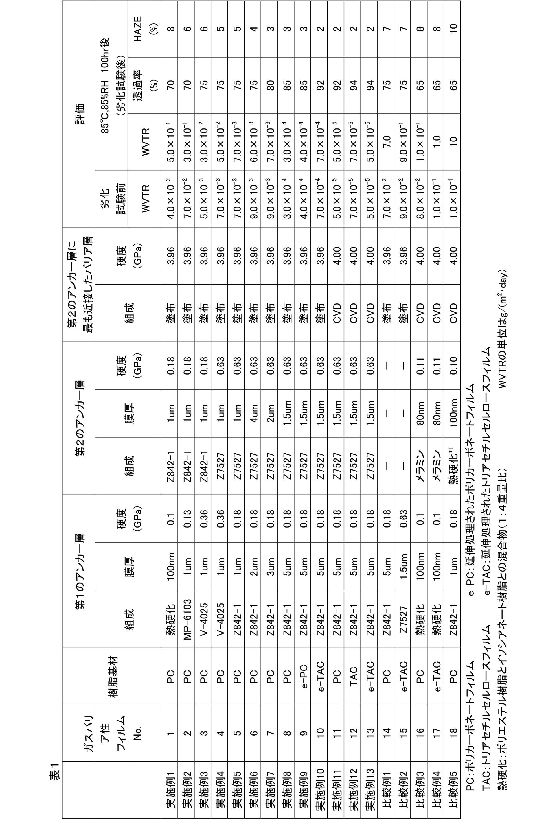
上記表1から明らかなように、本発明のガスバリア性フィルム(実施例1~13)は、優れた水蒸気バリア性、および優れた保存安定性を有することがわかった。
なお、本出願は、2013年2月18日に出願された日本特許出願第2013-029075号に基づいており、その開示内容は、参照により全体として本開示に引用される。
1 ガスバリア性フィルム、
2 アンカー層形成済基材、
3 バリア層、
31 製造装置、
32 送り出しローラー、
33、34、35、36 搬送ローラー、
39、40 成膜ローラー、
41 ガス供給管、
42 プラズマ発生用電源、
43、44 磁場発生装置、
45 巻取りローラー。
2 アンカー層形成済基材、
3 バリア層、
31 製造装置、
32 送り出しローラー、
33、34、35、36 搬送ローラー、
39、40 成膜ローラー、
41 ガス供給管、
42 プラズマ発生用電源、
43、44 磁場発生装置、
45 巻取りローラー。
Claims (9)
- 樹脂基材、
硬化性樹脂を含む第1のアンカー層、
活性エネルギー線硬化性樹脂を含み、かつナノインデンテーション法で測定される表面硬度が前記第1のアンカー層とは異なる第2のアンカー層、および
無機化合物を含むバリア層、
をこの順で含む、ガスバリア性フィルム。 - 前記第1のアンカー層に含まれる前記硬化性樹脂は、活性エネルギー線硬化性樹脂である、請求項1に記載のガスバリア性フィルム。
- ナノインデンテーション法で測定される前記第1のアンカー層の表面硬度をSHa(単位GPa)、ナノインデンテーション法で測定される前記第2のアンカー層の表面硬度をSHb(単位GPa)、およびナノインデンテーション法で測定される前記バリア層の表面硬度をSHc(単位GPa)とした場合、SHa<SHb<SHcの関係である、請求項1または2に記載のガスバリア性フィルム。
- 前記SHa、前記SHb、および前記SHcが、下記数式aおよび下記数式bの関係をともに満たす、請求項3に記載のガスバリア性フィルム。

- 前記第1のアンカー層の膜厚よりも前記第2のアンカー層の膜厚が小さい、請求項1~4のいずれか1項に記載のガスバリア性フィルム。
- 前記樹脂基材はトリアセチルセルロースフィルムである、請求項1~5のいずれか1項に記載のガスバリア性フィルム。
- 前記トリアセチルセルロースフィルムは延伸処理されたトリアセチルセルロースフィルムである、請求項5に記載のガスバリア性フィルム。
- 前記バリア層が、真空成膜法により形成される層と、ポリシラザンを含む層を改質処理して形成される層と、を含む、請求項1~7のいずれか1項に記載のガスバリア性フィルム。
- 請求項1~8のいずれか1項に記載のガスバリア性フィルムを有する、電子デバイス。
Priority Applications (1)
| Application Number | Priority Date | Filing Date | Title |
|---|---|---|---|
| JP2015500166A JPWO2014125877A1 (ja) | 2013-02-18 | 2014-01-20 | ガスバリア性フィルム |
Applications Claiming Priority (2)
| Application Number | Priority Date | Filing Date | Title |
|---|---|---|---|
| JP2013-029075 | 2013-02-18 | ||
| JP2013029075 | 2013-02-18 |
Publications (1)
| Publication Number | Publication Date |
|---|---|
| WO2014125877A1 true WO2014125877A1 (ja) | 2014-08-21 |
Family
ID=51353887
Family Applications (1)
| Application Number | Title | Priority Date | Filing Date |
|---|---|---|---|
| PCT/JP2014/050993 Ceased WO2014125877A1 (ja) | 2013-02-18 | 2014-01-20 | ガスバリア性フィルム |
Country Status (2)
| Country | Link |
|---|---|
| JP (1) | JPWO2014125877A1 (ja) |
| WO (1) | WO2014125877A1 (ja) |
Cited By (3)
| Publication number | Priority date | Publication date | Assignee | Title |
|---|---|---|---|---|
| WO2016043141A1 (ja) * | 2014-09-16 | 2016-03-24 | コニカミノルタ株式会社 | ガスバリア性フィルム |
| WO2016097705A3 (en) * | 2014-12-19 | 2017-07-27 | Fujifilm Manufacturing Europe Bv | Transparent sheet materials |
| US20230002131A1 (en) * | 2019-09-11 | 2023-01-05 | Dai Nippon Printing Co., Ltd. | Barrier film and packaging material |
Citations (7)
| Publication number | Priority date | Publication date | Assignee | Title |
|---|---|---|---|---|
| JPH0970917A (ja) * | 1995-09-07 | 1997-03-18 | Oike Ind Co Ltd | 透明ガスバリア性積層体 |
| JPH11171937A (ja) * | 1997-12-12 | 1999-06-29 | Jsr Corp | 液状硬化性樹脂組成物 |
| JP2000229383A (ja) * | 1999-02-09 | 2000-08-22 | Asahi Glass Co Ltd | 透明被覆成形品 |
| JP2000229384A (ja) * | 1999-02-12 | 2000-08-22 | Asahi Glass Co Ltd | 透明被覆成形品 |
| JP2002137323A (ja) * | 2000-11-06 | 2002-05-14 | Mitsubishi Chemicals Corp | 帯電防止性ガスバリアフィルム |
| JP2011143577A (ja) * | 2010-01-13 | 2011-07-28 | Konica Minolta Holdings Inc | ガスバリアフィルムの製造方法、ガスバリアフィルム及び有機光電変換素子 |
| JP2012016854A (ja) * | 2010-07-07 | 2012-01-26 | Konica Minolta Holdings Inc | ガスバリア性フィルム、及び有機光電変換素子、有機エレクトロルミネッセンス素子 |
-
2014
- 2014-01-20 WO PCT/JP2014/050993 patent/WO2014125877A1/ja not_active Ceased
- 2014-01-20 JP JP2015500166A patent/JPWO2014125877A1/ja active Pending
Patent Citations (7)
| Publication number | Priority date | Publication date | Assignee | Title |
|---|---|---|---|---|
| JPH0970917A (ja) * | 1995-09-07 | 1997-03-18 | Oike Ind Co Ltd | 透明ガスバリア性積層体 |
| JPH11171937A (ja) * | 1997-12-12 | 1999-06-29 | Jsr Corp | 液状硬化性樹脂組成物 |
| JP2000229383A (ja) * | 1999-02-09 | 2000-08-22 | Asahi Glass Co Ltd | 透明被覆成形品 |
| JP2000229384A (ja) * | 1999-02-12 | 2000-08-22 | Asahi Glass Co Ltd | 透明被覆成形品 |
| JP2002137323A (ja) * | 2000-11-06 | 2002-05-14 | Mitsubishi Chemicals Corp | 帯電防止性ガスバリアフィルム |
| JP2011143577A (ja) * | 2010-01-13 | 2011-07-28 | Konica Minolta Holdings Inc | ガスバリアフィルムの製造方法、ガスバリアフィルム及び有機光電変換素子 |
| JP2012016854A (ja) * | 2010-07-07 | 2012-01-26 | Konica Minolta Holdings Inc | ガスバリア性フィルム、及び有機光電変換素子、有機エレクトロルミネッセンス素子 |
Cited By (3)
| Publication number | Priority date | Publication date | Assignee | Title |
|---|---|---|---|---|
| WO2016043141A1 (ja) * | 2014-09-16 | 2016-03-24 | コニカミノルタ株式会社 | ガスバリア性フィルム |
| WO2016097705A3 (en) * | 2014-12-19 | 2017-07-27 | Fujifilm Manufacturing Europe Bv | Transparent sheet materials |
| US20230002131A1 (en) * | 2019-09-11 | 2023-01-05 | Dai Nippon Printing Co., Ltd. | Barrier film and packaging material |
Also Published As
| Publication number | Publication date |
|---|---|
| JPWO2014125877A1 (ja) | 2017-02-02 |
Similar Documents
| Publication | Publication Date | Title |
|---|---|---|
| CN104903090B (zh) | 气体阻隔性膜 | |
| JP5983454B2 (ja) | ガスバリア性フィルム | |
| JP2011143550A (ja) | ガスバリアフィルム | |
| JP7287284B2 (ja) | ガスバリア性フィルム及びその製造方法 | |
| JP7580823B2 (ja) | 光拡散性バリアフィルム | |
| WO2014178332A1 (ja) | ガスバリア性フィルムおよびその製造方法 | |
| WO2016043141A1 (ja) | ガスバリア性フィルム | |
| JP6617701B2 (ja) | ガスバリアーフィルム及びその作製方法 | |
| JP2016155352A (ja) | ガスバリア性フィルムの製造方法及びガスバリア性フィルム | |
| WO2014125877A1 (ja) | ガスバリア性フィルム | |
| JPWO2014103756A1 (ja) | ガスバリア性フィルム | |
| JP2014141055A (ja) | ガスバリア性フィルム | |
| WO2015115510A1 (ja) | ガスバリアー性フィルム及びその製造方法 | |
| WO2014097997A1 (ja) | 電子デバイス | |
| JP6354302B2 (ja) | ガスバリア性フィルム | |
| CN110225823A (zh) | 功能性膜层叠体及电子器件的制造方法 | |
| JP5895855B2 (ja) | ガスバリア性フィルムの製造方法 | |
| WO2015190572A1 (ja) | ガスバリアフィルム積層体とそれを用いた電子部品 | |
| JP6683836B2 (ja) | ガスバリアフィルムおよびガスバリアフィルムの製造方法 | |
| WO2015029732A1 (ja) | ガスバリアフィルムおよびガスバリアフィルムの製造方法 | |
| WO2015133620A1 (ja) | ガスバリア性フィルム | |
| JPWO2015053189A1 (ja) | ガスバリアーフィルム及びその製造方法 | |
| WO2015137389A1 (ja) | ガスバリアーフィルムの製造方法 | |
| WO2015033850A1 (ja) | ガスバリアフィルム積層体とそれを用いた電子部品 | |
| JP2015168238A (ja) | 複合積層フィルムの製造方法 |
Legal Events
| Date | Code | Title | Description |
|---|---|---|---|
| 121 | Ep: the epo has been informed by wipo that ep was designated in this application |
Ref document number: 14751301 Country of ref document: EP Kind code of ref document: A1 |
|
| ENP | Entry into the national phase |
Ref document number: 2015500166 Country of ref document: JP Kind code of ref document: A |
|
| NENP | Non-entry into the national phase |
Ref country code: DE |
|
| 122 | Ep: pct application non-entry in european phase |
Ref document number: 14751301 Country of ref document: EP Kind code of ref document: A1 |