WO2014122853A1 - 受電装置、送電装置および電力伝送システム - Google Patents
受電装置、送電装置および電力伝送システム Download PDFInfo
- Publication number
- WO2014122853A1 WO2014122853A1 PCT/JP2013/083286 JP2013083286W WO2014122853A1 WO 2014122853 A1 WO2014122853 A1 WO 2014122853A1 JP 2013083286 W JP2013083286 W JP 2013083286W WO 2014122853 A1 WO2014122853 A1 WO 2014122853A1
- Authority
- WO
- WIPO (PCT)
- Prior art keywords
- field coupling
- voltage
- wound body
- power transmission
- power
- Prior art date
- Legal status (The legal status is an assumption and is not a legal conclusion. Google has not performed a legal analysis and makes no representation as to the accuracy of the status listed.)
- Ceased
Links
Images












Classifications
-
- H—ELECTRICITY
- H02—GENERATION; CONVERSION OR DISTRIBUTION OF ELECTRIC POWER
- H02J—ELECTRIC POWER NETWORKS; CIRCUIT ARRANGEMENTS OR SYSTEMS FOR SUPPLYING OR DISTRIBUTING ELECTRIC POWER; SYSTEMS FOR STORING ELECTRIC ENERGY
- H02J50/00—Circuit arrangements or systems for wireless supply or distribution of electric power
- H02J50/10—Circuit arrangements or systems for wireless supply or distribution of electric power using inductive coupling
- H02J50/12—Circuit arrangements or systems for wireless supply or distribution of electric power using inductive coupling of the resonant type
-
- H—ELECTRICITY
- H02—GENERATION; CONVERSION OR DISTRIBUTION OF ELECTRIC POWER
- H02J—ELECTRIC POWER NETWORKS; CIRCUIT ARRANGEMENTS OR SYSTEMS FOR SUPPLYING OR DISTRIBUTING ELECTRIC POWER; SYSTEMS FOR STORING ELECTRIC ENERGY
- H02J50/00—Circuit arrangements or systems for wireless supply or distribution of electric power
- H02J50/05—Circuit arrangements or systems for wireless supply or distribution of electric power using capacitive coupling
-
- H—ELECTRICITY
- H02—GENERATION; CONVERSION OR DISTRIBUTION OF ELECTRIC POWER
- H02J—ELECTRIC POWER NETWORKS; CIRCUIT ARRANGEMENTS OR SYSTEMS FOR SUPPLYING OR DISTRIBUTING ELECTRIC POWER; SYSTEMS FOR STORING ELECTRIC ENERGY
- H02J50/00—Circuit arrangements or systems for wireless supply or distribution of electric power
- H02J50/40—Circuit arrangements or systems for wireless supply or distribution of electric power using two or more transmitting or receiving devices
-
- H—ELECTRICITY
- H02—GENERATION; CONVERSION OR DISTRIBUTION OF ELECTRIC POWER
- H02J—ELECTRIC POWER NETWORKS; CIRCUIT ARRANGEMENTS OR SYSTEMS FOR SUPPLYING OR DISTRIBUTING ELECTRIC POWER; SYSTEMS FOR STORING ELECTRIC ENERGY
- H02J50/00—Circuit arrangements or systems for wireless supply or distribution of electric power
- H02J50/80—Circuit arrangements or systems for wireless supply or distribution of electric power involving the exchange of data, concerning supply or distribution of electric power, between transmitting devices and receiving devices
-
- H—ELECTRICITY
- H02—GENERATION; CONVERSION OR DISTRIBUTION OF ELECTRIC POWER
- H02J—ELECTRIC POWER NETWORKS; CIRCUIT ARRANGEMENTS OR SYSTEMS FOR SUPPLYING OR DISTRIBUTING ELECTRIC POWER; SYSTEMS FOR STORING ELECTRIC ENERGY
- H02J50/00—Circuit arrangements or systems for wireless supply or distribution of electric power
- H02J50/70—Circuit arrangements or systems for wireless supply or distribution of electric power involving the reduction of electric, magnetic or electromagnetic leakage fields
-
- H—ELECTRICITY
- H02—GENERATION; CONVERSION OR DISTRIBUTION OF ELECTRIC POWER
- H02J—ELECTRIC POWER NETWORKS; CIRCUIT ARRANGEMENTS OR SYSTEMS FOR SUPPLYING OR DISTRIBUTING ELECTRIC POWER; SYSTEMS FOR STORING ELECTRIC ENERGY
- H02J7/00—Circuit arrangements for charging or discharging batteries or for supplying loads from batteries
- H02J7/40—Circuit arrangements for charging or discharging batteries or for supplying loads from batteries characterised by the exchange of charge or discharge related data
- H02J7/42—Circuit arrangements for charging or discharging batteries or for supplying loads from batteries characterised by the exchange of charge or discharge related data with electronic devices having internal batteries, e.g. mobile phones
Definitions
- the present invention relates to a power reception device, a power transmission device, and a power transmission system, and particularly to a power reception device, a power transmission device, and a power transmission system corresponding to the electric field coupling method.
- Patent Document 1 An example of an apparatus that transmits electric power by an electric field coupling method is disclosed in Patent Document 1.
- This device is composed of an energy generating device and a consuming device located at a short distance from each other.
- the device is also modeled in the form of an interaction between asymmetric oscillating electric dipoles, which consists of a high-voltage high-frequency generator or a high-voltage high-frequency charge placed between two electrodes. These dipoles exert mutual influence on each other. Electrical energy and / or information is transported remotely using a Coulomb field surrounding any collection of charged conductors in a slowly changing variable state.
- Patent Document 2 an example of a system that performs power transmission by a magnetic field coupling method is disclosed in Patent Document 2.
- This system is formed by a master unit having a power transmission unit and a slave unit having a power reception unit.
- the power transmission unit transmits power through an alternating magnetic field based on the output of the power source, and the power reception unit receives the power by converting the alternating magnetic field coming from the outside into an electric quantity.
- a main object of the present invention is to provide a power receiving device, a power transmitting device, and a power transmission system that can cope with both the magnetic field coupling method and the electric field coupling method while suppressing the complexity of the circuit configuration.
- a power receiving device (20: reference numeral corresponding to the embodiment; the same applies hereinafter) according to the present invention receives power transmitted from a power transmitting device (10a, 10b) employing at least one of an electric field coupling method and a magnetic field coupling method.
- the first connecting means is connected to the primary coil (L5) having one end and the other end respectively connected to one end and the plate-like body of the wound body, and to the one input end and the other input end, respectively.
- the second connection means includes a secondary coil (L6) having one end and the other end and forming a step-down transformer (22) together with the primary coil, and the second connection means connects the first end of the wound body to the one input end
- a conductive line (SL1) and a second conductive line (SL2) that connects the other end of the wound body to the other input end are included.
- a first capacitor (C1) provided on the first conductive line is further provided.
- a second capacitor (C2) provided between the first conductive line and the second conductive line is further provided.
- the first switching means (SW1) for switching the connection destination of one end of the wound body between the one end of the primary coil and the first conductive wire, and the connection destination of the other input end of the secondary coil Second switching means (SW2) for switching between the other end and the second conductive line is further provided.
- the conversion means includes a first voltage conversion means (32) corresponding to the electric field coupling method and a second voltage conversion means (30) corresponding to the magnetic field coupling method, while the input end is the first voltage conversion means (32).
- Including a first other voltage input terminal (T322) assigned to the second voltage conversion means and a second other voltage input terminal (T302) assigned to the second voltage conversion means. 1 is connected to one voltage input terminal and the first other voltage input terminal, respectively, and the first conductive line and the second conductive line are respectively connected to the second one voltage input terminal and the second other voltage input terminal.
- a third switching means (SW3) for switching the connection destination of one end of the wound body between the one end of the primary coil and the first conductive wire, and a fourth switching means for intermittently connecting the second conductive wire ( SW4) is further provided.
- the plate-like body includes a plurality of partial plate-like bodies (E3_1, E3_2).
- a power transmission device (40) is a power transmission device that transmits power to a power receiving device (50a, 50b) that employs at least one of an electric field coupling method and a magnetic field coupling method, and has a conductive wound body (L9).
- a conductive plate-like body (E4, E4_1, E4_2), one output end (T421) to which an AC voltage is applied and the other output end (T422), and a conversion means for converting a DC voltage into an AC voltage (42)
- first connection means (44) for electrically connecting one end and a plate-like body of the wound body to one output end and the other output end during electric field coupling, and one end of the wound body during magnetic field coupling;
- Second connection means (SL3, SL4) for electrically connecting the other end to the one output end and the other output end is provided.
- the first connecting means is connected to the primary coil (L7) having one end and the other end connected to the one output end and the other output end, respectively, and to the one end and the plate-like body of the wound body.
- a secondary coil (L8) having one end and the other end and forming a step-up transformer (44) together with the primary coil, and the second connection means connects the one end of the wound body to the one output end.
- One conductive line (SL3) and a second conductive line (SL4) connecting the other end of the wound body to the other output end are included.
- a first capacitor (C4) provided on the first conductive line is further provided.
- a second capacitor (C5) provided between the first conductive line and the second conductive line is further provided.
- the first switching means (SW5) for switching the connection destination of one end of the wound body between the one end of the secondary coil and the first conductive line, and the connection destination of the other output end of the primary coil Second switching means (SW6) for switching between the other end and the second conductive line is further provided.
- a power transmission system includes a power transmission device (10a, 10b) that employs at least one of an electric field coupling method and a magnetic field coupling method, and a power reception device (20) that receives power transmitted from the power transmission device.
- the power receiving device includes a conductive winding body (L4), conductive plate bodies (E3, E3_1, E3_2), and one input terminal to which an AC voltage is applied (T241, T301, T321).
- T242, T302, T322 And other input ends (T242, T302, T322), conversion means (24, 30, 32) for converting AC voltage to DC voltage, one end of the wound body and plate-like body at one input end during electric field coupling And a first connection means (22) for electrically connecting to the other input end, and a second connection means for electrically connecting one end and the other end of the wound body to the one input end and the other input end during magnetic field coupling ( SL1, SL2).
- a power transmission system is a power transmission system including a power receiving device (50a, 50b) that employs at least one of an electric field coupling method and a magnetic field coupling method, and a power transmission device (40) that transmits power to the power receiving device.
- the power transmission device has a conductive winding body (L9), conductive plate bodies (E4, E4_1, E4_2), one output end (T421) and the other output end (T422) to which an AC voltage is applied.
- the wound body functions as one electrode for power reception or power transmission during power reception or power transmission according to the electric field coupling method, and also functions as an electromagnetic induction coil during power reception or power transmission according to the magnetic field coupling method.
- the plate-like body functions as the other electrode for power reception or power transmission during power reception or power transmission according to the electric field coupling method.
- (A) is a block diagram which shows an example of the power transmission apparatus which comprises an electric power transmission system
- (B) is a block diagram which shows another example of the electric power transmission apparatus which comprises an electric power transmission system. It is a block diagram which shows an example of the power receiving apparatus which comprises an electric power transmission system.
- (A) is an illustration figure which shows an example of the connection aspect of the switch at the time of electric field coupling
- (B) is an illustration figure which shows an example of the connection aspect of the switch at the time of magnetic field coupling. It is a flowchart which shows a part of operation
- (A) is an illustration figure which shows an example of the state which looked at the housing
- (B) is an illustration figure which shows another example of the state which looked at the housing
- (C) is an illustrative view showing another example of a state in which the casing forming the power receiving device is viewed from above
- (D) is still another example of the state in which the casing forming the power receiving device is viewed from above.
- (E) is an illustrative view showing another example of a state in which the casing forming the power receiving device is viewed from above
- (F) is a state in which the casing forming the power receiving device is viewed from above.
- FIG. It is an illustration figure which shows another example of these. It is a block diagram which shows a part of other example of the power receiving apparatus which comprises an electric power transmission system. It is a block diagram which shows a part of other example of the power receiving apparatus which comprises an electric power transmission system. It is a block diagram which shows a part of further another example of the power receiving apparatus which comprises an electric power transmission system.
- (A) is an illustration figure which shows another example of the state which looked at the housing
- B) shows another example of the state which looked at the housing
- FIG. It is a block diagram which shows another example of the power receiving apparatus which comprises an electric power transmission system.
- FIG. 1 It is a block diagram which shows an example of the power transmission apparatus which comprises an electric power transmission system.
- A is a block diagram showing an example of a power receiving device constituting the power transmission system
- B is a block diagram showing another example of the power receiving device constituting the power transmission system.
- A) is an illustration figure which shows an example of the connection aspect of the switch at the time of electric field coupling
- (B) is an illustration figure which shows an example of the connection aspect of the switch at the time of magnetic field coupling.
- FIG. 1 It is a block diagram which shows a part of other example of the power transmission apparatus which comprises an electric power transmission system. It is a block diagram which shows a part of other example of the power transmission apparatus which comprises an electric power transmission system. It is a block diagram which shows another example of the power transmission apparatus which comprises an electric power transmission system.
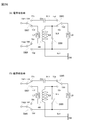
- (A) is an illustration figure which shows an example of the connection aspect of the switch at the time of electric field coupling
- (B) is an illustration figure which shows an example of the connection aspect of the switch at the time of magnetic field coupling.
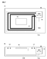
- (A) is an illustration figure which shows an example of the state which looked at the housing
- (B) is an illustration figure which shows an example of the state which looked at the housing
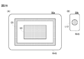
- (A) is an illustration figure which shows an example of the state which looked at the housing
- (B) is the housing
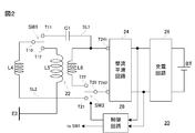
- the power transmission system of this embodiment is formed by the power transmission device 10a shown in FIG. 1 (A) or the power transmission device 10b shown in FIG. 1 (B) and the power reception device 20 shown in FIG.
- a power transmission device 10a illustrated in FIG. 1A corresponds to an electric field coupling method
- a power transmission device 10b illustrated in FIG. 1B corresponds to a magnetic field coupling method.
- the power receiving device 20 shown in FIG. 2 corresponds to both the electric field coupling method and the magnetic field coupling method.
- the inverter 12 converts the DC voltage output from the DC power supply Vcc into an AC voltage.
- the converted AC voltage is applied to the primary coil L1 that forms the step-up transformer 14.
- the secondary coil L2 has a larger number of turns than the number of turns of the primary coil L1, and forms the step-up transformer 14 together with the primary coil L1.
- the one end and the other end of the secondary coil L2 are connected to the electric field coupling electrodes E1 and E2, respectively.
- the AC voltage boosted by the step-up transformer 14 is applied to the electrodes E1 and E2.
- the DC voltage output from the DC power source Vcc is converted into an AC voltage by the inverter 12.
- the converted AC voltage is applied to the electromagnetic induction coil L3 for magnetic field coupling.
- switch SW1 has a common terminal T10 and branch terminals T11 and T12
- switch SW2 has a common terminal T20 and branch terminals T21 and T22.
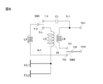
- One end and the other end of wound body L4 are connected to common terminal T10 of switch SW1 and branch terminal T21 of switch SW2, respectively.
- the branch terminal T12 and the plate-like electrode E3 of the switch SW1 are connected to one end and the other end of the primary coil L5 that form the step-down transformer L5 together with the secondary coil L6.
- the secondary coil L6 has a smaller number of turns than the number of turns of the primary coil L5.
- One end of the secondary coil L6 is connected to one input terminal T241 provided in the rectifying and smoothing circuit 24, and the other end of the secondary coil L6 is connected to the branch terminal T22 of the switch SW2.
- a common terminal T20 of the switch SW2 is connected to the other input terminal T242 provided in the rectifying / smoothing circuit 24.
- One input terminal T241 of the rectifying / smoothing circuit 24 is also connected to the branch terminal T11 of the switch SW1 via the capacitor C1.
- the conductive wire connecting the branch terminal T12 and the one input end T241 of the rectifying / smoothing circuit 24 is particularly defined as “SL1”, and the other end of the wound body L4 is connected to the branch terminal T21 of the switch SW2.
- the conductive line to be defined is particularly defined as “SL2”.
- the capacitor C1 forms an LC resonance circuit together with the wound body L4, and the resonance frequency of the LC resonance circuit is adjusted to be close to the frequency of the AC voltage generated by the inverter 12.
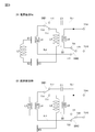
- common terminal T10 of switch SW1 is connected to branch terminal T11, and common terminal T20 of switch SW2 is connected to branch terminal T21.
- One end of wound body L4 is connected to one end of primary coil L5 forming step-down transformer 22, and the other end of wound body L4 is opened. Further, the other end of the secondary coil L6 constituting the step-down transformer 22 is connected to the other input end T242 of the rectifying and smoothing circuit 24. At this time, the wound body L4 functions as an electric field coupling electrode.
- the wound body L4 and the electrode E3 are electrically coupled to the electrodes E1 and E2.
- an AC voltage having the same frequency as the AC voltage applied to the electrodes E1 and E2 is excited in the wound body L4 and the electrode E3.
- the excited AC voltage is applied to one input terminal T241 and the other input terminal T242 of the rectifying and smoothing circuit 24 through the step-down transformer 22.
- common terminal T10 of switch SW1 is connected to branch terminal T12
- common terminal T20 of switch SW2 is connected to branch terminal T22.
- One end of the wound body L4 is connected to one input terminal T241 of the rectifying / smoothing circuit 24 via the switch SW1 and the capacitor C1, and the other end of the wound body L4 is connected to the other input terminal of the rectifying / smoothing circuit 24 via the switch SW2.
- the wound body L4 functions as an electromagnetic induction coil for magnetic field coupling.
- the wound body L4 is magnetically coupled to the electromagnetic induction coil L3.
- an AC voltage having the same frequency as the AC voltage applied to the electromagnetic induction coil L3 is excited in the wound body L4.
- the excited AC voltage is applied to one input terminal T241 and the other input terminal T242 of the rectifying and smoothing circuit 24.
- the rectifying / smoothing circuit 24 rectifies and smoothes the applied AC voltage to generate a DC voltage, and supplies the generated DC voltage to the charging circuit 26.
- the charging circuit 26 charges the battery BT based on the supplied DC voltage.
- the DC voltage generated by the rectifying / smoothing circuit 24 is also supplied to the control circuit 28.
- the control circuit 28 controls the setting of the switches SW1 and SW2 with reference to the supplied DC voltage. Specifically, the control circuit 28 executes processing according to the flowchart shown in FIG.
- step S1 the common terminal T10 of the switch SW1 is connected to the branch terminal T11, and the common terminal T20 of the switch SW2 is connected to the branch terminal T21.
- step S3 the voltage value of the DC voltage supplied from the rectifying / smoothing circuit 24 is detected, and in step S5, it is determined whether or not the detected voltage value is equal to or greater than a specified value.
- step S7 the connection destination of the common terminal T10 provided in the switch SW1 is changed between the branch terminals T11 and T12, and the connection destination of the common terminal T20 provided in the switch SW2 is changed between the branch terminals T21 and T22.
- the process returns to step S3.
- step S5 When the common terminal T10 of the switch SW1 is connected to the branch terminal T11 and the common terminal T20 of the switch SW2 is connected to the branch terminal T21, if the determination result in step S5 indicates YES, the power transmission corresponding to the electric field coupling method is performed. It is assumed that the device 10a has been brought close to the power receiving device 20, and power reception according to the electric field coupling method is started.
- step S5 shows YES
- the magnetic field coupling It is considered that the power transmission device 10b corresponding to the method is brought closer to the power receiving device 20, and power reception according to the magnetic field coupling method is started.
- the specified value in step S5 may be the same value or a different value in the electric field coupling method and the magnetic field coupling method.
- the electric field coupling method and the magnetic field coupling method are switched depending on the voltage value after rectification and smoothing.
- a wireless communication is performed by separately providing a transmission side communication circuit and a reception side communication circuit in the power transmission device and the power reception device, respectively.
- the electromagnetic coupling method and the magnetic field coupling method may be switched.
- the transmission side communication circuit of the electric field coupling type power transmission device transmits the electric field status signal to the reception side communication circuit when receiving the electric field status signal from the reception side communication circuit, and starts transmission when the electric field coupling hold signal is received. Have a function to let you.
- the transmission side communication circuit of the magnetic field coupling type power transmission device transmits the magnetic field status signal to the reception side communication circuit when receiving the magnetic field status signal from the reception side communication circuit, and starts power transmission when the magnetic field coupling hold signal is received. Have a function to let you.
- the power transmitting apparatus 10a corresponding to the electric field coupling method is regarded as being brought closer to the power receiving apparatus 20, and is transmitted to the power transmitting apparatus.
- An electric field coupling hold signal is transmitted, and power reception according to the electric field coupling method is started.
- the communication circuit of the power receiving device sends an electric field status signal to the power transmitting device and times out, the magnetic field status signal is sent, and when the magnetic field status signal is received from the power transmitting device, the power transmission corresponding to the magnetic field coupling method is performed.
- a magnetic field coupling hold signal is transmitted to the power transmitting device, and power reception according to the magnetic field coupling method is started.
- the communication circuit of the receiving apparatus sends a magnetic field status signal and times out, it repeats from where the electric field status signal is sent.
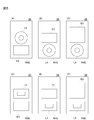
- the wound body L4 and the electrode E3 are provided in the power receiving device 20 in the mode shown in FIG. According to FIG. 5A, the wound body L4 is formed in a disc shape, and the electrode E3 is formed in a rectangular plate shape. Further, the power receiving device 20 has a rectangular parallelepiped housing RHS.
- the wound body L4 is provided in the center of the main surface of the housing RHS in a posture in which the winding axis is orthogonal to the main surface of the housing RHS.
- the electrode E3 is provided at a position on one end side in the length direction of the main surface of the housing RHS so that the orientation of the main surface coincides with the orientation of the main surface of the housing RHS.
- the power transmission device 10a corresponds to the electric field coupling method
- the power transmission device 10b corresponds to the magnetic field coupling method.
- the power receiving device 20 receives the power transmitted from the power transmitting device 10a or 10b.
- the wound body L4 and the electrode E3 are both conductive.
- the rectifying / smoothing circuit 24 has one input terminal T241 and the other input terminal T242 to which an AC voltage is applied, and converts the AC voltage into a DC voltage.
- Step-down transformer 22 electrically connects one end of wound body L4 and electrode E3 to one input end T241 and the other input end T242 during electric field coupling.
- Conductive lines SL1 and SL2 electrically connect one end and the other end of wound body L4 to one input end T241 and the other input end T242 during magnetic field coupling.
- the wound body L4 functions as one electrode for power reception when receiving power according to the electric field coupling method, and also functions as an electromagnetic induction coil when receiving power according to the magnetic field coupling method.
- the electrode E3 functions as the other electrode for receiving power when receiving power according to the electric field coupling method.
- the wound body L4 and the electrode E3 may be provided in the power receiving device 20 in the manner shown in FIGS. 5 (B) to 5 (F).
- the wound body L4 is provided at a position on one end side in the length direction of the main surface of the housing RHS, and the electrode E3 is provided at the center of the main surface of the housing RHS.
- the wound body L4 is provided at a position on one end side in the length direction of the main surface of the housing RHS, and the electrode E3 whose main surface is enlarged is the main surface of the housing RHS. It is provided at a position on the other end side in the length direction from the center of.
- the modes shown in FIGS. 5D to 5F are the same as FIGS. 5A to 5C except that the shape of the main surface of the wound body L4 is rectangular.
- a capacitor C1 is provided on the conductive line SL1.
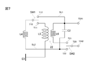
- a capacitor C2 is added between the conductive lines SL1 and SL2 as shown in FIG. 6, a capacitor C2 is provided instead of the capacitor C1 as shown in FIG. 7, and both the capacitors C1 and C2 are omitted. You may do it.
- a single electrode E3 is provided.
- the electrode E3 is divided into partial electrodes E3_1 and E3_2, and the partial electrodes E3_1 and E3_2 are provided on the main surface of the housing RHS in the manner shown in FIG. 9A or 9B. It may be. 9A and 9B, the partial electrode E3_1 is provided on one end side in the length direction of the housing RHS, and the partial electrode E3_2 is provided on the other end side in the length direction of the housing RHS. .
- the wound body L4 is provided at the center of the main surface of the housing RHS in both FIG. 9 (A) and FIG. 9 (B).
- the power transmission device can be placed in either direction (it can be placed in an easy-to-place orientation).
- the power transmission device 10a corresponds only to the electric field coupling method
- the power transmission device 10b corresponds to only the magnetic field coupling method.
- the configurations of the power transmission devices 10a and 10b may be integrated to prepare a power transmission device that supports both the electric field coupling method and the magnetic field coupling method.
- power receiving apparatus 10 of another embodiment is provided with rectifying / smoothing circuits 30 and 32 corresponding to the magnetic field coupling method and the electric field coupling method, respectively, instead of rectifying / smoothing circuit 24 shown in FIG. 2 is the same as the rectifying / smoothing circuit 24 shown in FIG. 2 except that a part of the configuration is modified. Therefore, the overlapping description regarding the same configuration is omitted as much as possible.
- the switch SW3 has a common terminal T40, a branch terminal T41, and T42.
- the rectifying / smoothing circuit 30 has one input end T301 and the other input end T302, and the rectifying / smoothing circuit 32 has one input end T321 and the other input end T322.
- the common terminal T40 is connected to one end of the wound body L4
- the branch terminal T42 is connected to one input end T301 of the rectifying and smoothing circuit 30 via the capacitor C1
- the branch terminal T41 is the primary coil L5 that forms the step-down transformer 22. Is connected to one end.
- the other input end T302 of the rectifying / smoothing circuit 30 is connected to the other end of the wound body L4 via the switch SW4. Further, the one input end T321 and the other input end T322 of the rectifying / smoothing circuit 32 are connected to one end and the other end of the secondary coil L6 forming the step-down transformer 22, respectively.
- the conductive wire connecting the branch terminal T42 and one input end T301 of the rectifying / smoothing circuit 30 is defined as “SL1”, and the other end of the wound body L4 and the other input of the rectifying / smoothing circuit 30 are defined.
- a conductive line connecting the end T302 is defined as “SL2”.
- the rectifying / smoothing circuits 30 and 32 are both configured as shown in FIG. This configuration is also adopted in the rectifying / smoothing circuit 24 shown in FIG.
- the cathode of the diode D1 is connected to the cathode of the diode D2
- the anode of the diode D3 is connected to the anode of the diode D4.
- the anode of diode D1 is connected to the cathode of diode D3, and the anode of diode D2 is connected to the cathode of diode D4.
- One input terminal T301 or T321 is connected to the anode of the diode D1, and the other input terminal T302 or T322 is connected to the anode of the diode D2.
- One end of the capacitor C3 is connected to the cathode of the diode D1, and the other end of the capacitor C3 is connected to the anode of the diode D3.
- One end and the other end of the capacitor C3 are connected to one input end and the other input end of the charging circuit 26, respectively.
- the AC voltage applied to one input terminal T301 (T321) and the other input terminal T302 (T322) is full-wave rectified by the diodes D1 to D4, and the rectified voltage is smoothed by the capacitor C3.
- the AC voltage is thus converted into a DC voltage, and the converted DC voltage is supplied to the charging circuit 26.
- the entire circuit can be simplified by sharing the rectifying and smoothing circuit as shown in FIG. 2, it is optimal for downsizing the entire apparatus.
- one end of the secondary coil L6 is connected during magnetic field coupling, and in some cases, unnecessary resonance is generated by the secondary coil L6 and the parasitic capacitance generated mainly by the switch SW2. It becomes. In that case, it is effective to use a circuit configuration as shown in FIG.
- the wound body L4 and the electrode E3 are electrically coupled to the electrodes E1 and E2.
- an AC voltage having the same frequency as the AC voltage applied to the electrodes E1 and E2 is excited in the wound body L4 and the electrode E3.
- the excited AC voltage is applied to one input terminal T321 and the other input terminal T322 of the rectifying and smoothing circuit 32 through the step-down transformer 22.
- common terminal T30 of switch SW3 is connected to branch terminal T32, and switch SW4 is turned on.
- One end of the wound body L4 is connected to one input end T301 of the rectifying and smoothing circuit 30 via the switch SW3 and the capacitor C1.
- the other end of the wound body L4 is connected to the other input end T302 of the rectifying / smoothing circuit 30 via the switch SW4.
- the wound body L4 functions as an electromagnetic induction coil for magnetic field coupling.
- the wound body L4 is magnetically coupled to the electromagnetic induction coil L3.
- an AC voltage having the same frequency as the AC voltage applied to the electromagnetic induction coil L3 is excited in the wound body L4.
- the excited AC voltage is applied to one input terminal T301 and the other input terminal T302 of the rectifying and smoothing circuit 30.
- control circuit 28 refers to the DC voltage supplied from the rectifying / smoothing circuit 30 or 32 to control the setting of the switches SW3 and SW4. Specifically, the control circuit 28 executes processing according to the flowchart shown in FIG.
- step S11 the common terminal T30 of the switch SW3 is connected to the branch terminal T31, and the switch SW4 is turned off.
- step S13 the voltage value of the DC voltage supplied from the rectifying / smoothing circuit 30 or 32 is detected, and in step S15, it is determined whether or not the detected voltage value is equal to or greater than a specified value.
- step S17 If the determination result is NO, the connection of the switches SW3 and SW4 is changed in step S17.
- the connection destination of the common terminal T30 provided in the switch SW3 is changed between the branch terminals T31 and T32, and the switch SW4 is changed between the off state and the on state.
- the process returns to step S13.
- the power receiving device 20 is changed to the electric field coupling method. It is assumed that the corresponding power transmission device 10a has been approached, and power reception according to the electric field coupling method is started.
- the specified value in step S15 may be the same value or a different value in the electric field coupling method and the magnetic field coupling method.
- the electric field coupling method and the magnetic field coupling method are switched depending on the voltage value after rectification and smoothing.
- a wireless communication is performed by separately providing a transmission side communication circuit and a reception side communication circuit in the power transmission device and the power reception device, respectively.
- the electromagnetic coupling method and the magnetic field coupling method may be switched.
- the wound body L4 functions as one electrode for power reception when receiving power according to the electric field coupling method, and also functions as an electromagnetic induction coil when receiving power according to the magnetic field coupling method.
- the electrode E3 functions as the other electrode for receiving power when receiving power according to the electric field coupling method.
- a capacitor C1 is provided on the conductive line SL1.
- a capacitor C2 is added between the conductive lines SL1 and SL2 as shown in FIG. 15, a capacitor C2 is provided instead of the capacitor C1 as shown in FIG. 16, and both the capacitors C1 and C2 are omitted. You may do it.
- a single electrode E3 is provided. However, as shown in FIG. 17, the electrode E3 may be divided into partial electrodes E3_1 and E3_2.
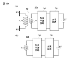
- a power transmission system of another embodiment is formed by the power transmission device 40 shown in FIG. 18 and the power reception device 50a shown in FIG. 19A or the power reception device 50b shown in FIG. 19B.
- the power transmission device 40 illustrated in FIG. 18 corresponds to both the electric field coupling method and the magnetic field coupling method.
- the power receiving device 50a illustrated in FIG. 19A corresponds only to the electric field coupling method
- the power receiving device 50b illustrated in FIG. 19B corresponds to only the magnetic field coupling method.
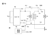
- the inverter 42 has one output terminal T421 and the other output terminal T422, and converts the DC voltage output from the DC power supply Vcc into an AC voltage.
- the switch SW5 has a common terminal T50 and branch terminals T51 and T52, and the switch SW6 has a common terminal T60 and branch terminals T61 and T62.
- One output terminal T421 of the inverter 42 is connected to one terminal of the primary coil L7 constituting the step-up transformer 44, the other terminal of the primary coil L7 is connected to the branch terminal T61 of the switch SW6, and the common terminal T60 of the switch SW6 is an inverter. 42 is connected to the other output terminal T422.
- One output terminal T421 of the inverter 42 is also connected to the branch terminal T52 of the switch SW5 via the capacitor C4.
- the common terminal T50 of the switch SW5 is connected to one end of the wound body L9, and the other end of the wound body L9 is connected to the branch terminal T62 of the switch SW6.
- the branch terminal T51 of the switch SW5 is connected to one end of the secondary coil L8 constituting the step-up transformer 44, and the other end of the secondary coil L8 is connected to the plate-like electrode E4.
- the secondary coil L8 has a larger number of turns than the number of turns of the primary coil L7.
- the conductive wire connecting one output terminal T421 of the inverter 42 and the branch terminal T52 of the switch SW5 is particularly defined as “SL3”, and the branch terminal T62 of the switch SW6 and the other end of the wound body L9 are connected to each other.
- the conductive line to be connected is particularly defined as “SL4”.
- the capacitor C4 forms an LC resonance circuit together with the wound body L9, and the resonance frequency of the LC resonance circuit is adjusted to be close to the frequency of the AC voltage generated by the inverter 42.
- power receiving circuit 50a has electrodes E5 and E6 for electric field coupling. Electrodes E5 and E6 are respectively connected to one end and the other end of primary coil L10 constituting step-down transformer 52.
- the secondary coil L11 constituting the step-down transformer 52 has a number of turns smaller than that of the primary coil, and one end and the other end of the secondary coil L11 are connected to one input end and the other input end of the rectifying / smoothing circuit 54, respectively.
- the A charging circuit 56 for charging the battery BT is provided at the subsequent stage of the rectifying / smoothing circuit 54.
- power reception circuit 50b has electromagnetic induction coil L12 for magnetic field coupling.
- One end and the other end of the electromagnetic induction coil L12 are connected to one input end and the other input end of the rectifying and smoothing circuit 54, respectively.
- a charging circuit 56 that charges the battery BT is also provided after the rectifying / smoothing circuit 54.
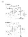
- common terminal T50 of switch SW5 is connected to branch terminal T51, and common terminal T60 of switch SW6 is connected to branch terminal T61.
- One end of the wound body L9 is connected to one end of the secondary coil L8 that forms the step-up transformer 44, and the other end of the wound body L9 is opened. Further, the other end of the primary coil L7 constituting the step-up transformer 44 is connected to the other output end T422 of the inverter 42. At this time, the wound body L9 functions as an electric field coupling electrode.
- the AC voltage output from one output terminal T421 and the other output terminal T422 of the inverter 42 is boosted by the step-up transformer 44 and then applied to the wound body L9 and the electrode E4.
- the wound body L9 and the electrode E4 are electrically coupled to the electrodes E5 and E6.
- An alternating voltage having the same frequency as the alternating voltage applied to the wound body L9 and the electrode E4 is excited on the electrodes E5 and E6.
- the excited AC voltage is stepped down by the step-down transformer 52 and then converted into a DC voltage by the rectifying and smoothing circuit 54.
- the charging circuit 56 charges the battery BT based on the DC voltage thus converted.
- common terminal T50 of switch SW5 is connected to branch terminal T52, and common terminal T60 of switch SW6 is connected to branch terminal T62.
- One end of wound body L9 is connected to one output end T421 of inverter 42 via switch SW5 and capacitor C4.
- the other end of the wound body L9 is connected to the other output terminal T422 of the inverter via the switch SW6.
- the wound body L9 functions as an electromagnetic induction coil for magnetic field coupling.
- the alternating voltage output from one output end T421 and the other output end T422 of the inverter 42 is applied to one end and the other end of the wound body L9.
- the wound body L9 is magnetically coupled to the electromagnetic induction coil L12.
- an AC voltage having the same frequency as the AC voltage applied to the wound body L9 is excited in the electromagnetic induction coil L12.
- the rectifying and smoothing circuit 54 converts the excited AC voltage into a DC voltage
- the charging circuit 56 charges the battery BT based on the converted DC voltage.
- control circuit 46 refers to the impedance on the output side of the inverter 42 to control the settings of the switches SW5 and SW6. Specifically, the control circuit 46 executes processing according to the flowchart shown in FIG.
- step S21 the common terminal T50 of the switch SW5 is connected to the branch terminal T51, and the common terminal T60 of the switch SW6 is connected to the branch terminal T61.
- step S23 the impedance on the output side of the inverter 42 is measured, and in step S25, it is determined whether or not the measured impedance is within a specified range. If the determination result is NO, it is assumed that neither the power receiving device 50a nor 50b exists in the vicinity of the power transmitting device 40, and the process returns to step S23.
- step S25 determines whether one of the power receiving devices 50a and 50b exists in the vicinity of the power transmitting device 50, and which of the power receiving devices 50a and 50b exists in step S27. And in S29. In both steps S27 and S29, the impedance measured in step S23 is referred to.
- step S27 power transmission is started with the common terminal T50 of the switch SW5 connected to the branch terminal T51 and the common terminal T60 of the switch SW6 connected to the branch terminal T61.
- step S29 If the impedance is different from both the value corresponding to the electric field coupling method and the value corresponding to the magnetic field coupling method, NO is determined in step S29, and the connection of the switches SW5 and SW6 is changed in step S31.
- the connection destination of the common terminal T50 provided in the switch SW5 is changed between the branch terminals T51 and T52, and the connection destination of the common terminal T60 provided in the switch SW6 is changed between the branch terminals T61 and T62.
- the process returns to step S23.
- step S23 If the impedance measured in step S23 shows a value corresponding to the magnetic field coupling method, it is considered that the power receiving device 50b exists in the vicinity of the power transmitting device 50, and YES is determined in step S25 and step S29. As a result, power transmission is started with the common terminal T50 of the switch SW5 connected to the branch terminal T52 and the common terminal T60 of the switch SW6 connected to the branch terminal T62.
- the specified range in step S25 may be the same range or a different range in the electric field coupling method and the magnetic field coupling method.
- the electric field coupling method and the magnetic field coupling method are switched depending on the impedance value, but by separately providing a transmission side communication circuit and a reception side communication circuit in the power transmission device and the power reception device, and performing wireless communication, The electromagnetic coupling method and the magnetic field coupling method may be switched.
- the transmission side communication circuit of the power transmission apparatus transmits the electric field status signal to the reception side communication circuit when receiving the electric field status signal from the reception side communication circuit, and then transmits the electric field coupling method when receiving the electric field coupling hold signal. Have a function to start.
- the magnetic field status signal is transmitted to the receiving communication circuit when the magnetic field status signal is received from the receiving communication circuit, and then the magnetic field coupling is performed.
- a function of starting power transmission by a magnetic field coupling method when a hold signal is received is provided.
- the process is repeated from the point of receiving the electric field status signal from the receiving side communication circuit.
- the communication circuit of the electric field coupling type power receiving device sends the electric field status signal to the power transmission device and receives the electric field status signal from the power transmission device
- the power receiving device 50a corresponding to the electric field coupling method is regarded as being brought closer to the power transmission device 40. Then, an electric field coupling hold signal is transmitted to the power transmission device, and power reception according to the electric field coupling method is started.
- the power receiving device 50b corresponding to the magnetic field coupling method is regarded as being brought closer to the power transmission device 40, A magnetic field coupling hold signal is transmitted to the power transmission device, and power reception according to the magnetic field coupling method is started.
- the power transmission device 40 transmits power to either the power receiving device 50a corresponding to the electric field coupling method or the power receiving device 50b corresponding to the magnetic field coupling method.
- both the wound body L9 and the electrode E4 have conductivity.
- the inverter 24 converts a DC voltage into an AC voltage, and outputs the converted AC voltage from one output terminal T421 and the other output terminal T422.
- Step-up transformer 44 electrically connects one end of wound body L9 and electrode E4 to one output end T421 and the other output end T422 during electric field coupling.
- Conductive lines SL3 and SL4 electrically connect one end and the other end of wound body L9 to one output end T421 and the other output end T422 during magnetic field coupling.
- the wound body L9 functions as one electrode for power transmission during power transmission according to the electric field coupling method, and also functions as an electromagnetic induction coil during power transmission according to the magnetic field coupling method.
- the electrode E4 functions as the other electrode for power transmission during power transmission according to the electric field coupling method.
- a capacitor C4 is provided on the conductive line SL3.
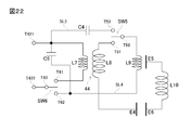
- a capacitor C5 is added between the conductive lines SL3 and SL4 as shown in FIG. 22, a capacitor C5 is provided instead of the capacitor C4 as shown in FIG. 23, and both the capacitors C4 and C5 are omitted. You may do it.
- the electrode E4 may be divided into partial electrodes E4_1 and E4_2.
- the power receiving device 50a corresponds only to the electric field coupling method
- the power receiving device 50b corresponds to only the magnetic field coupling method.
- the configurations of the power receiving devices 50a and 50b may be integrated to prepare a power receiving device corresponding to both the electric field coupling method and the magnetic field coupling method.
- the power transmission device 40 is configured as shown in FIG.
- the power transmission device 40 shown in FIG. 25 is the same as the power transmission device 40 shown in FIG. 18 except that switches SW7 and SW8 are added and the control circuit 46 controls the switches SW7 and SW8 in addition to the switches SW5 and SW6. Therefore, the redundant description regarding the same configuration is omitted as much as possible.
- the capacitor C4 forms an LC resonance circuit together with the wound body L9, and the resonance frequency of the LC resonance circuit is adjusted to be close to the frequency of the AC voltage generated by the inverter 42.
- the switch SW7 has a common terminal T70 and branch terminals T71 and T72.
- the common terminal T70 is connected to one output terminal T421 of the inverter 42
- the branch terminal T71 is connected to the branch terminal T52 of the switch SW5 via the capacitor C4
- the branch terminal T72 is connected to one end of the primary coil L7.
- the switch SW8 is provided between the branch terminal T51 of the switch SW5 and the branch terminal T62 of the switch SW6.
- common terminal T50 of switch SW5 is connected to branch terminal T51, and common terminal T60 of switch SW6 is connected to branch terminal T61.
- the common terminal T70 of the switch SW7 is connected to the branch terminal T72, and the switch SW8 is turned on.
- One end of the wound body L9 is connected to one end of the secondary coil L8 that forms the step-up transformer 44, and the other end of the wound body L9 is opened. Further, one end and the other end of the wound body L9 are short-circuited by the switch SW8. Further, one end and the other end of the primary coil L7 constituting the step-up transformer 44 are connected to one output end T421 and the other output end T422 of the inverter 42, respectively.
- the conductive line short-circuited by the switch SW8 is defined as “SL5”, the conductive line SL5 forms an electric field coupling electrode together with the wound body L9.
- the AC voltage output from one output terminal T421 and the other output terminal T422 of the inverter 42 is boosted by the step-up transformer 44 and then applied to the conductive line SL5, the wound body L9, and the electrode E4.
- the conductive line SL5 and the wound body L9 are electrically coupled to the electrode E5, and the electrode E4 is electrically coupled to the electrode E6.
- An AC voltage having the same frequency as the AC voltage applied to the conductive line SL5, the wound body L9 and the electrode E4 is excited on the electrodes E5 and E6.
- the excited AC voltage is stepped down by the step-down transformer 52 and then converted into a DC voltage by the rectifying and smoothing circuit 54.
- the charging circuit 56 charges the battery BT based on the DC voltage thus converted.
- common terminal T50 of switch SW5 is connected to branch terminal T52, and common terminal T60 of switch SW6 is connected to branch terminal T62.
- the common terminal T70 of the switch SW7 is connected to the branch terminal T71, and the switch SW8 is turned off. Therefore, one end of wound body L9 is connected to one output end T421 of inverter 42 via switch SW5, capacitor C4, and switch SW7.
- the other end of the wound body L9 is connected to the other output terminal T422 of the inverter via the switch SW6. At this time, the wound body L9 functions as an electromagnetic induction coil for magnetic field coupling.
- the alternating voltage output from one output end T421 and the other output end T422 of the inverter 42 is applied to one end and the other end of the wound body L9.
- the wound body L9 is magnetically coupled to the electromagnetic induction coil L12.
- an AC voltage having the same frequency as the AC voltage applied to the wound body L9 is excited in the electromagnetic induction coil L12.
- the rectifying and smoothing circuit 54 converts the excited AC voltage into a DC voltage
- the charging circuit 56 charges the battery BT based on the converted DC voltage.
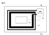
- the electrode E4 and the wound body L9 are provided in the power transmission device 40 in the manner shown in FIGS. 27 (A) and 27 (B).
- the power transmission device 40 has a rectangular parallelepiped housing THS, and the electrode E4 is formed in a rectangular plate shape.
- the electrode E4 is provided approximately at the center of the upper surface of the housing THS in such a posture that the orientation of the upper surface thereof matches the orientation of the upper surface of the housing THS.
- the wound body L9 is provided on the upper surface of the housing THS so that the winding axis is orthogonal to the upper surface of the housing THS and surrounds the electrode E4.
- the electrode E4 is provided with a space near the center of the opening of the wound body L9 as shown in FIGS. 27A and 27B, so that the eddy current caused by the proximity of the wound body on the power receiving device side can be reduced. Occurrence can be reduced.
- a ground electrode GND is provided on the lower surface of the housing THS.
- the ground electrode GND is also formed in a rectangular plate shape, and is provided at substantially the center of the lower surface of the housing THS so that the orientation of the lower surface coincides with the orientation of the lower surface of the housing THS.
- both the electrode E4 and the wound body L9 are covered with the ground electrode GND.
- the ground electrode GND having such a size also functions as a shield that suppresses radiation of an electric field or a magnetic field during power transmission to the power receiving device 50a or 50b.
- components or circuits other than the wound body L9 and the electrode E4 are housed in the power transmission module 48.
- the magnetic sheet can be attached to the surface of the ground electrode GND (winding body L9 side) so that it can be efficiently coupled to the winding body on the power receiving apparatus side.
- the power receiving device 50a adopting the electric field coupling method is configured as shown in FIG.
- the power receiving device 50a includes a rectangular parallelepiped housing RHS.
- the electrodes E5 and E6 are formed in a plate shape such that the contours forming the main surfaces are rectangular. However, regarding the size of the contour, the electrode E5 is much larger than the electrode E6.
- the electrode E5 has a rectangular hole penetrating from the upper surface toward the lower surface, and the size of the rectangle forming the hole is larger than the size of the main surface of the electrode E6.
- the electrodes E5 and E6 are provided at the center of the upper surface of the housing RHS so that the orientation of the upper surface of each of the electrodes E5 and E6 matches the orientation of the upper surface of the housing RHS.
- the electrode E6 is received in a hole provided in the electrode E5.
- power reception device 50 a is placed on power transmission device 40 with its upper surface facing the upper surface of power transmission device 40.
- the size of the main surface of the housing RHS that forms the power receiving device 50 a is about 2/3 of the size of the main surface of the housing THS that forms the power transmitting device 40.
- the size of the main surface of the electrode E6 provided in the power receiving device 50a is slightly larger than the size of the main surface of the electrode E4 provided in the power transmission device 40.
- the size of the electrode E5 provided in the power receiving device 50a is adjusted so that the electrode E5 partially overlaps the wound body L9 in a state where the electrode E4 is positioned so as to be covered by the electrode E6.
- the power receiving device 50b adopting the magnetic field coupling method is also configured as shown in FIG. According to FIG. 28 (B), the power receiving device 50b has a rectangular parallelepiped housing RHS.
- the wound body L12 is provided on the upper surface of the housing RHS so that its winding axis is orthogonal to the upper surface of the housing RHS.
- power reception device 50 b is placed on power transmission device 40 with the upper surface facing the upper surface of power transmission device 40.
- the size of the main surface of the housing RHS that forms the power receiving device 50 b is much smaller than the size of the main surface of the housing THS that forms the power transmitting device 40. Therefore, a plurality of power receiving devices 50b, 50b,... Can be placed inside the wound body L9 provided in the power transmitting device 40.
- the wound body L9 functions as one electrode for power transmission during power transmission according to the electric field coupling method, and also functions as an electromagnetic induction coil during power transmission according to the magnetic field coupling method.
- the electrode E4 functions as the other electrode for power transmission during power transmission according to the electric field coupling method.
- complication of a circuit structure can be suppressed by sharing the wound body L9 as a power transmission electrode and an electromagnetic induction coil.
- the conductive line SL5 also functions as one electrode for power transmission according to the electric field coupling method. Thereby, the power transmission performance is improved.
- the line width of the wound body L9 provided in the power transmission device 40 is uniform, but as shown in FIG. 31, the line width of the wound body L9 is partially increased. Also good.
- the coupling capacity with the power receiving device 50a is increased, high power transmission is possible, or power transmission efficiency is improved.
- a single electrode E4 is provided in the power transmission device 40.
- the electrode E4 may be divided into partial electrodes E4_1 and E4_2 as shown in FIG. 24 described above, and the partial electrodes E4_1 and E4_2 may be provided on the upper surface of the housing THS as shown in FIG.
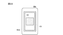
- the power receiving device 50a employing the electric field coupling method is configured as shown in FIG.
- the power receiving device 50a illustrated in FIG. 33 is substantially the same as the power receiving device 50a illustrated in FIG. 28A, except that the size thereof is approximately half the size of the power receiving device 50a illustrated in FIG. .
- power reception device 50a is placed on power transmission device 40 with the upper surface facing the upper surface of power transmission device 40.
- the size of the main surface of the housing RHS that forms the power receiving device 50 a is about 1/3 of the size of the main surface of the housing THS that forms the power transmitting device 40.
- the size of the main surface of the electrode E6 provided in the power receiving device 50a is slightly larger than the size of the main surface of the electrode E4_1 or E4_2 provided in the power transmission device 40.
- the size of the electrode E5 provided in the power receiving device 50a is adjusted so that the electrode E5 partially overlaps the wound body L9 in a state where the electrode E4_1 or E4_2 is positioned so as to be covered by the electrode E6.
- the electrodes E4_1 and E4_2 are always connected to the secondary coil L8 constituting the step-up transformer 44.
- the connection with the secondary coil L8 may be turned on / off depending on whether or not it is covered with the electrode E6 of the power receiving device 50a.
Landscapes
- Engineering & Computer Science (AREA)
- Computer Networks & Wireless Communication (AREA)
- Power Engineering (AREA)
- Charge And Discharge Circuits For Batteries Or The Like (AREA)
Abstract
受電装置20は、電界結合方式または磁界結合方式に対応する送電装置から伝送された電力を受電する。受電装置20において、巻回体L4および電極E3はいずれも導電性を有する。また、整流平滑回路24は、交流電圧が印加される一方入力端T241および他方入力端T242を有し、交流電圧を直流電圧に変換する。降圧トランス22は、電界結合時に巻回体L4の一方端および電極E3を一方入力端T241および他方入力端T242に電気的に接続する。また、導電線SL1およびSL2は、磁界結合時に巻回体L4の一方端および他方端を一方入力端T241および他方入力端T242に電気的に接続する。
Description
この発明は、受電装置、送電装置および電力伝送システムに関し、特に電界結合方式に対応する、受電装置、送電装置および電力伝送システムに関する。
電界結合方式で電力を伝送する装置の一例が特許文献1に開示されている。この装置は、互いに近距離に位置するエネルギー生成装置および消費装置で構成される。また、この装置は、非対称発振電気双極子間の相互作用の形でモデル化され、この双極子は、2つの電極間に置かれた高圧高周波発生器または高圧高周波電荷で構成される。これらの双極子は、互いに相互インフルエンスを及ぼす。電気エネルギーおよび/または情報は、ゆるやかに変化する可変状態であらゆる帯電導体の集合を取り囲むクーロン場を利用して遠隔搬送される。
また、磁界結合方式で電力伝送を行うシステムの一例が特許文献2に開示されている。このシステムは、送電部を有する親機と受電部を有する子機とによって形成される。送電部は電源の出力に基づく交番磁界を介して電力を送電し、受電部は外部から到来する交番磁界を電気量に変換して電力を受電する。
しかし、電界結合方式と磁界結合方式とでは全く異なる原理が採用されるため、1つの装置でいずれの方式にも対応しようとすると、回路構成の複雑化を引き起こすおそれがある。
それゆえに、この発明の主たる目的は、回路構成の複雑化を抑制しつつ磁界結合方式および電界結合方式の両方に対応できる、受電装置、送電装置および電力伝送システムを提供することである。
この発明に従う受電装置(20:実施例で相当する参照符号。以下同じ)は、電界結合方式および磁界結合方式の少なくとも一方を採用する送電装置(10a, 10b)から伝送された電力を受電する受電装置であって、導電性を有する巻回体(L4)、導電性を有する板状体(E3, E3_1, E3_2)、交流電圧が印加される一方入力端(T241, T301, T321)および他方入力端(T242, T302, T322)を有し、交流電圧を直流電圧に変換する変換手段(24, 30, 32)、電界結合時に巻回体の一方端および板状体を一方入力端および他方入力端に電気的に接続する第1接続手段(22)、および磁界結合時に巻回体の一方端および他方端を一方入力端および他方入力端に電気的に接続する第2接続手段(SL1, SL2)を備える。
好ましくは、第1接続手段は、巻回体の一方端および板状体とそれぞれ接続される一方端および他方端を有する一次コイル(L5)、および一方入力端および他方入力端とそれぞれ接続される一方端および他方端を有しかつ一次コイルとともに降圧トランス(22)を形成する二次コイル(L6)を含み、第2接続手段は、巻回体の一方端を一方入力端と接続する第1導電線(SL1)、および巻回体の他方端を他方入力端と接続する第2導電線(SL2)を含む。
或る局面では、第1導電線に設けられた第1コンデンサ(C1)がさらに備えられる。
他の局面では、第1導電線および第2導電線の間に設けられた第2コンデンサ(C2)がさらに備えられる。
その他の局面では、巻回体の一方端の接続先を一次コイルの一方端と第1導電線との間で切り換える第1切り換え手段(SW1)、および他方入力端の接続先を二次コイルの他方端と第2導電線との間で切り換える第2切り換え手段(SW2)がさらに備えられる。
さらにその他の局面では、変換手段は、電界結合方式に対応する第1電圧変換手段(32)、および磁界結合方式に対応する第2電圧変換手段(30)を含み、一方入力端は、第1電圧変換手段に割り当てられた第1の一方電圧入力端(T321)、および第2電圧変換手段に割り当てられた第2の一方電圧入力端(T301)を含み、他方入力端は、第1電圧変換手段に割り当てられた第1の他方電圧入力端(T322)、および第2電圧変換手段に割り当てられた第2の他方電圧入力端(T302)を含み、二次コイルの一方端および他方端は第1の一方電圧入力端および第1の他方電圧入力端にそれぞれ接続され、第1導電線および第2導電線は第2の一方電圧入力端および第2の他方電圧入力端にそれぞれ接続される。
さらに好ましくは、巻回体の一方端の接続先を一次コイルの一方端と第1導電線との間で切り換える第3切り換え手段(SW3)、および第2導電線を断続する第4切り換え手段(SW4)がさらに備えられる。
好ましくは、板状体は複数の部分板状体(E3_1, E3_2)を含む。
この発明に従う送電装置(40)は、電界結合方式および磁界結合方式の少なくとも一方を採用する受電装置(50a, 50b)に電力を伝送する送電装置であって、導電性を有する巻回体(L9)、導電性を有する板状体(E4, E4_1, E4_2)、交流電圧が印加される一方出力端(T421)および他方出力端(T422)を有し、直流電圧を交流電圧に変換する変換手段(42)、電界結合時に巻回体の一方端および板状体を一方出力端および他方出力端に電気的に接続する第1接続手段(44)、および磁界結合時に巻回体の一方端および他方端を一方出力端および他方出力端に電気的に接続する第2接続手段(SL3, SL4)を備える。
好ましくは、第1接続手段は、一方出力端および他方出力端とそれぞれ接続される一方端および他方端を有する一次コイル(L7)、および巻回体の一方端および板状体とそれぞれ接続される一方端および他方端を有しかつ一次コイルとともに昇圧トランス(44)を形成するする二次コイル(L8)を含み、第2接続手段は、巻回体の一方端を一方出力端と接続する第1導電線(SL3)、および巻回体の他方端を他方出力端と接続する第2導電線(SL4)を含む。
或る局面では、第1導電線に設けられた第1コンデンサ(C4)がさらに備えられる。
他の局面では、第1導電線および第2導電線の間に設けられた第2コンデンサ(C5)がさらに備えられる。
その他の局面では、巻回体の一方端の接続先を二次コイルの一方端と第1導電線との間で切り換える第1切り換え手段(SW5)、および他方出力端の接続先を一次コイルの他方端と第2導電線との間で切り換える第2切り換え手段(SW6)がさらに備えられる。
この発明に従う電力伝送システムは、電界結合方式および磁界結合方式の少なくとも一方を採用する送電装置(10a, 10b)、および送電装置から伝送された電力を受電する受電装置(20)を備える電力伝送システムであって、受電装置は、導電性を有する巻回体(L4)、導電性を有する板状体(E3, E3_1, E3_2)、交流電圧が印加される一方入力端(T241, T301, T321)および他方入力端(T242, T302, T322)を有し、交流電圧を直流電圧に変換する変換手段(24, 30, 32)、電界結合時に巻回体の一方端および板状体を一方入力端および他方入力端に電気的に接続する第1接続手段(22)、および磁界結合時に巻回体の一方端および他方端を一方入力端および他方入力端に電気的に接続する第2接続手段(SL1, SL2)を備える。
この発明に従う電力伝送システムは、電界結合方式および磁界結合方式の少なくとも一方を採用する受電装置(50a, 50b)、および受電装置に電力を伝送する送電装置(40)を備える電力伝送システムであって、送電装置は、導電性を有する巻回体(L9)、導電性を有する板状体(E4, E4_1, E4_2)、交流電圧が印加される一方出力端(T421)および他方出力端(T422)を有し、直流電圧を交流電圧に変換する変換手段(42)、電界結合時に巻回体の一方端および板状体を一方出力端および他方出力端に電気的に接続する第1接続手段(44)、および磁界結合時に巻回体の一方端および他方端を一方出力端および他方出力端に電気的に接続する第2接続手段(SL3, SL4)を備える。
この発明によれば、巻回体は、電界結合方式に従う受電時または送電時に受電用または送電用の一方電極として機能するとともに、磁界結合方式に従う受電時または送電時に電磁誘導コイルとして機能する。また、板状体は、電界結合方式に従う受電時または送電時に受電用または送電用の他方電極として機能する。このように、巻回体を受電用または送電用の電極および電磁誘導コイルとして共用することで、回路構成の複雑化を抑制することができる。
この発明の上述の目的,その他の目的,特徴および利点は、図面を参照して行う以下の実施例の詳細な説明から一層明らかとなろう。
この実施例の電力伝送システムは、図1(A)に示す送電装置10aまたは図1(B)に示す送電装置10bと、図2に示す受電装置20とによって形成される。図1(A)に示す送電装置10aは電界結合方式に対応し、図1(B)に示す送電装置10bは磁界結合方式に対応する。また、図2に示す受電装置20は、電界結合方式および磁界結合方式の両方に対応する。
図1(A)に示す送電装置10aにおいて、インバータ12は、直流電源Vccから出力された直流電圧を交流電圧に変換する。変換された交流電圧は、昇圧トランス14を形成する一次コイルL1に印加される。二次コイルL2は、一次コイルL1の巻数よりも大きい巻数を有し、一次コイルL1とともに昇圧トランス14を形成する。また、二次コイルL2の一方端および他方端はそれぞれ、電界結合用の電極E1およびE2と接続される。電極E1およびE2には、昇圧トランス14によって昇圧された交流電圧が印加される。
図1(B)に示す送電装置10bでも、直流電源Vccから出力された直流電圧はインバータ12によって交流電圧に変換される。ただし、変換された交流電圧は、磁界結合用の電磁誘導コイルL3に印加される。
図2を参照して、スイッチSW1は共通端子T10と分岐端子T11およびT12とを有し、スイッチSW2は共通端子T20と分岐端子T21およびT22とを有する。巻回体L4の一方端および他方端はそれぞれ、スイッチSW1の共通端子T10およびスイッチSW2の分岐端子T21と接続される。また、スイッチSW1の分岐端子T12および板状の電極E3はそれぞれ、二次コイルL6とともに降圧トランスL5を形成する一次コイルL5の一方端および他方端と接続される。なお、二次コイルL6は、一次コイルL5の巻数よりも小さい巻数を有する。
二次コイルL6の一方端は整流平滑回路24に設けられた一方入力端T241と接続され、二次コイルL6の他方端はスイッチSW2の分岐端子T22と接続される。スイッチSW2の共通端子T20は、整流平滑回路24に設けられた他方入力端T242と接続される。整流平滑回路24の一方入力端T241はまた、コンデンサC1を介してスイッチSW1の分岐端子T11と接続される。
なお、以下では、分岐端子T12と整流平滑回路24の一方入力端T241とを接続する導電線を特に“SL1”と定義し、巻回体L4の他方端とスイッチSW2の分岐端子T21とを接続する導電線を特に“SL2”と定義する。また、コンデンサC1は巻回体L4とともにLC共振回路をなし、このLC共振回路の共振周波数はインバータ12によって生成される交流電圧の周波数の近傍に調整される。
図3(A)を参照して、電界結合時、スイッチSW1の共通端子T10は分岐端子T11と接続され、スイッチSW2の共通端子T20は分岐端子T21と接続される。巻回体L4の一方端は降圧トランス22を形成する一次コイルL5の一方端と接続され、巻回体L4の他方端は開放される。また、降圧トランス22を構成する二次コイルL6の他方端は整流平滑回路24の他方入力端T242と接続される。このとき、巻回体L4は、電界結合用の電極として機能する。
受電装置20が送電装置10aに近づけられると、巻回体L4および電極E3が電極E1およびE2と電界結合される。この結果、電極E1およびE2に印加された交流電圧と同じ周波数を有する交流電圧が、巻回体L4および電極E3に励起される。励起された交流電圧は、降圧トランス22を介して整流平滑回路24の一方入力端T241および他方入力端T242に印加される。
図3(B)を参照して、磁界結合時、スイッチSW1の共通端子T10は分岐端子T12と接続され、スイッチSW2の共通端子T20は分岐端子T22と接続される。巻回体L4の一方端はスイッチSW1およびコンデンサC1を介して整流平滑回路24の一方入力端T241と接続され、巻回体L4の他方端はスイッチSW2を介して整流平滑回路24の他方入力端T242と接続される。このとき、巻回体L4は、磁界結合用の電磁誘導コイルとして機能する。
受電装置20が送電装置10bに近づけられると、巻回体L4が電磁誘導コイルL3と磁界結合される。この結果、電磁誘導コイルL3に印加された交流電圧と同じ周波数を有する交流電圧が、巻回体L4に励起される。励起された交流電圧は、整流平滑回路24の一方入力端T241および他方入力端T242に印加される。
整流平滑回路24は、こうして印加された交流電圧を整流平滑して直流電圧を生成し、生成された直流電圧を充電回路26に供給する。充電回路26は、供給された直流電圧に基づいてバッテリBTを充電する。
整流平滑回路24によって生成された直流電圧は、制御回路28にも与えられる。制御回路28は、与えられた直流電圧を参照してスイッチSW1およびSW2の設定を制御する。具体的には、制御回路28は、図4に示すフロー図に従う処理を実行する。
まずステップS1で、スイッチSW1の共通端子T10を分岐端子T11に接続し、かつスイッチSW2の共通端子T20を分岐端子T21に接続する。ステップS3では整流平滑回路24から与えられた直流電圧の電圧値を検出し、ステップS5では検出された電圧値が規定値以上であるか否かを判別する。
判別結果がNOであれば、ステップS7でスイッチSW1およびSW2の接続を変更する。スイッチSW1に設けられた共通端子T10の接続先は分岐端子T11およびT12の間で変更され、スイッチSW2に設けられた共通端子T20の接続先は分岐端子T21およびT22の間で変更される。変更が完了すると、ステップS3に戻る。
スイッチSW1の共通端子T10が分岐端子T11と接続され、かつスイッチSW2の共通端子T20が分岐端子T21と接続された状態で、ステップS5の判別結果がYESを示せば、電界結合方式に対応する送電装置10aが受電装置20に近づけられたとみなし、電界結合方式に従う受電を開始する。
これに対して、スイッチSW1の共通端子T10が分岐端子T12と接続され、かつスイッチSW2の共通端子T20が分岐端子T22と接続された状態で、ステップS5の判別結果がYESを示せば、磁界結合方式に対応する送電装置10bが受電装置20に近づけられたとみなし、磁界結合方式に従う受電を開始する。
ここで、ステップS5の規定値は、電界結合方式の場合と磁界結合方式の場合で、同じ値であってもよいし、異なる値であってもよい。
また、上記では、整流平滑後の電圧の値により、電界結合方式と磁界結合方式を切り替えているが、送電装置、受電装置にそれぞれ別途送信側通信回路と受信側通信回路を設けて無線通信を行うことにより、電磁結合方式と磁界結合方式を切り替えてもよい。
すなわち、例えば以下のように行う。
電界結合方式の送電装置の送信側通信回路は、受信側通信回路から電界ステータス信号を受信したときに受信側通信回路へ電界ステータス信号を送信し、電界結合ホールド信号を受信したときに送電を開始させる機能を持たせておく。磁界結合方式の送電装置の送信側通信回路は、受信側通信回路から磁界ステータス信号を受信したときに受信側通信回路へ磁界ステータス信号を送信し、磁界結合ホールド信号を受信したときに送電を開始させる機能を持たせておく。
受電装置の通信回路は、送電装置へ電界ステータス信号を送付し、送電装置から電界ステータス信号を受信したとき、電界結合方式に対応する送電装置10aが受電装置20に近づけられたとみなし、送電装置へ電界結合ホールド信号を送信し、電界結合方式に従う受電を開始する。また、受電装置の通信回路が送電装置へ電界ステータス信号を送付しタイムアウトになった場合には、磁界ステータス信号を送付し、送電装置から磁界ステータス信号を受信したときには、磁界結合方式に対応する送電装置10bが受電装置20に近づけられたとみなし、送電装置へ磁界結合ホールド信号を送信し、磁界結合方式に従う受電を開始する。なお、受信装置の通信回路が磁界ステータス信号を送付しタイムアウトになったときには、上記の電界ステータス信号を送付するところから繰り返す。
巻回体L4および電極E3は、図5(A)に示す態様で受電装置20に設けられる。図5(A)によれば、巻回体L4は円板状に形成され、電極E3は矩形の板状に形成される。また、受電装置20は、直方体状の筐体RHSを有する。巻回体L4は、巻回軸が筐体RHSの主面に直交する姿勢で、筐体RHSの主面の中央に設けられる。一方、電極E3は、その主面の向きが筐体RHSの主面の向きと一致する姿勢で、筐体RHSの主面の長さ方向一方端側の位置に設けられる。
以上の説明から分かるように、送電装置10aは電界結合方式に対応し、送電装置10bは磁界結合方式に対応する。受電装置20は、送電装置10aまたは10bから伝送された電力を受電する。受電装置20において、巻回体L4および電極E3はいずれも導電性を有する。また、整流平滑回路24は、交流電圧が印加される一方入力端T241および他方入力端T242を有し、交流電圧を直流電圧に変換する。降圧トランス22は、電界結合時に巻回体L4の一方端および電極E3を一方入力端T241および他方入力端T242に電気的に接続する。また、導電線SL1およびSL2は、磁界結合時に巻回体L4の一方端および他方端を一方入力端T241および他方入力端T242に電気的に接続する。
このように、巻回体L4は、電界結合方式に従う受電時に受電用の一方電極として機能するとともに、磁界結合方式に従う受電時に電磁誘導コイルとして機能する。また、電極E3は、電界結合方式に従う受電時に受電用の他方電極として機能する。このように、巻回体L4を受電電極および電磁誘導コイルとして共用することで、回路構成の複雑化を抑制することができる。
なお、巻回体L4および電極E3は、図5(B)~図5(F)に示す態様で受電装置20に設けるようにしてもよい。図5(B)によれば、巻回体L4が筐体RHSの主面の長さ方向一方端側の位置に設けられ、電極E3が筐体RHSの主面の中央に設けられる。図5(C)によれば、巻回体L4が筐体RHSの主面の長さ方向一方端側の位置に設けられ、主面の面積が拡大された電極E3が筐体RHSの主面の中央よりも長さ方向他方端側の位置に設けられる。図5(D)~図5(F)に示す態様は、巻回体L4の主面の形状が矩形をなす点を除き、図5(A)~図5(C)と同様である。
また、図2に示す受電装置20では、導電線SL1にコンデンサC1を設けるようにしている。しかし、図6に示すようにコンデンサC2を導電線SL1およびSL2の間に追加したり、図7に示すようにコンデンサC1の代わりにコンデンサC2を設けたり、さらにはコンデンサC1およびC2の両方を省くようにしてもよい。
さらに、図2に示す受電装置20では、単一の電極E3を設けるようにしている。しかし、図8に示すように電極E3を部分電極E3_1およびE3_2に分割し、部分電極E3_1およびE3_2を図9(A)または図9(B)に示す態様で筐体RHSの主面に設けるようにしてもよい。図9(A)および図9(B)によれば、部分電極E3_1は筐体RHSの長さ方向一方端側に設けられ、部分電極E3_2は筐体RHSの長さ方向他方端側に設けられる。なお、巻回体L4は、図9(A)および図9(B)のいずれにおいても、筐体RHSの主面の中央に設けられる。
図9の構成を用いることによって、送電装置がどちらの向きであっても配置させることができる(置きやすい向きに置くことができる)メリットがある。
また、図1(A)および図1(B)によれば、送電装置10aは電界結合方式にのみ対応し、送電装置10bは磁界結合方式にのみ対応する。しかし、送電装置10aおよび10bの構成を統合し、電界結合方式および磁界結合方式の両方に対応する送電装置を準備するようにしてもよい。
図10を参照して、他の実施例の受電装置10は、磁界結合方式および電界結合方式にそれぞれ対応する整流平滑回路30および32が図2に示す整流平滑回路24の代わりに設けられ、これに対応して一部の構成が修正された点を除き、図2に示す整流平滑回路24と同様である。したがって、同様の構成に関する重複した説明は極力省略する。
図10によれば、スイッチSW3は共通端子T40と分岐端子T41よびT42を有する。また、整流平滑回路30は一方入力端T301および他方入力端T302を有し、整流平滑回路32は一方入力端T321および他方入力端T322を有する。共通端子T40は巻回体L4の一方端と接続され、分岐端子T42はコンデンサC1を介して整流平滑回路30の一方入力端T301と接続され、分岐端子T41は降圧トランス22を形成する一次コイルL5の一方端と接続される。
整流平滑回路30の他方入力端T302は、スイッチSW4を介して巻回体L4の他方端と接続される。また、整流平滑回路32の一方入力端T321および他方入力端T322は、降圧トランス22を形成する二次コイルL6の一方端および他方端とそれぞれ接続される。
なお、この受電装置においても、分岐端子T42と整流平滑回路30の一方入力端T301とを接続する導電線を“SL1”と定義し、巻回体L4の他方端と整流平滑回路30の他方入力端T302とを接続する導電線を“SL2”と定義する。
整流平滑回路30および32はいずれも、図11に示すように構成される。なお、この構成は、図2に示す整流平滑回路24においても採用される。図11によれば、ダイオードD1のカソードがダイオードD2のカソードと接続され、ダイオードD3のアノードがダイオードD4のアノードと接続される。ダイオードD1のアノードはダイオードD3のカソードと接続され、ダイオードD2のアノードはダイオードD4のカソードと接続される。
一方入力端T301またはT321はダイオードD1のアノードと接続され、他方入力端T302またはT322はダイオードD2のアノードと接続される。コンデンサC3の一方端はダイオードD1のカソードと接続され、コンデンサC3の他方端はダイオードD3のアノードと接続される。コンデンサC3の一方端および他方端はそれぞれ、充電回路26の一方入力端および他方入力端と接続される。
したがって、一方入力端T301(T321)および他方入力端T302(T322)に印加された交流電圧は、ダイオードD1~D4によって全波整流され、整流された電圧がコンデンサC3によって平滑される。交流電圧はこうして直流電圧に変換され、変換された直流電圧は充電回路26に供給される。
図2のように整流平滑回路を共通化させることによって回路全体をシンプルにすることができるため、装置全体の小型化には最適である。しかし一方で、例えば磁界結合時は2次側コイルL6の一端は接続された状態になるため、場合によっては2次側コイルL6と主にスイッチSW2で発生する寄生容量によって不要共振を発生させる原因となる。その場合は図10のような回路構成を用いることが効果的である。
図12を参照して、電界結合時、スイッチSW3の共通端子T30は分岐端子T31と接続され、スイッチSW4はオフされる。巻回体L4の一方端は降圧トランス22を形成する一次コイルL5の一方端と接続され、巻回体L4の他方端は開放される。このとき、巻回体L4は、電界結合用の電極として機能する。
受電装置10が送電装置10aに近づけられると、巻回体L4および電極E3が電極E1およびE2と電界結合される。この結果、電極E1およびE2に印加された交流電圧と同じ周波数を有する交流電圧が、巻回体L4および電極E3に励起される。励起された交流電圧は、降圧トランス22を介して整流平滑回路32の一方入力端T321および他方入力端T322に印加される。
図13を参照して、磁界結合時、スイッチSW3の共通端子T30は分岐端子T32と接続され、スイッチSW4はオンされる。巻回体L4の一方端は、スイッチSW3およびコンデンサC1を介して整流平滑回路30の一方入力端T301と接続される。また、巻回体L4の他方端は、スイッチSW4を介して整流平滑回路30の他方入力端T302と接続される。このとき、巻回体L4は、磁界結合用の電磁誘導コイルとして機能する。
受電装置20が送電装置10bに近づけられると、巻回体L4が電磁誘導コイルL3と磁界結合される。この結果、電磁誘導コイルL3に印加された交流電圧と同じ周波数を有する交流電圧が、巻回体L4に励起される。励起された交流電圧は、整流平滑回路30の一方入力端T301および他方入力端T302に印加される。
図10に戻って、制御回路28は、整流平滑回路30または32から与えられた直流電圧を参照して、スイッチSW3およびSW4の設定を制御する。具体的には、制御回路28は、図14に示すフロー図に従う処理を実行する。
まずステップS11で、スイッチSW3の共通端子T30を分岐端子T31に接続し、かつスイッチSW4をオフする。ステップS13では、整流平滑回路30または32から与えられた直流電圧の電圧値を検出し、ステップS15では検出された電圧値が規定値以上であるか否かを判別する。
判別結果がNOであれば、ステップS17でスイッチSW3およびSW4の接続を変更する。スイッチSW3に設けられた共通端子T30の接続先は分岐端子T31およびT32の間で変更され、スイッチSW4はオフ状態およびオン状態の間で変更される。変更が完了すると、ステップS13に戻る。
スイッチSW3の共通端子T30が分岐端子T31と接続され、かつスイッチSW4がオフされている状態で、整流平滑回路32から出力された直流電圧が規定値以上となると、受電装置20が電界結合方式に対応する送電装置10aに近づけられたとみなし、電界結合方式に従う受電を開始する。
これに対して、スイッチSW3の共通端子T30が分岐端子T32と接続され、かつスイッチSW4がオンされている状態で、整流平滑回路30から出力された直流電圧が規定値以上となると、受電装置20が磁界結合方式に対応する送電装置10bに近づけられたとみなし、磁界結合方式に従う受電を開始する。
ここで、ステップS15の規定値は、電界結合方式の場合と磁界結合方式の場合で、同じ値であってもよいし、異なる値であってもよい。
また、上記では、整流平滑後の電圧の値により、電界結合方式と磁界結合方式を切り替えているが、送電装置、受電装置にそれぞれ別途送信側通信回路と受信側通信回路を設けて無線通信を行うことにより、電磁結合方式と磁界結合方式を切り替えてもよい。
この実施例においても、巻回体L4は、電界結合方式に従う受電時に受電用の一方電極として機能するとともに、磁界結合方式に従う受電時に電磁誘導コイルとして機能する。また、電極E3は、電界結合方式に従う受電時に受電用の他方電極として機能する。このように、巻回体L4を受電電極および電磁誘導コイルとして共用することで、回路構成の複雑化を抑制することができる。
なお、図10に示す受電装置20では、導電線SL1にコンデンサC1を設けるようにしている。しかし、図15に示すようにコンデンサC2を導電線SL1およびSL2の間に追加したり、図16に示すようにコンデンサC1の代わりにコンデンサC2を設けたり、さらにはコンデンサC1およびC2の両方を省くようにしてもよい。また、図10に示す受電装置20では、単一の電極E3を設けるようにしている。しかし、図17に示すように電極E3を部分電極E3_1およびE3_2に分割するようにしてもよい。
他の実施例の電力伝送システムは、図18に示す送電装置40と、図19(A)に示す受電装置50aまたは図19(B)に示す受電装置50bとによって形成される。図18に示す送電装置40は、電界結合方式および磁界結合方式の両方に対応する。これに対して、図19(A)に示す受電装置50aは電界結合方式にのみ対応し、図19(B)に示す受電装置50bは磁界結合方式にのみ対応する。
図18に示す送電装置40において、インバータ42は、一方出力端T421および他方出力端T422を有し、直流電源Vccから出力された直流電圧を交流電圧に変換する。また、スイッチSW5は共通端子T50と分岐端子T51およびT52とを有し、スイッチSW6は共通端子T60と分岐端子T61およびT62とを有する。
インバータ42の一方出力端T421は昇圧トランス44を構成する一次コイルL7の一方端と接続され、一次コイルL7の他方端はスイッチSW6の分岐端子T61と接続され、そしてスイッチSW6の共通端子T60はインバータ42の他方出力端T422と接続される。
インバータ42の一方出力端T421はまた、コンデンサC4を介してスイッチSW5の分岐端子T52と接続される。スイッチSW5の共通端子T50は巻回体L9の一方端と接続され、巻回体L9の他方端はスイッチSW6の分岐端子T62と接続される。また、スイッチSW5の分岐端子T51は昇圧トランス44を構成する二次コイルL8の一方端と接続され、二次コイルL8の他方端は板状の電極E4と接続される。ここで、二次コイルL8は、一次コイルL7の巻数よりも大きい巻数を有する。
なお、以下では、インバータ42の一方出力端T421とスイッチSW5の分岐端子T52とを接続する導電線を特に“SL3”と定義し、スイッチSW6の分岐端子T62と巻回体L9の他方端とを接続する導電線を特に“SL4”と定義する。また、コンデンサC4は巻回体L9とともにLC共振回路をなし、このLC共振回路の共振周波数はインバータ42によって生成される交流電圧の周波数の近傍に調整される。
図19(A)を参照して、受電回路50aは、電界結合用の電極E5およびE6を有する。電極E5およびE6はそれぞれ、降圧トランス52を構成する一次コイルL10の一方端および他方端と接続される。降圧トランス52を構成する二次コイルL11は一次コイルの巻数よりも小さい巻数を有し、二次コイルL11の一方端および他方端はそれぞれ整流平滑回路54の一方入力端および他方入力端と接続される。整流平滑回路54の後段にはバッテリBTを充電する充電回路56が設けられる。
図19(B)を参照して、受電回路50bは、磁界結合用の電磁誘導コイルL12を有する。電磁誘導コイルL12の一方端および他方端はそれぞれ、整流平滑回路54の一方入力端および他方入力端と接続される。整流平滑回路54の後段にもバッテリBTを充電する充電回路56が設けられる。
図20(A)を参照して、電界結合時、スイッチSW5の共通端子T50は分岐端子T51と接続され、スイッチSW6の共通端子T60は分岐端子T61と接続される。巻回体L9の一方端は昇圧トランス44を形成する二次コイルL8の一方端と接続され、巻回体L9の他方端は開放される。また、昇圧トランス44を構成する一次コイルL7の他方端はインバータ42の他方出力端T422と接続される。このとき、巻回体L9は、電界結合用の電極として機能する。
インバータ42の一方出力端T421および他方出力端T422から出力された交流電圧は、昇圧トランス44によって昇圧された後、巻回体L9および電極E4に印加される。受電装置50aが送電装置40に近づけられると、巻回体L9および電極E4が電極E5およびE6と電界結合される。電極E5およびE6には、巻回体L9および電極E4に印加された交流電圧と同じ周波数を有する交流電圧が励起される。励起された交流電圧は、降圧トランス52で降圧された後、整流平滑回路54によって直流電圧に変換される。充電回路56は、こうして変換された直流電圧に基づいてバッテリBTを充電する。
図20(B)を参照して、磁界結合時、スイッチSW5の共通端子T50は分岐端子T52と接続され、スイッチSW6の共通端子T60は分岐端子T62と接続される。巻回体L9の一方端は、スイッチSW5およびコンデンサC4を介してインバータ42の一方出力端T421と接続される。また、巻回体L9の他方端は、スイッチSW6を介してインバータの他方出力端T422と接続される。このとき、巻回体L9は、磁界結合用の電磁誘導コイルとして機能する。
インバータ42の一方出力端T421および他方出力端T422から出力された交流電圧は、巻回体L9の一方端および他方端に印加される。受電装置50bが送電装置40に近づけられると、巻回体L9が電磁誘導コイルL12と磁界結合される。この結果、巻回体L9に印加された交流電圧と同じ周波数を有する交流電圧が、電磁誘導コイルL12に励起される。整流平滑回路54は励起された交流電圧を直流電圧に変換し、充電回路56は変換された直流電圧に基づいてバッテリBTを充電する。
図18に戻って、制御回路46は、インバータ42の出力側のインピーダンスを参照してスイッチSW5およびSW6の設定を制御する。具体的には、制御回路46は図21に示すフロー図に従う処理を実行する。
まずステップS21で、スイッチSW5の共通端子T50を分岐端子T51に接続し、スイッチSW6の共通端子T60を分岐端子T61に接続する。ステップS23ではインバータ42の出力側のインピーダンスを測定し、ステップS25では測定されたインピーダンスが規定範囲内であるか否かを判別する。判別結果がNOであれば、送電装置40の近傍には受電装置50aおよび50bのいずれも存在しないとみなし、ステップS23に戻る。
これに対して、ステップS25の判別結果がYESであれば、受電装置50aおよび50bのいずれか一方が送電装置50の近傍に存在するとみなし、受電装置50aおよび50bのいずれが存在するかをステップS27およびS29で判別する。ステップS27およびS29のいずれにおいても、ステップS23で測定されたインピーダンスが参照される。
インピーダンスが電界結合方式に対応する値を示せば、送電装置50の近傍に存在するのは受電装置50aであるとみなし、ステップS27でYESと判別する。この結果、スイッチSW5の共通端子T50が分岐端子T51に接続され、スイッチSW6の共通端子T60が分岐端子T61に接続された状態で、送電が開始される。
インピーダンスが電界結合方式に対応する値および磁界結合方式に対応する値のいずれとも異なれば、ステップS29でNOと判別し、ステップS31でスイッチSW5およびSW6の接続を変更する。スイッチSW5に設けられた共通端子T50の接続先は分岐端子T51およびT52の間で変更され、スイッチSW6に設けられた共通端子T60の接続先は分岐端子T61およびT62の間で変更される。変更が完了すると、ステップS23に戻る。
ステップS23で測定されたインピーダンスが磁界結合方式に対応する値を示せば、送電装置50の近傍に存在するのは受電装置50bであるとみなし、ステップS25およびステップS29でYESと判別する。この結果、スイッチSW5の共通端子T50が分岐端子T52に接続され、スイッチSW6の共通端子T60が分岐端子T62に接続された状態で、送電が開始される。
ここで、ステップS25の規定範囲は、電界結合方式の場合と磁界結合方式の場合で、同じ範囲であってもよいし、異なる範囲であってもよい。
また、上記では、インピーダンスの値により、電界結合方式と磁界結合方式を切り替えているが、送電装置、受電装置にそれぞれ別途送信側通信回路と受信側通信回路を設けて無線通信を行うことにより、電磁結合方式と磁界結合方式を切り替えてもよい。
すなわち、例えば以下のように行う。
送電装置の送信側通信回路は、受信側通信回路から電界ステータス信号を受信したときに受信側通信回路へ電界ステータス信号を送信し、その後、電界結合ホールド信号を受信したときに電界結合方式で送電を開始させる機能を持たせておく。また、受信側通信回路からの電界ステータス信号の受信がタイムアウトになったときは、受信側通信回路から磁界ステータス信号を受信したときに受信側通信回路へ磁界ステータス信号を送信し、その後、磁界結合ホールド信号を受信したときに磁界結合方式で送電を開始させる機能を持たせておく。なお、受信側通信回路からの磁界ステータス信号の受信がタイムアウトになったときは、上記の受信側通信回路からの電界ステータス信号を受信するところから繰り返す。
電界結合方式の受電装置の通信回路は、送電装置へ電界ステータス信号を送付し、送電装置から電界ステータス信号を受信したときには、電界結合方式に対応する受電装置50aが送電装置40に近づけられたとみなし、送電装置へ電界結合ホールド信号を送信し、電界結合方式に従う受電を開始する。また、磁界結合方式の受電装置の通信回路は、磁界ステータス信号を送付し、送電装置から磁界ステータス信号を受信したときには、磁界結合方式に対応する受電装置50bが送電装置40に近づけられたとみなし、送電装置へ磁界結合ホールド信号を送信し、磁界結合方式に従う受電を開始する。
以上の説明から分かるように、送電装置40は、電界結合方式に対応する受電装置50aおよび磁界結合方式に対応する受電装置50bのいずれか一方に電力を送電する。送電装置40において、巻回体L9および電極E4はいずれも、導電性を有する。インバータ24は、直流電圧を交流電圧に変換し、変換された交流電圧を一方出力端T421および他方出力端T422から出力する。昇圧トランス44は、電界結合時に巻回体L9の一方端および電極E4を一方出力端T421および他方出力端T422に電気的に接続する。また、導電線SL3およびSL4は、磁界結合時に巻回体L9の一方端および他方端を一方出力端T421および他方出力端T422に電気的に接続する。
このように、巻回体L9は、電界結合方式に従う送電時に送電用の一方電極として機能するとともに、磁界結合方式に従う送電時に電磁誘導コイルとして機能する。また、電極E4は、電界結合方式に従う送電時に送電用の他方電極として機能する。このように、巻回体L9を送電電極および電磁誘導コイルとして共用することで、回路構成の複雑化を抑制することができる。
なお、図18に示す送電装置40では、導電線SL3にコンデンサC4を設けるようにしている。しかし、図22に示すようにコンデンサC5を導電線SL3およびSL4の間に追加したり、図23に示すようにコンデンサC4の代わりにコンデンサC5を設けたり、さらにはコンデンサC4およびC5の両方を省くようにしてもよい。
また、図18に示す送電装置40では、単一の電極E4を設けるようにしている。しかし、図24に示すように電極E4を部分電極E4_1およびE4_2に分割するようにしてもよい。さらに、図19(A)および図19(B)によれば、受電装置50aは電界結合方式にのみ対応し、受電装置50bは磁界結合方式にのみ対応する。しかし、受電装置50aおよび50bの構成を統合し、電界結合方式および磁界結合方式の両方に対応する受電装置を準備するようにしてもよい。
その他の実施例の電力伝送システムでは、送電装置40は図25に示すように構成される。ただし、図25に示す送電装置40は、スイッチSW7およびSW8が追加され、制御回路46がスイッチSW5およびSW6に加えてスイッチSW7およびSW8も制御する点を除き、図18に示す送電装置40と同様であるため、同様の構成に関する重複した説明は極力省略する。なお、この実施例においても、コンデンサC4は巻回体L9とともにLC共振回路をなし、このLC共振回路の共振周波数はインバータ42によって生成される交流電圧の周波数の近傍に調整される。
スイッチSW7は、共通端子T70と分岐端子T71およびT72とを有する。共通端子T70はインバータ42の一方出力端T421と接続され、分岐端子T71はコンデンサC4を介してスイッチSW5の分岐端子T52と接続され、そして分岐端子T72は一次コイルL7の一方端と接続される。また、スイッチSW8は、スイッチSW5の分岐端子T51とスイッチSW6の分岐端子T62との間に設けられる。
図26(A)を参照して、電界結合時、スイッチSW5の共通端子T50は分岐端子T51と接続され、スイッチSW6の共通端子T60は分岐端子T61と接続される。また、スイッチSW7の共通端子T70は分岐端子T72と接続され、スイッチSW8はオンされる。
巻回体L9の一方端は昇圧トランス44を形成する二次コイルL8の一方端と接続され、巻回体L9の他方端は開放される。また、巻回体L9の一方端および他方端は、スイッチSW8によって短絡される。さらに、昇圧トランス44を構成する一次コイルL7の一方端および他方端はそれぞれ、インバータ42の一方出力端T421および他方出力端T422と接続される。スイッチSW8によって短絡された導電線を“SL5”と定義すると、導電線SL5は、巻回体L9とともに電界結合用の電極をなす。
インバータ42の一方出力端T421および他方出力端T422から出力された交流電圧は、昇圧トランス44によって昇圧された後、導電線SL5,巻回体L9および電極E4に印加される。図19(A)に示す受電装置50aが送電装置40に近づけられると、導電線SL5および巻回体L9が電極E5と電界結合され、電極E4が電極E6と電界結合される。電極E5およびE6には、導電線SL5,巻回体L9および電極E4に印加された交流電圧と同じ周波数を有する交流電圧が励起される。励起された交流電圧は、降圧トランス52で降圧された後、整流平滑回路54によって直流電圧に変換される。充電回路56は、こうして変換された直流電圧に基づいてバッテリBTを充電する。
図26(B)を参照して、磁界結合時、スイッチSW5の共通端子T50は分岐端子T52と接続され、スイッチSW6の共通端子T60は分岐端子T62と接続される。また、スイッチSW7の共通端子T70は分岐端子T71と接続され、スイッチSW8はオフされる。したがって、巻回体L9の一方端は、スイッチSW5,コンデンサC4およびスイッチSW7を介してインバータ42の一方出力端T421と接続される。また、巻回体L9の他方端は、スイッチSW6を介してインバータの他方出力端T422と接続される。このとき、巻回体L9は、磁界結合用の電磁誘導コイルとして機能する。
インバータ42の一方出力端T421および他方出力端T422から出力された交流電圧は、巻回体L9の一方端および他方端に印加される。図19(B)に示す受電装置50bが送電装置40に近づけられると、巻回体L9が電磁誘導コイルL12と磁界結合される。この結果、巻回体L9に印加された交流電圧と同じ周波数を有する交流電圧が、電磁誘導コイルL12に励起される。整流平滑回路54は励起された交流電圧を直流電圧に変換し、充電回路56は変換された直流電圧に基づいてバッテリBTを充電する。
電極E4および巻回体L9は、図27(A)および図27(B)に示す態様で送電装置40に設けられる。送電装置40は直方体状の筐体THSを有し、電極E4は矩形の板状に形成される。電極E4は、その上面の向きが筐体THSの上面の向きと一致する姿勢で、筐体THSの上面のほぼ中央に設けられる。巻回体L9は、巻回軸が筐体THSの上面に直交しかつ電極E4を囲むように、筐体THSの上面に設けられる。
なお、電極E4は図27(A)および図27(B)のように巻回体L9の開口部中央付近に間隔をもって設けることによって、受電装置側の巻回体が近接することによる渦電流の発生を軽減させることができる。
筐体THSの下面には、グランド電極GNDが設けられる。グランド電極GNDも矩形の板状に形成され、その下面の向きが筐体THSの下面の向きと一致する姿勢で、筐体THSの下面のほぼ中央に設けられる。筐体THSを下方から眺めると、電極E4および巻回体L9はいずれもグランド電極GNDによって覆われる。このようなサイズを有するグランド電極GNDは、受電装置50aまたは50bへの電力伝送時に電界または磁界の放射を抑制するシールドとしても機能する。なお、巻回体L9および電極E4以外の部品ないし回路は、送電モジュール48に収められる。
なお、図示はしないが、グランド電極GNDの表面(巻回体L9側)に磁性体シートを貼り付けておくことによって、受電装置側の巻回体と効率良く結合させることができる。
この実施例では、電界結合方式を採用する受電装置50aは図28(A)に示すように構成される。図28(A)によれば、受電装置50aは、直方体状の筐体RHSを有する。電極E5およびE6は、各々の主面をなす輪郭が矩形をなすように、板状に形成される。ただし、輪郭のサイズについては、電極E5が電極E6よりも格段に大きい。また、電極E5はその上面から下面に向かって貫通する矩形の孔を有し、孔をなす矩形のサイズは電極E6の主面のサイズよりも大きい。さらに、電極E5およびE6は、各々の上面の向きが筐体RHSの上面の向きと一致する姿勢で、筐体RHSの上面中央に設けられる。電極E6は、電極E5に設けられた孔に収められる。
図29を参照して、受電装置50aは、その上面が送電装置40の上面と対向する姿勢で送電装置40に載置される。図29から分かるように、受電装置50aをなす筐体RHSの主面のサイズは、送電装置40をなす筐体THSの主面のサイズの約2/3である。また、受電装置50aに設けられた電極E6の主面のサイズは、送電装置40に設けられた電極E4の主面のサイズよりも僅かに大きい。さらに、受電装置50aに設けられた電極E5のサイズは、電極E4が電極E6によって覆われるように位置決めされた状態において電極E5が巻回体L9と部分的に重なるように調整される。
この実施例ではまた、磁界結合方式を採用する受電装置50bは図28(B)に示すように構成される。図28(B)によれば、受電装置50bは、直方体状の筐体RHSを有する。巻回体L12は、その巻回軸が筐体RHSの上面と直交する姿勢で筐体RHSの上面に設けられる。
図30を参照して、受電装置50bは、その上面が送電装置40の上面と対向する姿勢で送電装置40に載置される。図30から分かるように、受電装置50bをなす筐体RHSの主面のサイズは、送電装置40をなす筐体THSの主面のサイズよりも格段に小さい。したがって、送電装置40に設けられた巻回体L9の内側には、複数の受電装置50b,50b,…を載置することができる。
この実施例においても、巻回体L9は、電界結合方式に従う送電時に送電用の一方電極として機能するとともに、磁界結合方式に従う送電時に電磁誘導コイルとして機能する。また、電極E4は、電界結合方式に従う送電時に送電用の他方電極として機能する。このように、巻回体L9を送電電極および電磁誘導コイルとして共用することで、回路構成の複雑化を抑制することができる。この実施例ではまた、導電線SL5が、電界結合方式に従う送電用の一方電極として機能する。これによって、電力伝送性能が向上する。
なお、この実施例では、送電装置40に設けられた巻回体L9の線幅は一律とされるが、図31に示すように巻回体L9の線幅を部分的に太くするようにしてもよい。これによって、巻回体L9を電界結合方式に従う送電用の一方電極として機能させるときに、受電装置50aとの結合容量が増大し、大電力の伝送が可能となり、或いは電力伝送効率が向上する。
また、この実施例では、単一の電極E4を送電装置40に設けるようにしている。しかし、電極E4を上述した図24のように部分電極E4_1およびE4_2に分割し、部分電極E4_1およびE4_2を図32に示すように筐体THSの上面に設けるようにしてもよい。この場合、電界結合方式を採用する受電装置50aは、図33に示すように構成される。なお、図33に示す受電装置50aは、そのサイズが図28(A)に示す受電装置50aのサイズの約半分である点を除き、図28(A)に示す受電装置50aとほぼ同じである。
図34を参照して、受電装置50aは、その上面が送電装置40の上面と対向する姿勢で送電装置40に載置される。図34から分かるように、受電装置50aをなす筐体RHSの主面のサイズは、送電装置40をなす筐体THSの主面のサイズの約1/3である。また、受電装置50aに設けられた電極E6の主面のサイズは、送電装置40に設けられた電極E4_1またはE4_2の主面のサイズよりも僅かに大きい。さらに、受電装置50aに設けられた電極E5のサイズは、電極E4_1またはE4_2が電極E6によって覆われるように位置決めされた状態において電極E5が巻回体L9と部分的に重なるように調整される。
なお、図24によれば、電極E4_1およびE4_2は昇圧トランス44を構成する二次コイルL8と常に接続される。しかし、受電装置50aの電極E6によって覆われたか否かによって二次コイルL8との接続をオン/オフするようにしてもよい。
10,40 …送電装置
20,50 …受電装置
12,42 …インバータ
22 …降圧トランス
24,30,32,54 …整流平滑回路
28,46 …制御回路
20,50 …受電装置
12,42 …インバータ
22 …降圧トランス
24,30,32,54 …整流平滑回路
28,46 …制御回路
Claims (15)
- 電界結合方式および磁界結合方式の少なくとも一方を採用する送電装置から伝送された電力を受電する受電装置であって、
導電性を有する巻回体、
導電性を有する板状体、
交流電圧が印加される一方入力端および他方入力端を有し、前記交流電圧を直流電圧に変換する変換手段、
電界結合時に前記巻回体の一方端および前記板状体を前記一方入力端および前記他方入力端に電気的に接続する第1接続手段、および
磁界結合時に前記巻回体の一方端および他方端を前記一方入力端および前記他方入力端に電気的に接続する第2接続手段を備える、受電装置。 - 前記第1接続手段は、前記巻回体の一方端および前記板状体とそれぞれ接続される一方端および他方端を有する一次コイル、および前記一方入力端および前記他方入力端とそれぞれ接続される一方端および他方端を有しかつ前記一次コイルとともに降圧トランスを形成する二次コイルを含み、
第2接続手段は、前記巻回体の一方端を前記一方入力端と接続する第1導電線、および前記巻回体の他方端を前記他方入力端と接続する第2導電線を含む、請求項1記載の受電装置。 - 前記第1導電線に設けられた第1コンデンサをさらに備える、請求項2記載の受電装置。
- 前記第1導電線および前記第2導電線の間に設けられた第2コンデンサをさらに備える、請求項2または3記載の受電装置。
- 前記巻回体の一方端の接続先を前記一次コイルの一方端と前記第1導電線との間で切り換える第1切り換え手段、および
前記他方入力端の接続先を前記二次コイルの他方端と前記第2導電線との間で切り換える第2切り換え手段をさらに備える、請求項2ないし4のいずれかに記載の受電装置。 - 前記変換手段は、前記電界結合方式に対応する第1電圧変換手段、および前記磁界結合方式に対応する第2電圧変換手段を含み、
前記一方入力端は、前記第1電圧変換手段に割り当てられた第1の一方電圧入力端、および前記第2電圧変換手段に割り当てられた第2の一方電圧入力端を含み、
前記他方入力端は、前記第1電圧変換手段に割り当てられた第1の他方電圧入力端、および前記第2電圧変換手段に割り当てられた第2の他方電圧入力端を含み、
前記二次コイルの一方端および他方端は前記第1の一方電圧入力端および前記第1の他方電圧入力端にそれぞれ接続され、
前記第1導電線および前記第2導電線は前記第2の一方電圧入力端および前記第2の他方電圧入力端にそれぞれ接続される、請求項2ないし4のいずれかに記載の受電装置。 - 前記巻回体の一方端の接続先を前記一次コイルの一方端と前記第1導電線との間で切り換える第3切り換え手段、および
前記第2導電線を断続する第4切り換え手段をさらに備える、請求項6記載の受電装置。 - 前記板状体は複数の部分板状体を含む、請求項1ないし7のいずれかに記載の受電装置。
- 電界結合方式および磁界結合方式の少なくとも一方を採用する受電装置に電力を伝送する送電装置であって、
導電性を有する巻回体、
導電性を有する板状体、
交流電圧が印加される一方出力端および他方出力端を有し、直流電圧を前記交流電圧に変換する変換手段、
電界結合時に前記巻回体の一方端および前記板状体を前記一方出力端および前記他方出力端に電気的に接続する第1接続手段、および
磁界結合時に前記巻回体の一方端および他方端を前記一方出力端および前記他方出力端に電気的に接続する第2接続手段を備える、送電装置。 - 前記第1接続手段は、前記一方出力端および前記他方出力端とそれぞれ接続される一方端および他方端を有する一次コイル、および前記巻回体の一方端および前記板状体とそれぞれ接続される一方端および他方端を有しかつ前記一次コイルとともに昇圧トランスを形成するする二次コイルを含み、
第2接続手段は、前記巻回体の一方端を前記一方出力端と接続する第1導電線、および前記巻回体の他方端を前記他方出力端と接続する第2導電線を含む、請求項9記載の送電装置。 - 前記第1導電線に設けられた第1コンデンサをさらに備える、請求項10記載の送電装置。
- 前記第1導電線および前記第2導電線の間に設けられた第2コンデンサをさらに備える、請求項10または11記載の送電装置。
- 前記巻回体の一方端の接続先を前記二次コイルの一方端と前記第1導電線との間で切り換える第1切り換え手段、および
前記他方出力端の接続先を前記一次コイルの他方端と前記第2導電線との間で切り換える第2切り換え手段をさらに備える、請求項9ないし12のいずれかに記載の送電装置。 - 電界結合方式および磁界結合方式の少なくとも一方を採用する送電装置、および前記送電装置から伝送された電力を受電する受電装置を備える電力伝送システムであって、
前記受電装置は、
導電性を有する巻回体、
導電性を有する板状体、
交流電圧が印加される一方入力端および他方入力端を有し、前記交流電圧を直流電圧に変換する変換手段、
電界結合時に前記巻回体の一方端および前記板状体を前記一方入力端および前記他方入力端に電気的に接続する第1接続手段、および
磁界結合時に前記巻回体の一方端および他方端を前記一方入力端および前記他方入力端に電気的に接続する第2接続手段を備える、電力伝送システム。 - 電界結合方式および磁界結合方式の少なくとも一方を採用する受電装置、および前記受電装置に電力を伝送する送電装置を備える電力伝送システムであって、
前記送電装置は、
導電性を有する巻回体、
導電性を有する板状体、
交流電圧が印加される一方出力端および他方出力端を有し、直流電圧を前記交流電圧に変換する変換手段、
電界結合時に前記巻回体の一方端および前記板状体を前記一方出力端および前記他方出力端に電気的に接続する第1接続手段、および
磁界結合時に前記巻回体の一方端および他方端を前記一方出力端および前記他方出力端に電気的に接続する第2接続手段を備える、電力伝送システム。
Priority Applications (1)
| Application Number | Priority Date | Filing Date | Title |
|---|---|---|---|
| JP2014557648A JP5737546B2 (ja) | 2013-02-05 | 2013-12-12 | 受電装置、送電装置および電力伝送システム |
Applications Claiming Priority (4)
| Application Number | Priority Date | Filing Date | Title |
|---|---|---|---|
| JP2013020740 | 2013-02-05 | ||
| JP2013-020740 | 2013-02-05 | ||
| JP2013142927 | 2013-07-08 | ||
| JP2013-142927 | 2013-07-08 |
Publications (1)
| Publication Number | Publication Date |
|---|---|
| WO2014122853A1 true WO2014122853A1 (ja) | 2014-08-14 |
Family
ID=51299457
Family Applications (1)
| Application Number | Title | Priority Date | Filing Date |
|---|---|---|---|
| PCT/JP2013/083286 Ceased WO2014122853A1 (ja) | 2013-02-05 | 2013-12-12 | 受電装置、送電装置および電力伝送システム |
Country Status (2)
| Country | Link |
|---|---|
| JP (1) | JP5737546B2 (ja) |
| WO (1) | WO2014122853A1 (ja) |
Cited By (2)
| Publication number | Priority date | Publication date | Assignee | Title |
|---|---|---|---|---|
| CN109941128A (zh) * | 2019-04-25 | 2019-06-28 | 西南交通大学 | 一种电场耦合式的电动汽车无线充电技术电压优化方法 |
| JP2023041491A (ja) * | 2021-09-13 | 2023-03-24 | 株式会社東芝 | 電子回路及び方法 |
Citations (3)
| Publication number | Priority date | Publication date | Assignee | Title |
|---|---|---|---|---|
| WO2012101907A1 (ja) * | 2011-01-26 | 2012-08-02 | 株式会社村田製作所 | 電力伝送システム |
| JP2012196126A (ja) * | 2011-03-03 | 2012-10-11 | Semiconductor Energy Lab Co Ltd | 受電装置、無線給電システム |
| JP2012253398A (ja) * | 2009-09-29 | 2012-12-20 | Univ Of Electro-Communications | 電力及び情報の伝送装置、システム、及び方法 |
Family Cites Families (1)
| Publication number | Priority date | Publication date | Assignee | Title |
|---|---|---|---|---|
| JP5096184B2 (ja) * | 2008-02-06 | 2012-12-12 | 株式会社ジャパンディスプレイイースト | 静電・誘導通信システム |
-
2013
- 2013-12-12 JP JP2014557648A patent/JP5737546B2/ja not_active Expired - Fee Related
- 2013-12-12 WO PCT/JP2013/083286 patent/WO2014122853A1/ja not_active Ceased
Patent Citations (3)
| Publication number | Priority date | Publication date | Assignee | Title |
|---|---|---|---|---|
| JP2012253398A (ja) * | 2009-09-29 | 2012-12-20 | Univ Of Electro-Communications | 電力及び情報の伝送装置、システム、及び方法 |
| WO2012101907A1 (ja) * | 2011-01-26 | 2012-08-02 | 株式会社村田製作所 | 電力伝送システム |
| JP2012196126A (ja) * | 2011-03-03 | 2012-10-11 | Semiconductor Energy Lab Co Ltd | 受電装置、無線給電システム |
Cited By (3)
| Publication number | Priority date | Publication date | Assignee | Title |
|---|---|---|---|---|
| CN109941128A (zh) * | 2019-04-25 | 2019-06-28 | 西南交通大学 | 一种电场耦合式的电动汽车无线充电技术电压优化方法 |
| JP2023041491A (ja) * | 2021-09-13 | 2023-03-24 | 株式会社東芝 | 電子回路及び方法 |
| JP7391920B2 (ja) | 2021-09-13 | 2023-12-05 | 株式会社東芝 | 電子回路及び方法 |
Also Published As
| Publication number | Publication date |
|---|---|
| JP5737546B2 (ja) | 2015-06-17 |
| JPWO2014122853A1 (ja) | 2017-01-26 |
Similar Documents
| Publication | Publication Date | Title |
|---|---|---|
| CN102870315B (zh) | 电力接收装置以及电力接收方法 | |
| JP5737545B2 (ja) | 受電装置、送電装置および電力伝送システム | |
| JP5908474B2 (ja) | 共振電力伝送装置及びその電力変換制御方法 | |
| JP4258505B2 (ja) | 給電システム | |
| JP6001355B2 (ja) | 非接触給電装置 | |
| JP6618006B2 (ja) | 無線電力伝送システムおよび送電装置 | |
| JP2015008625A5 (ja) | ||
| JP2013545430A (ja) | 電子機器の電力供給方法と、これを用いるソース電子機器及びターゲット電子機器 | |
| CN104104155A (zh) | 馈电单元和馈电系统 | |
| JPWO2014068989A1 (ja) | 無線電力伝送システム | |
| KR20120116802A (ko) | 중계기를 이용한 무선 전력 전송 시스템 및 무선 전력 수신기 | |
| JP6252051B2 (ja) | 電力変換器 | |
| JP2018207670A (ja) | ワイヤレス電力伝送システムの送電装置および前記ワイヤレス電力伝送システム | |
| JP5737546B2 (ja) | 受電装置、送電装置および電力伝送システム | |
| KR101670128B1 (ko) | 무선 전력 수신 장치 및 이를 구비하는 전자기기 | |
| JPWO2020066081A1 (ja) | ワイヤレス給電システム | |
| CN111279579A (zh) | 用于传输电能的谐振振荡回路 | |
| JP6652841B2 (ja) | 非接触受電装置 | |
| CN104218652B (zh) | Oled柔屏网络电子设备的无线充供电系统 | |
| JP2012034524A (ja) | 無線電力伝送装置 | |
| US20170149292A1 (en) | Resonant coil, wireless power transmitter using the same, wireless power receiver using the same | |
| JP6040510B2 (ja) | 電力伝送システム | |
| US9991749B2 (en) | Coil unit, wireless power feeding device, wireless power receiving device, and wireless power transmission device | |
| KR101946848B1 (ko) | 무선 전력 수신기 | |
| JP6112222B2 (ja) | 周波数特性測定方法 |
Legal Events
| Date | Code | Title | Description |
|---|---|---|---|
| 121 | Ep: the epo has been informed by wipo that ep was designated in this application |
Ref document number: 13874457 Country of ref document: EP Kind code of ref document: A1 |
|
| ENP | Entry into the national phase |
Ref document number: 2014557648 Country of ref document: JP Kind code of ref document: A |
|
| NENP | Non-entry into the national phase |
Ref country code: DE |
|
| 122 | Ep: pct application non-entry in european phase |
Ref document number: 13874457 Country of ref document: EP Kind code of ref document: A1 |