WO2014119463A1 - 導電性ペースト、導電性パターンの形成方法及び導電性パターン印刷物 - Google Patents
導電性ペースト、導電性パターンの形成方法及び導電性パターン印刷物 Download PDFInfo
- Publication number
- WO2014119463A1 WO2014119463A1 PCT/JP2014/051367 JP2014051367W WO2014119463A1 WO 2014119463 A1 WO2014119463 A1 WO 2014119463A1 JP 2014051367 W JP2014051367 W JP 2014051367W WO 2014119463 A1 WO2014119463 A1 WO 2014119463A1
- Authority
- WO
- WIPO (PCT)
- Prior art keywords
- conductive
- organic compound
- pattern
- conductive paste
- paste
- Prior art date
- Legal status (The legal status is an assumption and is not a legal conclusion. Google has not performed a legal analysis and makes no representation as to the accuracy of the status listed.)
- Ceased
Links
Images
Classifications
-
- C—CHEMISTRY; METALLURGY
- C09—DYES; PAINTS; POLISHES; NATURAL RESINS; ADHESIVES; COMPOSITIONS NOT OTHERWISE PROVIDED FOR; APPLICATIONS OF MATERIALS NOT OTHERWISE PROVIDED FOR
- C09D—COATING COMPOSITIONS, e.g. PAINTS, VARNISHES OR LACQUERS; FILLING PASTES; CHEMICAL PAINT OR INK REMOVERS; INKS; CORRECTING FLUIDS; WOODSTAINS; PASTES OR SOLIDS FOR COLOURING OR PRINTING; USE OF MATERIALS THEREFOR
- C09D5/00—Coating compositions, e.g. paints, varnishes or lacquers, characterised by their physical nature or the effects produced; Filling pastes
- C09D5/24—Electrically-conducting paints
-
- C—CHEMISTRY; METALLURGY
- C09—DYES; PAINTS; POLISHES; NATURAL RESINS; ADHESIVES; COMPOSITIONS NOT OTHERWISE PROVIDED FOR; APPLICATIONS OF MATERIALS NOT OTHERWISE PROVIDED FOR
- C09D—COATING COMPOSITIONS, e.g. PAINTS, VARNISHES OR LACQUERS; FILLING PASTES; CHEMICAL PAINT OR INK REMOVERS; INKS; CORRECTING FLUIDS; WOODSTAINS; PASTES OR SOLIDS FOR COLOURING OR PRINTING; USE OF MATERIALS THEREFOR
- C09D11/00—Inks
- C09D11/02—Printing inks
- C09D11/03—Printing inks characterised by features other than the chemical nature of the binder
- C09D11/037—Printing inks characterised by features other than the chemical nature of the binder characterised by the pigment
-
- C—CHEMISTRY; METALLURGY
- C09—DYES; PAINTS; POLISHES; NATURAL RESINS; ADHESIVES; COMPOSITIONS NOT OTHERWISE PROVIDED FOR; APPLICATIONS OF MATERIALS NOT OTHERWISE PROVIDED FOR
- C09D—COATING COMPOSITIONS, e.g. PAINTS, VARNISHES OR LACQUERS; FILLING PASTES; CHEMICAL PAINT OR INK REMOVERS; INKS; CORRECTING FLUIDS; WOODSTAINS; PASTES OR SOLIDS FOR COLOURING OR PRINTING; USE OF MATERIALS THEREFOR
- C09D11/00—Inks
- C09D11/02—Printing inks
- C09D11/10—Printing inks based on artificial resins
-
- C—CHEMISTRY; METALLURGY
- C09—DYES; PAINTS; POLISHES; NATURAL RESINS; ADHESIVES; COMPOSITIONS NOT OTHERWISE PROVIDED FOR; APPLICATIONS OF MATERIALS NOT OTHERWISE PROVIDED FOR
- C09D—COATING COMPOSITIONS, e.g. PAINTS, VARNISHES OR LACQUERS; FILLING PASTES; CHEMICAL PAINT OR INK REMOVERS; INKS; CORRECTING FLUIDS; WOODSTAINS; PASTES OR SOLIDS FOR COLOURING OR PRINTING; USE OF MATERIALS THEREFOR
- C09D11/00—Inks
- C09D11/52—Electrically conductive inks
-
- C—CHEMISTRY; METALLURGY
- C09—DYES; PAINTS; POLISHES; NATURAL RESINS; ADHESIVES; COMPOSITIONS NOT OTHERWISE PROVIDED FOR; APPLICATIONS OF MATERIALS NOT OTHERWISE PROVIDED FOR
- C09D—COATING COMPOSITIONS, e.g. PAINTS, VARNISHES OR LACQUERS; FILLING PASTES; CHEMICAL PAINT OR INK REMOVERS; INKS; CORRECTING FLUIDS; WOODSTAINS; PASTES OR SOLIDS FOR COLOURING OR PRINTING; USE OF MATERIALS THEREFOR
- C09D17/00—Pigment pastes, e.g. for mixing in paints
-
- H—ELECTRICITY
- H05—ELECTRIC TECHNIQUES NOT OTHERWISE PROVIDED FOR
- H05K—PRINTED CIRCUITS; CASINGS OR CONSTRUCTIONAL DETAILS OF ELECTRIC APPARATUS; MANUFACTURE OF ASSEMBLAGES OF ELECTRICAL COMPONENTS
- H05K1/00—Printed circuits
- H05K1/02—Details
- H05K1/09—Use of materials for the conductive, e.g. metallic pattern
- H05K1/092—Dispersed materials, e.g. conductive pastes or inks
-
- H—ELECTRICITY
- H05—ELECTRIC TECHNIQUES NOT OTHERWISE PROVIDED FOR
- H05K—PRINTED CIRCUITS; CASINGS OR CONSTRUCTIONAL DETAILS OF ELECTRIC APPARATUS; MANUFACTURE OF ASSEMBLAGES OF ELECTRICAL COMPONENTS
- H05K1/00—Printed circuits
- H05K1/02—Details
- H05K1/09—Use of materials for the conductive, e.g. metallic pattern
- H05K1/092—Dispersed materials, e.g. conductive pastes or inks
- H05K1/095—Dispersed materials, e.g. conductive pastes or inks for polymer thick films, i.e. having a permanent organic polymeric binder
-
- H—ELECTRICITY
- H05—ELECTRIC TECHNIQUES NOT OTHERWISE PROVIDED FOR
- H05K—PRINTED CIRCUITS; CASINGS OR CONSTRUCTIONAL DETAILS OF ELECTRIC APPARATUS; MANUFACTURE OF ASSEMBLAGES OF ELECTRICAL COMPONENTS
- H05K3/00—Apparatus or processes for manufacturing printed circuits
- H05K3/10—Apparatus or processes for manufacturing printed circuits in which conductive material is applied to the insulating support in such a manner as to form the desired conductive pattern
- H05K3/107—Apparatus or processes for manufacturing printed circuits in which conductive material is applied to the insulating support in such a manner as to form the desired conductive pattern by filling grooves in the support with conductive material
-
- H—ELECTRICITY
- H05—ELECTRIC TECHNIQUES NOT OTHERWISE PROVIDED FOR
- H05K—PRINTED CIRCUITS; CASINGS OR CONSTRUCTIONAL DETAILS OF ELECTRIC APPARATUS; MANUFACTURE OF ASSEMBLAGES OF ELECTRICAL COMPONENTS
- H05K3/00—Apparatus or processes for manufacturing printed circuits
- H05K3/10—Apparatus or processes for manufacturing printed circuits in which conductive material is applied to the insulating support in such a manner as to form the desired conductive pattern
- H05K3/12—Apparatus or processes for manufacturing printed circuits in which conductive material is applied to the insulating support in such a manner as to form the desired conductive pattern using thick film techniques, e.g. printing techniques to apply the conductive material or similar techniques for applying conductive paste or ink patterns
- H05K3/1275—Apparatus or processes for manufacturing printed circuits in which conductive material is applied to the insulating support in such a manner as to form the desired conductive pattern using thick film techniques, e.g. printing techniques to apply the conductive material or similar techniques for applying conductive paste or ink patterns by other printing techniques, e.g. letterpress printing, intaglio printing, lithographic printing, offset printing
Definitions
- the present invention relates to a conductive paste for forming a conductive film, a method for forming a conductive pattern, and a printed conductive pattern.
- Printing methods or etching methods are known as methods for forming conductive patterns such as conductive circuits and electrodes used in touch panels, electronic paper, and various electronic components.
- a conductive pattern by an etching method, after forming a resist film patterned by photolithography on a substrate on which various metal films are vapor-deposited, an unnecessary vapor-deposited metal film is dissolved and removed chemically or electrochemically, Finally, it is necessary to remove the resist film, and the process is very complicated and poor in mass productivity.
- a desired pattern can be mass-produced at a low cost, and conductivity can be easily imparted by drying or curing the printed coating film.
- flexographic printing, screen printing, gravure printing, gravure offset printing, inkjet printing, and the like have been proposed in accordance with the line width, thickness, and production speed of a pattern to be formed.
- formation of a high-definition conductive pattern that is currently widely used and difficult to print by screen printing for example, a line width of 50 ⁇ m or less Is required.
- a recess corresponding to the image line filled with the paste is provided.
- the printed material is supplied between the gravure plate, the doctor filling the gravure plate with the paste, the blanket cylinder to which the paste is transferred from the gravure plate recess, and the blanket cylinder facing the blanket cylinder.
- a gravure offset printing method in which a fine wiring pattern is printed by using an impression cylinder is attracting attention.
- Examples of a method for forming a conductive pattern by printing on a printed material using a conductive paste containing a resin component and printing by a gravure offset printing method include, for example, polyester resin, acrylic resin, epoxy A method using a resin, such as ethyl cellulose, which is solid at 50 ° C. itself (see Patent Documents 1 and 2), and a liquid such as an oxetane-based, epoxy-based, or vinyl ether-based monomer at 50 ° C. A method of using a resin in combination (see Patent Document 3) is known.
- the gravure plates used in Patent Documents 1 to 3 have a straight concave portion filled with paste, and are like a normal L-shape or an inverted L-shape, as applied to actual electronic components. It was not a gravure plate having a so-called bezel-patterned recess formed by connecting two or more linear recesses such as a U-shape, an inverted U-shape, or a B-shape.
- the above-mentioned problem is presumed to be a particularly remarkable phenomenon in gravure offset printing using a gravure plate including a concave portion with a more thin line and a complicated shape, such as a bezel pattern with a narrower line width. .
- the present inventors have conducted intensive research and determined that the nonvolatile content of the organic compound (B) is the sum of the four components of the conductive metal particles (A) to the organic solvent (D).
- the mass ratio R / P between the non-volatile content of the organic compound (B) and the organic compound (C) and the conductive metal particles (A) is also made smaller and complicated than before.
- the present inventors have found that the above-described drawbacks can be solved by adjusting the conductive paste so as to be suitable for a gravure plate including a concave portion having a different shape, and the present invention has been completed.
- the present invention relates to conductive metal particles (A), an organic compound (B) that is solid at 50 ° C. and has a boiling point of over 300 ° C., and liquid at 50 ° C. and has a boiling point of 300 ° C. at normal pressure. And an organic solvent (D) having a boiling point of 170 to 300 ° C. at normal pressure that is not reactive with the (B) and (C) other than the components (B) and (C).
- a conductive paste for printing a bezel pattern by gravure offset printing (B) the non-volatile content is 1.0 to 3.0% in terms of mass with respect to the total of (A) to (D), and In terms of the mass of the non-volatile component, the total amount of the organic compound (B) and the organic compound (C) is R, and the mass ratio of the two when the amount of the conductive metal particles (A) is P is R /.
- a conductive paste characterized in that P is 0.07 to 0.15.
- the present invention also includes a gravure plate provided with a recess including a bezel pattern to be filled with a paste, a doctor that fills the recess of the gravure plate, a blanket from which the paste is transferred from the recess of the gravure plate, Forming a conductive pattern by gravure offset printing, supplying the substrate to be opposed to the blanket, printing the pattern corresponding to the fine wiring pattern on the blanket on the substrate, and then firing it
- a conductive pattern forming method is provided, wherein the conductive paste is used as the paste.
- this invention provides the electroconductive pattern printed matter formed with the said electroconductive paste.
- the non-volatile content of the organic compound (B) is lower than the total of the four components of the conductive metal particles (A) to the organic solvent (D). Since the mass ratio R / P between the non-volatile content of (B) and the organic compound (C) and the conductive metal particles (A) is also adjusted to be smaller than before, it is as complex as a bezel pattern. Even if printing is performed using a gravure plate having a concave portion, there is a particularly remarkable effect that an intended conductive pattern having excellent linearity and free from disconnection or short circuit can be obtained.
- high definition refers to an image line (thin line) that is thinner than the conventional line, such as 50 ⁇ m or less, especially 15 to 35 ⁇ m, although it depends on the shape of the conductive pattern to be obtained. Since the method for forming a conductive pattern of the present invention uses the above-described specific conductive paste, the intended conductive pattern having excellent linearity and free from disconnection, short circuit, and the like, and a printed product thereof are particularly remarkable. There is an effect.
- the conductive paste of the present invention has conductive metal particles (A), an organic compound (B) that is solid at 50 ° C. and has a boiling point of over 300 ° C., and a liquid that is liquid at 50 ° C. and has a boiling point at normal pressure.
- a conductive paste for bezel pattern printing by gravure offset printing method The (B) non-volatile content is 1.0 to 3.0% in terms of mass with respect to the total of (A) to (D), and the organic compound (B) When the total amount of the organic compound (C) used is R and the amount of the conductive metal particles (A) used is P, the mass ratio R / P of both is 0.07 to 0.15.
- the conductive paste is characterized.
- Conductive metal particles Any known material can be used as the conductive metal particles (A) used in the present invention.
- silver powder is preferable because it can easily realize stable conductivity and has good heat conduction characteristics.
- spherical silver powder having a median particle diameter (D50) of 0.1 to 10 ⁇ m as an average particle diameter, and preferably 0.1 to 3 ⁇ m. Is more preferable. This range is less likely to cause trouble even when continuously printed on a printing press in the gravure offset printing method, and it becomes easy to obtain a stable conductive pattern.
- Examples of such silver powder include AG2-1C (manufactured by DOWA Electronics Co., Ltd., average particle diameter D50: 0.8 ⁇ m), SPQ03S (manufactured by Mitsui Metal Mining Co., Ltd., average particle diameter D50: 0.5 ⁇ m), EHD (Mitsui Metal Mining Co., Ltd., average particle size D50: 0.5 ⁇ m), Sylbest C-34 (Tokuriki Chemical Laboratory Co., Ltd., average particle size D50: 0.35 ⁇ m), AG2-1 (DOWA Electronics) And Sylbest AgS-050 (manufactured by Tokuru Chemical Laboratory, average particle diameter D50: 1.4 ⁇ m).
- AG2-1C manufactured by DOWA Electronics Co., Ltd., average particle diameter D50: 0.8 ⁇ m
- SPQ03S manufactured by Mitsui Metal Mining Co., Ltd., average particle diameter D50: 0.5 ⁇ m
- EHD Mitsubishi Chemical Laboratory Co., Ltd., average particle size D50: 0.35 ⁇
- the conductive metal particles (A) have no surface coating or have exposed metal surfaces, the surfaces are preliminarily surfaced with various fatty acids or salts thereof, polar or nonpolar surfactants, etc. It may be coated or a metal oxide may exist on a part of the metal surface.
- the conductive paste of the present invention contains, as a non-volatile organic compound component, an organic compound (B) component that is solid at 50 ° C. and an organic compound (C) component that is liquid at 50 ° C.
- organic compound (B) component that is solid at 50 ° C.
- organic compound (C) component that is liquid at 50 ° C.
- the organic compound (B) used in the conductive paste of the present invention which is solid at 50 ° C. and has a boiling point at atmospheric pressure exceeding 300 ° C., can form a good film with the organic compound alone, and on a blanket as described later. It makes it possible to form a good film and to transfer the paste film completely from the blanket to the substrate. It is preferable that it itself is solid at 50 ° C., has a boiling point of more than 300 ° C. at normal pressure, is soluble in an organic solvent (D) described later, and is easily melted and fluidized at a firing temperature or lower.
- D organic solvent
- Such organic compounds (B) include various synthetic resins such as polyester, polyvinyl chloride, copolymers of vinyl chloride and other unsaturated double bond-containing monomers, (meth) acrylic acid esters. Homopolymers, copolymers of (meth) acrylic acid esters with other unsaturated double bond-containing monomers, copolymers of polystyrene and styrene monomers with other unsaturated double bond-containing monomers, ketone-formaldehyde Condensates, hydrogenated products thereof, polyfunctional epoxy resins, polyvinyl acetals, polyurethanes and the like can be mentioned. These can be used alone or in combination of one or more selected from these. Examples of the polyfunctional epoxy compound include bisphenol A novolac epoxy resin, bisphenol F novolac epoxy resin, bisphenol S novolac epoxy resin, biphenyl epoxy resin, and naphthalene epoxy resin.
- the organic compound (B) has good adhesion to PET itself, a ketone-formaldehyde condensate, its hydrogenated product, polyester,
- a thermoplastic resin that is solid at 50 ° C. selected from the group consisting of vinyl chloride-vinyl acetate copolymer and polyvinyl acetal is preferably used.
- Such a ketone-formaldehyde condensate and its hydrogenated product are Evonik Degussa Japan Co., Ltd. TEGO (registered trademark) VariPlus series (SK, AP, etc.), and polyester is Byron (registered trademark) manufactured by Toyobo Co., Ltd.
- the series (Byron 200, etc.) is a vinyl chloride-vinyl acetate copolymer, the Solvain (registered trademark) series (Solvine AL, etc.) manufactured by Nissin Chemical Industry Oil Co., Ltd., and the polyvinyl acetal is Sekisui Chemical Co., Ltd.
- the company's SREC (registered trademark) series (SLECK KS-10 etc.) can be mentioned.
- the organic compound (B) itself is solid at 50 ° C., it is necessary to react with the organic compound (C), which is liquid at 50 ° C. and has a boiling point at normal pressure exceeding 300 ° C., and to be covalently bonded.
- the organic compound (B) contains a functional group that can react with the organic compound (C) that is liquid at 50 ° C. and has a boiling point of greater than 300 ° C. at atmospheric pressure, which will be described later. It is preferable from a viewpoint of the adhesiveness of the electroconductive pattern to to-be-printed material, and heat resistance.
- the organic compound (B) containing a functional group capable of reacting with the organic compound (C) includes a thermoplastic resin and / or a polyfunctional epoxy compound containing a hydroxyl group, and in particular, a hydrogenated ketone-formaldehyde condensate.
- the non-volatile content of the organic compound (B) is 1.0 to 3.0% in terms of mass with respect to the total of the components (A) to (D). This is an indispensable technical requirement when printing a bezel pattern by the gravure offset printing method, which the present inventors have found.
- the content of the non-volatile content of the organic compound (B) is preferably 2 to 20%. This is the case when printing is performed using a gravure plate provided with only a concave portion consisting of a straight line.
- a bezel pattern typified by a shape in which two straight lines such as a substantially L shape or a substantially inverted L shape intersect, or a shape in which a pair of them is combined.
- the non-volatile content is outside the above range, it is difficult to obtain excellent printability as in the present invention.
- the content is 1% by mass or more, it becomes easy to form a conductive paste film having a good bezel pattern on the blanket, and the conductive paste film is easily transferred completely from the blanket to the substrate.
- the content is 3% by mass or less, the paste viscosity becomes more appropriate, and the process of supplying the conductive paste to the gravure plate having the bezel-shaped conductive pattern becomes easy.
- Organic compounds that are liquid at 50 ° C and have a boiling point of over 300 ° C at normal pressure Organic compounds that are liquid at 50 ° C and have a boiling point of over 300 ° C at normal pressure
- the organic compound (C) used in the conductive paste of the present invention that is liquid at 50 ° C. and has a boiling point at normal pressure of more than 300 ° C. is itself liquid at 50 ° C., and has a boiling point at normal pressure. What exceeds 300 degreeC and is soluble in the organic solvent (D) mentioned later and is easy to flow is preferable.
- Such compounds include various organic compounds such as polyfunctional epoxy compounds, polymer polyol compounds, oxetane compounds, vinyl ether compounds, polyisocyanate compounds, block polyisocyanate compounds, and the like. One or more selected from these can be used in combination.
- polyfunctional epoxy compounds examples include 1,4-butanediol diglycidyl ether, cyclohexane dimethanol diglycidyl ether, trimethylolpropane diglycidyl ether, 3 ′, 4′-epoxycyclohexylmethyl-3,4- Epoxycyclohexanecarboxylate, trimethylolpropane triglycidyl ether, tris (hydroxyphenyl) methane triglycidyl ether, etc., as the polymer polyol compound, for example, known and commonly used polyester polyol having a molecular weight of 800 or more, polyether polyol, polycarbonate polyol, Examples of the oxetane compound such as polycaprolactone polyol include 3-ethyl-3 ⁇ [(3-ethyloxetane-3-yl) methoxy] methyl ⁇ oxeta. Or the like.
- curing agent for the polyfunctional epoxy compound
- known and commonly used acid anhydrides, amines, imidazoles, phenol resins and the like can be used as necessary.
- polyisocyanate compound examples include aromatic, aliphatic, and alicyclic diisocyanates, di- or trimers obtained by modification of diisocyanate, and compounds containing terminal isocyanate groups. These may be used alone or in combination.
- aromatic diisocyanates include 2,4-tolylene diisocyanate, 2,6-tolylene diisocyanate, diphenylmethane-4,4′-diisocyanate, diphenylmethane-2,4′-diisocyanate, dianisidine diisocyanate, and m-xylylene diene. Examples include isocyanate and p-xylylene diisocyanate.
- Examples of the aliphatic diisocyanate include 1,4-tetramethylene diisocyanate, 1,5-pentamethylene diisocyanate, 1,6-hexamethylene diisocyanate, 2,2,4-trimethyl-1,6-hexamethylene diisocyanate, and lysine diisocyanate. Etc.
- Examples of the alicyclic diisocyanate include isophorone diisocyanate, 1,3-bis (isocyanatomethyl) cyclohexane, 4,4′-dicyclohexylmethane diisocyanate, norbornane diisocyanate, and two or three amounts by modifying these diisocyanates. The body is mentioned.
- modification method examples include biuretization and isocyanurate conversion. Or the above-mentioned di- or polyisocyanate compound and the terminal isocyanate group containing compound etc. which are obtained by making active hydrogen compounds, such as ethylene glycol, propylene glycol, trimethylol propane, polyester polyol, polyether polyol, polyamide, etc. react are mentioned.
- active hydrogen compounds such as ethylene glycol, propylene glycol, trimethylol propane, polyester polyol, polyether polyol, polyamide, etc. react are mentioned.
- the organic compound (C) contains a functional group capable of reacting with the organic compound (B) for the purpose of thermosetting by covalent bond generation in the baking step after printing, or two or more types
- a functional group capable of reacting with the organic compound (B) for the purpose of thermosetting by covalent bond generation in the baking step after printing or two or more types
- an organic compound (C) that is liquid at 50 ° C. and has a boiling point of more than 300 ° C. at room temperature it is necessary that all of them contain a functional group that can react, and that the conductivity to the printed material It is preferable from the viewpoints of pattern fixing and heat resistance.
- the organic compound (C) that is liquid at 50 ° C. becomes a solid at 50 ° C. due to integration in the above-described reaction, and exhibits adhesiveness of the conductive pattern (sometimes referred to as adhesiveness or adhesion) and heat resistance. To do.
- Polyisocyanate compounds absorb moisture when isocyanato groups are exposed (free isocyanate groups) or coexist with organic compounds containing hydroxyl groups, so the urethanization reaction proceeds over time. It should be used immediately after preparation.
- a so-called blocked polyisocyanate compound in which the free isocyanate group is sealed in the blocking agent it is preferable to use a so-called blocked polyisocyanate compound in which the free isocyanate group is sealed in the blocking agent.
- a thermosetting system is selected by combining each organic compound between the organic compound (B) and the organic compound (C) or between two or more organic compounds (C).
- a block polyisocyanate compound and an organic compound containing a functional group capable of reacting with a free isocyanate group the storage stability of the conductive paste can be improved, and by heating at a necessary time after preparation. It is possible to dissociate the blocking agent and cause a reaction between the two.
- the blocked polyisocyanate compound is liquid at 50 ° C., and the polyisocyanate compound produced after the blocking agent is dissociated by heating at 300 ° C. or less also has a boiling point exceeding 300 ° C. Classify into compound (C).
- the blocking agent examples include known and commonly used blocking agents such as phenol, methyl ethyl ketoxime, and sodium bisulfite.
- a heat resistant substrate such as glass, metal, silica or ceramics
- any of these blocking agents can be used.
- a non-heat-resistant substrate such as a PET film or a transparent ITO electrode film
- a block polyisocyanate compound using a blocking agent such that the temperature when an isocyanato group is generated is 70 to 125 ° C. is included in the conductive paste.
- Examples of such blocking agents that can be dissociated at a lower temperature include active methylene compounds and pyrazole compounds.
- active methylene compounds include Meldrum's acid, dialkyl malonate, alkyl acetoacetate, 2-acetoacetoxyethyl methacrylate, acetylacetone, ethyl cyanoacetate and the like.
- pyrazole compounds include pyrazole, 3,5-dimethylpyrazole, 3- Examples include methylpyrazole, 4-benzyl-3,5-dimethylpyrazole, 4-nitro-3,5-dimethylpyrazole, 4-bromo-3,5-dimethylpyrazole, and 3-methyl-5-phenylpyrazole. Of these, diethyl malonate, 3,5-dimethylpyrazole and the like are preferable.
- the blocked polyisocyanate compound in which the blocking agent is thermally dissociated to generate a free isocyanate group is monitored until the intrinsic absorption spectrum based on the isocyanate group disappears while monitoring the infrared absorption spectrum of the polyisocyanate compound having a free isocyanate group. It can be easily obtained by reacting the blocking agent.
- block polyisocyanate As a commercially available block polyisocyanate, when the blocking agent is an active methylene compound, Duranate (registered trademark) MF-K60B (manufactured by Asahi Kasei Chemicals), Desmodur (registered trademark) BL-3475 (Sumika Bayer Urethane Co., Ltd.) On the other hand, in the case where the blocking agent is a pyrazole compound, TRIXENE BI-7982 (manufactured by Baxenden) is used, and in the case of a mixed type of active methylene compound and pyrazole compound, TRIXENE BI-7992 (manufactured by Baxenden) is mentioned.
- Duranate registered trademark
- MF-K60B manufactured by Asahi Kasei Chemicals
- Desmodur registered trademark
- BL-3475 Sudika Bayer Urethane Co., Ltd.
- TRIXENE BI-7982 manufactured by Baxenden
- the organic compound (C) As the organic compound (C), the above-described state change on the printing material due to the reaction and the excellent fixability to the printing material of the printing pattern formed from the film obtained based thereon can be expected. It is preferable to contain a block polyisocyanate compound and a polyfunctional epoxy compound and / or a polymer polyol.
- the conductive paste of the present invention that develops conductivity by firing generates a covalent bond between the organic compound (B) and the organic compound (C) or between two or more organic compounds (C). It is preferable to select a thermosetting system rather than an active energy ray curing system such as an ultraviolet ray or an electron beam as a curing system for the purpose.
- the conductive metal particles (A) themselves have almost no light transmittance with respect to the active energy rays. Therefore, even if the paste containing the conductive metal particles (A) and the organic compounds (B) to (C) is formed into a film, the active energy rays do not reach the deep part in the film thickness direction and the surface is cured. However, it is difficult to sufficiently cure to the deep part of the film. On the other hand, in the case of curing with heat, energy necessary for curing reaches a deep portion in the film thickness direction.
- thermosetting conductive paste is conveniently composed of a combination of a main agent that does not cure by itself and a curing agent (curing catalyst). Even if both the main agent and the curing agent (catalyst) are mixed, each is selected so that it does not react at room temperature and is cured only by heating.
- main agents and curing agents can be selected from the organic compound (B) and organic compound (C) described above.
- thermosetting conductive paste for example, a combination of a polyfunctional epoxy compound as the organic compound (B) or the organic compound (C) and a curing agent (curing catalyst) as described above, an organic compound (B ) As a vinyl chloride-vinyl acetate copolymer containing a hydroxyl group, a polyester resin containing a hydroxyl group, a film-forming thermoplastic resin containing a hydroxyl group, such as an acrylic resin containing a hydroxyl group, and a block as an organic compound (C)
- a polyisocyanate compound can be mentioned.
- the conductive paste of the present invention is prepared by combining a film-forming thermoplastic resin containing the hydroxyl group as the organic compound (B) and a polyfunctional epoxy compound and a block polyisocyanate compound as the organic compound (C). You may do it.
- the combination of the block polyisocyanate compound and the film-forming thermoplastic resin containing a hydroxyl group is excellent in the dispersibility of the conductive metal particles (A) and can be contained in the paste in a larger amount.
- the conductivity can be further increased, and the adhesiveness to the printing material at the time of curing is excellent, which is preferable.
- This adhesion is highly integrated in that the flexibility of electrical and electronic parts provided with conductive circuits can be improved when the substrate on which the conductive pattern is to be formed is a flexible non-heat-resistant material. This is extremely advantageous in that it can be made into a single layer.
- thermosetting conductive pastes that contain a combination of a film-forming thermoplastic resin containing a hydroxyl group and an isocyanate curing agent such as a block polyisocyanate compound as essential components
- the poly-polyimide is a poly-polysiloxane with the blocking agent removed in terms of mass.
- the non-volatile content of the film-forming thermoplastic resin containing a hydroxyl group per 100 parts of the non-volatile content of the isocyanate compound is more preferably 5 to 50 parts from the viewpoint of excellent printability.
- a curing catalyst can be used in combination with the block polyisocyanate compound used in the present invention if necessary.
- the curing catalyst is not particularly limited, but is preferably an organic ammonium salt or an organic amidine salt.
- tetraalkylammonium halides, tetraalkylammonium hydroxides, tetraalkylammonium organic acid salts and the like are used for organic ammonium salts, and 1,8-diazabicyclo [5.4.0] undecene-7 ( DBU), 1,5-diazabicyclo [4.3.0] nonene-5 (hereinafter DBN) phenol salt, octylate, oleate, p-toluenesulfonate, formate, etc.
- DBU-phenol salt, DBU-octylate, DBN-octylate and the like are preferably used.
- Commercially available products include TOYOCAT-TR20 (manufactured by Tosoh Corporation) for organic ammonium salts, U-CAT SA1, U-CAT SA102, U-CAT SA106, U-CAT SA506, U-CAT SA603, U-CAT for organic amidine salts.
- SA1102 manufactured by San-Apro
- the organic ammonium salt or organic amidine salt not only acts as a blocking agent dissociation catalyst for the blocked polyisocyanate compound, but also acts as a ring-opening catalyst for the epoxy group of the polyfunctional epoxy compound described above.
- reaction catalyst of the block polyisocyanate compound is 3 to 30 parts per 100 parts of the block polyisocyanate compound in terms of mass, the performance of the conductive pattern such as conductivity and solvent resistance finally obtained can be improved. It is preferable from the point.
- the ratio of the conductive metal particles (A), the organic compound (B), and the organic compound (C) is not particularly limited, but the organic compound is calculated in terms of the mass of nonvolatile components.
- the mass ratio R / P of both is 0.07 to 0.15. It is preferable from the viewpoint of the conductivity of the conductive pattern to be obtained.
- the organic compound (B) when a thermosetting system is selected by a combination of organic compounds between two or more kinds of organic compounds (C), the organic compound (B) may be included. In consideration of the fact that all the reactive functional groups of the two or more organic compounds (C) used are consumed, each organic compound ( The amount of nonvolatile content used in C) may be selected.
- thermosetting system when a thermosetting system is selected by combining each organic compound between the organic compound (B) and the organic compound (C), or between two or more organic compounds (C).
- the organic compounds (B) and the organic compounds (B) and the organic compounds (B) and the organic compounds (C) are used so that their equivalents are stoichiometrically equal so that all the reactive functional groups of the organic compounds (B) and (C) are consumed. It is preferable to select the amount of non-volatile components used in compound (C).
- the use amount of the non-volatile components of the organic compound (B) and the organic compound (C) is selected so that the functional group is stoichiometrically equivalent, it is difficult to cause a sufficient reaction due to the reaction rate.
- the amount of non-volatile components used in the organic compound may be increased or decreased around the equivalent so that the reaction rate of this reaction is the highest.
- a gravure plate in which a concave portion corresponding to a desired printing pattern is formed, a doctor filling the concave portion of the gravure plate with a paste, and a blanket whose surface is made of, for example, silicone rubber. Used.
- This gravure plate is provided with a groove having a recess corresponding to a bezel pattern filled with a conductive paste.
- the conductive paste is transferred to the blanket from the concave portion which is a groove of the gravure plate.
- the printed material is supplied so as to face the blanket, the two are pressed against each other, and a pattern corresponding to the fine wiring pattern on the blanket is printed on the printed material, thereby forming a printed pattern.
- This printed pattern becomes a fine wiring pattern (conductive pattern) having conductivity by firing.
- the gravure offset printing process is roughly divided into a doctoring process for filling a concave portion, which is a groove of a gravure plate, with a conductive paste, and an off process for transferring the conductive paste filled in the concave portion to the surface of the blanket. And a setting step of transferring the conductive paste transferred to the blanket to the substrate.
- the shape of the print pattern can be freely set according to the shape of the recess, and the transfer rate of the conductive paste from the blanket to the substrate is high, so the print pattern corresponding to the fine wiring pattern can be accurately obtained. It is possible to form.
- intaglio plates intaglio plates formed by exposing, developing, and washing a photosensitive resin on a glass plate, glass plates, metal plates, and intaglio plates formed by chemical etching and laser etching can be used. .
- a plate having a well-known common line width and depth and a recess corresponding to the groove corresponding to the bezel pattern can be used. It is preferable to use a gravure plate having a concave portion having a line width of 10 to 50 ⁇ m and a depth of 5 to 20 ⁇ m corresponding to the bezel pattern in that excellent linearity can be secured and no problems such as disconnection are observed.
- a blanket is pressed against a substrate using a flat substrate as a gravure plate, a cylindrical blanket as a blanket, and a blanket pattern is applied to the substrate.
- You may make it transfer-print on a printed matter, or use a cylindrical plate as a gravure plate, a cylindrical blanket as a blanket, and a cylindrical impression cylinder as a long printed material wound in a roll shape.
- the blanket may be press-contacted to the printing material, and the pattern on the blanket may be continuously transferred and printed on the printing material.
- the organic solvent (D) contained in the conductive paste is absorbed by the blanket, and the non-volatile content is further increased. It is transferred to the substrate in the process. Therefore, by repeating the printing cycle, the organic solvent (D) in the conductive paste accumulates in the blanket for each printing. Since the volume of the organic solvent (D) that can be absorbed by the blanket is naturally limited, if this limit is exceeded, proper transfer may not be performed on the printed material in the setting process, which may cause problems such as disordered printing patterns. .
- this drying step may be performed every printing cycle, or may be performed every 5 to 20 printing cycles at intervals.
- the non-volatile content of the organic compound (B) is 1.0 to 3.0% in terms of mass with respect to the total of (A) to (D), and
- the mass ratio R / P when the total amount of the organic compound (B) and the organic compound (C) used is R and the amount of the conductive metal particles (A) used is P is 0.07-0. .15, a fine wiring pattern having excellent conductivity can be formed for the first time in bezel pattern printing without causing problems such as pinholes, disconnections, and short circuits.
- organic solvents having a boiling point of 170 to 300 ° C. at normal pressure that are not reactive with (B) and (C)) are usually dissolved in a solvent so as to be suitable for the gravure offset printing method, and the conductive metal particles (A) are dispersed in these mixtures. After forming a paste, it is necessary to apply or print a thin line pattern of the conductive paste on the substrate. Therefore, in selecting the main agent and the curing agent constituting the thermosetting conductive paste, it is preferable to consider solubility in a solvent.
- an organic solvent (D) having a boiling point of 170 to 300 ° C. at normal pressure that is not reactive with the (B) and (C) other than the (B) and (C). is used.
- the organic solvent (D) any conventional organic solvent satisfying the above can be used.
- An organic solvent (D) may be used individually by 1 type, or may use 2 or more types together.
- a blanket is used.
- the blanket include a sheet having a layer structure such as a silicone rubber layer, a PET layer, and a sponge layer. Usually, it is used in a state of being wound around a rigid cylinder called a blanket cylinder.
- a blanket is used.
- the blanket include a sheet having a layer structure such as a silicone rubber layer, a PET layer, and a sponge layer. Usually, it is used in a state of being wound around a rigid cylinder called a blanket cylinder.
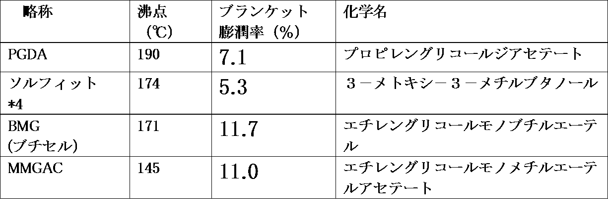
- organic solvent having a blanket swelling ratio of 5 to 20% as the organic solvent (D).
- organic solvents include those listed in the following table.
- the boiling point in the table is the boiling point at normal pressure
- the blanket swelling rate is measured by cutting out the blanket into 2 cm square, immersing the blanket in various organic solvents, and after 1 hour The sample was taken out from the solvent and weighed again to determine the rate of weight increase before and after immersion.
- propylene glycol diethylene glycol is used in that a printed pattern having excellent linearity and less prone to disconnection can be obtained both at the initial printing of the bezel pattern and at the time of more printing.
- Acetate (PDGA), 3-methoxy-3-methylbutanol (Solfit), etc. are preferred.
- the linearity is better when printing more than the first printing of the bezel pattern.
- the content of the organic solvent (D) in the conductive paste of the present invention is not particularly limited as long as the above effect can be obtained in the gravure offset printing method, but is preferably 5 to 30% by mass, Among these, 7 to 15% by mass is more preferable. Within this range, the paste viscosity becomes more appropriate, and in gravure offset printing, it is possible to form higher-definition printing patterns without causing pinhole defects at the corners of the image lines or at the intersections of the matrix. it can.
- the conductive paste of the present invention further contains at least one functional group selected from the group consisting of a phosphate group, a phosphate group, and a phosphate ester group in addition to the above-mentioned known and commonly used raw material components.
- An organic compound can be contained.
- the blanket In the formation of a conductive pattern from a conductive paste, when the above gravure offset printing method is employed, the blanket is required to have transferability from an intaglio and transferability to a substrate. In order to obtain sufficient transferability to the printing material, it is necessary to absorb the liquid component in the conductive paste at a certain ratio on the blanket surface. Insufficient absorption tends to cause delamination of the conductive paste layer during transfer to the substrate, and conversely if absorbed over a certain percentage, the conductive paste dries on the blanket surface, resulting in poor transfer to the substrate It is easy to cause.
- the conductive paste applied thereto is a paste having a paste viscosity of 100 Pa ⁇ s or less at a share rate of 1 s ⁇ 1 and a share rate of 100 s ⁇ 1.
- a viscosity of 2.0 to 5.0 Pa ⁇ s is preferable for obtaining a printed pattern having excellent linearity and having no defects such as disconnection.
- Such a suitable paste viscosity can be adjusted only by selecting the above-mentioned known and commonly used raw material components.
- at least one functional group selected from the group consisting of a phosphate group, a phosphate group, and a phosphate ester group is used.
- the organic compound (B) and the organic compound (C) are defined by an organic compound containing at least one functional group selected from the group consisting of a phosphate group, a phosphate group, and a phosphate ester group. Shall not be included.
- the phosphate group is a group represented by —H 2 PO 4 (P atom is pentavalent), and the phosphate group is at least one hydrogen atom in —H 2 PO 4 is an alkali metal ion or alkaline earth. It is a group in the form of a salt substituted with a metal ion.
- the phosphate group is a group in which at least one hydrogen atom in —H 2 PO 4 is substituted with an alkyl group or a phenyl group.
- an organic compound containing a phosphate group, an organic compound containing a phosphate group, and an organic compound containing a phosphate ester group are collectively abbreviated as a phosphate group-containing organic compound.
- organic compounds containing a phosphate group examples include polyalkylene glycol monophosphate, polyalkylene glycol monoalkyl ether monophosphate, perfluoroalkyl polyoxyalkylene phosphate, perfluoroalkylsulfonamide polyoxy Low molecular weight compounds such as alkylene phosphates, homopolymers of vinylphosphonic acid, acid phosphooxyethyl mono (meth) acrylate, acid phosphooxypropyl mono (meth) acrylate, and acid phosphoxypolyoxyalkylene glycol mono (meth) acrylate
- a polymer containing a phosphoric acid group such as a copolymer of the monomer and another comonomer may be mentioned as the polymer compound.
- an organic compound containing a phosphate group is illustrated as a specific example.
- an organic compound containing a phosphate group is not limited to an alkali metal hydroxide or an organic compound containing a phosphate group. It can be easily obtained by reacting an alkaline earth metal hydroxide, and an organic compound containing a phosphate ester group is obtained by dehydration condensation between an organic compound containing a phosphate chloride group and an alcohol. It is easy to obtain.
- phosphoric acid can be used in comparison with an organic compound containing a phosphate ester group in that it can have a lower viscosity and a lower volume resistivity in comparison with the same amount of nonvolatile content used.
- An organic compound containing a group or an organic compound containing a phosphate group is preferred.
- the low molecular weight compound is selected from, for example, EFKA series and Daiichi Kogyo Seiyaku Co., Ltd.'s PRISURF series manufactured by Ciba Specialty, while the high molecular compound is selected from, for example, the DISPERBYK (registered trademark) series manufactured by BYK Chemie. Can be used.
- a phosphate group-containing polymer having a number average molecular weight of 1,000 or more, in particular, a number average molecular weight of 1,000 to 10,000 is more conductive than the above-described low molecular compound at the same use amount. This is preferable because the effect of improving the fluidity of the conductive ink composition is high without impairing the properties.
- the usage-amount of the phosphoric acid group containing organic compound used by this invention is 0.00 per mass conversion total 100 parts of electroconductive metal particle (A), an organic compound (B), an organic compound (C), and an organic solvent (D). It is preferably 1 to 3 parts.
- various additives such as a dispersant, an antifoaming agent, a release agent, a leveling agent, and a plasticizer can be appropriately blended as necessary in addition to the above-described components.
- the conductive paste of the present invention can form a printing pattern by applying or printing on any substrate such as a plastic film, a ceramic film, a silicon wafer, glass or a metal plate by any method. it can.
- any substrate such as a plastic film, a ceramic film, a silicon wafer, glass or a metal plate by any method.
- the true value of the conductive paste of the present invention can be fully demonstrated when a PET film that cannot be exposed to high temperatures as a substrate to be printed when obtaining a conductive pattern or an ITO film using it as a support.
- Such a transparent conductive film is particularly useful in a transparent conductive film.
- the melting point of the conductive metal particles (A) is higher than the decomposition temperature of the organic compound (B). It is preferable not to contain an inorganic binder such as glass frit, which has a function of melting at less than that and binding the conductive metal particles (A) to the printing material.
- it is intended to fix the conductive metal particles (A) to the printing material exclusively based on the organic compound (B) and the organic compound (C). It is preferable that the content of the conductive metal particles (A) per se be reduced by the inclusion of, which makes it difficult to achieve excellent conductivity based on the conductive metal particles (A) itself, and also decreases the adhesion to the substrate. Absent.
- the conductive fine wiring pattern can be obtained by firing the printed pattern corresponding to the fine wiring pattern including the bezel pattern formed on the substrate in the gravure offset printing described above. In this firing, the removal of the organic solvent (D) contained in the paste and the occurrence of the curing reaction of the organic compound (B) and the organic compound (C) may be performed in this order, or these may be performed simultaneously. You can go.
- known conventional means such as heating with a heat source, irradiation with a xenon flash lamp, irradiation with ultra high frequency waves, irradiation with near infrared rays, irradiation with far infrared rays, etc.
- the above curing reaction may occur at 150 ° C. or lower.
- the printed material has a heat resistance such as glass.
- the conductive paste of the present invention the polyfunctional epoxy compound as the organic compound (B) and the polyfunctional as the organic compound (C) are used.
- a thermosetting conductive paste containing an epoxy compound and a curing catalyst can be used.
- the reaction is 150 ° C. or less, particularly 100 to 140 ° C.
- the conductive paste of the present invention contains an organic solvent (D), but the paste is thinned in the doctoring process, and volatilization proceeds from the surface even if it is less than the boiling point.
- the blanket since the blanket further absorbs the organic solvent (D) from the printing pattern itself transferred from the gravure plate, the organic solvent (D) in the printing pattern transferred from the blanket onto the substrate in the setting process.
- the content rate is reduced significantly. Therefore, the organic solvent (D) can be removed without heating to the boiling point or higher of the organic solvent (D) contained in the actually used conductive paste.
- thermosetting conductive paste suitable for the present invention becomes, for example, a cured film when heated at 100 to 140 ° C. for 30 to 5 minutes, and becomes a conductive pattern. Expresses conductivity.
- the preferred conductive paste of the present invention is characterized by the ceramic film, glass or metal plate. This is particularly prominent when a conductive pattern is formed on a non-heat-resistant printed material that has a lower heat resistance and is more likely to be thermally deformed than such a highly heat-resistant printed material.
- the conductive pattern in which the cured film of the preferred conductive paste of the present invention is formed on the non-heat-resistant printed material is preferably used as a conductive circuit formed on the non-heat-resistant printed material. it can.
- various printed materials provided with a conductive fine wiring pattern including a bezel pattern formed by a gravure offset printing method using the conductive paste of the present invention can be further connected as necessary as a conductive circuit.
- various electric parts and electronic parts can be obtained.
- the conductive fine wiring pattern obtained based on the conductive paste of the present invention is excellent in adhesion to a transparent conductive film such as a transparent ITO electrode.
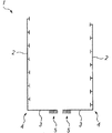
- a so-called bezel pattern 1 having an electrode part and a wiring part and formed along the edge of the display area of the touch panel is provided. Can be mentioned.
- the bezel pattern 1 is an aggregate of thin lines connected to, for example, a transparent electrode.
- the first thin line pattern 2 extending in a predetermined direction and the first thin line pattern 2 are substantially orthogonal to each other. It has a pair of substantially L-shaped wiring patterns 4, 4 composed of a second fine line pattern 3 extending from one end of the first fine line pattern 2 in the direction.
- An electrode pattern 5 is formed by a plurality of fine lines extending on the opposite side of the first fine line pattern 2 at the tip of the second fine line pattern 3, and a pair of substantially L-shaped wiring patterns 4, 4 are The electrode patterns 5 and 5 are arranged so as to face each other at a predetermined interval, and the first thin line patterns 2 and 2 are arranged substantially parallel to each other.
- the line widths of the first fine line pattern 2 and the second fine line pattern 3 can be set to 10 ⁇ m to 100 ⁇ m, for example.
- the electrode pattern 5 can be formed in a substantially rectangular region having a width of about 200 ⁇ m and a length of about 2000 ⁇ m, for example.
- the first fine line patterns 2 and 2 are thin lines in the Machine Direction (MD) direction
- the second fine line patterns 3 and 3 in the direction orthogonal to the first thin line patterns 3 and 3 are , Transverse ⁇ Direction (TD) direction thin line.
- MD Machine Direction
- TD Transverse ⁇ Direction
- the conductive paste of the present invention is not only a bezel pattern formed by connecting two or more linear recesses, such as a substantially L shape, a substantially inverted L shape, a combination thereof, or a substantially B shape, It can also be applied to obtain a conventional linear pattern.
- two or more optimal conductive pastes having different properties are prepared by forming a simple linear pattern and a complicated pattern such as an intersection of them, and printing the paste. There is no need to use different types of patterns according to the complexity of the power pattern, and one conductive paste of the present invention forms a complicated bezel pattern and other simple linear patterns at a time with one printing. Became possible.
- Examples of the final product include a touch panel take-out electrode, a display take-out electrode, electronic paper, a solar cell, and other wiring products.
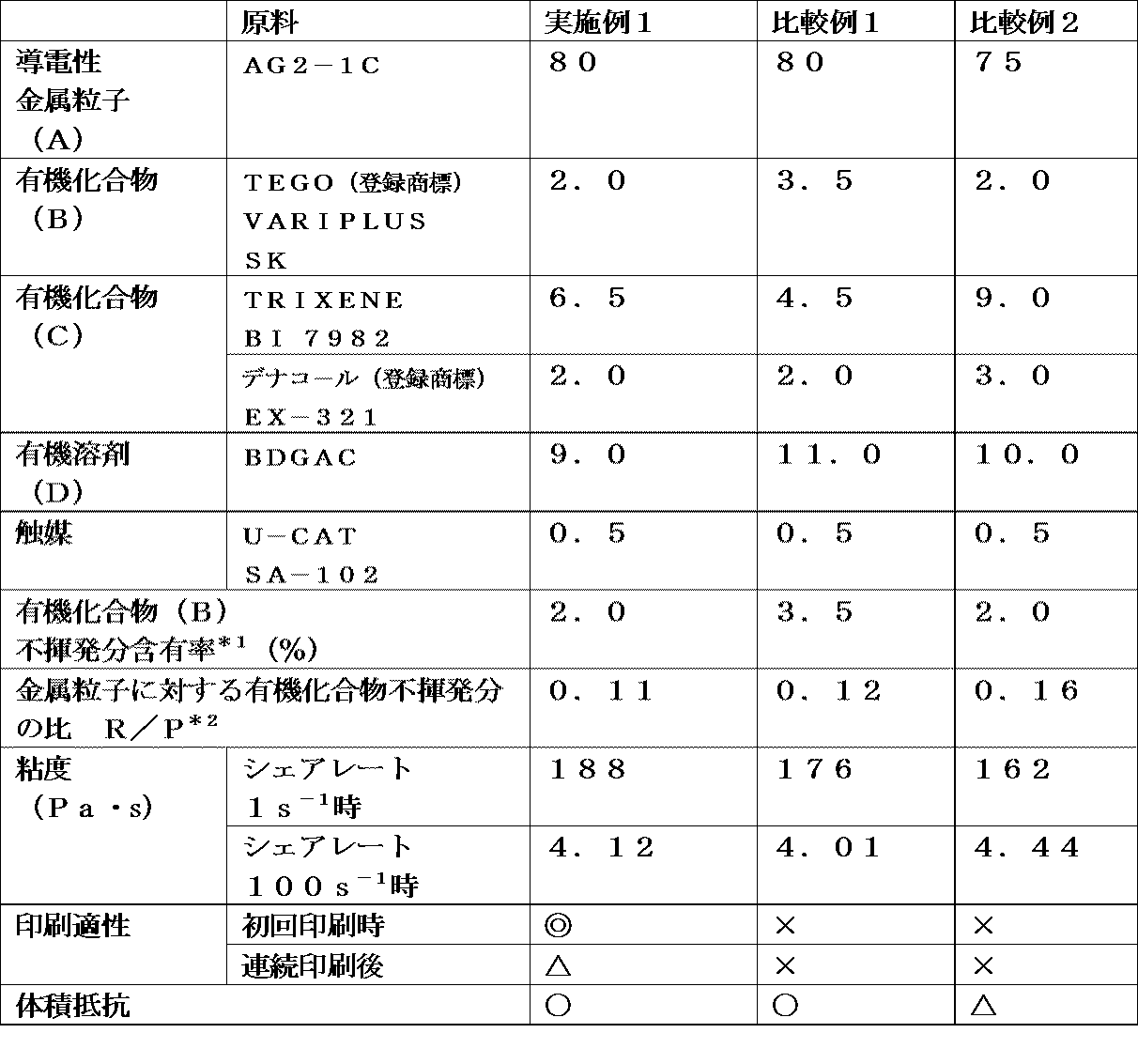
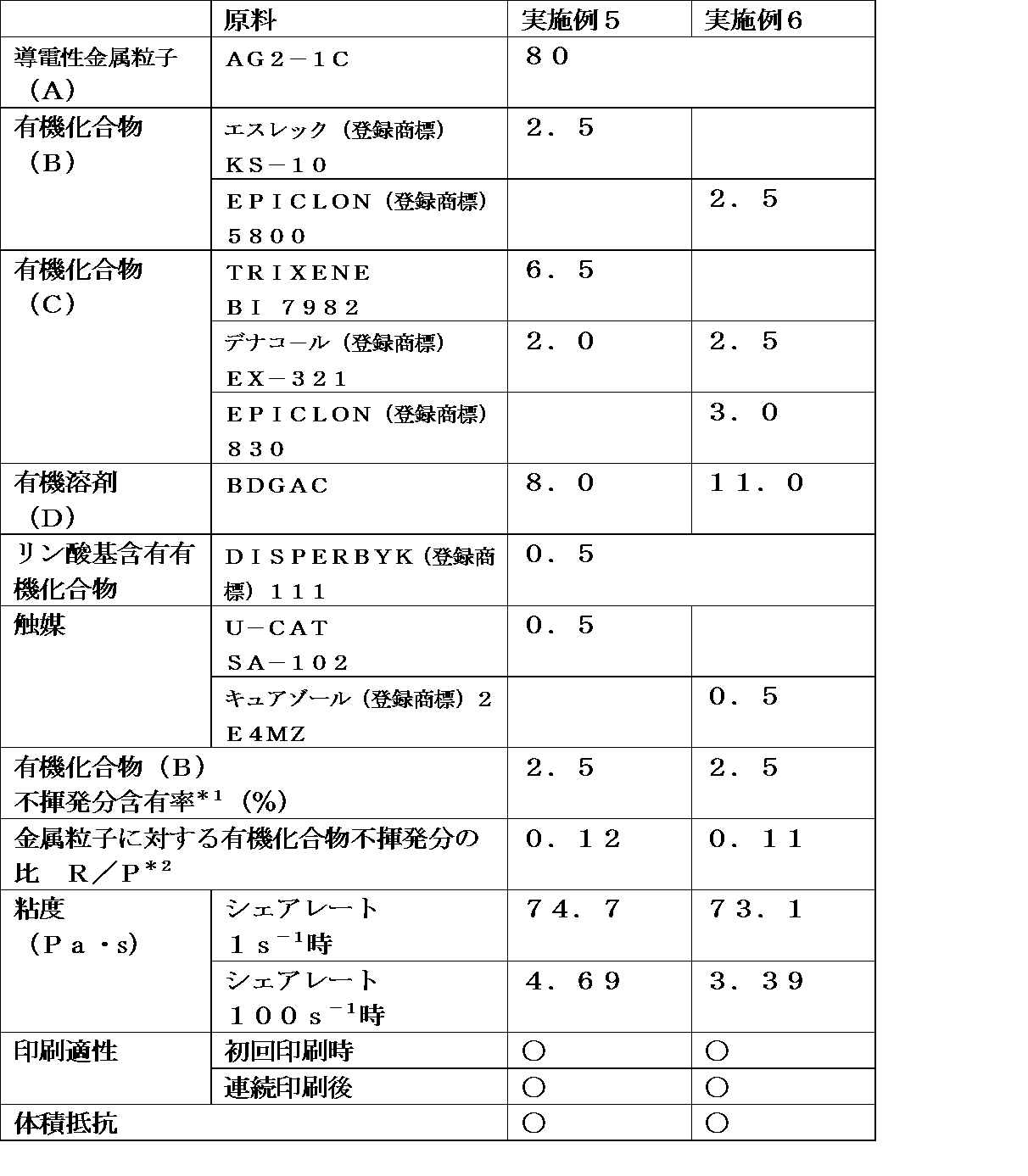
- each raw material so as to have the parts by mass shown in Table 1 are sufficiently mixed to prepare each conductive paste of the present invention as an example and each conventional conductive paste as a comparative example. did.
- a silicone blanket After inking each conductive paste with a doctor blade on a flat plate-shaped intaglio plate made of glass provided with grooves corresponding to the bezel pattern of FIG. 1 having a groove line width of 30 ⁇ m and a groove depth of 10 ⁇ m, a silicone blanket The desired pattern was transferred onto the blanket by being pressed and brought into contact with a cylinder around which was wound. Thereafter, the coating film on the blanket was pressed and transferred onto the ITO film surface of a sheet of transparent conductive film, which is a flat plate-like printed material, and printed, thereby producing a printed pattern having a line width of about 30 ⁇ m.
- a line corresponding to the TD direction of the printed bezel pattern having a width of about 30 ⁇ m was observed with a microscope, and the fine line reproducibility was evaluated as after the first printing according to the following criteria. .
- Printing was repeated, and the printed material after 100 printings (100 sheets) was also evaluated in the same manner as described above after continuous printing. Every 5 printings (every 5 sheets), hot air was blown to the silicone blanket with a dryer, and after confirming that the organic solvent that had permeated the blanket was volatilized, the next printing was performed.
- volume resistivity is a measure of conductivity.
- the electrically conductive paste of Example 6 since sufficient volume resistivity was not obtained on the said baking conditions, it replaced with the transparent conductive film, and it apply
- ESREC registered trademark
- KS-10 Polyvinyl acetal resin containing hydroxyl groups, manufactured by Sekisui Chemical Co., Ltd.
- EPICLON registered trademark
- 5800 A novolak type epoxy resin from DIC Corporation.
- TRIXENE BI 7982 A blocked polyisocyanate from Baxenden, whose blocking agent is 3,5-dimethylpyrazole.
- Denacol (registered trademark) EX-321 Trimethylolpropane polyglycidyl ether of Nagase ChemteX Corporation.
- Polylite (registered trademark) OD-X-2900 aromatic polyester polyol having an average molecular weight of 800 or more from DIC Corporation EPICLON (registered trademark) 830: bisphenol F diglycidyl ether type epoxy resin from DIC Corporation ⁇ Organic solvent (D)> ⁇ BDGAC: Diethylene glycol monobutyl ether acetate ⁇ phosphate group-containing compound> DISPERBYK (registered trademark) -111: a phosphate group-containing polymer having a number average molecular weight in the range of 1,000 to 10,000 from BYK Chemie. ⁇ Curing agent (curing catalyst)> U-CAT SA 102: DBU-octylate from San Apro Co., Ltd. Cureazole (registered trademark) 2E4MZ: 2-ethyl-4-methylimidazole from Shikoku Kasei Kogyo Co., Ltd.
- the non-volatile content (B) in the present invention is 1.0 to 3 in terms of mass with respect to the total of (A) to (D). 0.0% and in terms of the mass of the non-volatile content, the total usage amount of the organic compound (B) and the organic compound (C) is R, and the usage amount of the conductive metal particles (A) is P.
- Example 1 and Example 2 in the table contains an organic compound containing at least one functional group selected from the group consisting of a phosphate group, a phosphate group, and a phosphate ester group.
- the conductive paste of Example 2 having a viscosity at a rate of 1 s ⁇ 1 of not more than 100 Pa ⁇ s and a viscosity at a share rate of 100 s ⁇ 1 of 2.0 to 5.0 Pa ⁇ s is the above-described phosphate group. It can be seen that the printability after continuous printing is superior to the conductive paste of Example 1 which does not contain any organic compound and has a viscosity at a shear rate of 1 s -1 of more than 100 Pa ⁇ s.
- the conductive paste of each Example using a thermoplastic resin containing a hydroxyl group as the organic compound (B) is compared with the conductive paste of Example 6 using a polyfunctional epoxy compound as the organic compound (B). It can be fired at a lower temperature, and the energy required for firing can be reduced, and also for plastic films with poor heat resistance and transparent conductive films using it as a support, only a straight line is more complicated, It can be seen that a bezel pattern having conductivity can be formed.
- Each of the conductive pastes of the examples using the block polyisocyanate compound of the present invention can dissociate the blocking agent at a lower temperature than before, so that it has non-heat resistance such as a transparent conductive film or PET film. Even on the printed material, it was possible to form a conductive pattern comprising a cured film at low temperature in a short time without warping, and the obtained conductive pattern was sufficiently satisfactory in terms of conductivity and substrate adhesion.
- the conductive paste of the present invention can be used for forming conductive patterns of various electric parts and electronic parts.
Landscapes
- Chemical & Material Sciences (AREA)
- Engineering & Computer Science (AREA)
- Life Sciences & Earth Sciences (AREA)
- Materials Engineering (AREA)
- Wood Science & Technology (AREA)
- Organic Chemistry (AREA)
- Microelectronics & Electronic Packaging (AREA)
- Dispersion Chemistry (AREA)
- Manufacturing & Machinery (AREA)
- Chemical Kinetics & Catalysis (AREA)
- General Chemical & Material Sciences (AREA)
- Manufacturing Of Printed Wiring (AREA)
- Conductive Materials (AREA)
- Manufacturing Of Electric Cables (AREA)
- Printing Methods (AREA)
- Printing Plates And Materials Therefor (AREA)
- Parts Printed On Printed Circuit Boards (AREA)
Abstract
Description
エッチング法により導電パターンを形成する場合、各種金属膜を蒸着した基板上にフォトリソグラフィーによってパターン化されたレジスト膜を形成した後に、不要な蒸着金属膜を化学的あるいは電気化学的に溶解除去し、最後にレジスト膜を除去する必要がありその工程は非常に煩雑で量産性に乏しい。
そのため、例えば、上記特許文献1~3で用いられている導電性ペーストを、そこに記載された直線などの単純な形状の凹部を有するグラビア版を用いた場合には、直線性に優れ断線や短絡等の無い、意図した導電性パターンが得られるものの、一方で、特許文献1~3で用いられている導電性ペーストを、実際の電子部品に適用される様な、ベゼルパターンの様な複雑な凹部を有するグラビア版での印刷に用いると、上記した所期の性能が得られないという不具合が頻発するという欠点があった。
前記(B)不揮発分を、前記(A)~(D)の合計に対し、質量換算で1.0~3.0%とし、かつ、
不揮発分の質量換算で、前記有機化合物(B)と前記有機化合物(C)の合計使用量をR、前記導電性金属粒子(A)の使用量をPとした際の両者の質量比R/Pを、0.07~0.15とすることを特徴とする導電性ペーストことを特徴とする導電性ペーストを提供する。
また本発明は、ペーストが充填されるベゼルパターンを含む凹部が設けられたグラビア版と、ペーストをグラビア版の凹部に充填するドクターと、このグラビア版の凹部からペーストが受け渡されるブランケットと、このブランケットに対向させる様に被印刷物を供給して、両者を圧接させてブランケット上の微細配線パターンに対応するパターンを被印刷物に印刷し、次いで焼成を行う、グラビアオフセット印刷法による導電性パターンの形成方法において、前記ペーストとして、上記の導電性ペーストを用いることを特徴とする導電性パターンの形成方法を提供する。
更に本発明は、上記導電性ペーストで形成された導電性パターン印刷物を提供する。
前記(B)不揮発分を、前記(A)~(D)の合計に対し、質量換算で1.0~3.0%とし、かつ、不揮発分の質量換算で、前記有機化合物(B)と前記有機化合物(C)の合計使用量をR、前記導電性金属粒子(A)の使用量をPとした際の両者の質量比R/Pを、0.07~0.15とすることを特徴とする導電性ペーストである。
本発明で使用する導電性金属粒子(A)としては、公知の物がいずれも使用できる。例えば、ニッケル、銅、金、銀、アルミニウム、亜鉛、ニッケル、スズ、鉛、クロム、プラチナ、パラジウム、タングステン、モリブデン等、およびこれら2種以上の合金、混合体、あるいはこれら金属の化合物で良好な導電性を有するもの等が挙げられる。特に、銀粉は、安定した導電性を実現し易く、また熱伝導特性も良好なため好ましい。
本発明における導電性金属粒子(B)として銀粉を用いる場合、平均粒子径としてメジアン粒径(D50)が0.1~10μmである球状銀粉を用いることが好ましく、0.1~3μmであることがより好ましい。この範囲は、グラビアオフセット印刷法において、印刷機上での連続的に印刷した場合においても、トラブルが起こり難く安定的に良好な導電性パターンを得やすくなる。
本発明の導電性ペーストに用いる、50℃において固体であり常圧における沸点が300℃を超える有機化合物(B)は、当該有機化合物単独で良好な皮膜を形成でき、後記する様なブランケット上で良好な皮膜を形成すること、および当該ペ-スト皮膜がブランケットから被印刷物への完全転写することを可能にするものである。それ自体が50℃において固体であると共に、常圧における沸点が300℃を超え、後記する有機溶剤(D)に可溶で、焼成温度以下で溶融し流動しやすいものが好ましい。
本発明の導電性ペーストに用いる、50℃において液体であり常圧における沸点が300℃を超える有機化合物(C)は、なかでも、それ自体が50℃において液体であること、常圧における沸点が300℃を超えると共に、後記する有機溶剤(D)に可溶で、流動しやすいものが好ましい。
本発明で使用される有機化合物(B)及び有機化合物(C)は、グラビアオフセット印刷法に適する様に、通常は、溶媒に溶解し、かつ導電性金属粒子(A)はこれらの混合物に分散しペースト化した上で、被印刷物上に導電性ペーストの細線パターンを塗布したり印刷したりすることが必要となる。そのため、熱硬化性導電性ペースト構成する主剤及び硬化剤の選択に当たっては、溶媒への溶解性を考慮することが好ましい。

*2)KHネオケム(株)製品名
*3)東邦化学工業(株)製品名
回転式レオメータを用いて、25℃で、各導電性ペーストの1s-1及び100s-1のシェアレートでの各粘度を測定した。
実施例及び比較例の各導電性ペーストを用いて、下記の方法によりグラビアオフセット印刷を行い、ベゼルパターンを含む導電性パターンを、それぞれ作成した。
○: 線の直線性に優れ、断線箇所なし
△: 線の直線性に劣り、断線箇所なし
×: 線の直線性に劣り、断線箇所あり
アプリケーターを用いて透明導電性フィルム上(ITO膜面)に導電性ペーストを焼成後の膜厚が4μmになるように塗布し125℃で30分焼成させた。この焼成塗膜を用いて、ロレスタGP MCP-T610(三菱化学(株)製)で四端子法にて測定した。体積抵抗率は、導電性の高低の尺度である。尚、実施例6の導電性ペーストについては、上記焼成条件では充分な体積抵抗率が得られなかったため、透明導電性フィルムに代えてガラス板を用いて、塗布し180℃で30分焼成させた後に、上記と同様に評価した。
△: 5~10×10-4Ω・cm
×: 10×10-4Ω・cm以上
*2)不揮発分の質量換算で、前記有機化合物(B)と前記有機化合物(C)の合計使用量をR、前記導電性金属粒子(A)の使用量をPとした際の両者の質量比(R/P)(以下、同様。)。

<導電性金属粒子>
・AG2-1C:DOWAエレクトロニクス(株)の、平均粒径D50が0.8μmである銀粉。
<有機化合物(B)>
・TEGO(登録商標)VARIPLUS SK:エボニックデグサジャパン(株)の、ケトン-ホルムアルデヒド縮合体の水素添加物。水酸基を含有する。
・バイロン(登録商標)200:東洋紡績(株)の、水酸基を含有する熱可塑性ポリエステル樹脂。
・エスレック(登録商標)KS-10:積水化学工業(株)の、水酸基を含有するポリビニルアセタール樹脂。
・EPICLON(登録商標)5800:DIC(株)の、ノボラック型エポキシ樹脂。
<有機化合物(C)>
・TRIXENE BI 7982:バクセンデン社の、ブロック剤が3,5-ジメチルピラゾールのブロックポリイソシアネート。
・デナコ-ル(登録商標)EX-321:ナガセケムテックス(株)の、トリメチロールプロパンポリグリシジルエーテル。
・ポリライト(登録商標)OD-X-2900:DIC(株)の、平均分子量800以上の芳香族ポリエステルポリオール
・EPICLON(登録商標)830:DIC(株)の、ビスフェノールFジグリシジルエーテル型エポキシ樹脂
<有機溶剤(D)>
・BDGAC:ジエチレングリコールモノブチルエーテルアセテート
<リン酸基含有化合物>
・DISPERBYK(登録商標)-111:ビックケミー社の数平均分子量1,000~10,000の範囲にあるリン酸基含有ポリマー。
<硬化剤(硬化触媒)>
・U-CAT SA 102:サンアプロ(株)のDBU-オクチル酸塩。・キュアゾール(登録商標)2E4MZ:四国化成工業(株)の2-エチル-4-メチルイミダゾール
Claims (13)
- 導電性金属粒子(A)と、50℃において固体であり常圧における沸点が300℃を超える有機化合物(B)と、50℃において液体であり常圧における沸点が300℃を超える有機化合物(C)と、前記(B)及び(C)以外の、前記(B)及び(C)と反応性を有さない常圧における沸点170~300℃の有機溶剤(D)とを含有する、グラビアオフセット印刷法によるベゼルパターン印刷用導電性ペーストであって、
前記(B)不揮発分を、前記(A)~(D)の合計に対し、質量換算で1.0~3.0%とし、かつ、
不揮発分の質量換算で、前記有機化合物(B)と前記有機化合物(C)の合計使用量をR、前記導電性金属粒子(A)の使用量をPとした際の両者の質量比R/Pを、0.07~0.15とすることを特徴とする導電性ペースト。 - 前記有機溶剤(D)が、ブランケット膨潤率5~20%の有機溶剤である請求項1記載の導電性ペースト。
- シェアレート1s-1でのペースト粘度を100Pa・s以下、かつシェアレート100s-1でのペースト粘度を2.0~5.0Pa・sである請求項1または2記載の導電性ペースト。
- 更にリン酸基、リン酸塩基、リン酸エステル基からなる群から選ばれる少なくとも一つの官能基を含有する有機化合物を含有する請求項1または2記載の導電性ペースト。
- 前記有機化合物(B)が、水酸基を含有する熱可塑性樹脂を含む請求項1~4のいずれか一項に記載の導電性ペースト。
- 前記有機化合物(B)が、水酸基を含有する熱可塑性樹脂を含み、かつ、前記有機化合物(C)が、ブロックポリイソシアネート化合物と、多官能エポキシ化合物及び/又は高分子ポリオール化合物とを含む請求項1~5のいずれか一項に記載の導電性ペースト。
- 有機化合物(B)の分解温度以上、導電性金属粒子の融点未満で溶融する、前記導電性金属粒子を被印刷物へ結着させる無機結着剤を含有しない上記1~6のいずれか一項記載の導電性ペースト。
- ペーストが充填されるベゼルパターンを含む凹部が設けられたグラビア版と、ペーストをグラビア版の凹部に充填するドクターと、このグラビア版の凹部からペーストが受け渡されるブランケットと、このブランケットに対向させる様に被印刷物を供給して、両者を圧接させてブランケット上の微細配線パターンに対応するパターンを被印刷物に印刷し、次いで焼成を行う、グラビアオフセット印刷法による導電性パターンの形成方法において、前記ペーストとして、上記1~7のいずれか一項に記載の導電性ペーストを用いることを特徴とする導電性パターンの形成方法。
- グラビア版が、ベゼルパターンに対応する、線幅10~50μm、深さ5~20μmの凹部を含むグラビア版である請求項8記載の導電性パターンの形成方法。
- 被印刷物への印刷後に、有機溶剤(D)を吸収したブランケットを乾燥させる工程を含ませる請求項8または9記載の導電性パターンの形成方法。
- 焼成を150℃以下で行う請求項8~10のいずれか一項に記載の導電性パターンの形成方法。
- 被印刷物が、ポリエチレンテレフタレートフィルム又はそれを支持体とした透明導電性フィルムである請求項10記載の導電性パターンの形成方法。
- 請求項1~7のいずれか一項に記載の導電性ペーストで形成された導電性パターン印刷物。
Priority Applications (4)
| Application Number | Priority Date | Filing Date | Title |
|---|---|---|---|
| KR1020147030841A KR102116290B1 (ko) | 2013-01-30 | 2014-01-23 | 도전성 페이스트, 도전성 패턴의 형성 방법 및 도전성 패턴 인쇄물 |
| JP2014528723A JP5610112B1 (ja) | 2013-01-30 | 2014-01-23 | 導電性ペースト、導電性パターンの形成方法及び導電性パターン印刷物 |
| CN201480002338.9A CN104620684B (zh) | 2013-01-30 | 2014-01-23 | 导电性糊剂、导电性图案的形成方法及导电性图案印刷物 |
| US14/440,199 US9464198B2 (en) | 2013-01-30 | 2014-01-23 | Conductive paste, method for forming conductive pattern, and object with printed conductive pattern |
Applications Claiming Priority (2)
| Application Number | Priority Date | Filing Date | Title |
|---|---|---|---|
| JP2013015435 | 2013-01-30 | ||
| JP2013-015435 | 2013-01-30 |
Publications (1)
| Publication Number | Publication Date |
|---|---|
| WO2014119463A1 true WO2014119463A1 (ja) | 2014-08-07 |
Family
ID=51262177
Family Applications (1)
| Application Number | Title | Priority Date | Filing Date |
|---|---|---|---|
| PCT/JP2014/051367 Ceased WO2014119463A1 (ja) | 2013-01-30 | 2014-01-23 | 導電性ペースト、導電性パターンの形成方法及び導電性パターン印刷物 |
Country Status (6)
| Country | Link |
|---|---|
| US (1) | US9464198B2 (ja) |
| JP (1) | JP5610112B1 (ja) |
| KR (1) | KR102116290B1 (ja) |
| CN (1) | CN104620684B (ja) |
| TW (1) | TWI630625B (ja) |
| WO (1) | WO2014119463A1 (ja) |
Cited By (8)
| Publication number | Priority date | Publication date | Assignee | Title |
|---|---|---|---|---|
| WO2016084312A1 (ja) * | 2014-11-25 | 2016-06-02 | バンドー化学株式会社 | 導電性インク |
| JPWO2015046096A1 (ja) * | 2013-09-30 | 2017-03-09 | 東洋紡株式会社 | 導電性ペースト、導電性塗膜、導電回路、導電性積層体及びタッチパネル |
| JP2017061619A (ja) * | 2015-09-25 | 2017-03-30 | 三菱マテリアル株式会社 | オフセット印刷用のインキおよび塗膜の製造方法 |
| JP2017069198A (ja) * | 2015-09-29 | 2017-04-06 | 三ツ星ベルト株式会社 | 導電性ペースト及び導電膜付基板の製造方法 |
| CN106715613A (zh) * | 2014-09-18 | 2017-05-24 | E.I.内穆尔杜邦公司 | 可热成形的聚合物厚膜透明导体及其在电容式开关电路中的用途 |
| JP2019029340A (ja) * | 2017-07-28 | 2019-02-21 | 旭化成株式会社 | 導電性パターンの製造方法、及びプラズマ処理装置 |
| WO2023276690A1 (ja) * | 2021-07-02 | 2023-01-05 | 住友ベークライト株式会社 | 導電性樹脂組成物、高熱伝導性材料および半導体装置 |
| WO2024048627A1 (ja) * | 2022-09-01 | 2024-03-07 | タツタ電線株式会社 | 導電性塗料、及びシールド層を有する樹脂成形品の製造方法 |
Families Citing this family (6)
| Publication number | Priority date | Publication date | Assignee | Title |
|---|---|---|---|---|
| DE102015122034A1 (de) * | 2015-12-16 | 2017-06-22 | Ferro Gmbh | Thermoplastische Siebdruckpaste |
| EP3282453B1 (en) * | 2016-08-11 | 2023-07-12 | Henkel AG & Co. KGaA | Improved processing of polymer based inks and pastes |
| KR102238769B1 (ko) * | 2018-04-23 | 2021-04-09 | 삼성에스디아이 주식회사 | 전극 형성용 조성물 및 이로부터 제조된 전극과 태양전지 |
| KR102501588B1 (ko) * | 2018-08-08 | 2023-02-21 | 미쓰이금속광업주식회사 | 접합용 조성물, 그리고 도전체의 접합 구조 및 그의 제조 방법 |
| KR102722567B1 (ko) * | 2020-08-07 | 2024-10-29 | 도레이 카부시키가이샤 | 도전 페이스트, 프린트 배선판, 프린트 배선판의 제조방법, 프린트 회로판의 제조방법 |
| CN117580909A (zh) * | 2021-07-02 | 2024-02-20 | 住友电木株式会社 | 导电性树脂组合物、高导热性材料和半导体装置 |
Citations (6)
| Publication number | Priority date | Publication date | Assignee | Title |
|---|---|---|---|---|
| JPS62232467A (ja) * | 1986-04-01 | 1987-10-12 | Catalysts & Chem Ind Co Ltd | 導電性塗料組成物 |
| JPS62260877A (ja) * | 1986-04-17 | 1987-11-13 | Kawakami Toryo Kk | 異方導電性接着剤 |
| JPS62273273A (ja) * | 1986-05-20 | 1987-11-27 | Toho Chem Ind Co Ltd | 導電性塗布剤組成物 |
| JP2012038615A (ja) * | 2010-08-09 | 2012-02-23 | Dic Corp | 導電性銀ペースト、導電性パターンの形成方法及び導電性パターン印刷物 |
| JP2012038614A (ja) * | 2010-08-09 | 2012-02-23 | Dic Corp | 導電性銀ペースト、導電性パターンの形成方法及び導電性パターン印刷物 |
| JP2012041517A (ja) * | 2010-07-23 | 2012-03-01 | Taiyo Holdings Co Ltd | 導電性樹脂組成物 |
Family Cites Families (18)
| Publication number | Priority date | Publication date | Assignee | Title |
|---|---|---|---|---|
| US3948650A (en) * | 1972-05-31 | 1976-04-06 | Massachusetts Institute Of Technology | Composition and methods for preparing liquid-solid alloys for casting and casting methods employing the liquid-solid alloys |
| US3951651A (en) * | 1972-08-07 | 1976-04-20 | Massachusetts Institute Of Technology | Metal composition and methods for preparing liquid-solid alloy metal compositions and for casting the metal compositions |
| US3954455A (en) * | 1973-07-17 | 1976-05-04 | Massachusetts Institute Of Technology | Liquid-solid alloy composition |
| US3936298A (en) * | 1973-07-17 | 1976-02-03 | Massachusetts Institute Of Technology | Metal composition and methods for preparing liquid-solid alloy metal composition and for casting the metal compositions |
| US4108643A (en) * | 1976-09-22 | 1978-08-22 | Massachusetts Institute Of Technology | Method for forming high fraction solid metal compositions and composition therefor |
| US4345637A (en) * | 1977-11-21 | 1982-08-24 | Massachusetts Institute Of Technology | Method for forming high fraction solid compositions by die casting |
| JP2006260951A (ja) * | 2005-03-17 | 2006-09-28 | Osaka Univ | 導電性銅ペースト |
| US7892314B2 (en) * | 2005-08-26 | 2011-02-22 | Apex Advanced Technologies, Llc | Powder metal composition containing micronized deformable solids and methods of making and using the same |
| JP2007194122A (ja) * | 2006-01-20 | 2007-08-02 | Sumitomo Electric Ind Ltd | 導電性ペーストおよびそれを用いた配線基板 |
| JP2009245844A (ja) * | 2008-03-31 | 2009-10-22 | Sumitomo Rubber Ind Ltd | 導電性ペースト |
| JP4877303B2 (ja) * | 2008-10-01 | 2012-02-15 | Tdk株式会社 | 導電性ペーストおよび電子部品の製造方法 |
| JP2010159350A (ja) | 2009-01-08 | 2010-07-22 | Sumitomo Rubber Ind Ltd | インキ組成物およびそれを用いた凹版オフセット印刷法 |
| JP2010235780A (ja) | 2009-03-31 | 2010-10-21 | Mitsubishi Materials Corp | 印刷用インキ及び該インキを用いた塗膜の製造方法 |
| JP5611537B2 (ja) * | 2009-04-28 | 2014-10-22 | 日立化成株式会社 | 導電性接合材料、それを用いた接合方法、並びにそれによって接合された半導体装置 |
| JP2011037999A (ja) | 2009-08-12 | 2011-02-24 | Dic Corp | 導電性インキ及び導電性パターン形成方法 |
| JP5525335B2 (ja) * | 2010-05-31 | 2014-06-18 | 株式会社日立製作所 | 焼結銀ペースト材料及び半導体チップ接合方法 |
| WO2012014481A1 (ja) * | 2010-07-30 | 2012-02-02 | 太陽ホールディングス株式会社 | オフセット印刷用導電性ペースト |
| TWI532059B (zh) * | 2011-03-31 | 2016-05-01 | Taiyo Holdings Co Ltd | Conductive paste, conductive pattern formation method and conductive pattern |
-
2014
- 2014-01-23 JP JP2014528723A patent/JP5610112B1/ja active Active
- 2014-01-23 WO PCT/JP2014/051367 patent/WO2014119463A1/ja not_active Ceased
- 2014-01-23 KR KR1020147030841A patent/KR102116290B1/ko not_active Expired - Fee Related
- 2014-01-23 CN CN201480002338.9A patent/CN104620684B/zh not_active Expired - Fee Related
- 2014-01-23 US US14/440,199 patent/US9464198B2/en active Active
- 2014-01-24 TW TW103102787A patent/TWI630625B/zh not_active IP Right Cessation
Patent Citations (6)
| Publication number | Priority date | Publication date | Assignee | Title |
|---|---|---|---|---|
| JPS62232467A (ja) * | 1986-04-01 | 1987-10-12 | Catalysts & Chem Ind Co Ltd | 導電性塗料組成物 |
| JPS62260877A (ja) * | 1986-04-17 | 1987-11-13 | Kawakami Toryo Kk | 異方導電性接着剤 |
| JPS62273273A (ja) * | 1986-05-20 | 1987-11-27 | Toho Chem Ind Co Ltd | 導電性塗布剤組成物 |
| JP2012041517A (ja) * | 2010-07-23 | 2012-03-01 | Taiyo Holdings Co Ltd | 導電性樹脂組成物 |
| JP2012038615A (ja) * | 2010-08-09 | 2012-02-23 | Dic Corp | 導電性銀ペースト、導電性パターンの形成方法及び導電性パターン印刷物 |
| JP2012038614A (ja) * | 2010-08-09 | 2012-02-23 | Dic Corp | 導電性銀ペースト、導電性パターンの形成方法及び導電性パターン印刷物 |
Cited By (9)
| Publication number | Priority date | Publication date | Assignee | Title |
|---|---|---|---|---|
| JPWO2015046096A1 (ja) * | 2013-09-30 | 2017-03-09 | 東洋紡株式会社 | 導電性ペースト、導電性塗膜、導電回路、導電性積層体及びタッチパネル |
| CN106715613A (zh) * | 2014-09-18 | 2017-05-24 | E.I.内穆尔杜邦公司 | 可热成形的聚合物厚膜透明导体及其在电容式开关电路中的用途 |
| CN106715613B (zh) * | 2014-09-18 | 2020-02-18 | E.I.内穆尔杜邦公司 | 可热成形的聚合物厚膜透明导体及其在电容式开关电路中的用途 |
| WO2016084312A1 (ja) * | 2014-11-25 | 2016-06-02 | バンドー化学株式会社 | 導電性インク |
| JP2017061619A (ja) * | 2015-09-25 | 2017-03-30 | 三菱マテリアル株式会社 | オフセット印刷用のインキおよび塗膜の製造方法 |
| JP2017069198A (ja) * | 2015-09-29 | 2017-04-06 | 三ツ星ベルト株式会社 | 導電性ペースト及び導電膜付基板の製造方法 |
| JP2019029340A (ja) * | 2017-07-28 | 2019-02-21 | 旭化成株式会社 | 導電性パターンの製造方法、及びプラズマ処理装置 |
| WO2023276690A1 (ja) * | 2021-07-02 | 2023-01-05 | 住友ベークライト株式会社 | 導電性樹脂組成物、高熱伝導性材料および半導体装置 |
| WO2024048627A1 (ja) * | 2022-09-01 | 2024-03-07 | タツタ電線株式会社 | 導電性塗料、及びシールド層を有する樹脂成形品の製造方法 |
Also Published As
| Publication number | Publication date |
|---|---|
| US9464198B2 (en) | 2016-10-11 |
| CN104620684B (zh) | 2017-11-14 |
| TWI630625B (zh) | 2018-07-21 |
| JP5610112B1 (ja) | 2014-10-22 |
| US20150299478A1 (en) | 2015-10-22 |
| JPWO2014119463A1 (ja) | 2017-01-26 |
| TW201435916A (zh) | 2014-09-16 |
| KR102116290B1 (ko) | 2020-05-29 |
| KR20150114881A (ko) | 2015-10-13 |
| CN104620684A (zh) | 2015-05-13 |
Similar Documents
| Publication | Publication Date | Title |
|---|---|---|
| JP5610112B1 (ja) | 導電性ペースト、導電性パターンの形成方法及び導電性パターン印刷物 | |
| JP6031882B2 (ja) | 導電性インキ組成物、導電性パターンの製造方法及び導電性回路 | |
| JP5605516B2 (ja) | 導電性インキ組成物、導電性パターンの製造方法及び導電性回路 | |
| JP2015172103A (ja) | 導電性インキ組成物、導電性パターンの製造方法及び導電性回路 | |
| US11239004B2 (en) | Conductive resin composition and conductive structure using same | |
| JP5569732B2 (ja) | 導電性銀ペースト、導電性パターンの形成方法及び導電性パターン印刷物 | |
| CN115124880A (zh) | 一种半导体被动元件封装用绝缘油墨、制备方法及应用 | |
| JP5871201B2 (ja) | 導電性金属粒子の製造方法及び導電性ペースト | |
| JP6372689B2 (ja) | 導電性ペースト及び導電性パターンの形成方法 | |
| CN104661818A (zh) | 层叠体、导电性图案及电路 | |
| KR20130020367A (ko) | 은 페이스트 조성물 및 이를 이용한 전극의 형성방법 | |
| KR101726492B1 (ko) | 투명 전극 패턴의 제조 방법 | |
| US20220208411A1 (en) | Conductive resin composition, circuit board fabricated using conductive resin composition, and method of manufacturing circuit board | |
| JP5135818B2 (ja) | 印刷用インキ組成物及びその製造方法並びに該組成物を用いたプラズマディスプレイパネル用電極の形成方法及びその電極 | |
| KR20230067331A (ko) | 3차원 성형이 가능한 필름 히터 | |
| KR20170042090A (ko) | 나노 임프린트용 전도성 조성물 및 이의 제조 방법, 그리고 이를 이용하는 터치 패널의 제조 방법 |
Legal Events
| Date | Code | Title | Description |
|---|---|---|---|
| ENP | Entry into the national phase |
Ref document number: 2014528723 Country of ref document: JP Kind code of ref document: A |
|
| 121 | Ep: the epo has been informed by wipo that ep was designated in this application |
Ref document number: 14745758 Country of ref document: EP Kind code of ref document: A1 |
|
| ENP | Entry into the national phase |
Ref document number: 20147030841 Country of ref document: KR Kind code of ref document: A |
|
| WWE | Wipo information: entry into national phase |
Ref document number: 14440199 Country of ref document: US |
|
| NENP | Non-entry into the national phase |
Ref country code: DE |
|
| 122 | Ep: pct application non-entry in european phase |
Ref document number: 14745758 Country of ref document: EP Kind code of ref document: A1 |