WO2014118959A1 - 熱電変換素子および熱電変換モジュール - Google Patents
熱電変換素子および熱電変換モジュール Download PDFInfo
- Publication number
- WO2014118959A1 WO2014118959A1 PCT/JP2013/052271 JP2013052271W WO2014118959A1 WO 2014118959 A1 WO2014118959 A1 WO 2014118959A1 JP 2013052271 W JP2013052271 W JP 2013052271W WO 2014118959 A1 WO2014118959 A1 WO 2014118959A1
- Authority
- WO
- WIPO (PCT)
- Prior art keywords
- thermoelectric conversion
- lattice
- conversion module
- conversion element
- lattice structure
- Prior art date
- Legal status (The legal status is an assumption and is not a legal conclusion. Google has not performed a legal analysis and makes no representation as to the accuracy of the status listed.)
- Ceased
Links
Images







Classifications
-
- H—ELECTRICITY
- H10—SEMICONDUCTOR DEVICES; ELECTRIC SOLID-STATE DEVICES NOT OTHERWISE PROVIDED FOR
- H10N—ELECTRIC SOLID-STATE DEVICES NOT OTHERWISE PROVIDED FOR
- H10N10/00—Thermoelectric devices comprising a junction of dissimilar materials, i.e. devices exhibiting Seebeck or Peltier effects
- H10N10/80—Constructional details
- H10N10/85—Thermoelectric active materials
- H10N10/857—Thermoelectric active materials comprising compositions changing continuously or discontinuously inside the material
-
- H—ELECTRICITY
- H10—SEMICONDUCTOR DEVICES; ELECTRIC SOLID-STATE DEVICES NOT OTHERWISE PROVIDED FOR
- H10N—ELECTRIC SOLID-STATE DEVICES NOT OTHERWISE PROVIDED FOR
- H10N10/00—Thermoelectric devices comprising a junction of dissimilar materials, i.e. devices exhibiting Seebeck or Peltier effects
- H10N10/01—Manufacture or treatment
-
- H—ELECTRICITY
- H10—SEMICONDUCTOR DEVICES; ELECTRIC SOLID-STATE DEVICES NOT OTHERWISE PROVIDED FOR
- H10N—ELECTRIC SOLID-STATE DEVICES NOT OTHERWISE PROVIDED FOR
- H10N10/00—Thermoelectric devices comprising a junction of dissimilar materials, i.e. devices exhibiting Seebeck or Peltier effects
- H10N10/10—Thermoelectric devices comprising a junction of dissimilar materials, i.e. devices exhibiting Seebeck or Peltier effects operating with only the Peltier or Seebeck effects
- H10N10/17—Thermoelectric devices comprising a junction of dissimilar materials, i.e. devices exhibiting Seebeck or Peltier effects operating with only the Peltier or Seebeck effects characterised by the structure or configuration of the cell or thermocouple forming the device
-
- H—ELECTRICITY
- H10—SEMICONDUCTOR DEVICES; ELECTRIC SOLID-STATE DEVICES NOT OTHERWISE PROVIDED FOR
- H10N—ELECTRIC SOLID-STATE DEVICES NOT OTHERWISE PROVIDED FOR
- H10N10/00—Thermoelectric devices comprising a junction of dissimilar materials, i.e. devices exhibiting Seebeck or Peltier effects
-
- H—ELECTRICITY
- H10—SEMICONDUCTOR DEVICES; ELECTRIC SOLID-STATE DEVICES NOT OTHERWISE PROVIDED FOR
- H10N—ELECTRIC SOLID-STATE DEVICES NOT OTHERWISE PROVIDED FOR
- H10N10/00—Thermoelectric devices comprising a junction of dissimilar materials, i.e. devices exhibiting Seebeck or Peltier effects
- H10N10/10—Thermoelectric devices comprising a junction of dissimilar materials, i.e. devices exhibiting Seebeck or Peltier effects operating with only the Peltier or Seebeck effects
- H10N10/13—Thermoelectric devices comprising a junction of dissimilar materials, i.e. devices exhibiting Seebeck or Peltier effects operating with only the Peltier or Seebeck effects characterised by the heat-exchanging means at the junction
Definitions
- the present invention relates to a thermoelectric conversion element and a thermoelectric conversion module using a material having a nano-sized lattice or fine particles using artificial or self-organization.
- thermoelectric conversion element that has been known for a long time. In thermoelectric conversion, electricity is generated directly from a temperature difference without a drive unit, so there is less loss than a method of generating steam by generating heat from thermal power or nuclear heat and turning a turbine to generate electricity. Furthermore, it is environmentally friendly because it does not generate waste.
- thermoelectric conversion material that is relatively efficient at a temperature of 200 ° C. or lower.
- thermoelectric conversion material having a high conversion efficiency near room temperature such as Bi-Te
- Bi-Te thermoelectric conversion material having a high conversion efficiency near room temperature
- a cooling apparatus that does not use a refrigerant and has a low environmental load.
- thermoelectric conversion material system that is highly compatible with silicon is considered advantageous.
- thermoelectric conversion element As described above, a high-performance thermoelectric conversion element is required from the viewpoints of exhaust heat reuse and device cooling.
- thermoelectric conversion material The performance of such a thermoelectric conversion material is evaluated by a dimensionless figure of merit (ZT).
- thermoelectric conversion material ⁇ is electrical conductivity
- S is the Seebeck coefficient
- ⁇ thermal conductivity
- ZT is obtained by multiplying both sides of Equation (1) by temperature T.
- the formula (1) shows that a material having a high numerator Seebeck coefficient S and electrical conductivity ⁇ and a low denominator thermal conductivity ⁇ is desirable as the thermoelectric conversion material.
- Bi-Te-based materials have high conversion efficiency with a figure of merit ZT> 1, but both Bi and Te are expensive, and Te is extremely toxic. Therefore, Bi is used for mass production, cost reduction, and environmental load reduction. There is a need for a high-efficiency thermoelectric conversion material that replaces 2 Te 3 .
- Patent Documents 1 and 2 report thermoelectric conversion materials based on a silicide semiconductor or a full Heusler alloy Fe 2 VAl as a material system having a low environmental load.
- the silicide semiconductor is a material that becomes a semiconductor by a compound of silicon and metal, and can be constituted by a very inexpensive material system. Since Mg 2 Si is based on inexpensive Mg and Si, it is composed of a low-priced and non-toxic material system.
- full-Heusler alloys are composed of elements with low environmental impact and low cost such as Fe, V, Al, etc., so they do not use toxic rare metals like Bi-Te materials and are valuable for industrial applications. It is a certain material system. However, thermoelectric conversion characteristics exceeding the Bi-Te system have not been reached in a temperature range of 200 ° C. or lower, and further research and development are required in the future.
- thermoelectric conversion element As described above, although the performance of the thermoelectric conversion element varies greatly depending on the bulk properties of the material, it has also been reported that the size effect such as atomization can greatly improve the performance of the thermoelectric conversion element.
- the interface between the particles increases.
- the thermal conductivity can be greatly reduced.
- the figure of merit ZT of a thermoelectric conversion element is inversely proportional to the thermal conductivity, the reduction of the thermal conductivity is an extremely important design guideline for improving the performance of the thermoelectric conversion element.
- Non-Patent Document 1 also reports transition metal sulfides such as Fe and Ni as thermoelectric conversion materials that have a low environmental load and can be reduced in cost.
- transition metal sulfides such as Fe and Ni
- thermoelectric conversion materials that have a low environmental load and can be reduced in cost.
- JP 2004-253618 A Japanese Patent Laid-Open No. 2002-270907
- thermoelectric conversion element with high performance near room temperature that can be used for reuse of exhaust heat from circuits in a computer or cooling of a computer.
- thermoelectric conversion elements using toxic rare metals such as Bi-Te that have been put to practical use as thermoelectric conversion materials at relatively low temperatures (200 ° C or lower) are supplied to the market stably in large quantities at a low price. In general, the possibility of widespread use is low.
- An object of the present invention is to provide a high-performance thermoelectric conversion element having a high Seebeck coefficient and a low thermal conductivity even when a material system capable of reducing environmental load and cost is used, and thermoelectric conversion using the same To provide a module.
- two or more types of lattice points can be classified, different types of lattices are connected to each other, the number of different types of lattices is different, and the lattice structure is a nanoparticle or a semiconductor quantum dot It is set as the thermoelectric conversion element characterized by having the area
- thermoelectric conversion element is characterized in that the unit structure of the lattice is a complete graph, and the lattice structure is composed of an array of nanoparticles or semiconductor quantum dots and has regions of different conductivity types.
- the lattice structure which is a planar graph and a line graph of a lattice that is a sub-lattice structure of different types of lattices, has regions of different conductivity types configured by arranging nanoparticles or semiconductor quantum dots.
- the thermoelectric conversion element characterized by this.
- thermoelectric conversion module is formed using the thermoelectric conversion element.
- thermoelectric conversion element having a high Seebeck coefficient and low thermal conductivity and a thermoelectric conversion using the same even when a material system capable of reducing environmental load and cost is used. Modules can be provided.
- a triangular lattice is shown as an example of a complete graph.
- (b) is a diagram in which unit cells shown in (a) are periodically arranged in a two-dimensional direction
- FIG. It is a figure for demonstrating the procedure which makes a Tasaki lattice, and shows the cell structure connected by the end of amplitude 0.
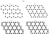
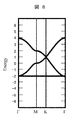
- FIG. It is a figure for demonstrating how to make a line graph, (a) is a hexagonal lattice, (b) is the 1st step which changes from a hexagonal lattice to a kagome lattice, (c) is the 2nd step which changes from a hexagonal lattice to a kagome lattice. , (D) shows a kagome lattice. It is a band figure of a Kagome lattice.
- thermoelectric conversion element which concerns on 1st Example of this invention
- a perspective view for demonstrating the formation process of the fine particle thermoelectric element which comprises the thermoelectric conversion element which concerns on 1st Example of this invention, and shows the process of apply
- a perspective view for demonstrating the formation process of the fine particle thermoelectric element which comprises the thermoelectric conversion element which concerns on the 1st Example of this invention, and shows the lithography process with respect to the resist film formed by apply
- thermoelectric conversion element which concerns on 1st Example of this invention
- the process of doping the metal element is shown.
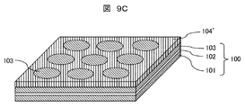
- FIG. 9A to FIG. A state in which a plurality of P-type regions are formed is shown. It is a perspective view for demonstrating the process of manufacturing the thermoelectric conversion module which concerns on 1st Example of this invention, and several N type area
- thermoelectric conversion module which concerns on 1st Example of this invention
- mold on an SOI substrate are carried out by the process shown to FIG. 9A to FIG. 9E.
- a state in which an n-type region is formed is shown.
- region are partially connected in series, and many extraction electrodes are formed in the circumference
- thermoelectric conversion module It is a perspective view for demonstrating the conventional thermoelectric conversion module, and several upper electrode shifts
- thermoelectromotive force strongly depends on the electronic state of the substance, and a material with a sharp change in the state density near the Fermi level is preferable. A material having a large change in density of states needs to be in a localized electronic state. Therefore, a material system in which electrons of d orbital such as transition metals contribute to an electronic state in the vicinity of Fermi level is one candidate. Become.
- transition metals examples include iron (Fe) and manganese (Mn). If the material system in which the state derived from 3d of Fe is a material system having a material system in the vicinity of the Fermi level as a parent phase, the amount of crustal reserves is large, and a thermoelectric conversion material with a low environmental load can be produced. Therefore, it is desirable to use silicide semiconductor fine particles such as Mn 4 Si 7 and ⁇ -FeSi 2 together with materials such as Si and Ge.
- a material system such as 68 , Ir 4 Ge 5 , or Co 2 Si 3 may be used.
- Bi-Te materials that are difficult to fabricate on semiconductor devices such as Si, and pyrite-structured FeS 2 , AuSb 2 , CaC 2 , CoS 2 , MnS 2 , NiS 2 , NiSe 2 , OsS 2 , OsTe 2 , PdAs 2 , PtAs 2 , PtBi 2 , RhSe 2 , RuS 2 , oxides, Heusler alloys, clathrate materials, or the like may be used.
- an artificial lattice having a possibility of forming a flat band is considered as a preferable shape as the artificial lattice.
- a flat band is a band structure in which the energy dispersion of electrons has almost no wave number dependency. If such a band structure can be artificially produced, a large thermoelectromotive force can be expected.
- the existence of many grids with flat bands has been clarified by Lieb, Tazaki, Mielke et al. These three lattice structures are described below.
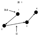
- FIG. 1 shows an example of a graph.
- FIG. 1 it is possible to define how the lattices are connected by a set of vertices (black circles) and sides (lines connecting the vertices).
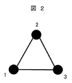
- FIG. 2 shows a triangular lattice which is an example of a complete graph. A complete graph is called when all vertex sets are connected to all vertices by edges as shown in FIG.
- the shape of the dimensional artificial lattice can be defined by periodically arranging the graph as a unit.
- the design guideline of the actual artificial lattice can be obtained by setting the vertex part in the graph to the position where the fine particles or quantum dots are arranged and making the side correspond to the semiconductor fine wire, metal fine wire, or the junction between the fine particles where electrons can jump. .
- FIG. 3 is an example of a Lieb type lattice.
- FIG. 8C is a diagram in which the unit cells are periodically arranged in the one-dimensional direction.
- the leap type is a lattice composed of two sublattices A and B as shown in FIG. 3A, and has a structure with an edge between A and B. Further, the number of grid points of A and B is different.
- FIG. 3 shows an example in which the ratio of grid points (A: B) is 2: 1.
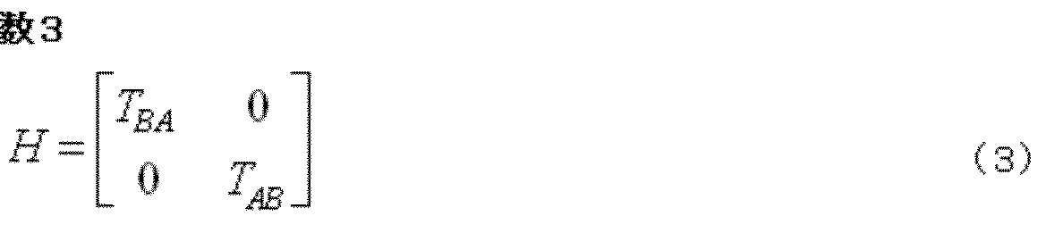
- the vertices B at the four corners are each counted as 1 ⁇ 4, for a total of one point, and the four sides A are counted as 1 ⁇ 2, for a total of two points. Therefore, it can also be written as shown in FIG. Considering a Hamiltonian with such a lattice structure,
- T BA and T AB are jump integrations from A to B sites, and T AB is a “number of A sites” ⁇ “number of B sites” matrix.
- FIG. 3B It may be an arranged two-dimensional lattice (FIG. 3B) or a one-dimensional lattice (FIG. 3C) in which the shapes shown in FIG.
- FIG. 3C is periodic only in the one-dimensional direction, and therefore, all B sites at the four corners do not appear as in FIG. 3A, but there are no sites in the upper row.
- the dotted line portion is described.
- Example 2 of desirable shape of artificial lattice Tasaki type
- the Tasaki type has a feature that a unit cell is a complete graph. In the Tasaki lattice, it is important to select the basic cell, and even if the localized eigenstate generated in the unit cell is connected to the cell, the flat band is not changed. It is a grid that is made.
- the triangular lattice shown in FIG. 2 is an example of a complete graph, and all lattice points are connected by edges.
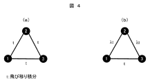
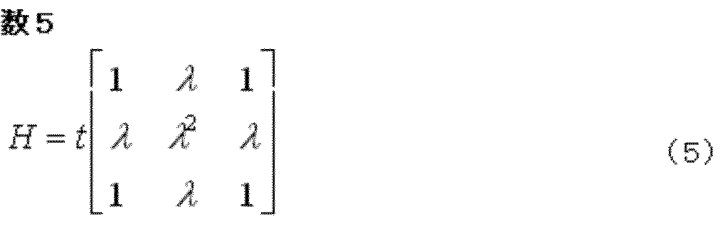
- the Hamiltonian of a triangular unit cell as shown in FIG. 4A has a jump integral value of 1 and on-site energy of 1.
- This eigenvalue is a zero eigenvalue that is degenerate twice.
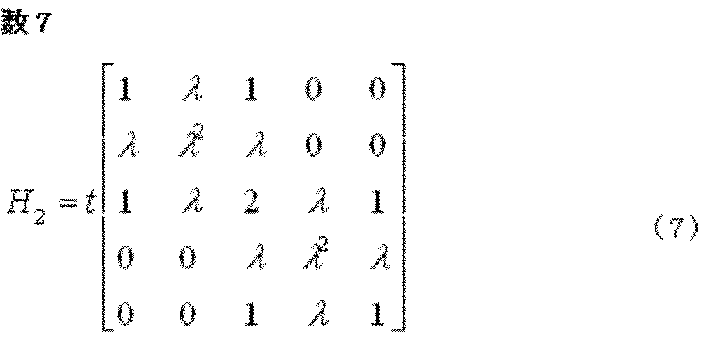
- a lattice having a flat band can be made by maintaining a localized eigenstate by successfully connecting such eigenstates having zero eigenstates.
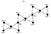
- the procedure for creating a Tazaki-type lattice will first focus on the eigenstates having zero eigenvalues of unit cells that form a complete graph.
- FIG. 6 is a diagram for explaining a procedure for forming a Tazaki lattice, and shows a cell structure connected at the end of zero amplitude. If a connected cell having such a state where the amplitude at the end is 0 is formed, even if the sites where the amplitude is 0 are connected to each other, the localized state maintains the shape and the eigenvalue of the zero eigenvalue of all Hamiltonians is maintained. It can be confirmed that it continues to be a function.
- This localized eigenstate overlaps with the localized eigenstate spreading in the adjacent unit cell, and the flat band eigenstate is a non-orthogonal localized state that is degenerate in the same manner as the leap type.
- a lattice having a flat band can be manufactured. Therefore, a flat band can be realized by using a lattice formed by connecting unit cells that are complete graphs, and a lattice having a complete graph-shaped unit cell having a localized state is one of desirable shapes. .
- Examples of desired shape of the artificial lattice 3 Miruke type Miruke type grating and a planar graph, a line graph L G when the gratings with the graph G in the two AB sublattice of the lattice of the lattice and B that A structure It has the feature that it is a lattice.
- FIG. 7A shows a graph G h having a hexagonal lattice shape. This hexagonal lattice can be regarded as a structure in which the same type of lattice forms a sub-lattice.
- FIG. 7B first stage. If the side of G h on which the newly arranged different vertices are connected is connected by the vertex of one G h , the two sides are connected by a new side as shown in FIG. Stage). As shown in FIG. 7 (d), a new chart made by the series of operations is referred to as "line graph of G h", expressed as L G. From the relationship between FIG. 7A and FIG.
- the line graph of the hexagonal lattice shape is a Kagome lattice (a pattern in which atoms and the like are arranged in a lattice pattern in the crystal lattice). . Therefore, it is understood that the kagome lattice is a kind of Mirke lattice. Further, in the Mirke type lattice having the above structure, a flat band exists when the Hamiltonian is solved using the tight binding model.
- an artificial lattice shape having the structure
- the lattice can be formed by arranging nanoparticles or quantum dots.
- An artificial lattice may be made by arranging the nanoparticles themselves at lattice points.
- a region where semiconductor thin wires intersect acts as a quantum dot, and such a quantum dot region may be used as a lattice point.
- the lattice structure may be formed by using electron beam lithography. Further, self-organization of fine particles may be used. Regardless of which method is used, the crystal structure of the thermoelectric conversion material can be easily confirmed by X-ray diffraction (XRD).
- a lattice image can be observed with an electron microscope such as TEM (Transmission-Electron-Miroscope) or a single crystal or polycrystal structure can be confirmed from a spot pattern or ring pattern in an electron beam diffraction image.
- the composition distribution of the sample is measured using techniques such as EPMA (Electron Probe Probe MicroAnalyser) such as EDX (Energy Dispersive X-ray Spectroscopy), SIMS (Secondary Ionization Mass Mass Spectrometer), X-ray photoelectron spectroscopy, ICP (Inductively Coupled Plasma). I can confirm.
- Information on the state density of the material can be confirmed by ultraviolet photoelectron spectroscopy or X-ray photoelectron spectroscopy.
- the electrical conductivity and carrier density can be confirmed by electrical measurement using the four-terminal method and Hall effect measurement.
- the Seebeck coefficient can be confirmed by giving a temperature difference to both ends of the sample and measuring the voltage difference between both ends.
- the thermal conductivity can be confirmed by a laser flash method.
- the arrangement of the artificial lattice can be easily confirmed by SEM (Scanning / Electron / Miroscope) or TEM.
- Example preparation example 1 A thin film having a thickness of about 300 nm is formed on a Si substrate having a thermal oxide film by sputtering using a mixed target having a composition of Si and Mn of 3: 1. Time heat treatment was performed. Thereafter, it was immersed in a 1 mol / l potassium hydroxide aqueous solution for about 20 seconds. As a result of measuring the surface roughness with an atomic force microscope (AFM), the surface roughness increased. This is because the Si region was dissolved by immersion in potassium hydroxide and MnSi 1.75 was exposed on the surface. As a result of X-ray diffraction analysis of the thin film, a peak of Mn 4 Si 7 crystal could be observed. Further, when the particle diameter was measured using AFM and TEM, it was confirmed that fine particles having a diameter of 5 to 20 nm were produced.
- AFM atomic force microscope
- sample preparation example 2 An SOI (Silicon on insulator) substrate having an Si single crystal having a thickness of 100 nm on an Si substrate having an oxide film is implanted with Mn by an ion implantation method and heat-treated in a nitrogen atmosphere at 700 ° C. for 1 hour. Went. Thereafter, when the particle size was measured using TEM, fine particles of 5 to 10 nm were observed, and a thin film in which fine particles of Mn 4 Si 7 crystals using Si as a host were distributed was prepared from electron diffraction.
- SOI Silicon on insulator
- Example preparation example 3 A positive electron beam lithography resist film was formed on an SOI substrate having a Si single crystal layer of about 20 nm by spin coating, and the resist film was patterned so as to have a kagome lattice structure. Thereafter, post-baking was performed at 150 ° C., followed by immersion in HF having a concentration of about 5% for several seconds, followed by pure rinsing and immersion in a 1 mol / l potassium hydroxide aqueous solution for about 2 minutes. Thereafter, the resist film was removed, and an artificial lattice structure of Si having a kagome lattice structure was obtained.
- Example preparation example 4 A negative resist film for electron beam lithography was formed on an SOI substrate having a Si single crystal layer of about 20 nm by spin coating, and the region from which the resist of the kagome lattice structure was removed was patterned. Thereafter, an Mn metal film having a thickness of 10 nm was laminated on the sample with the resist film by a sputtering apparatus, and then lifted off to obtain an SOI substrate on which the Mn metal film having a kagome lattice structure was firmly laminated. Thereafter, heat treatment was performed for 1 hour in a nitrogen atmosphere at 700 ° C. The sample was immersed in a 1 mol / l potassium hydroxide aqueous solution for about 2 minutes. When the thin film was confirmed by SEM, a kagome lattice structure was obtained, and when confirmed by XRD, the thin film having the kagome lattice structure was a Mn 4 Si 7 crystal film.
- Example measurement example 1 A temperature difference between room temperature and 20 ° C. was made on the samples prepared in Preparation Example 3 and Preparation Example 4, and the Seebeck coefficient was measured. As a result, high Seebeck coefficients of 350 ⁇ V / K and 300 ⁇ V / K were obtained, respectively. As a result, it was confirmed that the thin film having the kagome lattice structure expresses a high Seebeck coefficient and is a material system having a high thermoelectromotive force.
- a vacuum vapor deposition method such as molecular beam epitaxy other than the above, or chemical vapor deposition using a transition metal complex or the like may be used.
- Fine particles and nanowires may be artificially produced using a general chemical vapor deposition (CVD) method, and then dispersed and a lattice structure may be produced using a technique such as self-organization.
- CVD general chemical vapor deposition
- a fine particle may be produced by heating and refluxing a molecule containing Si or a transition metal complex in an organic solvent and thermally decomposing the molecule in the organic solvent.
- Si and Mn 4 Si 7 were described as the materials having a kagome lattice, but in addition, TiSi 2 , TiGe 2 , V 17 Ge 31 , Cr 11 Ge 19 , Mo 9 Ge 16 , and full A material system doped with a material system such as Heusler alloy, half-Heusler alloy, or ⁇ -FeSi 2 as a base material may be used.
- an artificial band structure can be constructed, the electronic state at the Fermi level can be modulated, and a high thermoelectromotive force can be realized.
- materials that are inexpensive and less likely to be depleted the cost can be greatly reduced as compared with the Bi-Te system.
- FIGS. 9A to 12B A first embodiment of the present invention will be described with reference to FIGS. 9A to 12B. Note that matters described in the column of the embodiment for carrying out the invention but not described in the present embodiment can be applied to the present embodiment unless there are special circumstances.
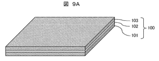
- FIG. 9A shows a step of preparing the SOI substrate 100 in which the SiO 2 layer 102 and the single crystal Si layer 103 are sequentially stacked on the Si substrate 101.
- the thickness of the Si layer 103 was 20 nm.
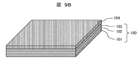
- a positive resist for electron beam lithography was applied to the surface of the Si layer 103 of the SOI substrate 100 to form a resist film 104 (FIG. 9B).
- the resist film 104 was patterned by electron beam lithography to obtain a resist film 104 ′ having a plurality of openings (FIG. 9C).
- the Si layer 103 is exposed in the opening (there may be an insulating film such as SiO 2 on the surface of the Si layer 103).
- a desired metal element here, Mn
- the carrier type can be changed by introducing Fe, Cr or the like having a different valence electron number.
- a heat treatment was performed at 700 ° C. to form a silicide layer 130 in the region doped with the metal element, thereby forming a fine particle thermoelectric element (FIG. 9E).
- thermoelectric conversion element can be manufactured by making an N-type region and a P-type region separately and connecting these regions in series. Further, although the present embodiment has been described as fine particles, it may be constituted by quantum dots. Further, the resistivity of the silicide layer can be 10 ⁇ m to 1000 ⁇ m.
- the thermoelectric conversion element using the fine particle artificial lattice system according to the present example has a dimensionless figure of merit ZT exceeding 3 near room temperature, compared with the case of using the conventional Bi 2 Te 3 (ZT ⁇ 1). It is possible to improve the thermoelectric conversion efficiency by 50% to 100%.
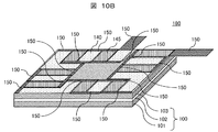
- FIG. 10A is a perspective view for explaining a process of manufacturing the thermoelectric conversion module according to the present embodiment, and a plurality of N-type regions 140 and a plurality of (( Here, a state is shown in which P-type regions 145 (the same number as the N-type regions) are formed.
- the detailed configuration of the N-type region 140 and the P-type region 145 is the same as that in FIG. 9E as shown in the enlarged view on the left side of FIG. 10A.
- an electrode that connects all of the plurality of N-type regions and the plurality of P-type regions in series and two extraction electrodes 150 are formed (FIG. 10B).
- an electrode manufacturing method ion implantation, vacuum deposition, or the like is used. Thereby, an in-plane temperature control type thermoelectric conversion module can be manufactured.
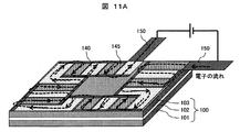
- FIG. 11A is a perspective view for explaining the flow of electrons when a voltage is applied to the thermoelectric conversion module shown in FIG. 10B.
- FIG. 11B is a perspective view for explaining a temperature change of the thermoelectric conversion module when a voltage is applied to the thermoelectric conversion module as shown in FIG.
- thermoelectric conversion module By flowing electrons in this way, as shown in FIG. 11B, the central region of the thermoelectric conversion module which is the temperature controllable portion 160 is cooled, and the ambient temperature rises. That is, the in-plane temperature can be controlled by the thermoelectric conversion module.
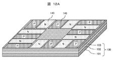
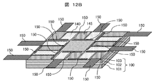
- FIG. 12A is a perspective view for explaining a process of manufacturing the thermoelectric conversion module according to the present embodiment, and a plurality of N-type regions 140 and a plurality of (( Here, a state is shown in which P-type regions 145 (the same number as the N-type regions) are formed.
- the detailed configuration of the N-type region 140 and the P-type region 145 is the same as that in FIG. 9E as shown in the enlarged view on the left side of FIG. 10A.
- an electrode that partially connects a plurality of N-type regions and a plurality of P-type regions in series and a plurality of extraction electrodes 150 are formed (FIG. 12B). Since the voltage applied for each region can be changed, an in-plane temperature control type thermoelectric conversion module capable of more precise temperature control than the thermoelectric conversion module shown in FIG. 10B can be manufactured.
- thermoelectric conversion element having a high Seebeck coefficient and low thermal conductivity is used. It is possible to provide a thermoelectric conversion module.
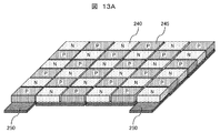
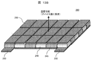
- FIG. 13A and 13B are perspective views for explaining a conventional thermoelectric conversion module.
- FIG. 13A shows a state in which a plurality of N layers 240 and a plurality of P layers 245 are arranged on a plurality of lower electrodes 250.
- FIG. 13B shows a state in which the plurality of upper electrodes are arranged so as to be shifted from the plurality of lower electrodes so that all of the plurality of N layers 240 and the plurality of P layers 245 shown in FIG. 13A are all connected in series.
- the thermoelectric conversion module for example, when the cathode side of the power source is connected to the extraction electrode 250 on the right side of the lower end of the lower electrode with respect to the N layer and the P layer connected in series, the extraction electrode passes through the N layer.
- the conventional thermoelectric conversion module 280 is a surface direct temperature control type thermoelectric conversion module having a temperature gradient in a direction perpendicular to the device surface.
- Example 1 a configuration in which the in-plane temperature control type thermoelectric conversion module shown in Example 1 and the above-described conventional in-plane temperature control type thermoelectric conversion module are combined will be described.
- FIG. 14A is a perspective view showing a state immediately before the assembly of the thermoelectric conversion module according to the second embodiment of the present invention.
- This thermoelectric conversion module includes a conventional surface temperature control type thermoelectric conversion module 280, a layer 170 for transferring heat only to the outer periphery of the intermediate device, and the in-plane temperature control type thermoelectric conversion module of Example 1 shown in FIG. 10B. 180 (intermediate device), a layer 170 for transferring heat only to the outer periphery of the intermediate device, and a conventional surface temperature control type thermoelectric conversion module 280 are included as components.
- FIG. 14B is a perspective view of the thermoelectric conversion module according to the second embodiment of the present invention. By setting it as this structure, it can be set as the thermoelectric conversion module which can lower the temperature of center part further.
- thermoelectric device using a high-performance thermoelectric conversion element having a high Seebeck coefficient and low thermal conductivity.
- a conversion module can be provided. Further, by combining with a conventional surface temperature control type thermoelectric conversion module, the temperature of the central portion can be further lowered.
- Si or Ge and their metal compounds are made into nano-sized fine particles or quantum dots using lithography or self-organization technology, and some or all of the fine particles or quantum dots are regularly arranged. Can improve the density of states and reduce the thermal conductivity.
- an artificial lattice is formed, and a band structure in which the energy dispersion of electrons, such as a flat band, has almost no wave number dependency is created by a lattice of artificial fine particles, and the state density is huge. It is characterized by making a system.
- thermoelectric conversion material in which nanoparticles composed mainly of Si, SiGe, silicide semiconductor FeSi, MnSi 1.7 , ⁇ -FeSi 2 or Mg 2 Si are dispersed in a host material or a regular artificial lattice is formed. It is. By arranging nano-sized particles on an artificial lattice, a region having a high energy potential and a region having a low energy potential are formed, and a region to be a quantum dot in which electrons are confined is formed. Electrons can move between adjacent quantum dots. By creating an artificial lattice shape with a specific shape, the electron energy band includes a flat band structure in which the energy dispersion of electrons has little wave number dependence.
- a semiconductor superlattice thermoelectric conversion material characterized by the above.
- the present invention it is possible to improve the density of states and increase the Seebeck coefficient by atomizing a semiconductor material.
- the nano-particles are dispersed or have a regular structure, and the presence of a larger number of particle interfaces than a normal bulk material can greatly reduce the thermal conductivity.
- an artificial lattice such as a kagome lattice (a pattern in which atoms etc. are arranged in a lattice pattern in a crystal lattice)
- a system in which fine particles are regarded as artificial atoms can be produced.
- the band structure By controlling the band structure, the state density of the whole system can be changed and a higher thermoelectromotive force can be realized.
- this invention is not limited to the above-mentioned Example, Various modifications are included.
- the above-described embodiments have been described in detail for easy understanding of the present invention, and are not necessarily limited to those having all the configurations described.
- a part of the configuration of a certain embodiment can be replaced with the configuration of another embodiment, and the configuration of another embodiment can be added to the configuration of a certain embodiment.
- thermoelectric conversion module 100 ... SOI substrate, 101 ... Si substrate, 102 ... SiO 2 layer, 103 ... Si layer, 104, 104 '... resist film, 120 ... Ion implantation, 130 ... silicide layer, 140 ... N-type region, 145 ... P-type region, 150 ... electrodes, 160 ... temperature controllable part, 170 ... a layer for transferring heat only to the outer periphery of the intermediate device, 180 ... in-plane temperature control type thermoelectric conversion module, 240 ... N layer, 245 ... P layer, 250 ... electrodes, 280 ... Conventional thermoelectric conversion module.
Landscapes
- Engineering & Computer Science (AREA)
- Manufacturing & Machinery (AREA)
- Silicon Compounds (AREA)
Abstract
Description

1.Qを有限集合、EをQの2点からなる集合とする。QとEからなる組をグラフ、Qの元をグラフの頂点(vertex)、Eの元をグラフの辺(edge)と呼ぶ。また、Qを頂点集合、Eを辺集合とよび、グラフをGと記す。
2.Q={1、2、……n}に対して、EがnC2個からなる全ての頂点対であるとき、QとEからなるグラフをn頂点の完全グラフとよぶ。
3.平面グラフ:複数の辺(edge)が頂点(vertex)でのみ交わっているグラフを平面グラフとする。
図3はリープ(Lieb)型格子の例であり、(a)(a)’はユニットセルの図、(b)は(a)に示すユニットセルを2次元方向に周期的に配列させた図、(c)は(a)’ユニットセルを1次元方向に周期的に配列させた図を示す。リープ型は図3(a)に示すようなAおよびBの二つの副格子からなる格子であり、AとBの間に辺(edge)がある構造である。またAとBの格子点の数が異なることを特徴としている。図3では格子点の比(A:B)が2:1となっている例を示している。図3(a)では、4隅の頂点Bはそれぞれ1/4と数え合計1点であり、4辺Aはそれぞれ1/2と数え合計2点となる。そこで、図3(a)’のように書くこともできる。このような格子構造のハミルトニアンを考えると、

田崎型では、単位となるセルが完全グラフであるという特徴を持つ。田崎格子は基本となるセルの選び方が重要で、単位となるセルに生じた局在固有状態がセルを連結していっても形を変えず局在固有状態であり続けることによって、フラットバンドが作られる格子である。図2に示す三角格子は完全グラフの一例であり、全ての格子点間が辺でつながっている。図4(a)に示すような三角単位セルのハミルトニアンは飛び移り積分の値を1、オンサイトエネルギーも1とすると、



人工格子の望ましい形状の例3:ミールケ型
ミールケ型の格子は、平面グラフでかつ、Aという格子およびBという格子の二つのAB副格子における格子をグラフGとした時のライングラフLGの構造を格子としたものであるという特徴をもっている。以下、ライングラフの作り方を、図7を用いて具体的に説明する。図7(a)に六角格子の形をしたグラフGhを示す。この六角格子は同一種類の格子が副格子をなしている構造と見ることができる。この六角格子系のグラフGhの各辺の中点に新たな頂点を置く。そのように頂点を配置すると図7(b)のようになる(第1段階)。新たに配置した相異なる頂点が乗っているGhの辺が、一つのGhの頂点で繋がっていたら、その二つを新たな辺で結ぶと図7(c)のようになる(第2段階)。図7(d)に示すような、上記一連の操作によりできた新しいグラフを「Ghのライングラフ」と呼び、LGと表す。図7(a)と図7(d)の関係性により、六角格子形状のグラフのライングラフは、カゴメ格子(結晶格子において原子などが籠目状に配列したパターンをいう)となることがわかる。従って、カゴメ格子はミールケ型格子の一種であることがわかる。また、上記のような構造を有するミールケ型の格子において、タイトバインディングモデルを用いて、ハミルトニアンを解くとフラットバンドが存在する。カゴメ格子を飛び移り積分の値を1として、タイトバインディングモデルで解いた時のバンド図を図8に示す。実際、エネルギーE=-2においてフラットバンドがあることがわかる。従って、上記のような平面グラフでかつ、Aという格子およびBという格子の二つのAB副格子における格子をグラフGとした時のライングラフLGの構造を格子とした構造を有する人工格子形状が望ましい。
熱酸化膜を有するSi基板に、SiとMnの組成が3:1混合ターゲットを用いて、スパッタリングすることにより300nm程度の膜厚の薄膜を作製し、窒素雰囲気中で800℃の条件で、1時間熱処理を行った。その後、1mol/lの水酸化カリウム水溶液に20秒程度浸した。原子間力顕微鏡(AFM)で表面の粗さを測定した結果、表面粗さが増大した。これは水酸化カリウムに浸すことによって、Si領域が溶かされ、MnSi1.75を表面に露出したことによる。薄膜のX線回折を行って構造解析した結果、Mn4Si7結晶のピークが観測できた。また、AFMおよびTEMを用いて粒径を測定したところ5~20nmの微粒子の作製を確認することができた。
酸化膜を有するSi基板上に厚さ100nmのSi単結晶を有するSOI(Silicon on insulator)基板に対して、イオン打ち込み法によりMnを注入し、窒素雰囲気中で700℃の条件で、1時間熱処理を行った。その後、TEMを用いて粒径を測定したところ5~10nmの微粒子観測でき、電子線回折から、SiをホストとしたMn4Si7結晶の微粒子が分布した薄膜を作製することができた。
20nm程度のSi単結晶層を有するSOI基板上に、ポジ型の電子線リソグラフィ用レジスト膜をスピンコートによって形成し、カゴメ格子構造となるようにレジスト膜をパターニングした。その後、150℃でポストベークを行い、その後、数秒ほど5%程度の濃度のHFに浸した後、純粋でリンスし、1mol/lの水酸化カリウム水溶液に2分程度浸した。その後、レジスト膜を除去し、カゴメ格子構造のSiの人工格子構造を得た。
20nm程度のSi単結晶層を有するSOI基板上に、ネガ型の電子線リソグラフィ用レジスト膜をスピンコートによって形成し、カゴメ格子構造のレジストが除去された領域をパターニングした。その後、レジスト膜が付いた試料に、スパッタリング装置によりMn金属膜を10nm積層した後、リフトオフしカゴメ格子構造のMn金属膜が丈夫に積層したSOI基板を得た。その後、窒素雰囲気中で700℃の条件で、1時間熱処理を行った。その試料を1mol/lの水酸化カリウム水溶液に2分程度浸した。SEMで薄膜を確認するとカゴメ格子構造が得られ、XRDで確認すると、カゴメ格子構造の薄膜はMn4Si7結晶膜であった。
作製例3と作製例4で作製した試料に室温と20℃の温度差を作り、ゼーベック係数を測定した。その結果、それぞれ350μV/K、300μV/Kの高いゼーベック係数を得た。これにより、カゴメ格子構造の薄膜には、高いゼーベック係数を発現し、高い熱起電力を有する材料系であることを確認した。
SiやGeおよびその金属の化合物(シリサイドやゲルマニド)をリソグラフィ技術もしくは自己組織化技術を用いてナノサイズの微粒子もしくは量子ドットにし、なおかつ微粒子もしくは量子ドットの一部もしくは全体を規則的に配列させることによって、状態密度の向上および熱伝導率を低減させることができる。また、規則的な配列を作ることにより、人工格子形成させ、フラットバンドのような電子のエネルギー分散が波数依存性をほとんど持たないバンド構造を人工的な微粒子の格子により作り、状態密度が巨大な系を作ることを特徴とする。
101…Si基板、
102…SiO2層、
103…Si層、
104、104’…レジスト膜、
120…イオン打込み、
130…シリサイド層、
140…N型領域、
145…P型領域、
150…電極、
160…温度制御可能部分、
170…中間デバイスの外周のみ熱を伝えるための層、
180…面内温度制御型熱電変換モジュール、
240…N層、
245…P層、
250…電極、
280…従来の熱電変換モジュール。
Claims (13)
- 二種類以上の格子点に分類でき、種類の異なる格子同士が連結され、前記種類の異なる格子の数が異なり、格子構造はナノ粒子もしくは半導体量子ドットを配列することによって構成された、互いに導電型の異なる領域を有することを特徴とする熱電変換素子。
- 格子の単位構造が完全グラフであり、格子構造はナノ粒子もしくは半導体量子ドットを配列によって構成された、互いに導電型の異なる領域を有することを特徴とする熱電変換素子。
- 平面グラフでかつ種類の異なる格子の副格子構造である格子をライングラフ化した格子構造が、ナノ粒子もしくは半導体量子ドットを配列することにより構成された、互いに導電型の異なる領域を有することを特徴とする熱電変換素子。
- 請求項3記載の熱電変換素子において、
前記格子構造はカゴメ格子構造であり、
前記ナノ粒子の配列もしくは前記半導体量子ドットの配列は、ナノコンポジットもしくは半導体薄膜を用いて形成されたものであることを特徴とする熱電変換素子。 - 請求項1に記載の前記格子構造を有する薄膜材料の主成分が、Si、Ge、Fe、Mn、Ti、Moのいずれかであることを特徴とする熱電変換素子。
- 請求項2に記載の前記格子構造を有する薄膜材料の主成分がSi、Ge、Fe、Mn、Ti、Moのいずれかであることを特徴とする熱電変換素子。
- 請求項3に記載の前記格子構造を有する薄膜材料の主成分がSi、Ge、Fe、Mn、Ti、Moのいずれかであることを特徴とする熱電変換素子。
- 請求項1に記載の熱電変換素子を用いたことを特徴とする熱電変換モジュール。
- 請求項2に記載の熱電変換素子を用いたことを特徴とする熱電変換モジュール。
- 請求項3に記載の熱電変換素子を用いたことを特徴とする熱電変換モジュール。
- 請求項8記載の熱電変換モジュールにおいて、
面内温度制御型熱電変換モジュールと面直温度制御型熱電変換モジュールとが含まれていることを特徴とする熱電変換モジュール。 - 請求項9記載の熱電変換モジュールにおいて、
面内温度制御型熱電変換モジュールと面直温度制御型熱電変換モジュールとが含まれていることを特徴とする熱電変換モジュール。 - 請求項10記載の熱電変換モジュールにおいて、
面内温度制御型熱電変換モジュールと面直温度制御型熱電変換モジュールとが含まれていることを特徴とする熱電変換モジュール。
Priority Applications (3)
| Application Number | Priority Date | Filing Date | Title |
|---|---|---|---|
| JP2014559450A JP5941562B2 (ja) | 2013-01-31 | 2013-01-31 | 熱電変換素子および熱電変換モジュール |
| US14/761,414 US10043963B2 (en) | 2013-01-31 | 2013-01-31 | Thermoelectric conversion element and thermoelectric conversion module |
| PCT/JP2013/052271 WO2014118959A1 (ja) | 2013-01-31 | 2013-01-31 | 熱電変換素子および熱電変換モジュール |
Applications Claiming Priority (1)
| Application Number | Priority Date | Filing Date | Title |
|---|---|---|---|
| PCT/JP2013/052271 WO2014118959A1 (ja) | 2013-01-31 | 2013-01-31 | 熱電変換素子および熱電変換モジュール |
Publications (1)
| Publication Number | Publication Date |
|---|---|
| WO2014118959A1 true WO2014118959A1 (ja) | 2014-08-07 |
Family
ID=51261703
Family Applications (1)
| Application Number | Title | Priority Date | Filing Date |
|---|---|---|---|
| PCT/JP2013/052271 Ceased WO2014118959A1 (ja) | 2013-01-31 | 2013-01-31 | 熱電変換素子および熱電変換モジュール |
Country Status (3)
| Country | Link |
|---|---|
| US (1) | US10043963B2 (ja) |
| JP (1) | JP5941562B2 (ja) |
| WO (1) | WO2014118959A1 (ja) |
Cited By (9)
| Publication number | Priority date | Publication date | Assignee | Title |
|---|---|---|---|---|
| JP2016009830A (ja) * | 2014-06-26 | 2016-01-18 | 公立大学法人大阪府立大学 | 熱電変換素子 |
| JP2016145653A (ja) * | 2015-02-06 | 2016-08-12 | 株式会社豊田自動織機 | 太陽熱集熱管、太陽光−熱変換装置及び太陽熱発電装置 |
| WO2017175528A1 (ja) * | 2016-04-05 | 2017-10-12 | 株式会社日立製作所 | 熱電変換材料及びその製造方法 |
| JP2018133506A (ja) * | 2017-02-17 | 2018-08-23 | アイシン精機株式会社 | 熱電モジュール |
| CN108563920A (zh) * | 2018-04-10 | 2018-09-21 | 南昌大学 | 一种镁系磁性形状记忆合金及其获得方法 |
| WO2018212295A1 (ja) * | 2017-05-19 | 2018-11-22 | 日東電工株式会社 | 半導体焼結体、電気・電子部材、及び半導体焼結体の製造方法 |
| JP2019218592A (ja) * | 2018-06-19 | 2019-12-26 | 東ソー株式会社 | 珪化物系合金材料及びそれを用いた素子 |
| JPWO2021215529A1 (ja) * | 2020-04-23 | 2021-10-28 | ||
| JP2022088228A (ja) * | 2020-12-02 | 2022-06-14 | トヨタ自動車株式会社 | 熱電変換モジュール及びそれを備える熱電発電装置 |
Families Citing this family (1)
| Publication number | Priority date | Publication date | Assignee | Title |
|---|---|---|---|---|
| DE102017125647B4 (de) * | 2017-11-02 | 2020-12-24 | Infineon Technologies Ag | Thermoelektrische Vorrichtungen und Verfahren zum Bilden von thermoelektrischen Vorrichtungen |
Citations (2)
| Publication number | Priority date | Publication date | Assignee | Title |
|---|---|---|---|---|
| JP2000106460A (ja) * | 1998-07-27 | 2000-04-11 | Komatsu Ltd | 熱電半導体材料および熱電半導体材料の製造方法 |
| JP2001064006A (ja) * | 1999-08-26 | 2001-03-13 | Yamaguchi Industrial Promotion Foundation | Siクラスレート化合物及びその製造方法、並びに熱電材料 |
Family Cites Families (4)
| Publication number | Priority date | Publication date | Assignee | Title |
|---|---|---|---|---|
| JP2001257394A (ja) * | 1999-12-09 | 2001-09-21 | Nippon Telegr & Teleph Corp <Ntt> | 半導体磁性体 |
| JP2002270907A (ja) | 2001-03-06 | 2002-09-20 | Nec Corp | 熱電変換材料とそれを用いた素子 |
| JP4750349B2 (ja) | 2003-02-20 | 2011-08-17 | 国立大学法人 名古屋工業大学 | 熱電変換材料の製造方法 |
| JP5402214B2 (ja) * | 2009-04-27 | 2014-01-29 | 富士通株式会社 | 熱電変換素子及び熱電変換モジュール |
-
2013
- 2013-01-31 JP JP2014559450A patent/JP5941562B2/ja not_active Expired - Fee Related
- 2013-01-31 US US14/761,414 patent/US10043963B2/en active Active
- 2013-01-31 WO PCT/JP2013/052271 patent/WO2014118959A1/ja not_active Ceased
Patent Citations (2)
| Publication number | Priority date | Publication date | Assignee | Title |
|---|---|---|---|---|
| JP2000106460A (ja) * | 1998-07-27 | 2000-04-11 | Komatsu Ltd | 熱電半導体材料および熱電半導体材料の製造方法 |
| JP2001064006A (ja) * | 1999-08-26 | 2001-03-13 | Yamaguchi Industrial Promotion Foundation | Siクラスレート化合物及びその製造方法、並びに熱電材料 |
Cited By (23)
| Publication number | Priority date | Publication date | Assignee | Title |
|---|---|---|---|---|
| JP2016009830A (ja) * | 2014-06-26 | 2016-01-18 | 公立大学法人大阪府立大学 | 熱電変換素子 |
| JP2016145653A (ja) * | 2015-02-06 | 2016-08-12 | 株式会社豊田自動織機 | 太陽熱集熱管、太陽光−熱変換装置及び太陽熱発電装置 |
| US20180017289A1 (en) * | 2015-02-06 | 2018-01-18 | Kabushiki Kaisha Toyota Jidoshokki | Solar heat collection tube, sunlight-to-heat conversion device and solar heat power generation device |
| WO2017175528A1 (ja) * | 2016-04-05 | 2017-10-12 | 株式会社日立製作所 | 熱電変換材料及びその製造方法 |
| JP2017188547A (ja) * | 2016-04-05 | 2017-10-12 | 株式会社日立製作所 | 熱電変換材料及びその製造方法 |
| JP2018133506A (ja) * | 2017-02-17 | 2018-08-23 | アイシン精機株式会社 | 熱電モジュール |
| JP2019068038A (ja) * | 2017-05-19 | 2019-04-25 | 日東電工株式会社 | 半導体焼結体、電気・電子部材、及び半導体焼結体の製造方法 |
| US11508893B2 (en) | 2017-05-19 | 2022-11-22 | Nitto Denko Corporation | Method of producing semiconductor sintered body |
| WO2018212296A1 (ja) * | 2017-05-19 | 2018-11-22 | 日東電工株式会社 | 半導体焼結体、電気・電子部材、及び半導体焼結体の製造方法 |
| WO2018212297A1 (ja) * | 2017-05-19 | 2018-11-22 | 日東電工株式会社 | 半導体焼結体、電気・電子部材、及び半導体焼結体の製造方法 |
| US11616182B2 (en) | 2017-05-19 | 2023-03-28 | Nitto Denko Corporation | Method of producing semiconductor sintered body, electrical/electronic member, and semiconductor sintered body |
| JP2019068037A (ja) * | 2017-05-19 | 2019-04-25 | 日東電工株式会社 | 半導体焼結体、電気・電子部材、及び半導体焼結体の製造方法 |
| WO2018212295A1 (ja) * | 2017-05-19 | 2018-11-22 | 日東電工株式会社 | 半導体焼結体、電気・電子部材、及び半導体焼結体の製造方法 |
| US11404620B2 (en) | 2017-05-19 | 2022-08-02 | Nitto Denko Corporation | Method of producing semiconductor sintered body, electrical/electronic member, and semiconductor sintered body |
| CN108563920B (zh) * | 2018-04-10 | 2021-11-19 | 南昌大学 | 一种镁系磁性形状记忆合金及其获得方法 |
| CN108563920A (zh) * | 2018-04-10 | 2018-09-21 | 南昌大学 | 一种镁系磁性形状记忆合金及其获得方法 |
| JP7159635B2 (ja) | 2018-06-19 | 2022-10-25 | 東ソー株式会社 | 珪化物系合金材料及びそれを用いた素子 |
| JP2019218592A (ja) * | 2018-06-19 | 2019-12-26 | 東ソー株式会社 | 珪化物系合金材料及びそれを用いた素子 |
| WO2021215529A1 (ja) * | 2020-04-23 | 2021-10-28 | 国立大学法人東京大学 | 熱電変換素子及び熱電変換装置 |
| JPWO2021215529A1 (ja) * | 2020-04-23 | 2021-10-28 | ||
| US12557552B2 (en) | 2020-04-23 | 2026-02-17 | The University Of Tokyo | Thermoelectric conversion element and thermoelectric conversion device |
| JP2022088228A (ja) * | 2020-12-02 | 2022-06-14 | トヨタ自動車株式会社 | 熱電変換モジュール及びそれを備える熱電発電装置 |
| JP7502165B2 (ja) | 2020-12-02 | 2024-06-18 | トヨタ自動車株式会社 | 熱電変換モジュール及びそれを備える熱電発電装置 |
Also Published As
| Publication number | Publication date |
|---|---|
| JP5941562B2 (ja) | 2016-06-29 |
| US10043963B2 (en) | 2018-08-07 |
| JPWO2014118959A1 (ja) | 2017-01-26 |
| US20150357543A1 (en) | 2015-12-10 |
Similar Documents
| Publication | Publication Date | Title |
|---|---|---|
| JP5941562B2 (ja) | 熱電変換素子および熱電変換モジュール | |
| Han et al. | Advancements in thermoelectric materials: optimization strategies for enhancing energy conversion | |
| Li et al. | Vacancies in functional materials for clean energy storage and harvesting: the perfect imperfection | |
| Wang et al. | Physical and chemical tuning of two-dimensional transition metal dichalcogenides | |
| Pradel et al. | Piezotronic effect in solution-grown p-type ZnO nanowires and films | |
| Zhu et al. | Hyperbranched lead selenide nanowire networks | |
| Boxberg et al. | Photovoltaics with piezoelectric core− shell nanowires | |
| Ali et al. | Nanowire-based thermoelectrics | |
| Samanta et al. | 2D nanosheets of topological quantum materials from homologous (Bi2) m (Bi2Se3) n heterostructures: Synthesis and ultralow thermal conductivity | |
| Feng et al. | Lattice-matched metal–semiconductor heterointerface in monolayer Cu2Te | |
| RU2561659C1 (ru) | Термоэлектрический материал, способ его получения и модуль для термоэлектрического преобразования с использованием этого материала | |
| Liang et al. | Atomically precise graphene nanoribbon heterojunctions for excitonic solar cells | |
| Tarachand et al. | Enhanced thermoelectric performance of novel reaction condition-induced Bi2S3-Bi nanocomposites | |
| JP2013219218A (ja) | 熱電変換材料及び熱電変換素子並びに熱電変換モジュール | |
| Lan et al. | High-throughput computational design of 2D ternary chalcogenides for sustainable energy | |
| Hu et al. | Realizing high electrical conductivity in chlorine-doped Bi2S3 thermoelectric thin films via air plasma treatment | |
| Sturm et al. | Stability and thermoelectric properties of the canfieldite Ag8SnS6 | |
| Yue et al. | Identification and manipulation of atomic defects in monolayer SnSe | |
| Chen et al. | Magnetic Modification of the InTe Monolayer Induced by Doping a Transition Metal Atom (TM= Ti, V, Cr, Mn, Fe, Co) and Strain Engineering | |
| Kim et al. | Self-healing boron-doped Sb2Se3 thermoelectric materials prepared using liquid metallic Ga–Sn alloys | |
| Meng et al. | PEDOT: PSS functionalized silver selenide composite films for thermoelectric applications | |
| Tran et al. | Adsorption of cadmium selenide clusters: A novel approach to enhance solar energy conversion using armchair graphene nanoribbons | |
| JP6951097B2 (ja) | 熱電変換素子及び熱電変換モジュール | |
| Kim et al. | A Pathway to Type-I Band Alignment in Ge/Si Core–Shell Nanowires | |
| Wu et al. | Novel type-II Zn3P2/ZnO core/shell nanowires: synthesis, characteristic, and photoluminescence properties |
Legal Events
| Date | Code | Title | Description |
|---|---|---|---|
| 121 | Ep: the epo has been informed by wipo that ep was designated in this application |
Ref document number: 13873650 Country of ref document: EP Kind code of ref document: A1 |
|
| ENP | Entry into the national phase |
Ref document number: 2014559450 Country of ref document: JP Kind code of ref document: A |
|
| WWE | Wipo information: entry into national phase |
Ref document number: 14761414 Country of ref document: US |
|
| NENP | Non-entry into the national phase |
Ref country code: DE |
|
| 122 | Ep: pct application non-entry in european phase |
Ref document number: 13873650 Country of ref document: EP Kind code of ref document: A1 |