WO2014104544A1 - 하드마스크 조성물용 모노머, 상기 모노머를 포함하는 하드마스크 조성물 및 상기 하드마스크 조성물을 사용하는 패턴형성방법 - Google Patents
하드마스크 조성물용 모노머, 상기 모노머를 포함하는 하드마스크 조성물 및 상기 하드마스크 조성물을 사용하는 패턴형성방법 Download PDFInfo
- Publication number
- WO2014104544A1 WO2014104544A1 PCT/KR2013/008836 KR2013008836W WO2014104544A1 WO 2014104544 A1 WO2014104544 A1 WO 2014104544A1 KR 2013008836 W KR2013008836 W KR 2013008836W WO 2014104544 A1 WO2014104544 A1 WO 2014104544A1
- Authority
- WO
- WIPO (PCT)
- Prior art keywords
- group
- substituted
- unsubstituted
- hard mask
- monomer
- Prior art date
- Legal status (The legal status is an assumption and is not a legal conclusion. Google has not performed a legal analysis and makes no representation as to the accuracy of the status listed.)
- Ceased
Links
Classifications
-
- C—CHEMISTRY; METALLURGY
- C07—ORGANIC CHEMISTRY
- C07C—ACYCLIC OR CARBOCYCLIC COMPOUNDS
- C07C63/00—Compounds having carboxyl groups bound to a carbon atoms of six-membered aromatic rings
- C07C63/14—Monocyclic dicarboxylic acids
- C07C63/15—Monocyclic dicarboxylic acids all carboxyl groups bound to carbon atoms of the six-membered aromatic ring
-
- G—PHYSICS
- G03—PHOTOGRAPHY; CINEMATOGRAPHY; ANALOGOUS TECHNIQUES USING WAVES OTHER THAN OPTICAL WAVES; ELECTROGRAPHY; HOLOGRAPHY
- G03F—PHOTOMECHANICAL PRODUCTION OF TEXTURED OR PATTERNED SURFACES, e.g. FOR PRINTING, FOR PROCESSING OF SEMICONDUCTOR DEVICES; MATERIALS THEREFOR; ORIGINALS THEREFOR; APPARATUS SPECIALLY ADAPTED THEREFOR
- G03F7/00—Photomechanical, e.g. photolithographic, production of textured or patterned surfaces, e.g. printing surfaces; Materials therefor, e.g. comprising photoresists; Apparatus specially adapted therefor
- G03F7/004—Photosensitive materials
- G03F7/09—Photosensitive materials characterised by structural details, e.g. supports, auxiliary layers
- G03F7/11—Photosensitive materials characterised by structural details, e.g. supports, auxiliary layers having cover layers or intermediate layers, e.g. subbing layers
-
- G—PHYSICS
- G03—PHOTOGRAPHY; CINEMATOGRAPHY; ANALOGOUS TECHNIQUES USING WAVES OTHER THAN OPTICAL WAVES; ELECTROGRAPHY; HOLOGRAPHY
- G03F—PHOTOMECHANICAL PRODUCTION OF TEXTURED OR PATTERNED SURFACES, e.g. FOR PRINTING, FOR PROCESSING OF SEMICONDUCTOR DEVICES; MATERIALS THEREFOR; ORIGINALS THEREFOR; APPARATUS SPECIALLY ADAPTED THEREFOR
- G03F7/00—Photomechanical, e.g. photolithographic, production of textured or patterned surfaces, e.g. printing surfaces; Materials therefor, e.g. comprising photoresists; Apparatus specially adapted therefor
- G03F7/004—Photosensitive materials
-
- C—CHEMISTRY; METALLURGY
- C07—ORGANIC CHEMISTRY
- C07C—ACYCLIC OR CARBOCYCLIC COMPOUNDS
- C07C15/00—Cyclic hydrocarbons containing only six-membered aromatic rings as cyclic parts
- C07C15/40—Cyclic hydrocarbons containing only six-membered aromatic rings as cyclic parts substituted by unsaturated carbon radicals
-
- C—CHEMISTRY; METALLURGY
- C07—ORGANIC CHEMISTRY
- C07C—ACYCLIC OR CARBOCYCLIC COMPOUNDS
- C07C63/00—Compounds having carboxyl groups bound to a carbon atoms of six-membered aromatic rings
- C07C63/14—Monocyclic dicarboxylic acids
- C07C63/15—Monocyclic dicarboxylic acids all carboxyl groups bound to carbon atoms of the six-membered aromatic ring
- C07C63/26—1,4 - Benzenedicarboxylic acid
-
- C—CHEMISTRY; METALLURGY
- C07—ORGANIC CHEMISTRY
- C07C—ACYCLIC OR CARBOCYCLIC COMPOUNDS
- C07C65/00—Compounds having carboxyl groups bound to carbon atoms of six—membered aromatic rings and containing any of the groups OH, O—metal, —CHO, keto, ether, groups, groups, or groups
- C07C65/32—Compounds having carboxyl groups bound to carbon atoms of six—membered aromatic rings and containing any of the groups OH, O—metal, —CHO, keto, ether, groups, groups, or groups containing keto groups
-
- C—CHEMISTRY; METALLURGY
- C07—ORGANIC CHEMISTRY
- C07C—ACYCLIC OR CARBOCYCLIC COMPOUNDS
- C07C65/00—Compounds having carboxyl groups bound to carbon atoms of six—membered aromatic rings and containing any of the groups OH, O—metal, —CHO, keto, ether, groups, groups, or groups
- C07C65/32—Compounds having carboxyl groups bound to carbon atoms of six—membered aromatic rings and containing any of the groups OH, O—metal, —CHO, keto, ether, groups, groups, or groups containing keto groups
- C07C65/34—Compounds having carboxyl groups bound to carbon atoms of six—membered aromatic rings and containing any of the groups OH, O—metal, —CHO, keto, ether, groups, groups, or groups containing keto groups polycyclic
-
- C—CHEMISTRY; METALLURGY
- C07—ORGANIC CHEMISTRY
- C07C—ACYCLIC OR CARBOCYCLIC COMPOUNDS
- C07C65/00—Compounds having carboxyl groups bound to carbon atoms of six—membered aromatic rings and containing any of the groups OH, O—metal, —CHO, keto, ether, groups, groups, or groups
- C07C65/32—Compounds having carboxyl groups bound to carbon atoms of six—membered aromatic rings and containing any of the groups OH, O—metal, —CHO, keto, ether, groups, groups, or groups containing keto groups
- C07C65/40—Compounds having carboxyl groups bound to carbon atoms of six—membered aromatic rings and containing any of the groups OH, O—metal, —CHO, keto, ether, groups, groups, or groups containing keto groups containing singly bound oxygen-containing groups
-
- G—PHYSICS
- G03—PHOTOGRAPHY; CINEMATOGRAPHY; ANALOGOUS TECHNIQUES USING WAVES OTHER THAN OPTICAL WAVES; ELECTROGRAPHY; HOLOGRAPHY
- G03F—PHOTOMECHANICAL PRODUCTION OF TEXTURED OR PATTERNED SURFACES, e.g. FOR PRINTING, FOR PROCESSING OF SEMICONDUCTOR DEVICES; MATERIALS THEREFOR; ORIGINALS THEREFOR; APPARATUS SPECIALLY ADAPTED THEREFOR
- G03F1/00—Originals for photomechanical production of textured or patterned surfaces, e.g., masks, photo-masks, reticles; Mask blanks or pellicles therefor; Containers specially adapted therefor; Preparation thereof
-
- G—PHYSICS
- G03—PHOTOGRAPHY; CINEMATOGRAPHY; ANALOGOUS TECHNIQUES USING WAVES OTHER THAN OPTICAL WAVES; ELECTROGRAPHY; HOLOGRAPHY
- G03F—PHOTOMECHANICAL PRODUCTION OF TEXTURED OR PATTERNED SURFACES, e.g. FOR PRINTING, FOR PROCESSING OF SEMICONDUCTOR DEVICES; MATERIALS THEREFOR; ORIGINALS THEREFOR; APPARATUS SPECIALLY ADAPTED THEREFOR
- G03F7/00—Photomechanical, e.g. photolithographic, production of textured or patterned surfaces, e.g. printing surfaces; Materials therefor, e.g. comprising photoresists; Apparatus specially adapted therefor
- G03F7/004—Photosensitive materials
- G03F7/075—Silicon-containing compounds
- G03F7/0752—Silicon-containing compounds in non photosensitive layers or as additives, e.g. for dry lithography
-
- G—PHYSICS
- G03—PHOTOGRAPHY; CINEMATOGRAPHY; ANALOGOUS TECHNIQUES USING WAVES OTHER THAN OPTICAL WAVES; ELECTROGRAPHY; HOLOGRAPHY
- G03F—PHOTOMECHANICAL PRODUCTION OF TEXTURED OR PATTERNED SURFACES, e.g. FOR PRINTING, FOR PROCESSING OF SEMICONDUCTOR DEVICES; MATERIALS THEREFOR; ORIGINALS THEREFOR; APPARATUS SPECIALLY ADAPTED THEREFOR
- G03F7/00—Photomechanical, e.g. photolithographic, production of textured or patterned surfaces, e.g. printing surfaces; Materials therefor, e.g. comprising photoresists; Apparatus specially adapted therefor
- G03F7/004—Photosensitive materials
- G03F7/09—Photosensitive materials characterised by structural details, e.g. supports, auxiliary layers
-
- G—PHYSICS
- G03—PHOTOGRAPHY; CINEMATOGRAPHY; ANALOGOUS TECHNIQUES USING WAVES OTHER THAN OPTICAL WAVES; ELECTROGRAPHY; HOLOGRAPHY
- G03F—PHOTOMECHANICAL PRODUCTION OF TEXTURED OR PATTERNED SURFACES, e.g. FOR PRINTING, FOR PROCESSING OF SEMICONDUCTOR DEVICES; MATERIALS THEREFOR; ORIGINALS THEREFOR; APPARATUS SPECIALLY ADAPTED THEREFOR
- G03F7/00—Photomechanical, e.g. photolithographic, production of textured or patterned surfaces, e.g. printing surfaces; Materials therefor, e.g. comprising photoresists; Apparatus specially adapted therefor
- G03F7/004—Photosensitive materials
- G03F7/09—Photosensitive materials characterised by structural details, e.g. supports, auxiliary layers
- G03F7/091—Photosensitive materials characterised by structural details, e.g. supports, auxiliary layers characterised by antireflection means or light filtering or absorbing means, e.g. anti-halation, contrast enhancement
-
- G—PHYSICS
- G03—PHOTOGRAPHY; CINEMATOGRAPHY; ANALOGOUS TECHNIQUES USING WAVES OTHER THAN OPTICAL WAVES; ELECTROGRAPHY; HOLOGRAPHY
- G03F—PHOTOMECHANICAL PRODUCTION OF TEXTURED OR PATTERNED SURFACES, e.g. FOR PRINTING, FOR PROCESSING OF SEMICONDUCTOR DEVICES; MATERIALS THEREFOR; ORIGINALS THEREFOR; APPARATUS SPECIALLY ADAPTED THEREFOR
- G03F7/00—Photomechanical, e.g. photolithographic, production of textured or patterned surfaces, e.g. printing surfaces; Materials therefor, e.g. comprising photoresists; Apparatus specially adapted therefor
- G03F7/004—Photosensitive materials
- G03F7/09—Photosensitive materials characterised by structural details, e.g. supports, auxiliary layers
- G03F7/094—Multilayer resist systems, e.g. planarising layers
-
- G—PHYSICS
- G03—PHOTOGRAPHY; CINEMATOGRAPHY; ANALOGOUS TECHNIQUES USING WAVES OTHER THAN OPTICAL WAVES; ELECTROGRAPHY; HOLOGRAPHY
- G03F—PHOTOMECHANICAL PRODUCTION OF TEXTURED OR PATTERNED SURFACES, e.g. FOR PRINTING, FOR PROCESSING OF SEMICONDUCTOR DEVICES; MATERIALS THEREFOR; ORIGINALS THEREFOR; APPARATUS SPECIALLY ADAPTED THEREFOR
- G03F7/00—Photomechanical, e.g. photolithographic, production of textured or patterned surfaces, e.g. printing surfaces; Materials therefor, e.g. comprising photoresists; Apparatus specially adapted therefor
- G03F7/16—Coating processes; Apparatus therefor
- G03F7/162—Coating on a rotating support, e.g. using a whirler or a spinner
-
- G—PHYSICS
- G03—PHOTOGRAPHY; CINEMATOGRAPHY; ANALOGOUS TECHNIQUES USING WAVES OTHER THAN OPTICAL WAVES; ELECTROGRAPHY; HOLOGRAPHY
- G03F—PHOTOMECHANICAL PRODUCTION OF TEXTURED OR PATTERNED SURFACES, e.g. FOR PRINTING, FOR PROCESSING OF SEMICONDUCTOR DEVICES; MATERIALS THEREFOR; ORIGINALS THEREFOR; APPARATUS SPECIALLY ADAPTED THEREFOR
- G03F7/00—Photomechanical, e.g. photolithographic, production of textured or patterned surfaces, e.g. printing surfaces; Materials therefor, e.g. comprising photoresists; Apparatus specially adapted therefor
- G03F7/26—Processing photosensitive materials; Apparatus therefor
-
- G—PHYSICS
- G03—PHOTOGRAPHY; CINEMATOGRAPHY; ANALOGOUS TECHNIQUES USING WAVES OTHER THAN OPTICAL WAVES; ELECTROGRAPHY; HOLOGRAPHY
- G03F—PHOTOMECHANICAL PRODUCTION OF TEXTURED OR PATTERNED SURFACES, e.g. FOR PRINTING, FOR PROCESSING OF SEMICONDUCTOR DEVICES; MATERIALS THEREFOR; ORIGINALS THEREFOR; APPARATUS SPECIALLY ADAPTED THEREFOR
- G03F7/00—Photomechanical, e.g. photolithographic, production of textured or patterned surfaces, e.g. printing surfaces; Materials therefor, e.g. comprising photoresists; Apparatus specially adapted therefor
- G03F7/26—Processing photosensitive materials; Apparatus therefor
- G03F7/30—Imagewise removal using liquid means
-
- G—PHYSICS
- G03—PHOTOGRAPHY; CINEMATOGRAPHY; ANALOGOUS TECHNIQUES USING WAVES OTHER THAN OPTICAL WAVES; ELECTROGRAPHY; HOLOGRAPHY
- G03F—PHOTOMECHANICAL PRODUCTION OF TEXTURED OR PATTERNED SURFACES, e.g. FOR PRINTING, FOR PROCESSING OF SEMICONDUCTOR DEVICES; MATERIALS THEREFOR; ORIGINALS THEREFOR; APPARATUS SPECIALLY ADAPTED THEREFOR
- G03F7/00—Photomechanical, e.g. photolithographic, production of textured or patterned surfaces, e.g. printing surfaces; Materials therefor, e.g. comprising photoresists; Apparatus specially adapted therefor
- G03F7/26—Processing photosensitive materials; Apparatus therefor
- G03F7/36—Imagewise removal not covered by groups G03F7/30 - G03F7/34, e.g. using gas streams, using plasma
-
- G—PHYSICS
- G03—PHOTOGRAPHY; CINEMATOGRAPHY; ANALOGOUS TECHNIQUES USING WAVES OTHER THAN OPTICAL WAVES; ELECTROGRAPHY; HOLOGRAPHY
- G03F—PHOTOMECHANICAL PRODUCTION OF TEXTURED OR PATTERNED SURFACES, e.g. FOR PRINTING, FOR PROCESSING OF SEMICONDUCTOR DEVICES; MATERIALS THEREFOR; ORIGINALS THEREFOR; APPARATUS SPECIALLY ADAPTED THEREFOR
- G03F7/00—Photomechanical, e.g. photolithographic, production of textured or patterned surfaces, e.g. printing surfaces; Materials therefor, e.g. comprising photoresists; Apparatus specially adapted therefor
- G03F7/26—Processing photosensitive materials; Apparatus therefor
- G03F7/40—Treatment after imagewise removal, e.g. baking
Definitions
- Monomer for a hard mask composition a hard mask composition comprising the monomer and a pattern forming method using the hard mask composition
- the present invention relates to a monomer for a hard mask composition, a hard mask composition comprising the monomer, and a pattern forming method using the hard mask composition.
- a typical lithographic technique is to form a material layer on a semiconductor substrate, coat a photoresist layer thereon, expose and develop a photoresist pattern, and then etch the material layer using the photoresist pattern as a mask. Includes the process of doing so.
- a fine pattern may be formed by forming a layer called a (hardmask layer).
- the hard mask layer acts as an interlayer film transferring the fine pattern of the photoresist to the material layer through a selective etching process. Therefore, the hard mask layer requires properties such as chemical resistance, heat resistance and etching resistance to withstand multiple etching processes.
- the hard mask layer is formed by spin-on coating instead of chemical vapor deposition.
- the spin on coating method requires that the hardmask composition have solubility in a solvent.
- the solubility is also related to gap fill properties and planarization properties that can fill gaps between patterns with hardmask compositions. It is common for monomers for hardmask compositions to have better gap-fill properties as the molecular weight is smaller. .
- chemical resistance and etching resistance are excellent without generating outgas.
- a monomer for a number of hard mask compositions is provided.
- Another embodiment provides a hardmask composition comprising the monomer.
- Another embodiment provides a method of forming a pattern using the hard mask composition.
- a monomer for a hard mask composition represented by Chemical Formula 1 is provided.
- a and A ' are each independently a substituted or unsubstituted C5 to C60 aromatic ring group, a substituted or unsubstituted C5 to C60 aliphatic ring group, a substituted or unsubstituted C2 to C60 heteroaromatic ring group, a substituted or Unsubstituted C2 to C60 heteroaliphatic ring group or a combination thereof,
- X represents a hydrogen atom, an oxygen atom, a halogen atom, a hydroxy group, a thionyl group, a thiol group, a cyano group, a substituted or unsubstituted amino group, a substituted or unsubstituted C1 to C30 alkyl group, a substituted or unsubstituted C1.
- X represents a hydrogen atom, an oxygen atom, a halogen atom, a hydroxy group, a thionyl group, a thiol group, a cyano group, a substituted or unsubstituted amino group, a substituted or unsubstituted C1 to C30 alkyl group, a substituted or unsubstituted C1.
- L is a single bond or a double bond
- L ' is a single bond or a substituted or unsubstituted C1 to C6 alkylene group
- N is an integer of 1-3.
- X is an oxygen atom
- L is a divalent bond
- X is hydrogen, a halogen atom, a hydroxy group, a thionyl group, a thiol group, a cyano group, a substituted or unsubstituted amino group, a substituted or L is a single bond when it is an unsubstituted C1 to C30 alkyl group, a substituted or unsubstituted C1 to C20 alkylamine group, or a substituted or unsubstituted C1 to C30 alkoxy group.
- A may be derived from one acid anhydride compound selected from Group 1 below.
- a and A ' are each independently a substituted or unsubstituted benzen group, a substituted or unsubstituted naphthalene group, a substituted or unsubstituted biphenyl group, a substituted or unsubstituted pyrene group, a substituted Or unsubstituted perylene group, substituted or unsubstituted ben It may be a zoperylene group, a substituted or unsubstituted coronene group, or a combination thereof.
- a ′ may be at least one hydrogen is substituted with a hydroxy group.
- the monomer may be represented by the following Formula 1-1, 1-2, or 1-3.
- L 'a, L ' b, L 'c, L' d, L 'e and L' f is a single bond or Chi ring or unsubstituted C1 to C6 alkylene ring, each independently, Ma, mb, me and mf are each independently an integer of 0 to 9,
- Mc and md are each independently an integer of 0-11.
- ma, mb, mc, md, me, and mf represent the number of substituted hydroxy groups.
- the monomer for the hard mask composition may be represented by the following formula l-la, 1-lb, l-2a, l_2b or l-3a.
- the monomer for the hard mask composition may have a molecular weight of 300 to 3,000.
- a hard mask composition including the monomer and the solvent is provided.
- the monomer is 1% by weight to 30% by weight based on the total content of the hard mask composition.
- a material layer on a substrate applying the hard mask composition described above on the material layer, heat treating the hard mask composition to form a hard mask layer, and the hard Forming a photoresist layer on the mask layer, forming a photoresist layer on the silicon-containing thin film layer, and exposing and developing the photoresist layer to form a photoresist pattern.
- Applying the hard mask composition may be performed by a spin-on coating method.
- ⁇ Forming the hard mask layer may include a process of heat treatment at about 100 ° C to 500 ° C.
- substituted means a hydrogen atom of a compound compound halogen atom (F, CI, Br or 1), hydroxy group, alkoxy group, nitro group, cyano group, Amino group, azido group, amidino group, hydrazino group, hydrazono group, carbonyl group, carbamyl group, thiol group, ester group, carboxyl group or salt thereof, sulfonic acid group or salt thereof, phosphoric acid or salt thereof, C1 to C20 alkyl group, C2 to C20 alkenyl group, C2 to C20 alkynyl group, C6 to C30 aryl group, C7 to C30 arylalkyl group, C1 to C4 alkoxy group ⁇ C1 to C20 heteroalkyl group, C3 to C20 heteroarylalkyl group, C3 to C20 Substituted with a substituent selected from C30 cycloalkyl group, C3
- Hard mask composition according to one embodiment may be represented by the formula (1).
- A, A ' , L, L ' , X and n are defined as follows.
- a and A ' are each independently a substituted or unsubstituted C5 to C60 aromatic ring group, a substituted or unsubstituted C5 to C60 aliphatic ring group, a substituted or unsubstituted C2 to C60 heteroaromatic ring group, a substituted or Unsubstituted C2 to C60 heteroaliphatic ring group or a combination thereof,
- X represents a hydrogen atom, an oxygen atom, a halogen atom, a hydroxy group, a thionyl group, a thi group, a cyano group, a substituted or unsubstituted amino group, a substituted or unsubstituted C1 to C30 alkyl group, a substituted or unsubstituted C1.
- X represents a hydrogen atom, an oxygen atom, a halogen atom, a hydroxy group, a thionyl group, a thi group, a cyano group, a substituted or unsubstituted amino group, a substituted or unsubstituted C1 to C30 alkyl group, a substituted or unsubstituted C1.
- L is a single bond or a double bond
- L ' is a single bond or a substituted or unsubstituted C1 to C6 alkylene group
- N is an integer of 1 to 3.
- X is an oxygen atom
- L is a double bond
- X is hydrogen, a halogen atom, a hydroxy group, a thionyl group, a thil group, a cyano group, a substituted or unsubstituted amino group, a substituted or L is a single bond when it is an unsubstituted C1 to C30 alkyl group, a substituted or unsubstituted C1 to C20 alkylamine group, or a substituted or unsubstituted C1 to C30 alkoxy group.
- a and A 'substituents, which are connected to the A and A' may be substituted with a hydrogen in any of the rings A and A 'is not limited to the particular ring.
- the monomer may have rigid properties by having a core portion of an aromatic or aliphatic ring group and having at least one aromatic or aliphatic ring group in a substituent portion.
- the monomer is a structure having a carboxyl group on a substituent. Since the carboxyl group releases an acid to promote a crosslinking reaction, the monomer can exhibit a crosslinking property because amplification can be crosslinked within a short time.
- the monomer may be crosslinked in a polymer form within a short time even after heat treatment at a relatively low temperature, thereby exhibiting properties required in a hard mask layer such as excellent mechanical properties, heat resistance, chemical resistance, and etching resistance.
- the monomer has a relatively low molecular weight
- the monomer has such a structure, thereby exhibiting excellent crosslinking characteristics, and thus, outgas may not be generated.
- the core part may be derived from one acid anhydride compound selected from Group 1 below. ⁇ 77> [Group 1]
- the core portion may be substituted or unsubstituted benzene group, substituted or unsubstituted naphthalene group, substituted or unsubstituted biphenyl group, substituted or unsubstituted pyrene group, substituted or unsubstituted perylene group, substituted Or an unsubstituted benzoperylene group, a substituted or unsubstituted coronene group, or a combination thereof.
- the substituent is substituted or unsubstituted benzene group, substituted or unsubstituted naphthalene Groups, substituted or unsubstituted biphenyl groups, substituted or unsubstituted pyrene groups, substituted or unsubstituted perylene groups, substituted or unsubstituted benzoperylene groups, substituted or unsubstituted coronene groups or their May contain a combination.
- the aromatic or aliphatic ring group located in the substituent of the monomer may include at least one hydroxy group. Accordingly, the monomer exhibits excellent crosslinking properties and high solubility in a solvent, so that the monomer may be prepared in a solution form to form a spin-on coating method.
- the monomer is also excellent in the gap-fill characteristics and planarization characteristics that can fill the gap between the patterns when formed by the spin-on coating method on the lower layer having a predetermined pattern all.
- X of the monomer is a hydrogen atom, oxygen atom, halogen atom, hydroxy group, thionyl group, thiol group, cyano group, substituted or unsubstituted amino group, substituted or unsubstituted C1 to
- It may be a C30 alkyl group, a substituted or unsubstituted C1 to C20 alkylamine group, or a substituted or unsubstituted C1 to C30 alkoxy group.
- L is a double bond
- X is hydrogen, a halogen atom, a hydroxy group, a thionyl group, a thiol group cyano group, a substituted or unsubstituted amino group, a substituted or unsubstituted C1 to C30 alkyl group, substituted or unsubstituted C1 to C20 alkylamine 7], or substituted or unsubstituted C1 to C30 alkoxy group
- L is a single bond.
- the monomer may be, for example represented by the following Chemical Formula 1-1, 1-2 or 1-3.
- L 'a, L' b, L 'c, L' d, L 'and L e' f are each independently a single bond or a value ring or unsubstituted C1.
- Ma, mb, me and mf are each independently an integer of 0 to 9,
- Mc and md are each independently an integer of 0-11.
- the monomer may be, for example, represented by the following Chemical Formula l-la, 1-lb, l-2a, l-2b or l-3a.
- the monomer may have a molecular weight of about 300 to 3,000. Of the above range, the monomer of high carbon content has excellent solubility in a solvent and a good thin film by spin-on coating can be obtained.
- the hardmask composition according to one embodiment includes the monomer and the solvent described above.
- the monomer is as described above, one monomer may be included alone or two or more monomers may be mixed and included.
- the solvent is not particularly limited as long as it has sufficient solubility or dispersibility in the monomer, for example, propylene glycol, propylene glycol diacetate, methoxy propane, diethylene glycol, diethylene glycol butyl ether, tri (ethylene Glycol) monomethyl ether, propylene glycol monomethyl ether, propylene glycol monomethyl ether acetate, cyclonucleanone, ethyl lactate, gamma-butyrolactone, methylpyrrolidone, acetylacetone and ethyl 3-ethoxypropionate It may include at least one selected.
- the monomer may be included in an amount of about 1 wt% to about 30 wt% based on the total amount of the hard mask composition. By including the monomer in the above range can be coated with a thin film of the desired thickness.
- the hardmask composition may further include a surfactant.
- the surfactant may be, for example, alkylbenzenesulfonic acid salts, alkylpyridinium salts, polyethylene glycol, quaternary ammonium salts, but is not limited thereto.
- the surfactant may be included in an amount of about 0.001 parts by weight to 3 parts by weight based on 100 parts by weight of the hard mask composition. By including in the above range, solubility can be ensured without changing the optical properties of the hard mask composition.
- a method of forming a pattern includes providing a material layer on a substrate, applying a hard mask composition including the monomer and the solvent to the material layer, and heat treating the hard mask composition to form a hard mask layer. Forming, a silicon-containing thin film layer on the hard mask layer, forming a photoresist layer on the silicon-containing thin film layer, exposing and developing the photoresist layer to form a photoresist pattern, the photoresist Selectively removing the silicon-containing thin film layer and the hardmask layer using a pattern, exposing a portion of the material layer, and etching the exposed portion of the material layer.
- the substrate may be, for example, a silicon wafer, a glass substrate, or a polymer substrate.
- the material layer may be a material to be finally patterned, and may be, for example, a metal layer such as aluminum or copper, a semiconductor layer such as silicon, or an insulating layer such as silicon oxide, silicon nitride, or the like. It can be formed by the method.
- the hard mask composition may be prepared in a solution form and applied by a spin-on coating method.
- the coating thickness of the hard mask composition is not particularly limited, for example, may be applied to a thickness of about 100A to 50,000A.
- the heat treatment of the hard mask composition may be performed, for example, at about 100 ° C. to 500 ° C. for about 10 seconds to 10 minutes. In the heat treatment step, the monomer may cause self crosslinking and / or crosslinking reaction.
- auxiliary layer may be further formed on the hard mask layer.
- the auxiliary layer may be a silicon-containing thin film, and the silicon-containing thin film layer may be made of, for example, silicon nitride or silicon oxide.
- a bottom anti-reflective coating may be further formed on the auxiliary layer of the silicon-containing thin film layer.
- Exposing the photoresist layer may be performed using, for example, ArF, KrF, or EUV.
- the heat treatment process may be performed at about 100 ° C to 500 ° C after exposure.
- etching the exposed portions of the material layer may perform an etching gas to the "dry type each used, the etching gas is, for example CHF 3, CF 4) Cl 2 > BC1 3 and their heunhap gas Can be used.
- the etching gas is, for example CHF 3, CF 4) Cl 2 > BC1 3 and their heunhap gas Can be used.
- the etched material layer may be formed in a plurality of patterns, and the plurality of patterns may be varied in a metal pattern, a semiconductor pattern, an insulation pattern, or the like, and may be applied in various patterns in a semiconductor integrated circuit device. have.
- Step 1 Friedel-Craft Acvlation ⁇ i32> 4.7 g of pyromellitic di anhydride in a flask
- the solution was placed in a separatory funnel, and n-heptane was added to remove the monomer and the low molecular weight to obtain a polymer represented by the following formula (3).
- the weight average molecular weight of the aromatic ring-containing compound was 2,590, and the polydispersity was 1.69.
- Each of 10.0% by weight of the hard mask composition according to Examples 1 to 5 and Comparative Example 1 was spin coated on the silicon wafer.
- the formed film was baked on a hot plate at 240 ° C. for 1 minute to measure its thickness, and then baked at 400 ° C. for 2 minutes to measure its thickness.
- the relative degree of heat resistance of the hard mask film was quantified by calculating the reduction rate as shown in Equation 1 below from the thicknesses of the films measured at the two degrees.
- the hard mask layer formed from the hard mask compositions according to Examples 1 to 5 has a smaller thickness reduction rate than that of Comparative Example 1. From this, it can be seen that the hard mask composition according to Examples 1 to 5 has a high heat resistance as compared with the hard mask composition according to Comparative Example 1.
- the hard mask layer formed from the hard mask composition according to Examples 1 to 5 was immersed in the organic solvent mixture compared to the hard mask layer formed from the hard mask composition according to Comparative Example 1. It can be seen that the dissolution rate of the thin film is small. From this, it can be seen that the chemical resistance of the hard mask compositions according to Examples 1 to 5 is superior to that of Comparative Example 1.
- the thickness of the hard mask composition of 13.0 wt% according to Examples 1 to 5 and Comparative Example 2 was spin coated on a silicon wafer and then baked at 400 ° C. for 2 minutes on a hot plate. After the N 2/0 2 heunhap each 60 seconds dry-etching using a gas in the thin film was measured for film thickness. From the film thickness and etch time before and after etch, the etching rate (bulk etch reate, BER) was calculated as shown in Equation 3 to quantify the etch resistance.
- the hard mask layer formed from the hard mask composition according to Examples 1 to 5 has a lower etching rate compared to the hard mask layer formed from the hard mask composition according to Comparative Example 2. Can be. From this, it can be seen that the hard mask composition according to Examples 1 to 5 has a high etching resistance of the thin film as compared with the hard mask composition according to Comparative Example 2.
- Evaluation 4 Accord Gas Evaluation
- the hard mask composition according to Examples 1 to 5 X> 1 is a high temperature (400
Landscapes
- Chemical & Material Sciences (AREA)
- Organic Chemistry (AREA)
- Physics & Mathematics (AREA)
- General Physics & Mathematics (AREA)
- Engineering & Computer Science (AREA)
- Architecture (AREA)
- Structural Engineering (AREA)
- Materials For Photolithography (AREA)
- Addition Polymer Or Copolymer, Post-Treatments, Or Chemical Modifications (AREA)
Abstract
화학식 1로 표현되는 하드마스크 조성물용 모노머, 상기 모노머를 포함하는 하드마스크 조성물 및 이를 사용한 패턴 형성 방법에 관한 것이다. 상기 화학식 1에서, A, A', L, L', X 및 n의 정의는 명세서에서 정의한 바와 같다.
Description
【명세서】
【발명의 명칭】
하드마스크 조성물용 모노머, 상기 모노머를 포함하는 하드마스크 조성물 및 상기 하드마스크 조성물을사용하는 패턴형성방법
【기술분야】
<ι> 하드마스크 조성물용 모노머, 상기 모노머를 포함하는 하드마스크 조성물 및 상기 하드마스크 조성물을사용하는 패턴형성방법에 관한 것이다.
【배경기술】
<2> 최근 반도체 산업은 수백 나노미터 크기의 패턴에서 수 내지 수십 나노미터 크기의 패턴을 가지는 초미세 기술로 발전하고 있다. 이러한 초미세 기술을 실현 하기 위해서는 효과적인 리쏘그래픽 기법이 필수적이다.
<3> 전형적인 리쏘그래픽 기법은 반도체 기판 위에 재료층을 형성하고 그 위에 포 토레지스트 층을 코팅하고 노광 및 현상을 하여 포토레지스트 패턴을 형성한 후ᅳ 상기 포토레지스트 패턴을 마스크로 하여 재료층을 식각하는 과정을 포함한다 .
<4> 근래, 형성하고자 하는 패턴의 크기가 감소함에 따라 상술한 전형적인 리쏘그 래픽 기법만으로는 양호한 프로파일을 가진 미세 패턴을 형성하기 어렵다. 이에 따라 식각하고자 하는 재료층과 포토레지스트 층 사이에 일명 하드마스크 층
(hardmask layer)이라고 불리는 층을 형성하여 미세 패턴을 형성할 수 있다.
<5> 하드마스크 층은 선택적 식각 과정을 통하여 포토레지스트의 미세 패턴을 재 료 층으로 전사해주는 중간막으로서 역할을 한다. 따라서 하드마스크 층은 다중 식각 과정 동안 견딜 수 있도록 내화학성, 내열성 및 식각 저항성 등의 특성이 요 구된다.
<6> 한편, 근래 하드마스크 층은 화학기상증착 방법 대신 스핀-온 코팅 (spin-on coating) 방법으로 형성하는 것이 제안되었다. 스핀 온 코팅 방법은 하드마스크 조성물이 용매에 대한 용해성을 가질 것이 요구된다.
<7> 상기 용해성은 하드마스크 조성물로 패턴들 사이의 갭 (gap)을 채울 수 있는 갭-필 (gap fill) 특성 및 평탄화 특성과도 관련 있다. 하드마스크 조성물용 모노 머는 분자량이 작을수록 갭-필 특성이 좋아지는 것이 일반적이다. .
<8> 그러나, 하드마스크 조성물의 분자량이 작아지면 고온 공정 시 아웃 가스
(out gasing)가 발생할 수 있다.
【발명의 상세한 설명】
【기술적 과제】
<9> 일 구현예는 아웃 가스가 발생하지 않으면서도 내화학성 및 식각 저항성이 우
수한 하드마스크 조성물용 모노머를 제공한다.
<10> 다른 구현예는 상기 모노머를 포함하는 하드마스크 조성물을 제공한다 .
<11> 또 다른 구현예는 상기 하드마스크 조성물을 사용한 패턴 형성 방법을 제공 한다.
【기술적 해결방법】
<12> 일 구현예에 따르면, 하기 화학식 1로 표현되는 하드마스크 조성물용 모노머 를 제공한다.
<13> [화학식 1]

<15> 상기 화학식 1에서
<16> A 및 A' 는 각각 독립적으로 치환 또는 비치환된 C5 내지 C60 방향족 고리기, 치환 또는 비치환된 C5 내지 C60 지방족 고리기, 치환 또는 비치환된 C2 내지 C60 헤테로 방향족 고리기, 치환 또는 비치환된 C2 내지 C60 해테로 지방족 고리기 또 는 이들의 조합이고,
<17> X는 수소 원자, 산소 원자, 할로겐 원자, 히드록시기, 티오닐기, 티올기, 시 아노기, 치환 또는 비치환된 아미노기, 치환 또는 비치환된 C1 내지 C30 알킬기, 치환 또는 비치환된 C1 내지 C20 알킬아민기, 또는 치환 또는 비치환된 C1 내지 C30 알콕시기이고,
<18> L은 단일 결합또는 이중 결합이고,
<19> L' 는 단일 결합 또는 치환 또는 비치환된 C1 내지 C6 알킬렌기이고,
<20> n은 1 내지 3의 정수이다.
<21> 단, 상기 X가 산소 원자인 경우 상기 L은 이증 결합이고, 상기 X가 수소, 할 로겐 원자, 히드록시기, 티오닐기, 티올기, 시아노기, 치환 또는 비치환된 아미노 기 , 치환 또는 비치환된 C1 내지 C30 알킬기, 치환 또는 비치환된 C1 내지 C20 알 킬아민기, 또는 치환 또는 비치환된 C1 내지 C30 알콕시기인 경우 상기 L은 단일 결합이다.
<22> 상기 A는 하기 그룹 1에서 선택된 하나의 산무수물 화합물로부터 유도될 수 있다.
<23> [그룹 1]

<26> 상기 화학식 1에서, 상기 A' 는 적어도 하나의 수소가 히드톡시기로 치환될 수 있다.
<27> 상기 화학식 1에서, 상기 모노머는 하기 화학식 1-1, 1-2 또는 1-3으로 표현 될 수 있다.
<28> [화학식 1-1]

<34> 상기 화학식 1-1, 1-2 및 1-3에서,
<35> L' a, L' b, L' c, L' d, L' e 및 L' f는 각각 독립적으로 단일 결합 또는 치 환 또는 비치환된 C1 내지 C6 알킬렌기이고,
<36> ma, mb, me 및 mf는 각각 독립적으로 0 내지 9인 정수이고,
<37> mc 및 md는 각각 독립적으로 0 내지 11인 정수이다.
<38> 단, 상기 ma, mb, mc, md, me,및 mf는 치환된 히드톡시 기의 수를 나타낸다.
<39> 상기 하드마스크 조성물용 모노머는 하기 화학식 l-la, 1-lb, l-2a, l_2b 또 는 l-3a로 표현될 수 있다.
<40> [화학식 l-la]

<44> [화학식 l-2a]


<48> [화학식 l-3a]

<50> 상기 하드마스크 조성물용 모노머는 300 내지 3 ,000의 분자량을 가질 수 있 다.
<51> 다른 구현예에 따르면, 상술한 모노머, 그리고 용매를 포함하는 하드마스크 조성물을 제공한다.
<52> 상기 모노머는 상기 하드마스크 조성물 총함량에 대하여 1증량 % 내지 30 중량
%로 포함될 수 있다.
<53> 또 다른 구현예에 따르면, 기판 위에 재료 층을 제공하는 단계, 상기 재료 층 위에 상술한 하드마스크 조성물을 적용하는 단계, 상기 하드마스크 조성물을 열처 리하여 하드마스크 층을 형성하는 단계, 상기 하드마스크 층 위에 실리콘 함유 박 막층을 형성하는 단계, 상기 실리콘 함유 박막층 위에 포토레지스트 층을 형성하는 단계, 상기 포토레지스트 층을 노광 및 현상하여 포토레지스트 패턴을 형성하는 단 겨 1, 상기 포토레지스트 패턴을 이용하여 상기 실리콘 함유 박막층 및 상기 하드마 스크 층을 선택적으로 제거하고 상기 재료 층의 일부를 노출하는 단계, 그리고 상 기 재료 층의 노출된 부분을 식각하는 단계를 포함하는 패턴 형성 방법을 제공한 다.
<54> 상기 하드마스크 조성물을 적용하는 단계는 스핀-온 코팅 방법으로 수행할 수 있다. ■
<55> 상기 하드마스크 층을 형성하는 단계는 약 100°C 내지 500°C에서 열처리하는 과정을 포함할 수 있다.
【유리한 효과】
<56> 일 구현예에 따르면, 용매에 대한 용해성, 갭-필 특성 및 평탄화 특성을 만 족하면서도 우수한 광학 특성 또한 확보할 수 있다.
【발명의 실시를 위한 최선의 형태】
<57> 이하, 본 발명의 구현예에 대하여 본 발명이 속하는 기술분야에서 통상의 지 식을 가진 자가 용이하게 실시할 수 있도록 상세히 설명한다. 그러나 본 발명은 여 러 가지 상이한 형태로 구현될 수 있으며 여기에서 설명하는 구현예에 한정되지 않 는다.
<58> 본 명세서에서 별도의 정의가 없는 한, '치환된'이란, 화합물 증의 수소 원 자가 할로겐 원자 (F, CI, Br 또는 1), 히드톡시기, 알콕시기, 니트로기, 시아노기, 아미노기, 아지도기, 아미디노기, 히드라지노기, 히드라조노기, 카르보닐기, 카르 바밀기, 티올기, 에스테르기 , 카르복실기나 그의 염 , 술폰산기나 그의 염, 인산이 나 그의 염, C1 내지 C20 알킬기, C2 내지 C20의 알케닐기, C2 내지 C20 알키닐기, C6 내지 C30 아릴기, C7 내지 C30의 아릴알킬기, C1 내지 C4의 알콕시기ᅳ C1 내지 C20의 헤테로알킬기, C3 내지 C20의 헤테로아릴알킬기, C3 내지 C30 사이클로알킬 기, C3 내지 C15의 사이클로알케닐기, C6 내지 C15의 사이클로알키닐기, C2 내지 C30 헤테로사이클로알킬기 및 이들의 조합에서 선택된 치환기로 치환된 것을 의미 한다.
<59> 또한, 본 명세서에서 별도의 정의가 없는 한, 1헤테로 '란, N, 0, S 및 P에서 선택된 헤테로 원자를 1 내지 3개 함유한 것을 의미한다.
<60> 이하 일 구현예에 따른 하드마스크 조성물용 모노머를 설명한다 .
<61> 일 구현예에 따른 하드마스크 조성물은 하기 화학식 1로 표현될 수 있다.
<62> [화학식 1]

<65> A 및 A' 는 각각 독립적으로 치환 또는 비치환된 C5 내지 C60 방향족 고리기, 치환 또는 비치환된 C5 내지 C60 지방족 고리기, 치환 또는 비치환된 C2 내지 C60 헤테로 방향족 고리기, 치환 또는 비치환된 C2 내지 C60 헤테로 지방족 고리기 또 는 이들의 조합이고,
<66> X는 수소 원자, 산소 원자 , 할로겐 원자 , 히드록시기, 티오닐기, 티을기, 시 아노기, 치환 또는 비치환된 아미노기, 치환 또는 비치환된 C1 내지 C30 알킬기, 치환 또는 비치환된 C1 내지 C20 알킬아민기, 또는 치환 또는 비치환된 C1 내지 C30 알콕시기이고,
<67> L은 단일 결합 또는 이중 결합이고,
<68> L' 는 단일 결합 또는 치환 또는 비치환된 C1 내지 C6 알킬렌기이고,
<69> n은 1 내지 3의 정수이다.
<70> 단, 상기 X가 산소 원자인 경우 상기 L은 이중 결합이고, 상기 X가 수소, 할 로겐 원자, 히드록시기, 티오닐기, 티을기, 시아노기, 치환 또는 비치환된 아미노 기, 치환 또는 비치환된 C1 내지 C30 알킬기, 치환 또는 비치환된 C1 내지 C20 알 킬아민기, 또는 치환 또는 비치환된 C1 내지 C30 알콕시기인 경우 상기 L은 단일 결합이다. '
<71> 상기 화학식 1에서, A 및 A' 에 연결되어 있는 치환기는 상기 A 및 A' 의 특 정 고리에 한정되지 않고 상기 A 및 A' 의 모든 고리의 수소와 치환될 수 있다.
<72> 상기 모노머는 코어부가 방향족 또는 지방족 고리기이고, 치환부에 적어도 하 나의 방향족 또는 지방족 고리기를 가짐으로써 단단한 (rigid) 특성을 가질 수 있 다.
<73> 상기 모노머는 치환기에 카르복시기를 갖는 구조이다. 상기 카르복시기는 산 을 방출하여 가교 반응을 촉진시켜 주기 때문에 상기 모노머는 단시간 내 증폭 가 교가 가능하여 우수한 가교 특성을 나타낼 수 있다.
<74> 따라서 상기 모노머는 비교적 저온에서 열처리하여도 단시간 내에 고분자 형 태로 가교됨으로써 우수한 기계적 특성, 내열 특성, 내화학성 및 식각 저항성과 같 은 하드마스크 층에서 요구되는 특성을 나타낼 수 있다.
<75> 특히 상기 모노머는 비교적 분자량이 적음에도 불구하고 상기와 같은 구조를 가짐으로써 우수한 가교 특성을 나타내고, 이에 따라 아웃 가스가 발생하지 않을 수 있다.
<76> 상기 코어부는 하기 그룹 1에서 선택된 하나의 산무수물 화합물로부터 유도 될 수 있다.
<77> [그룹 1]

<78>
<79> 상기 코어부는 치환 또는 비치환된 벤젠 기, 치환 또는 비치환된 나프탈렌 기, 치환 또는 비치환된 바이페닐 기, 치환 또는 비치환된 파이렌 기, 치환 또는 비치환된 퍼릴렌 기, 치환 또는 비치환된 벤조퍼릴렌 기, 치환 또는 비치환된 코로 넨 기 또는 이들의 조합을 포함할 수 있다.
<80> 상기 치환부는 치환 또는 비치환된 벤젠 기, 치환 또는 비치환된 나프탈렌
기, 치환 또는 비치환된 바이페닐 기, 치환 또는 비치환된 파이렌 기, 치환 또는 비치환된 퍼릴렌 기, 치환 또는 비치환된 벤조퍼릴렌 기, 치환 또는 비치환된 코로 넨 기 또는 이들의 조합을 포함할수 있다.
<81> 또한 상기 모노머의 치환부에 위치한 방향족 또는 지방족 고리기는 적어도 하나의 히드록시기를 포함할 수 있다. 이에 따라 상기 모노머는 우수한 가교 특성 을 나타내며 용매에 대한 용해성 또한 높아서 용액 형태로 제조되어 스핀 온 코팅 방법으로 형성할 수 있다.
<82> 또한 상기 모노머는 소정의 패턴올 가지는 하부막 위에 스핀-온 코팅 방법으 로 형성될 때 패턴들 사이의 갭을 채울 수 있는 갭-필 특성 및 평탄화 특성 또한 우수하다.
<83> 상기 모노머의 X는 수소 원자, 산소 원자, 할로겐 원자, 히드록시기, 티오닐 기 , 티올기, 시아노기 , 치환 또는 비치환된 아미노기, 치환 또는 비치환된 C1 내지
C30 알킬기, 치환 또는 비치환된 C1 내지 C20 알킬아민기, 또는 치환 또는 비치환 된 C1 내지 C30 알콕시기일 수 있다.
<84> 단, X가 산소 원자인 경우 상기 L은 이중 결합이고, 상기 X가 수소, 할로겐 원자, 히드록시기, 티오닐기, 티올기 시아노기, 치환 또는 비치환된 아미노기, 치 환 또는 비치환된 C1 내지 C30 알킬기, 처환 또는 비치환된 C1 내지 C20 알킬아민 7] , 또는 치환 또는 비치환된 C1 내지 C30 알콕시기인 경우 상기 L은 단일 결합이 다.
<85> 상기 모노머는 예컨대 하기 화학식 1-1, 1-2 또는 1-3으로 표현될 수 있다.
<86> [화학식 1-1]

<88> [화학식 1-2]

<90> [화학식 1-3]

<92> 상기 화학식 1-1, 1-2 및 1-3에서,
<93> L' a, L' b, L' c, L' d, L' e 및 L' f는 각각 독립적으로 단일 결합 또는 치 환 또는 비치환된 C1.내지 C6 알킬렌기이고,
<94> ma, mb, me 및 mf는 각각 독립적으로 0 내지 9인 정수이고,
<95> mc 및 md는 각각 독립적으로 0 내지 11인 정수이다.
<96> 상기, ma, mb, mc, md, me 및 mf는 치환된 히드톡시 기의 수를 나타낸다. <97> 상기 모노머는 예컨대 하기 화학식 l-la, 1-lb, l-2a, l-2b 또는 l-3a로 표현 될 수 있다.
<98> [화학식 l-la]

<i06>

<i08> 상기 모노머는 약 300 내지 3,000 의 분자량을 가질 수 있다. 상기 범위의
분자량을 가짐으로써 고탄소 함량의 상기 모노머가 용매에 대한 우수한 용해도를 가지게 되며 스핀-온 코팅에 의한 양호한 박막을 얻을 수 있다.
이하 일 구현예에 따른 하드마스크 조성물에 대하여 설명한다.
일 구현예에 따른 하드마스크 조성물은 상술한 모노머 및 용매를 포함한다. 상기 모노머는 전술한 바와 같으며, 1종의 모노머가 단독으로 포함될 수도 있고 2종 이상의 모노머가흔합되어 포함될 수도 있다.
상기 용매는 상기 모노머에 대한 충분한 용해성 또는 분산성을 가지는 것이 면 특별히 한정되지 않으나, 예컨대 프로필렌글리콜, 프로필렌글리콜 디아세테이 트, 메톡시 프로판디을, 디에틸렌글리콜, 디에틸렌글리콜 부틸에테르, 트리 (에틸렌 글리콜)모노메틸에테르, 프로필렌글리콜 모노메틸에테르, 프로필렌글리콜 모노메틸 에테르 아세테이트, 사이클로핵사논, 에틸락테이트, 감마-부티로락톤, 메틸피롤리 돈, 아세틸아세톤 및 에틸 3-에톡시프로피오네이트에서 선택되는 적어도 하나를 포 함할 수 있다.
상기 모노머는상기 하드마스크 조성물 총 함량에 대하여 약 1증량 ¾> 내지 30 증량 %로 포함될 수 있다. 상기 모노머가 상기 범위로 포함됨으로써 목적하고자 하 는 두께의 박막으로 코팅 할 수 있다.
상기 하드마스크 조성물은 추가적으로 계면 활성제를 더 포함할 수 있다. 상기 계면 활성제는 예컨대 알킬벤젠설폰산 염, 알킬피리디늄 염, 폴리에틸 렌글리콜, 제 4 암모늄 염 둥을 사용할 수 있으나, 이에 한정되는 것은 아니다. 상기 계면 활성제는 상기 하드마스크 조성물 100 증량부에 대하여 약 0.001 중량부 내지 3 중량부로 포함될 수 있다. 상기 범위로 포함함으로써 하드마스크 조성물의 광학적 특성올 변경시키지 않으면서 용해도를 확보할 수 있다.
이하 상술한 하드마스크 조성물을 사용하여 패턴을 형성하는 방법에 대하여 설명한다.
일 구현예에 따른 패턴 형성 방법은 기판 위에 재료 층을 제공하는 단계, 상 기 재료 층 위에 상술한 모노머 및 용매를 포함하는 하드마스크 조성물을 적용하는 단계, 상기 하드마스크 조성물을 열처리하여 하드마스크 층을 형성하는 단계, 상기 하드마스크 층 위에 실리콘 함유 박막층을 형성하는 단계, 상기 실리콘 함유 박막 층 위에 포토레지스트 층올 형성하는 단계, 상기 포토레지스트 층을 노광 및 현상 하여 포토레지스트 패턴을 형성하는 단계, 상기 포토레지스트 패턴을 이용하여 상 기 실리콘 함유 박막층 및 상기 하드마스크 층을 선택적으로 제거하고 상기 재료 층의 일부를 노출하는 단계, 그리고 상기 재료 층의 노출된 부분을 식각하는 단계 를 포함한다.
<119> 상기 기판은 예컨대 실리콘웨이퍼, 유리 기판 또는 고분자 기판일 수 있다.
<120> 상기 재료 층은 최종적으로 패턴하고자 하는 재료이며, 예컨대 알루미늄, 구 리 등과 같은 금속층, 실리콘과 같은 반도체 층 또는 산화규소, 질화규소 등과 같 은 절연층일 수 있다ᅳ 상기 재료 층은 예컨대 화학기상증착 방법으로 형성될 수 있다.
<121> 상기 하드마스크 조성물은 용액 형태로 제조되어 스핀-온 코팅 (spin-on coating) 방법으로 도포될 수 있다. 이 때 상기 하드마스크 조성물의 도포 두께는 특별히 한정되지 않으나, 예컨대 약 100 A 내지 50,000A 두께로 도포될 수 있다. <122> 상기 하드마스크 조성물을 열처리하는 단계는 예컨대 약 100 °C 내지 500°C에 서 약 10초 내지 10분 동안 수행할 수 있다. 상기 열처리 단계에서, 상기 모노머 는 자기 가교 및 /또는 상호 가교 반웅을 일으킬 수 있다.
<!23> 상기 하드마스크 층 상부에 또 다른 보조층을 더 형성할 수도 있다. 이 때 상기 보조층은 실리콘 함유 박막일 수 있으며, 상기 실리콘 함유 박막층은 예컨대 질화규소 또는 산화규소로 만들어질 수 있다.
<124> 또한 상기 실리콘 함유 박막층 보조층 상부에 바닥 반사방지 층 (bottom anti-reflective coating, BARC)을 더 형성할 수도 있다.
<125> 상기 포토레지스트 층을 노광하는 단계는 예컨대 ArF, KrF또는 EUV등을사 용하여 수행할 수 있다. 또한 노광 후 약 100°C 내지 500°C에서 열처리 공정을 수 행할 수 있다.
<126> 상기 재료 층의 노출된 부분을 식각하는 단계는 식각 가스를 '사용한 건식 식 각으로 수행할 수 있으며, 식각 가스는 예컨대 CHF3, CF4) Cl2> BC13 및 이들의 흔합 가스를사용할 수 있다.
<127> 상기 식각된 재료 층은 복수의 패턴으로 형성될 수 있으며, 상기 복수의 패 턴은 금속 패턴, 반도체 패턴, 절연 패턴 등 다양할 수 있으며, 예컨대 반도체 집 적 회로 디바이스 내의 다양한 패턴으로 적용될 수 있다.
【발명의 실시를 위한 형태】
<128> 이하 실시예를 통하여 상술한 본 발명의 구현예를 보다 상세하게 설명한다. 다만 하기의 실시예는 단지 설명의 목적을 위한 것이며 본 발명의 범위를 제한하는 것은 아니다.
<129> 모노머의 합성
<130> 합성예 1
<131> 제 1단계: 짝지음 반웅 (Friedel-Craft Acvlation)
<i32> 플라스크에 피로멜리틱 디언하이드리드 (pyromellitic di anhydride) 4.7 g,
1-메톡시파이렌 10.0 g 및 1,2ᅳ다이클로로에탄 287 g을 함께 넣고 교반하였다. 상 기 용액에 알루미늄 클로라이드 17.22 g올 천천히 첨가한 후 가열하여 60°C에서 12 시간 동안 교반하였다. 반웅 완결 후 상기 반응물을 메탄올에 적하한 후 형성된 침전을 여과하여 건조하였다.
<133> 제 2단계: 메팀기 제거반응 (Demethylation)
<134> 플라스크에 상기 1단계 반웅에서 얻어진 화합물 10.00 g, 1-도데칸사이올
14.82 g, 수산화칼륨 4.93 g 및 N, N-다이메틸포름아마이드 69.43 g을 첨가한 후 110 °C에서 8 시간 동안 교반하였다. 반응물을 냉각시켜 5% 염화수소 용액으로 pH 6~7 정도로 중화한 후 형성된 침전올 여과하고 건조하여 하기 화학식 1-la로 표현 되는 모노머를 얻었다.
<135> [화학식 1-la]

<137> 합성예 2
<138> 짝지음 반응 Frjedej-Craft Acvlation)
<139> 플라스크에 피로멜리틱 디언하이드리드 5.4 g, 파이렌 10.0 g 및 1,2-다이클 로로에탄 316.8 g을 함께 넣고 교반하였다. 상기 용액에 알루미늄 클로라이드 19.8 g를 천천히 첨가한 후 가열하여 60°C에서 12 시간 동안 교반하였다. 반응 완 결 후 상기 반응불에 메탄을에 적하한 후 형성된 침전을 여과하고 건조하여 하기 화학식 1-lb로 표현되는 모노머를 얻었다.

<142> 합성예 3
<i43> 제 1단겨ᅵ: 짝지음 반응 (Friede卜 Craft Acvlation)
<144> 플라스크에 피로멜리틱 디언하이드리드 3.3 g, 1-메톡시코로넨 10.0 g 및
1,2-다이클로로에탄 228.8 g을 함께 넣고 교반하였다. 상기 용액에 알루미늄 클로 라이드 12.1 g를 천천히 첨가한 후 가열하여 60°C에서 12 시간 동안 교반하였다. 반응 완결 후 반웅물을 메탄을에 적하한 후 형성된 침전을 여과하여 건조하였다.
<145> 제 2단계: 메팀기 제거반응 (Demethylation)
<146> 플라스크에 상기 1단계 반웅에서 얻어진 화합물 7.0 g, 1-도데칸사이을 8.1 g, 수산화칼륨 2.7 g 및 Ν,Ν-다이메틸포름아마이드 41.4 g올 첨가한 후 110 °C에서 8 시간 동안 교반하였다. 상기 반응물을 냉각시켜 5% 염화수소 용액으로 pH 6~7 정도로 중화한 후 형성된 침전을 여과하고 건조하여 하기 화학식 l-2a로 표현되는 모노머를 얻었다.
<147> [화학식 l-2a]

<149> 합성예 4
<150> 짝지음 반응 (Friedel-Craft Acvlation)
<i5i> 풀라스크에 피로멜리틱 디언하이드리드 5.45 g, 코로넨 15.0 g 및 1,2-다이클 로로에탄 364.0 g을 함께 넣고 교반하였다. 상기 용액에 알루미늄 클로라이드
20.0 g를 천천히 첨가한 후 가열하여 60°C에서 12 시간 동안 교반하였다. 반응 완

<154> 합성예 5
<155> 제 1단계: 짝지음 반옹 (FrjedelzCraft Acvlation)
<156> 플라스크에 퍼릴렌테트라카르복실 디언하이드리드 12.67 g, 1-메특시파이렌
15.0 g 및 1, 2-다이클로로에탄 481.7 g을 함께 넣고 교반하였다. 상기 용액에 알 루미늄 클로라이드 25.85 g를 천천히 첨가한 후 가열하여 60°C에서 12 시간 동안 교반하였다. 반응 완결 후 상기 반웅물을 메탄올에 적하한 후 형성된 침전을 여과 하여 건조하였다.
<157> 제 2단계: 메팀기 제거반옹 (Demethylation)
<158> 플라스크에 상기 1단계 반웅에서 얻어진 화합물 15.00 g, 1-도데칸사이을
17.3 g, 수산화칼륨 5.8 g 및 Ν,Ν-다이메틸포름아마이드 88.75 g을 첨가한 후 110 °C에서 8 시간 동안 교반하였다. 상기 반웅물을 냉각시켜 5¾ 염화수소 용액으로 pH 6~7 정도로 중화한 후 형성된 침전을 여과하고 건조하여 하기 화학식 l-3a로 표 현되는 모노머를 얻었다.
<159> [화학식 1— 3a]

<161> 비교합성예 1
<162> 짝지음 반응 (FrjedelzCraft Acvlation)
<163> 플라스크에 코로넨 50.0 g, 벤조일클로라이드 46.8 g 및 1,2-다이클로로에탄
330 g을 첨가하였다. 이 용액에 알루미늄 클로라이드 44.4 g를 상온에서 천천히 첨가한 후 60 °C로 승온하여 8 시간 동안 교반하였다. 반응이 완결되면 상기 용액 에 메탄을을 첨가하여 형성된 침전을 여과하고 건조하여 하기 화학식 2로 표현되는 모노머를 얻었다.
<164> [화학식 2]

<165>
<166> 비교합성예 2
<167> 플라스크에 α , α '-디클로로 -ρ-크실렌 8.75 g, 알루미늄 클로라이드 26.66 g 및 γ -부티로락톤 200 g을 첨가하였다. 이 용액에 4,4'-(9—플루오레닐리덴)디페 놀 35.03 g을 200 g의 Y-부티로락톤에 녹인 용액을 천천히 첨가한 후 120 °C에서 12 시간 동안 교반하였다. 중합 후, 물을 사용하여 산을 제거한 후에 농축하였다. 이어서 메틸아밀케톤과 메탄올을 사용하여 중합 생성물을 희석하고 다시 15 wt% 농 도의 메틸아밀케톤 /메탄을 = 4/1 (증량비)의 용액을 첨가하여 농도를 조절하였다. 이 용액을 분액깔대기에 넣고 n-헵탄을 첨가하여 모노머 및 저분자량체를 제거하여 하기 화학식 3으로 표현되는 중합체를 얻었다. 상기 방향족 고리 함유 화합물의 중량평균분자량은 2,590이었고, 분산도 (polydispersity)는 1.69이었다.
<168> [화학식 3]

<170> 하드마스크 조성물의 제조
<i7i> 실시예 1 내지 5
<172> 합성예 1 내지 5에서 얻은 모노머를 각각 프로필렌글리콜모노메틸에테르아세 테이트 (PGMEA)와 사이클로핵사논 (cyclohexanone)(7:3 (v/v))의 흔합 용매에 녹인 후 여과하여 하드마스크 조성물을 제조하였다.
<173> 비교예 1 및 2
<174> 비교합성예 1 에서 얻은 모노머 및 비교합성예 2에서 얻은 중합체를 각각 프 로필렌글리콜모노메틸에테르아세테이트 (PGMEA)와 사이클로핵사논
(cyclohexanone)(7:3 (v/v))의 흔합 용매에 녹인 후 여과하여 하드마스크 조성물올 제조하였다.
<175> 평가 1: 내열성 평가
<176> 실시예 1 내지 실시예 5, 비교예 1에 따른 10.0 증량 %의 하드마스크 조성물 을 각각 실리콘 웨이퍼 위에 스핀 코팅하였다. 형성된 필름을 핫플레이트 위에서 240 °C에서 1분 동안 베이크하여 두께를 측정 한 후 400 °C에서 2분간 베이크하여 두께를 측정하였다. 두 은도에서 측정된 필름의 두께로부터 하기 계산식 1과 같이 감소율을 계산함으로써 하드마스크 필름의 상대적인 내열성의 정도를 수치화 하였 다.
<177> [계산식 1]
<178> (240 °C에서 베이크한 후 박막 두께- 400 °C에서 베이크한 후 박막 두께
)/240 °C에서 베이크한 후 박막 두께 X 100 (%)
<179> 그 결과는 하기 표 1과 같다.
<180> 【표 1】
박막두께 감소율 (%)
실시예 1 7.9
실시예 2 12.4
실시예 3 6.9
실시예 4 10.1
실시예 5 7.6
비교예 1 35.5
<181> 표 1를 참고하면, 실시예 1 내지 5에 따른 하드마스크 조성물로부터 형성된 하드마스크 층은 비교예 1에 비하여 두께 감소율이 적은 것을 알 수 있다. 이로부 터 실시예 1 내지 5에 따른 하드마스크 조성물은 비교예 1에 따른 하드마스크 조성 물과 비교하여 내열성이 높은 것을 알 수 있다.
<182> 평가 2: 내화학성 평가
<183> 실시예 1 내지 5, 비교예 1에 따른 10.0 중량 %의 하드마스크 조성물을 실리 콘 웨이퍼 위에 스핀 코팅하였다ᅳ 형성된 필름을 핫플레이트 위에서 240 X에서 1 분 동안 베이크하고, 20°C에서 1분 동안 식혔다. 이어서 상기 웨이퍼의 절반을 박 리액인 유기용제 혼합액에 1분간 담침한 뒤에 건조과정을 거쳐 상기 유기용제에 잠 겼던 영역과 잠기지 않았던 영역의 두께를 각각 측정하였다. 하기 계산식 2와 같 이 유기용제에 대한 박막의 용해율로 내화학 특성을 수치화하였다.
<184> [계산식 2]
<185> (240 °C에서 베이크한 후 박막 두께- 240 °C에서 베이크한 후 유기용제 흔합 액에 잠긴 영역의 박막 두께) /240 °C에서 베이크한 후 박막 두께 X 100 ( ).
<186> 그 결과는 하기 표 2와 같다.
<187> 【표 2】
박막의 용해율 (%)
실시예 1 0.12
실시예 2 0.26
실시예 3 0.05
실시예 4 0.19
실시예 5 0.22
비교예 1 12.54
<188> 표 2를 참고하면, 실시예 1 내지 5에 따른 하드마스크 조성물로부터 형성된 하드마스크 층은 비교예 1에 따른 하드마스크 조성물로부터 형성된 하드마스크 층 과 비교하여 상기 유기용제 흔합액에 담침 이후에 박막의 용해율이 적음을 알 수 있다. 이로부터 실시예 1 내지 5에 따른 하드마스크 조성물의 내화학성이 비교예 1에 비해 우수함을 알 수 있다.
<189> 평가 3: 식각 저항성 평가
<190> 실시예 1 내지 실시예 5와 비교예 2에 따른 13.0 중량 %의 하드마스크 조성물 을 실리콘 웨이퍼 위에 스핀 코팅한 후 핫플레이트 위에서 400 °C로 2분간 베이크 하여 두께를 측정하였다. 상기 박막에 N2/02 흔합 가스를 사용하여 각각 60 초 동 안 건식 식각한 후 박막의 두께를 측정하였다. 에치 전후의 필름 두께와 에치 시간 으로부터 계산식 3과 같이 식각율 (bulk etch reate, BER)을 계산하여 에치 내성을 수치화 하였다.
<191> [계산식 3]
<192> (초기 박막 두께 - 식각 후 박막 두께) /식각 시간 (A/S)
<193> 그 결과는 하기 표 3과 같다.
<194> 【표 3】
식각율 (N2/02)
심시예 1 24.1
심시예 2 24.5
심시예 3 22.8
심시예 4 23.9
심시예 5 23.3
비교예 2 28.9
<195> 표 3을 참고하면, 실시예 1 내지 실시예 5에 따른 하드마스크 조성물로부터 형성된 하드마스크 층은 비교예 2에 따른 하드마스크 조성물로부터 형성된 하드마 스크 층과 비교하여 식각율이 낮은 것을 알 수 있다. 이로부터 실시예 1 내지 실 시예 5에 따른 하드마스크 조성물은 비교예 2에 따른 하드마스크 조성물과 비교하 여 박막의 내식각성이 높은 것을 알 수 있다.
<196> 평가 4: 아옷 가스 평가
<197> 질화규소가 형성되어 있는 실리콘웨이퍼 위에 실시예 1 내지 5 및 비교예 1 에 따른 하드마스크 조성물을 스핀-은 코팅 방법으로 도포한 후 약 800 A 두께로 180°C에서 60초 간 프리 베이크 후 400°C에서 120초 간 베이크 시에 생성되는 아웃 가스를 QCM(Quartz Crystal Microbalace)를 이용하여 측정하였다.
<198> 아웃 가스 평가 결과는 하기 표 4와 같다.
<199> 【표 4】
아은가스 발생 여부
심시예 1
심시예 2 어 ᄋ
심시예 3
심시예 4 어으
심시예 5
비교예 1 400 °C 염처리 시 발생
<200> 표 4를 참고하면, 실시예 1 내지 5에X > 1따른 하드마스크 조성물은 고온 (400
°C)에서 베이크 되는 동안 아웃가스가 관찰되지 않아 안정적으로 고온 공정을 수행 가능함을 알 수 있다. 이에 반해, 비교예 1에 따른 하드마스크 조성물은 상대적으 로 아웃가스의 발생량이 많아 고온 공정에 적합하지 않음을 알 수 있다.
<201> 이상에서 본 발명의 바람직한 실시예들에 대하여 상세하게 설명하였지만 본 발명의 권리 범위는 이에 한정되는 것은 아니고 다음의 청구 범위에서 정의하고 있 는 본 발명의 기본 개념을 이용한 당업자의 여러 변형 및 개량 형태 또한 본 발명 의 권리 범위에 속하는 것이다.
Claims
[화학식 1]

상기 화학식 1에서,
A 및 A' 는 각각 독립적으로 치환 또는 비치환된 C5 내지 C60 방향족 고리기, 치환 또는 비치환된 C5 내지 C60 지방족 고리기, 치환 또는 비치환된 C2 내지 C60 헤테로 방향족 고리기, 치환 또는 비치환된 C2 내지 C60 헤테로 지방족 고리기 또 는 이들의 조합이고,
X는 수소 원자ᅳ 산소 원자, 할로겐 원자, 히드톡시기, 티오닐기, 티올기, 시 아노기, 치환 또는 비치환된 아미노기 , 치환 또는 비치환된 C1 내지 C30 알킬기, 치환 또는 비치환된 C1 내지 C20 알킬아민기, 또는 치환 또는 비치환된 C1 내지 C30 알콕시기이고,
L은 단일 결합또는 이증 결합이고,
L' 는 단일 결합 또는 치환또는 비치환된 C1 내지 C6 알킬렌기이고, n은 1 내지 3의 정수이다.
단, 상기 X가 산소 원자인 경우 상기 L은 이중 결합이고, 상기 X가 수소, 할 로겐 원자, 히드록시기, 티오닐기, 티을기, 시아노기, 치환 또는 비치환된 아미노 기 , 치환 또는 비치환된 C1 내지 C30 알킬기, 치환 또는 비치환된 C1 내지 C20 알 킬아민기, 또는 치환 또는 비치환된 C1 내지 C30 알콕시기인 경우 상기 L은 단일 결합이다.
【청구항 2】
제 1항에서,
상기 A는 하기 그룹 1에서 선택된 하나의 산무수물 화합물로부터 유도되는 하 드마스크 조성물용 모노머 .
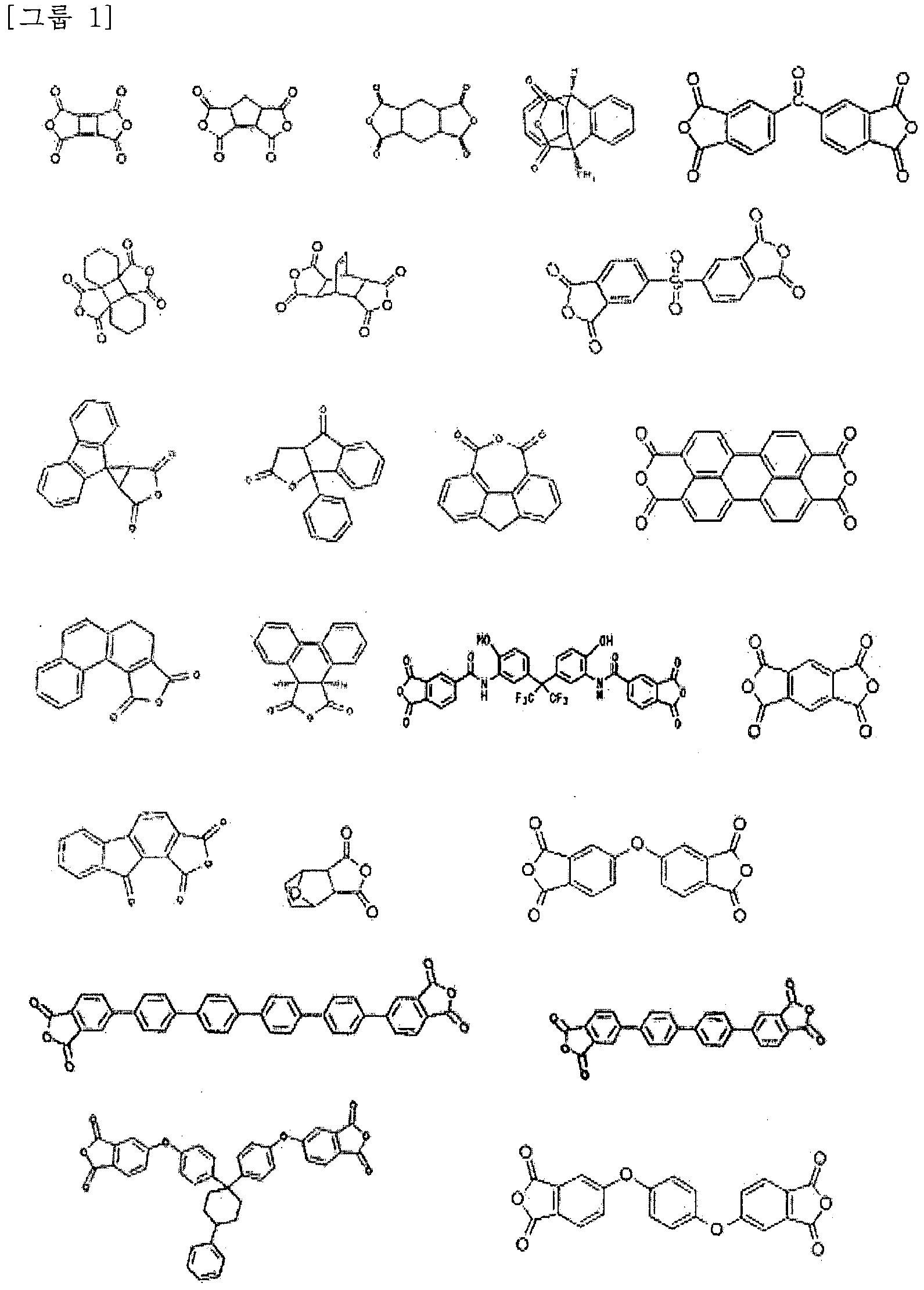
【청구항 3]
게 1항에서,
상기 A 및 A' 는 각각 독립적으로 치환 또는 비치환된 벤젠 기, 치환 또는 비 치환된 나프탈렌 기 , 치환 또는 비치환된 바이페닐 기, 치환 또는 비치환된 파이렌 기, 치환 또는 비치환된 퍼릴렌 기, 치환 또는 비치환된 벤조퍼릴렌 기, 치환 또는
비치환된 코로넨 기 또는 이들의 조합인 하드마스크 조성물용 모노머 .
【청구항 4】
제 1항에서 ,
상기 A' 는 적 어도 하나의 수소가 히드톡시기로 치환된 하드마스크 조성물용 모노머 .
【청구항 5】
제 1항에서,
상기 모노머는 하기 화학식 1-1, 1-2 또는 1-3으로 표현되는 하드마스크 조성 물용 모노머 .
[화학식 1-1]

[화학식 1-3]

상기 화학식 1-1, 1-2 및 1-3에서,
L' a, L' b, L' c, L' d, L' e 및 L' f는 각각 독립적으로 단일 결합 또는 치환 또는 비치환된 C1 내지 C6 알킬렌기이고
ma, mb, me 및 mf는 각각 독립적으로 0 내지 9인 정수이고,
mc 및 md는 각각 독립적으로 0 내지 11인 정수이다.
(단, ma, mb, mc, rad, me 및 mi는 치환된 히드록시 기의 수를 나타낸다ᅳ)
【청구항 6】
제 5항에서,
상기 모노머는 하기 화학식 1-la, 1-lb, l-2a, l-2b 또는 1— 3a로 표현되는 하 드마스크 조성물용 모노머:
[화학식 1-la]

[화학식 1-lb]


【청구항 7]
제 1항에서,
상기 모노머는 300 내지 3 ,000의 분자량을 가지는 하드마스크 조성물용 모노 .
【청구항 8]
거 U항 내지 제 7항 중 어느 한 항에 따른 모노머, 그리고
용매
를 포함하는 하드마스크 조성물.
【청구항 9】
제 8항에서,
상기 모노머는 상기 하드마스크 조성물 총함량에 대하여 1중량 % 내지 30 중량 %로 포함되어 '있는 하드마스크 조성물 .
【청구항 10】
기판 위 에 재료 층을 제공하는 단계,
상기 재료 층 위 에 제 8항에 따른 하드마스크 조성물을 적용하는 단계, 상기 하드마스크 조성물을 열처 리하여 하드마스크 층을 형성하는 단계, 상기 하드마스크 층 위에 실리콘 함유 박막층올 형성하는 단계,
상기 실리콘 함유 박막층 위에 포토레지스트 층을 형성하는 단계 ,
상가 포토레지스트 층을 노광 및 현상하여 포토레지스트 패턴을 형성하는 단 계,
상기 포토레지스트 패턴을 이용하여 상기 실리콘 함유 박막층 및 상기 하드마 스크 층을 선택적으로 제거하고 상기 재료 층의 일부를 노출하는 단계, 그리고 상기 재료 층의 노출된 부분을 식각하는 단계
를 포함하는 패턴 형성 방법 .
【청구항 111
제 10항에서,
상기 하드마스크 조성물을 적용하는 단계는 스핀-은 코팅 방법으로 수행하는 패턴 형성 방법 .
【청구항 12】
제 10항에서,
상기 하드마스크 층을 형성하는 단계는 100°C 내지 500°C에서 열처 리하는 패턴 형 성 방법 .
Priority Applications (2)
| Application Number | Priority Date | Filing Date | Title |
|---|---|---|---|
| US14/441,338 US9671688B2 (en) | 2012-12-28 | 2013-10-02 | Monomer for hardmask composition, hardmask composition including said monomer, and method for forming pattern using said hardmask composition |
| CN201380059123.6A CN104823106B (zh) | 2012-12-28 | 2013-10-02 | 硬掩膜组合物、用于其的单体及使用其形成图案的方法 |
Applications Claiming Priority (2)
| Application Number | Priority Date | Filing Date | Title |
|---|---|---|---|
| KR10-2012-0157570 | 2012-12-28 | ||
| KR1020120157570A KR101556276B1 (ko) | 2012-12-28 | 2012-12-28 | 하드마스크 조성물용 모노머, 상기 모노머를 포함하는 하드마스크 조성물 및 상기 하드마스크 조성물을 사용하는 패턴형성방법 |
Publications (1)
| Publication Number | Publication Date |
|---|---|
| WO2014104544A1 true WO2014104544A1 (ko) | 2014-07-03 |
Family
ID=51021559
Family Applications (1)
| Application Number | Title | Priority Date | Filing Date |
|---|---|---|---|
| PCT/KR2013/008836 Ceased WO2014104544A1 (ko) | 2012-12-28 | 2013-10-02 | 하드마스크 조성물용 모노머, 상기 모노머를 포함하는 하드마스크 조성물 및 상기 하드마스크 조성물을 사용하는 패턴형성방법 |
Country Status (5)
| Country | Link |
|---|---|
| US (1) | US9671688B2 (ko) |
| KR (1) | KR101556276B1 (ko) |
| CN (1) | CN104823106B (ko) |
| TW (1) | TWI535697B (ko) |
| WO (1) | WO2014104544A1 (ko) |
Families Citing this family (6)
| Publication number | Priority date | Publication date | Assignee | Title |
|---|---|---|---|---|
| US9556094B2 (en) * | 2012-12-26 | 2017-01-31 | Cheil Industries, Inc. | Monomer, hardmask composition including monomer, and method for forming pattern by using hardmask composition |
| KR101788093B1 (ko) * | 2014-03-19 | 2017-10-19 | 제일모직 주식회사 | 모노머, 상기 모노머를 포함하는 하드마스크 조성물 및 상기 하드마스크 조성물을 사용하는 패턴형성방법 |
| KR101806329B1 (ko) * | 2014-11-24 | 2017-12-07 | 삼성에스디아이 주식회사 | 모노머, 중합체, 유기막 조성물, 유기막, 및 패턴형성방법 |
| US9862668B2 (en) | 2014-11-24 | 2018-01-09 | Samsung Sdi Co., Ltd. | Monomer, polymer, organic layer composition, organic layer, and method of forming patterns |
| KR101941632B1 (ko) * | 2016-11-22 | 2019-01-24 | 동우 화인켐 주식회사 | 하드마스크용 조성물 |
| CN109912618B (zh) * | 2019-03-20 | 2020-12-25 | 浙江福斯特新材料研究院有限公司 | 一种多官能度有机酸酐及低介电常数超支化聚酰亚胺薄膜 |
Citations (5)
| Publication number | Priority date | Publication date | Assignee | Title |
|---|---|---|---|---|
| JP2006053404A (ja) * | 2004-08-13 | 2006-02-23 | Jsr Corp | 感放射線性組成物およびハードマスク形成材料 |
| US20070264828A1 (en) * | 2006-05-09 | 2007-11-15 | Hynix Semiconductor Inc. | Method for forming fine pattern of semiconductor device |
| KR20120068378A (ko) * | 2010-12-17 | 2012-06-27 | 제일모직주식회사 | 하드마스크 조성물, 이를 사용한 패턴 형성 방법 및 상기 패턴을 포함하는 반도체 집적회로 디바이스 |
| KR20120073817A (ko) * | 2010-12-27 | 2012-07-05 | 제일모직주식회사 | 하드마스크 조성물, 이를 사용한 패턴 형성 방법 및 상기 패턴을 포함하는 반도체 집적회로 디바이스 |
| KR20120077466A (ko) * | 2010-12-30 | 2012-07-10 | 제일모직주식회사 | 하드마스크 조성물, 이를 사용한 패턴 형성 방법 및 상기 패턴을 포함하는 반도체 집적회로 디바이스 |
Family Cites Families (17)
| Publication number | Priority date | Publication date | Assignee | Title |
|---|---|---|---|---|
| JP2654986B2 (ja) * | 1989-03-22 | 1997-09-17 | 富士ハントエレクトロニクステクノロジー株式会社 | フォトレジスト組成物 |
| JP3030473B2 (ja) * | 1990-05-11 | 2000-04-10 | 三井化学株式会社 | 新規なフルオラン化合物の製造方法 |
| JP3012904B1 (ja) * | 1998-12-10 | 2000-02-28 | 三洋化成工業株式会社 | サリチル酸誘導体の製造法 |
| JP2005505595A (ja) * | 2001-10-12 | 2005-02-24 | シェーリング コーポレイション | Cxc−ケモカインレセプターアンタゴニストとしての3,4−二置換マレイミド化合物 |
| ES2298832T3 (es) * | 2003-10-24 | 2008-05-16 | Glaxo Group Limited | Compuestos heterociclicos. |
| KR100665758B1 (ko) * | 2005-09-15 | 2007-01-09 | 제일모직주식회사 | 반사방지성을 갖는 하드마스크 조성물 |
| US7960544B2 (en) * | 2005-12-16 | 2011-06-14 | Ironwood Pharmaceuticals, Inc. | Useful indole compounds |
| KR20070095736A (ko) * | 2006-03-22 | 2007-10-01 | 제일모직주식회사 | 유기실란계 중합체를 포함하는 레지스트 하층막용 하드마스크 조성물 및 이를 이용한 반도체 집적회로 디바이스의 제조방법 |
| KR100835486B1 (ko) * | 2006-05-09 | 2008-06-04 | 주식회사 하이닉스반도체 | 반도체 소자의 미세패턴 형성방법 |
| US7416834B2 (en) | 2006-09-27 | 2008-08-26 | Az Electronic Materials Usa Corp. | Antireflective coating compositions |
| KR100888611B1 (ko) | 2007-06-05 | 2009-03-12 | 제일모직주식회사 | 반사방지 하드마스크 조성물 및 이를 이용한 기판상재료의 패턴화 방법 |
| JPWO2009038126A1 (ja) * | 2007-09-20 | 2011-01-06 | 日産化学工業株式会社 | 分岐型ポリヒドロキシスチレンを含むレジスト下層膜形成組成物 |
| KR101156489B1 (ko) | 2008-12-02 | 2012-06-18 | 제일모직주식회사 | 반사방지 하드마스크 조성물 |
| KR101212676B1 (ko) | 2008-12-31 | 2012-12-14 | 제일모직주식회사 | 고분자, 고분자 조성물, 이를 포함하는 레지스트 하층막 조성물 및 이를 이용하는 재료의 패턴화 방법 |
| DE102009022897A1 (de) * | 2009-05-27 | 2010-12-02 | Bayer Schering Pharma Aktiengesellschaft | Substituierte Piperidine |
| KR101311942B1 (ko) | 2009-12-31 | 2013-09-26 | 제일모직주식회사 | 레지스트 하층막용 방향족 고리 함유 화합물 및 이를 포함하는 레지스트 하층막용 조성물 |
| KR101344788B1 (ko) | 2010-12-17 | 2013-12-26 | 제일모직주식회사 | 하드마스크 조성물, 이를 사용한 패턴 형성 방법 및 상기 패턴을 포함하는 반도체 집적회로 디바이스 |
-
2012
- 2012-12-28 KR KR1020120157570A patent/KR101556276B1/ko active Active
-
2013
- 2013-10-02 CN CN201380059123.6A patent/CN104823106B/zh active Active
- 2013-10-02 US US14/441,338 patent/US9671688B2/en active Active
- 2013-10-02 WO PCT/KR2013/008836 patent/WO2014104544A1/ko not_active Ceased
- 2013-12-11 TW TW102145484A patent/TWI535697B/zh active
Patent Citations (5)
| Publication number | Priority date | Publication date | Assignee | Title |
|---|---|---|---|---|
| JP2006053404A (ja) * | 2004-08-13 | 2006-02-23 | Jsr Corp | 感放射線性組成物およびハードマスク形成材料 |
| US20070264828A1 (en) * | 2006-05-09 | 2007-11-15 | Hynix Semiconductor Inc. | Method for forming fine pattern of semiconductor device |
| KR20120068378A (ko) * | 2010-12-17 | 2012-06-27 | 제일모직주식회사 | 하드마스크 조성물, 이를 사용한 패턴 형성 방법 및 상기 패턴을 포함하는 반도체 집적회로 디바이스 |
| KR20120073817A (ko) * | 2010-12-27 | 2012-07-05 | 제일모직주식회사 | 하드마스크 조성물, 이를 사용한 패턴 형성 방법 및 상기 패턴을 포함하는 반도체 집적회로 디바이스 |
| KR20120077466A (ko) * | 2010-12-30 | 2012-07-10 | 제일모직주식회사 | 하드마스크 조성물, 이를 사용한 패턴 형성 방법 및 상기 패턴을 포함하는 반도체 집적회로 디바이스 |
Also Published As
| Publication number | Publication date |
|---|---|
| KR20140086730A (ko) | 2014-07-08 |
| KR101556276B1 (ko) | 2015-09-30 |
| TWI535697B (zh) | 2016-06-01 |
| US9671688B2 (en) | 2017-06-06 |
| CN104823106B (zh) | 2020-12-22 |
| CN104823106A (zh) | 2015-08-05 |
| US20150301446A1 (en) | 2015-10-22 |
| TW201425292A (zh) | 2014-07-01 |
Similar Documents
| Publication | Publication Date | Title |
|---|---|---|
| KR101754901B1 (ko) | 하드마스크 조성물 및 상기 하드마스크 조성물을 사용하는 패턴형성방법 | |
| CN108291013B (zh) | 聚合物、有机层组成物及图案形成方法 | |
| CN104749880B (zh) | 硬掩膜组合物和使用硬掩膜组合物形成图案的方法 | |
| KR101566533B1 (ko) | 하드마스크 조성물 및 이를 사용한 패턴형성방법 | |
| US9158201B2 (en) | Monomer for hardmask composition and hardmask composition including the monomer and method of forming patterns using the hardmask composition | |
| KR101599961B1 (ko) | 모노머, 상기 모노머를 포함하는 하드마스크 조성물 및 상기 하드마스크 조성물을 사용하는 패턴형성방법 | |
| CN105280481B (zh) | 硬掩膜组成物和使用所述硬掩膜组成物形成图案的方法 | |
| KR101666483B1 (ko) | 레지스트 하층막용 조성물, 이를 사용한 패턴 형성 방법 및 상기 패턴을 포함하는 반도체 집적회로 디바이스 | |
| KR20150079199A (ko) | 하드마스크 조성물, 이를 사용한 패턴 형성 방법 및 상기 패턴을 포함하는 반도체 집적회로 디바이스 | |
| WO2014104544A1 (ko) | 하드마스크 조성물용 모노머, 상기 모노머를 포함하는 하드마스크 조성물 및 상기 하드마스크 조성물을 사용하는 패턴형성방법 | |
| WO2018079936A1 (ko) | 중합체, 유기막 조성물 및 패턴형성방법 | |
| KR20130078432A (ko) | 하드마스크 조성물용 모노머, 상기 모노머를 포함하는 하드마스크 조성물 및 상기 하드마스크 조성물을 사용하는 패턴형성방법 | |
| WO2017126780A1 (ko) | 유기막 조성물, 및 패턴형성방법 | |
| WO2018021619A1 (ko) | 유기막 조성물 및 패턴형성방법 | |
| KR20130078745A (ko) | 하드마스크 조성물용 모노머, 상기 모노머를 포함하는 하드마스크 조성물 및 상기 하드마스크 조성물을 사용하는 패턴형성방법 | |
| TWI553030B (zh) | 硬遮罩組成物用單體、包含該單體之硬遮罩組成物及使用該硬遮罩組成物形成圖案之方法 | |
| KR101590810B1 (ko) | 모노머, 상기 모노머를 포함하는 하드마스크 조성물 및 상기 하드마스크 조성물을 사용하는 패턴형성방법 | |
| KR20160008928A (ko) | 모노머, 상기 모노머를 포함하는 하드마스크 조성물 및 상기 하드마스크 조성물을 사용하는 패턴형성방법 | |
| KR20140083844A (ko) | 하드마스크 조성물용 모노머, 상기 모노머를 포함하는 하드마스크 조성물 및 상기 하드마스크 조성물을 사용하는 패턴형성방법 | |
| WO2019088396A1 (ko) | 중합체, 유기막 조성물 및 패턴 형성 방법 | |
| JP2025024663A (ja) | ハードマスク組成物、ハードマスク層およびパターン形成方法 | |
| KR101937319B1 (ko) | 하드마스크 조성물용 모노머, 상기 모노머를 포함하는 하드마스크 조성물 및 상기 하드마스크 조성물을 사용하는 패턴형성방법 | |
| CN120370622A (zh) | 硬掩模组合物、硬掩模层和形成图案的方法 | |
| KR20150002931A (ko) | 하드마스크 조성물용 모노머, 상기 모노머를 포함하는 하드마스크 조성물 및 상기 하드마스크 조성물을 사용하는 패턴형성방법 | |
| WO2018088658A1 (ko) | 중합체, 유기막 조성물 및 패턴형성방법 |
Legal Events
| Date | Code | Title | Description |
|---|---|---|---|
| 121 | Ep: the epo has been informed by wipo that ep was designated in this application |
Ref document number: 13869572 Country of ref document: EP Kind code of ref document: A1 |
|
| WWE | Wipo information: entry into national phase |
Ref document number: 14441338 Country of ref document: US |
|
| NENP | Non-entry into the national phase |
Ref country code: DE |
|
| 122 | Ep: pct application non-entry in european phase |
Ref document number: 13869572 Country of ref document: EP Kind code of ref document: A1 |