WO2014097975A1 - ブラシ型接点材料及びその製造方法 - Google Patents
ブラシ型接点材料及びその製造方法 Download PDFInfo
- Publication number
- WO2014097975A1 WO2014097975A1 PCT/JP2013/083422 JP2013083422W WO2014097975A1 WO 2014097975 A1 WO2014097975 A1 WO 2014097975A1 JP 2013083422 W JP2013083422 W JP 2013083422W WO 2014097975 A1 WO2014097975 A1 WO 2014097975A1
- Authority
- WO
- WIPO (PCT)
- Prior art keywords
- brush
- tip
- nail
- type contact
- contact material
- Prior art date
- Legal status (The legal status is an assumption and is not a legal conclusion. Google has not performed a legal analysis and makes no representation as to the accuracy of the status listed.)
- Ceased
Links
Images




Classifications
-
- H—ELECTRICITY
- H01—ELECTRIC ELEMENTS
- H01R—ELECTRICALLY-CONDUCTIVE CONNECTIONS; STRUCTURAL ASSOCIATIONS OF A PLURALITY OF MUTUALLY-INSULATED ELECTRICAL CONNECTING ELEMENTS; COUPLING DEVICES; CURRENT COLLECTORS
- H01R39/00—Rotary current collectors, distributors or interrupters
-
- H—ELECTRICITY
- H01—ELECTRIC ELEMENTS
- H01C—RESISTORS
- H01C1/00—Details
- H01C1/12—Arrangements of current collectors
-
- H—ELECTRICITY
- H01—ELECTRIC ELEMENTS
- H01C—RESISTORS
- H01C10/00—Adjustable resistors
- H01C10/28—Adjustable resistors the contact rocking or rolling along resistive element or taps
-
- H—ELECTRICITY
- H01—ELECTRIC ELEMENTS
- H01R—ELECTRICALLY-CONDUCTIVE CONNECTIONS; STRUCTURAL ASSOCIATIONS OF A PLURALITY OF MUTUALLY-INSULATED ELECTRICAL CONNECTING ELEMENTS; COUPLING DEVICES; CURRENT COLLECTORS
- H01R43/00—Apparatus or processes specially adapted for manufacturing, assembling, maintaining, or repairing of line connectors or current collectors or for joining electric conductors
- H01R43/16—Apparatus or processes specially adapted for manufacturing, assembling, maintaining, or repairing of line connectors or current collectors or for joining electric conductors for manufacturing contact members, e.g. by punching and by bending
Definitions
- the present invention relates to a brush-type contact material used as a sliding contact for sensors such as a position sensor and a resistor such as a potentiometer.
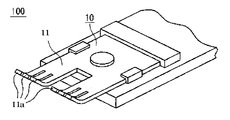
- a slider 100 is used for transmitting and receiving electrical signals, electric power, and the like to and from an assembly that moves in a straight line or the like (FIG. 1).
- the slider 100 is provided with a brush-type contact material 10 that slides the tip of the slider 100 on the sensor rotor or the like.
- the brush-type contact material 10 is a series of a plurality of claws 11 that are curved near the contact portion with the substrate.
- claw 11 is used in the state slidably contacted with the board
- a flat sliding contact piece (see FIG. 2) having no curvature is manufactured by stamping by pressing.
- the punching process often generates burrs on the outer periphery of the tip of the brush claw and becomes sharp. If burrs remain on the tip of the nail, the tip of the nail cannot slide smoothly, so the tip of the sliding contact piece after punching is generally processed into a curved surface.
- Barrel polishing was once used as a method for processing the tip of the sliding contact piece after punching into a curved surface.
- Barrel polishing is a method in which a polishing medium such as a grinding stone and a sliding contact piece that is pressed up are put into a container, and the entire outer peripheral surface of the sliding contact piece is polished by rotating the container.
- Barrel polishing is an efficient means because a large number of sliding contact pieces with small dimensions can be processed simultaneously.
- barrel polishing is not a method of intensively polishing a specific portion, but it is difficult to reliably process a curved surface only at the tip portion, and the polishing state is likely to vary.
- the applicant of the present application has proposed a manufacturing method using a laser beam and a contact material by this manufacturing method, in contrast to the method of manufacturing a brush-type contact material by barrel polishing.
- a laser beam is sequentially irradiated to the tip of the nail of the press-up sliding contact piece to melt and solidify the tip of the nail.
- only the tip of the nail can be processed into a curved surface, and a constant quality material without variation can be efficiently manufactured by making the irradiation condition of the laser beam appropriate.
- the brush-type contact material produced by this method has a smooth curved surface at the tip of the nail, and has a smooth curved surface shape such as a circular arc cross section. Has been.
- the brush-type contact material requires smooth sliding movement of the tip of the nail, and the well-balanced curved surface shape formed by the laser processing described above responds to this once. It is what However, there is a demand for a smoother sliding operation. Further, in the curved surface processing with the laser processing described above, the material structure of the melted / solidified portion after laser irradiation is changed and the hardness is lowered, it is easily consumed and deformed locally, and it is difficult to maintain the curved surface shape. Therefore, it is necessary to adjust the hardness by performing a heat treatment after laser irradiation, but this heat treatment leads to an increase in the number of steps in the contact material manufacturing process.
- the melted and solidified tip shape tends to approach a spherical shape, but it is impossible to control the shape at that time.
- the central portion of the bowl-shaped curved surface is raised and concentrated, and stable sliding cannot be obtained.
- the present invention discloses a brush-type contact material that can perform a smoother sliding operation and can be manufactured relatively easily, and a manufacturing method thereof.
- the present invention that solves the above-mentioned problems is a brush-type contact material having one or more curved metal claws whose tip part contacts an object to be contacted, wherein the tip part of the claw is a cross section in the thickness direction. It has an arc shape and is formed such that a curvature radius R1 from the contact point to the contacted object and the curvature radius R2 from the contact point to the back side satisfies R1 ⁇ R2, and further, the width direction of the nail Is a brush-type contact material formed by chamfering both ends.
- the brush-type contact material according to the present invention includes the case where the front and back sides have different curvature radii, as well as the shape of the claw tip having a circular arc shape and uniform curvature radius. Further, the both ends in the width direction of the nail are subjected to a forming process by chamfering.
- chamfering is also performed on both ends in the width direction of the nail because, when an unbalanced load occurs during contact use, local wear may occur at the mating contact if the corners of both ends of the nail are sharp It is. And it has the merit which reduces the local wear by the eccentric load at the time of use by chamfering both ends of a nail
- R1 / R2 is 3.0 or less.
- the nail curve is set so that the brush and the substrate come into contact with each other at an angle of 70 to 85 degrees (see FIG. 3).
- R1 / R2 1.0 to 3.0, the connecting position of R1 and R2 becomes an approximate position with the contact point, and stable sliding is exhibited.
- the present invention chamfers both ends, and this chamfered portion is chamfered in the range of both ends W / 10 to W / 4 of the brush width W. What was processed is preferable.
- the shape of this processed portion is preferably chamfer removal (R-connection) of 10 ° to 45 ° or R-chamfering of R0.15 to R0.5 (see FIG. 4). This is to prevent the occurrence of burrs and ensure stable contact.
- the same metal as the conventional contact material is applied.
- an Ag-based alloy for example, Ag: 39.5 wt%, Pd: 43.0 wt%, Cu: 17.0 wt%, Pt: 0.5 wt%, or Pt 10 wt%, Au: 10 wt%, Ag: 30 wt%) , Pd: 35 wt%, Cu: 14 wt%, Zn: 1 wt%, etc.
- an Ag-based alloy for example, Ag: 39.5 wt%, Pd: 43.0 wt%, Cu: 17.0 wt%, Pt: 0.5 wt%, or Pt 10 wt%, Au: 10 wt%, Ag: 30 wt%)
- the brush-type contact material In the production of the brush-type contact material according to the present invention, first, a strip material having a plurality of claws is punched from a metal plate. Thereafter, the shape of the tip of the claw of the band plate material is processed into the shape described above, but this processing method may be based on laser processing by the applicant of the present application. By using laser processing, it is possible to form a curved surface with an even cross-sectional arc shape while smoothing the tip of the nail. And it can chamfer by grind
- Processing of the nail tip by laser processing is performed by sequentially irradiating the nail tip with a laser beam in a state in which the band plate material after the punching process is held, thereby melting and solidifying the nail tip.
- the hardness is adjusted by heat treatment.
- the manufacturing method applying the above laser processing can obtain a uniform arc shape (R1 and R2 are approximately equal) by setting the conditions, but R1 and R2 cannot be formed separately, Can not adjust the relationship. Moreover, in order to ensure hardness, the heat processing after laser processing is essential, and the number of processes increases. Therefore, it is preferable to fix the band plate material after the punching process and to polish the claw tip portion sequentially with a grindstone.
- the tip shape of the nail can be freely shaped by adjusting the position and angle to which the grinding wheel is applied, and in particular, the tip part having a different R can be formed partially. Further, the surface roughness of the tip of the nail can be adjusted by appropriately selecting the particle size of the grindstone. Furthermore, since molding by mechanical polishing can be processed without generating a heat-affected zone or changing the metal structure, the polished material can be used as it is.
- ⁇ Nail tip processing by polishing involves bringing the grindstone into contact with the tip of the nail, but at this time, the band plate material is set so that the tip of the nail is semi-fixed. During this processing, the semi-fixed band plate material tends to escape from the grindstone, while the grindstone attempts to bite the band plate material. By utilizing this contradictory movement, the tip of the nail can be gradually and properly polished into an R shape.
- R on the front and back of the claw tip and chamfering of the end can be controlled by the holding angle of the band plate material when polishing, the supply speed, the grinding stone cutting amount, and the rotation speed. In this process, it is preferable to mask other than the polished portion at the tip of the claw of the strip after punching.
- the brush-type contact material according to the present invention is to appropriately shape the shape of the tip of the nail, and can be smoothly slid with respect to the counterpart substrate, while maintaining the hardness of the constituent metals.
- the brush-type contact material according to the present invention can be manufactured through a processing step of the nail tip by grinding stone grinding.
- a material having a composition of 39.5 wt% Ag, 43.0 wt% Pd, 17.0 wt% Cu, 0.5 wt% Pt was subjected to rolling or the like to prepare a thin plate material having a width of 23 mm and a thickness of 0.12 mm. Then, this thin plate material was pressed to obtain a strip plate material 1 in which a plurality of sliding contact pieces 10 'as shown in FIG.
- Each sliding contact piece 10 ′ is composed of a base 12 and two brushes 11 ′ extending from the base 12.
- the sliding contact pieces 10 ′ adjacent to each other through a cutting margin 13 in the base 12 portion. It is connected to.
- Each brush 11 ' has three claws (width dimension is 0.4 mm) of the same length arranged in a comb shape. Further, both the brushes 11 ′ are arranged such that the claw tips 11 a ′ are arranged in parallel, and the claw tips are arranged in a straight line.
- FIG. 5 is a photograph showing the state of the tip of the press-up nail.
- the surface of the claw tip 11a 'at this stage was in a rough state as it was punched out by pressing.
- tip part was left-right asymmetric, and the outline of the inward process front-end
- the tip of the nail was processed by polishing.
- the polishing process was performed by masking a portion other than the claw tip polishing portion 11a 'of the punched strip, holding the cutting margin 13 and supplying it under the grindstone, and in a semi-fixed state.
- the grindstone was contacted and passed through the tip polishing portion 11a 'while rotating and swinging from the vertical direction of the band plate material with a width capable of simultaneously polishing a plurality of nail tip polishing portions 11a'.
- the processing of the tip of the nail where R1 and R2 on the front and back sides are different controlled the holding angle and supply speed of the band plate material at the time of polishing, the grinding stone cutting amount, and the rotation speed.
- the polishing angle of the strips of Examples 1 to 3 shown below was 45 °.
- the band plate materials of Examples 4 to 6 were processed by changing the grinding wheel cutting amount and the number of revolutions of the grinding wheel while keeping the same polishing angle of 30 °.
- a brush-type contact material in which sliding contacts having curved claws are formed in a band shape by bending is obtained.
- the shape of the claw tip in each example is as follows.
- claw tip part are measured in the cross section of the center part of a nail
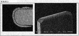
- FIG. 6 and 7 are photographs showing the tips of the claws 11a of the brush-type contact material of Example 1 and Example 3, respectively.
- the surface state of the tip of the nail of the obtained brush-type contact material was a smooth surface state.
- R on the front side and the back side have different shapes. Further, both end portions have inclinations that are chamfered.
- FIG. 8 is a photograph showing the tip of the claw 11a of Examples 4 to 6. The shape of the claw tip portion of these examples was a so-called wrinkle shape that was uniform throughout.
- FIG. 9 is a schematic diagram of a brush evaluation circuit, in which a brush-type contact material is horizontally mounted on a substrate having an arc-shaped resistor, and an output is 0V at an angle of 0 ° and an output of 5V at an angle of 90 °.
- the brush-type contact material was slid 2 million times on the resistor shown in FIG. 9, and then the electrical characteristics (linearity (linearity)) were measured. The linearity was measured by applying a constant voltage to the resistor shown in FIG. 9 and measuring the sensor output voltage (angle vs.
- the linearity is evaluated based on the change rate% as the displacement of the difference between the output potential from the brush and the reference output voltage (theoretical output).
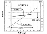
- FIG. 10 is an example of the linearity measurement result, and shows the linearity measurement result after endurance in Example 1.
- Angle-voltage data refers to the left main scale, and linearity refers to the right sub-scale.
- the linearity of this example has a width (linearity) of ⁇ 0.7% with respect to the theoretical value, and has excellent linearity even after the durability test.
- linearity within ⁇ 2.0% is required as an in-vehicle component standard for clearing automobile exhaust gas regulations. This standard is expected to become stricter in the future, and a linearity of ⁇ 1.5% may be required for further performance improvement.
- the contact material of Example 1 can cope with this strict standard.
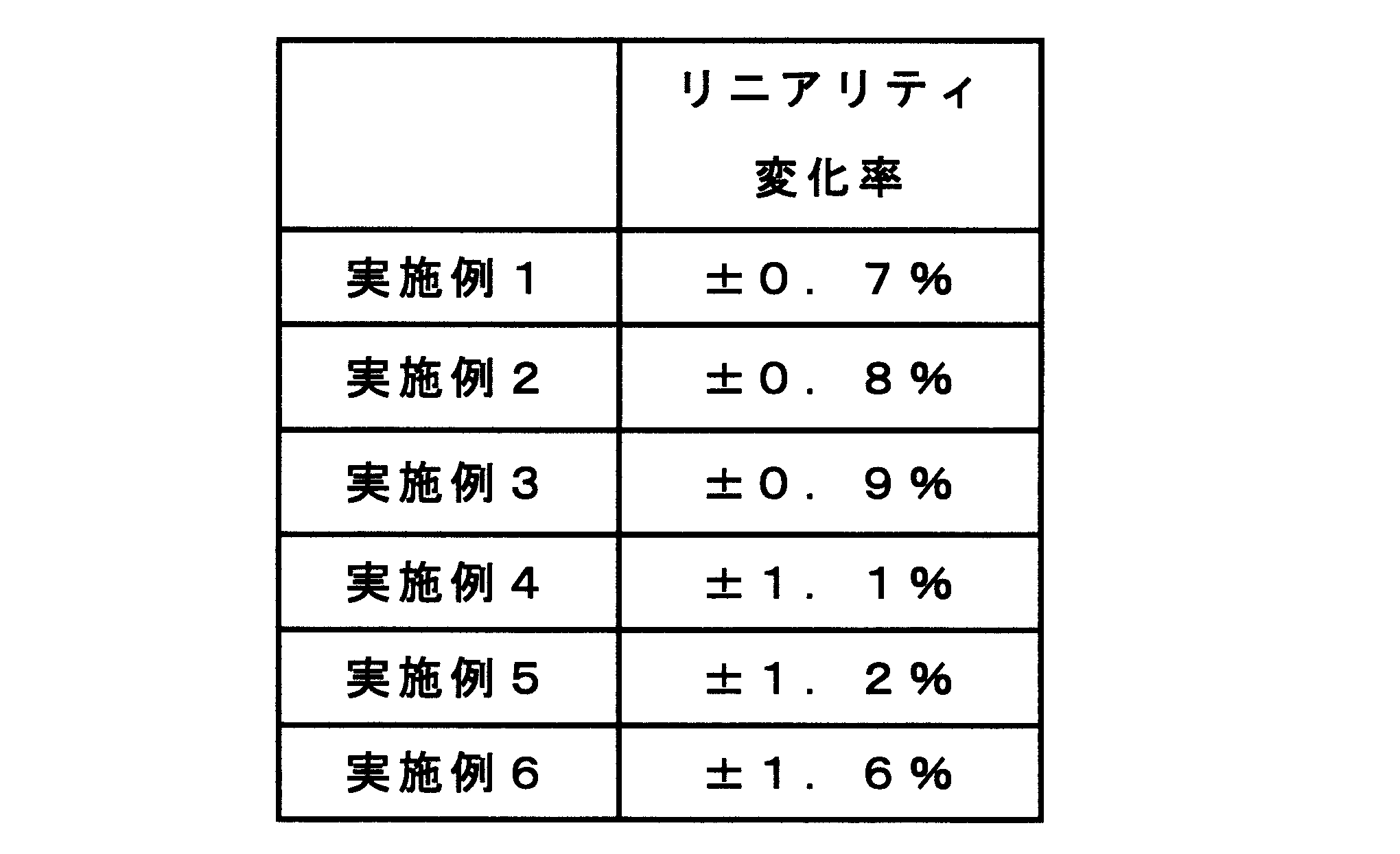
- Table 2 shows the linearity measurement results for each example.
- the brush-type contact materials of Examples 1 to 6 all have a linearity of ⁇ 2% or less, and have characteristics that can clear the current in-vehicle component standards. Further, it was confirmed that an extremely excellent characteristic result of ⁇ 1% or less can be obtained by making a difference between R1 and R2 as in Example 1.
- the brush-type contact material according to the present invention enables a smoother sliding operation than before as a result of detailed examination of the shape of the tip of the nail.
- the brush-type contact material can be manufactured relatively easily, and can be manufactured without changing the mechanical properties of the constituent material without requiring heat treatment after molding.
- the present invention is suitable as a contact material for a slider in sensors and resistors such as a position sensor.
Landscapes
- Engineering & Computer Science (AREA)
- Microelectronics & Electronic Packaging (AREA)
- Manufacturing & Machinery (AREA)
- Manufacturing Of Electrical Connectors (AREA)
- Adjustable Resistors (AREA)
- Apparatuses And Processes For Manufacturing Resistors (AREA)
- Details Of Resistors (AREA)
Abstract
Description

Claims (4)
- その先端部が被接触対象物に接触する湾曲した金属製の爪を1つ以上有するブラシ型接点材料において、
前記爪の前記先端部は、厚さ方向断面で円弧形状を有し、被接触対象物との接触点から表側の曲率半径R1と、接触点から裏側の曲率半径R2とがR1≧R2となるように成形されており、更に、爪の幅方向の両端部が面取り加工されてなるブラシ型接点材料。 - R1>R2であり、R1/R2が3.0以下である請求項1記載のブラシ型接点材料。
- 爪の幅方向の両端部の面取り加工は、ブラシ幅Wの両端部W/10~W/4の範囲でなされる、チャンファー取り加工又はR面取り加工である請求項1又は請求項2記載のブラシ型接点材料。
- 請求項1~請求項3のいずれかに記載のブラシ型接点材料の製造方法であって、
薄板から、金属製の爪が複数連なってなる帯板材を打抜き加工する工程と、
前記帯板材を半固定の状態で保持し、前記爪の先端部に砥石を当接して研磨することによって成形加工する工程と、を含むブラシ型接点材料の製造方法。
Priority Applications (3)
| Application Number | Priority Date | Filing Date | Title |
|---|---|---|---|
| KR1020157016244A KR101814885B1 (ko) | 2012-12-21 | 2013-12-13 | 브러시형 접점 재료 및 그 제조 방법 |
| CN201380067260.4A CN104937679B (zh) | 2012-12-21 | 2013-12-13 | 电刷型触点材料及其制造方法 |
| US14/652,195 US9601888B2 (en) | 2012-12-21 | 2013-12-13 | Brush type contact material and manufacturing method for the same |
Applications Claiming Priority (2)
| Application Number | Priority Date | Filing Date | Title |
|---|---|---|---|
| JP2012279443A JP5992821B2 (ja) | 2012-12-21 | 2012-12-21 | ブラシ型接点材料及びその製造方法 |
| JP2012-279443 | 2012-12-21 |
Publications (1)
| Publication Number | Publication Date |
|---|---|
| WO2014097975A1 true WO2014097975A1 (ja) | 2014-06-26 |
Family
ID=50978309
Family Applications (1)
| Application Number | Title | Priority Date | Filing Date |
|---|---|---|---|
| PCT/JP2013/083422 Ceased WO2014097975A1 (ja) | 2012-12-21 | 2013-12-13 | ブラシ型接点材料及びその製造方法 |
Country Status (5)
| Country | Link |
|---|---|
| US (1) | US9601888B2 (ja) |
| JP (1) | JP5992821B2 (ja) |
| KR (1) | KR101814885B1 (ja) |
| CN (1) | CN104937679B (ja) |
| WO (1) | WO2014097975A1 (ja) |
Families Citing this family (4)
| Publication number | Priority date | Publication date | Assignee | Title |
|---|---|---|---|---|
| DE102018213999A1 (de) * | 2018-08-20 | 2020-02-20 | Spinner Gmbh | Gleitkontaktkörper sowie elektrischer Drehübertrager |
| US12145237B2 (en) * | 2018-12-21 | 2024-11-19 | Sdns, Inc. | Speed-controlled auto brushing of rules |
| CN109692909B (zh) * | 2019-01-14 | 2023-12-15 | 上海徕木电子股份有限公司 | 一种连接器用鱼叉形端子的制备工艺 |
| CN112992452B (zh) * | 2021-05-18 | 2021-08-03 | 成都宏明电子股份有限公司 | 基于点焊的电位器簧片组件制造方法 |
Citations (4)
| Publication number | Priority date | Publication date | Assignee | Title |
|---|---|---|---|---|
| JPH05226103A (ja) * | 1992-02-17 | 1993-09-03 | Tanaka Kikinzoku Kogyo Kk | 摺動接点 |
| JPH06289051A (ja) * | 1993-04-02 | 1994-10-18 | Kobe Steel Ltd | 金属線材及びその製造方法 |
| JP2001351807A (ja) * | 2000-06-09 | 2001-12-21 | Tokyo Cosmos Electric Co Ltd | 可変抵抗器用摺動子 |
| JP2003347110A (ja) * | 2002-05-23 | 2003-12-05 | Tanaka Kikinzoku Kogyo Kk | 摺動接点およびその製造方法 |
Family Cites Families (10)
| Publication number | Priority date | Publication date | Assignee | Title |
|---|---|---|---|---|
| DE2125609A1 (de) * | 1968-05-13 | 1972-12-14 | Illinois Tool Works | Federkontakt sowie Verfahren zur Herstellung desselben.- |
| CA989318A (en) * | 1972-12-28 | 1976-05-18 | Fujio Oda | Record stylus |
| JPS5826764B2 (ja) * | 1978-10-31 | 1983-06-04 | 新光電気工業株式会社 | 多接点接触ばねの製造方法 |
| US4928083A (en) * | 1989-04-10 | 1990-05-22 | Colt Industries Inc. | Wiper for variable electrical resistor |
| US5485049A (en) * | 1994-05-25 | 1996-01-16 | United Technologies Motor Systems, Inc. | Multi-speed motor |
| GB0303752D0 (en) * | 2003-02-18 | 2003-03-26 | Morgan Crucible Co | Composite electrical brush construction |
| JP2005039037A (ja) * | 2003-07-14 | 2005-02-10 | Tanaka Kikinzoku Kogyo Kk | 摺動子 |
| JP5048665B2 (ja) * | 2006-06-02 | 2012-10-17 | 北陸電気工業株式会社 | 可変抵抗器 |
| US9536815B2 (en) * | 2009-05-28 | 2017-01-03 | Hsio Technologies, Llc | Semiconductor socket with direct selective metalization |
| US20120058692A1 (en) * | 2010-09-02 | 2012-03-08 | Cheng Uei Precision Industry Co., Ltd | Contact of electrical connector and plating method thereof |
-
2012
- 2012-12-21 JP JP2012279443A patent/JP5992821B2/ja active Active
-
2013
- 2013-12-13 US US14/652,195 patent/US9601888B2/en active Active
- 2013-12-13 CN CN201380067260.4A patent/CN104937679B/zh active Active
- 2013-12-13 KR KR1020157016244A patent/KR101814885B1/ko active Active
- 2013-12-13 WO PCT/JP2013/083422 patent/WO2014097975A1/ja not_active Ceased
Patent Citations (4)
| Publication number | Priority date | Publication date | Assignee | Title |
|---|---|---|---|---|
| JPH05226103A (ja) * | 1992-02-17 | 1993-09-03 | Tanaka Kikinzoku Kogyo Kk | 摺動接点 |
| JPH06289051A (ja) * | 1993-04-02 | 1994-10-18 | Kobe Steel Ltd | 金属線材及びその製造方法 |
| JP2001351807A (ja) * | 2000-06-09 | 2001-12-21 | Tokyo Cosmos Electric Co Ltd | 可変抵抗器用摺動子 |
| JP2003347110A (ja) * | 2002-05-23 | 2003-12-05 | Tanaka Kikinzoku Kogyo Kk | 摺動接点およびその製造方法 |
Also Published As
| Publication number | Publication date |
|---|---|
| US9601888B2 (en) | 2017-03-21 |
| CN104937679B (zh) | 2017-11-24 |
| JP2014123657A (ja) | 2014-07-03 |
| US20150318651A1 (en) | 2015-11-05 |
| KR101814885B1 (ko) | 2018-01-04 |
| KR20150086353A (ko) | 2015-07-27 |
| CN104937679A (zh) | 2015-09-23 |
| JP5992821B2 (ja) | 2016-09-14 |
Similar Documents
| Publication | Publication Date | Title |
|---|---|---|
| JP5992821B2 (ja) | ブラシ型接点材料及びその製造方法 | |
| JP4105631B2 (ja) | チップ用ホルダー及びその製造方法並びにそのチップ用ホルダーを備えるスクライブ装置及び手動カッター | |
| US20170274491A1 (en) | Optical element processing tool and optical element manufacturing method | |
| CN116323041B (zh) | 烧结齿轮的制造方法 | |
| CN1318156C (zh) | 金刚石拉丝模具的制造方法 | |
| US8708781B2 (en) | Systems and methods for grinding refractory metals and refractory metal alloys | |
| CN106232251B (zh) | 金属线材拉丝加工用模具及其制造方法 | |
| KR100704689B1 (ko) | 슬라이딩 접점 및 그 제조방법 | |
| JP4852892B2 (ja) | ツルーイング工具および研削砥石のツルーイング方法 | |
| CN118905650A (zh) | 一种金属料带削边设备及其生产工艺 | |
| JP6878999B2 (ja) | 打抜き加工用金型及びそれを用いた打抜き加工方法 | |
| JP2003211333A (ja) | 工作機械の摺動案内構造 | |
| JP4708123B2 (ja) | ブラシ付き回転電機及びその製造方法 | |
| CN110026913B (zh) | 金刚石磨具刀头及其制备方法 | |
| JP2005152256A (ja) | 往復刃の製造方法及びこれを用いて製造した往復刃 | |
| JP2001138196A (ja) | 研磨工具の製造方法、研磨加工方法、研磨工具及び光学素子またはその金型 | |
| KR101477118B1 (ko) | 워크롤의 표면경도 향상방법 | |
| JP2002028843A (ja) | 固定砥粒の形成方法および固定砥粒の形成工具の製作方法 | |
| JPH08309667A (ja) | レジンボンド超砥粒ホイール | |
| RU2193962C1 (ru) | Композиционный шлифовальный круг | |
| JPWO2005077612A1 (ja) | 梳鋏に用いられる櫛刃の製造方法と梳鋏 | |
| JP2002264017A (ja) | 微細形状の加工装置及び加工方法 | |
| JP2004249384A (ja) | 両頭平面研削用ホイール | |
| JP2003048033A (ja) | Vgsタイプターボチャージャにおける排気ガイドアッセンブリに適用される可変翼の軸部の転造方法 | |
| JP2006297562A (ja) | 研削加工方法、成形用金型及び光学素子 |
Legal Events
| Date | Code | Title | Description |
|---|---|---|---|
| 121 | Ep: the epo has been informed by wipo that ep was designated in this application |
Ref document number: 13864314 Country of ref document: EP Kind code of ref document: A1 |
|
| WWE | Wipo information: entry into national phase |
Ref document number: 14652195 Country of ref document: US |
|
| ENP | Entry into the national phase |
Ref document number: 20157016244 Country of ref document: KR Kind code of ref document: A |
|
| NENP | Non-entry into the national phase |
Ref country code: DE |
|
| 122 | Ep: pct application non-entry in european phase |
Ref document number: 13864314 Country of ref document: EP Kind code of ref document: A1 |