WO2014088252A1 - 구리산화물 나노 구조체의 제조방법 및 리튬이온 이차전지용 음극의 제조방법 - Google Patents
구리산화물 나노 구조체의 제조방법 및 리튬이온 이차전지용 음극의 제조방법 Download PDFInfo
- Publication number
- WO2014088252A1 WO2014088252A1 PCT/KR2013/010768 KR2013010768W WO2014088252A1 WO 2014088252 A1 WO2014088252 A1 WO 2014088252A1 KR 2013010768 W KR2013010768 W KR 2013010768W WO 2014088252 A1 WO2014088252 A1 WO 2014088252A1
- Authority
- WO
- WIPO (PCT)
- Prior art keywords
- copper oxide
- negative electrode
- secondary battery
- lithium ion
- ion secondary
- Prior art date
- Legal status (The legal status is an assumption and is not a legal conclusion. Google has not performed a legal analysis and makes no representation as to the accuracy of the status listed.)
- Ceased
Links
Images





Classifications
-
- H—ELECTRICITY
- H01—ELECTRIC ELEMENTS
- H01M—PROCESSES OR MEANS, e.g. BATTERIES, FOR THE DIRECT CONVERSION OF CHEMICAL ENERGY INTO ELECTRICAL ENERGY
- H01M4/00—Electrodes
- H01M4/02—Electrodes composed of, or comprising, active material
- H01M4/13—Electrodes for accumulators with non-aqueous electrolyte, e.g. for lithium-accumulators; Processes of manufacture thereof
- H01M4/139—Processes of manufacture
- H01M4/1391—Processes of manufacture of electrodes based on mixed oxides or hydroxides, or on mixtures of oxides or hydroxides, e.g. LiCoOx
-
- C—CHEMISTRY; METALLURGY
- C25—ELECTROLYTIC OR ELECTROPHORETIC PROCESSES; APPARATUS THEREFOR
- C25D—PROCESSES FOR THE ELECTROLYTIC OR ELECTROPHORETIC PRODUCTION OF COATINGS; ELECTROFORMING; APPARATUS THEREFOR
- C25D3/00—Electroplating: Baths therefor
- C25D3/02—Electroplating: Baths therefor from solutions
- C25D3/38—Electroplating: Baths therefor from solutions of copper
-
- C—CHEMISTRY; METALLURGY
- C25—ELECTROLYTIC OR ELECTROPHORETIC PROCESSES; APPARATUS THEREFOR
- C25D—PROCESSES FOR THE ELECTROLYTIC OR ELECTROPHORETIC PRODUCTION OF COATINGS; ELECTROFORMING; APPARATUS THEREFOR
- C25D9/00—Electrolytic coating other than with metals
- C25D9/04—Electrolytic coating other than with metals with inorganic materials
- C25D9/08—Electrolytic coating other than with metals with inorganic materials by cathodic processes
-
- C—CHEMISTRY; METALLURGY
- C25—ELECTROLYTIC OR ELECTROPHORETIC PROCESSES; APPARATUS THEREFOR
- C25D—PROCESSES FOR THE ELECTROLYTIC OR ELECTROPHORETIC PRODUCTION OF COATINGS; ELECTROFORMING; APPARATUS THEREFOR
- C25D9/00—Electrolytic coating other than with metals
- C25D9/04—Electrolytic coating other than with metals with inorganic materials
- C25D9/08—Electrolytic coating other than with metals with inorganic materials by cathodic processes
- C25D9/10—Electrolytic coating other than with metals with inorganic materials by cathodic processes on iron or steel
-
- H—ELECTRICITY
- H01—ELECTRIC ELEMENTS
- H01M—PROCESSES OR MEANS, e.g. BATTERIES, FOR THE DIRECT CONVERSION OF CHEMICAL ENERGY INTO ELECTRICAL ENERGY
- H01M10/00—Secondary cells; Manufacture thereof
- H01M10/05—Accumulators with non-aqueous electrolyte
- H01M10/052—Li-accumulators
-
- H—ELECTRICITY
- H01—ELECTRIC ELEMENTS
- H01M—PROCESSES OR MEANS, e.g. BATTERIES, FOR THE DIRECT CONVERSION OF CHEMICAL ENERGY INTO ELECTRICAL ENERGY
- H01M4/00—Electrodes
- H01M4/02—Electrodes composed of, or comprising, active material
- H01M4/04—Processes of manufacture in general
- H01M4/0438—Processes of manufacture in general by electrochemical processing
- H01M4/045—Electrochemical coating; Electrochemical impregnation
- H01M4/0452—Electrochemical coating; Electrochemical impregnation from solutions
-
- H—ELECTRICITY
- H01—ELECTRIC ELEMENTS
- H01M—PROCESSES OR MEANS, e.g. BATTERIES, FOR THE DIRECT CONVERSION OF CHEMICAL ENERGY INTO ELECTRICAL ENERGY
- H01M4/00—Electrodes
- H01M4/02—Electrodes composed of, or comprising, active material
- H01M4/13—Electrodes for accumulators with non-aqueous electrolyte, e.g. for lithium-accumulators; Processes of manufacture thereof
- H01M4/131—Electrodes based on mixed oxides or hydroxides, or on mixtures of oxides or hydroxides, e.g. LiCoOx
-
- H—ELECTRICITY
- H01—ELECTRIC ELEMENTS
- H01M—PROCESSES OR MEANS, e.g. BATTERIES, FOR THE DIRECT CONVERSION OF CHEMICAL ENERGY INTO ELECTRICAL ENERGY
- H01M4/00—Electrodes
- H01M4/02—Electrodes composed of, or comprising, active material
- H01M4/36—Selection of substances as active materials, active masses, active liquids
- H01M4/48—Selection of substances as active materials, active masses, active liquids of inorganic oxides or hydroxides
-
- H—ELECTRICITY
- H01—ELECTRIC ELEMENTS
- H01M—PROCESSES OR MEANS, e.g. BATTERIES, FOR THE DIRECT CONVERSION OF CHEMICAL ENERGY INTO ELECTRICAL ENERGY
- H01M4/00—Electrodes
- H01M4/02—Electrodes composed of, or comprising, active material
- H01M4/36—Selection of substances as active materials, active masses, active liquids
- H01M4/48—Selection of substances as active materials, active masses, active liquids of inorganic oxides or hydroxides
- H01M4/485—Selection of substances as active materials, active masses, active liquids of inorganic oxides or hydroxides of mixed oxides or hydroxides for inserting or intercalating light metals, e.g. LiTi2O4 or LiTi2OxFy
-
- Y—GENERAL TAGGING OF NEW TECHNOLOGICAL DEVELOPMENTS; GENERAL TAGGING OF CROSS-SECTIONAL TECHNOLOGIES SPANNING OVER SEVERAL SECTIONS OF THE IPC; TECHNICAL SUBJECTS COVERED BY FORMER USPC CROSS-REFERENCE ART COLLECTIONS [XRACs] AND DIGESTS
- Y02—TECHNOLOGIES OR APPLICATIONS FOR MITIGATION OR ADAPTATION AGAINST CLIMATE CHANGE
- Y02E—REDUCTION OF GREENHOUSE GAS [GHG] EMISSIONS, RELATED TO ENERGY GENERATION, TRANSMISSION OR DISTRIBUTION
- Y02E60/00—Enabling technologies; Technologies with a potential or indirect contribution to GHG emissions mitigation
- Y02E60/10—Energy storage using batteries
Definitions
- the present invention relates to a method for manufacturing a nanostructure, and more particularly, to a method for manufacturing a copper oxide nanostructure and a method for manufacturing a negative electrode for a lithium ion secondary battery using the same.
- the active material of the negative electrode of a lithium secondary battery As the active material of the negative electrode of a lithium secondary battery, graphite and carbon, which are excellent in life and stability, are commercially used.
- a carbon-based negative electrode active material has a theoretical energy density of 372mAh / g has a disadvantage that has a relatively very low capacity compared to the negative electrode active material based on other metals and metal oxides.
- a lithium secondary battery using graphite or carbon as a negative electrode active material has a disadvantage in that the process is complicated by using a binder in the manufacturing process.
- negative electrode active materials using silicon and tin-based metals and metal oxides have a theoretical energy density of 700 mAh / g or more, and have twice as high energy density as carbon-based negative electrode active materials, but lithium ions during partial charging or discharging In the process of inserting and detaching into the negative electrode active material has a problem that causes the volume expansion of more than 300%. As such, the volume expansion of the negative electrode active material has a disadvantage that stress builds up in the material, causing mechanical cracking of the negative electrode active material and consequently shortening the life of the lithium secondary battery.
- the present invention has been made to solve various problems including the above problems, and an object thereof is to provide an economical manufacturing method of a copper oxide nanostructure and an economical manufacturing method of a negative electrode for a lithium secondary battery using the same.
- these problems are exemplary, and the scope of the present invention is not limited thereby.
- the step of immersing the negative electrode current collector in an electrolytic solution containing copper ions Forming a negative electrode active material by growing a copper oxide nanostructure on the negative electrode current collector immersed in the electrolytic solution by an electroplating method; It provides a method of manufacturing a negative electrode for a lithium ion secondary battery comprising a.
- the forming of the negative electrode active material may include directly growing the copper oxide nanostructure on the negative electrode current collector without a template.
- the copper oxide nanostructures may include copper oxide nanoparticles, copper oxide nanowires, copper oxide nanofibers, or copper oxide nanorods.
- the copper oxide nanostructure may extend upward from an upper surface of the negative electrode current collector.
- the copper oxide nanostructure may have a growth length of 0.1 ⁇ m to 500 ⁇ m.
- the copper oxide nanostructure includes any one or a mixture of two or more selected from the group consisting of Cu 2 O, CuO, Cu 2 O 3 , CuO 2 and Cu 3 O 4 . can do.
- the negative electrode current collector may include copper, stainless steel, or nickel.
- the electroplating method may be performed at room temperature.
- the electrolytic solution may include a copper sulfate solution, and the electroplating method may be performed in a potentiodynamic mode.
- the immersing may include immersing an Ag / AgCl reference electrode in the electrolyte solution; And immersing the Pt mesh counter electrode in the electrolyte solution.
- the present invention made as described above, it is possible to manufacture a copper oxide nanostructure on a substrate economically without a template. Furthermore, by using the copper oxide nanostructure as a negative electrode for a lithium ion secondary battery, it is possible to improve its capacity and lifetime and to simplify its manufacturing process without increasing the volume change during charging and discharging of the lithium ion secondary battery.
- FIG. 1 is a schematic diagram illustrating an electroplating method for synthesizing a copper oxide nanostructure according to an embodiment of the present invention.
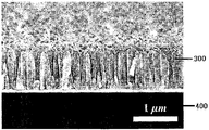
- FIG. 2 is a side scanning electron micrograph of a copper oxide nanostructure grown on a silicon substrate according to an experimental example of the present invention.
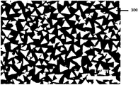
- FIG. 3 is a planar scanning electron micrograph of a copper oxide nanostructure grown on a silicon substrate according to another experimental example of the present invention.
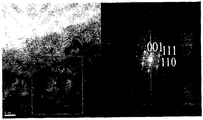
- FIG. 6 is a transmission electron micrograph of a copper oxide nanostructure according to another embodiment of the present invention.
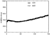
- FIG. 7 is a graph showing charge and discharge capacity of a lithium secondary battery used as a negative electrode by growing a copper oxide nanostructure on a copper current collector according to another embodiment of the present invention.
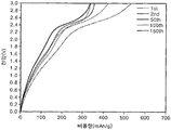
- FIG. 8 is a graph showing a charging curve when a current of 0.1 A / g is applied when a copper oxide nanostructure is used as a negative electrode to a lithium rechargeable battery in another embodiment of the present invention.
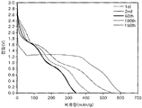
- FIG. 9 is a graph showing a discharge curve when a current of 0.1 A / g is applied when a copper oxide nanostructure is used as a cathode in a lithium rechargeable battery in another embodiment of the present invention.
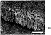
- FIG. 10 is a scanning micrograph showing the shape change of the copper oxide nanostructure after a single charge in another embodiment of the present invention.
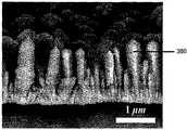
- FIG. 11 is a scanning micrograph showing the shape change of the copper oxide nanostructure after 100 charges in another embodiment of the present invention.
- FIG. 12 is a flowchart illustrating a method of manufacturing a nanostructure according to an experimental example of the present invention.
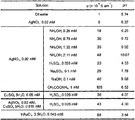
- 13 is a table showing the electrical conductivity and pH value of the electrolytic solution.
- FIG. 14 is a schematic diagram showing the growth behavior of the nanostructures using the reverse pulse coincidence mode by the method of manufacturing a nanostructure according to the present invention.
- 15 is a graph showing the relationship between the deposition time and the diameter and the scanning electron micrographs of the silver nanostructures grown using the reverse pulse coincidence mode by the method of manufacturing a nanostructure according to the present invention.
- 16 are scanning electron micrographs showing the growth behavior of the silver nanostructures grown using the reverse pulse coincidence mode according to the method of manufacturing a nanostructure according to the frequency change.
- 17 is a scanning electron micrograph showing the growth behavior of the silver nanostructures grown using the reverse pulse coincidence mode by the method of manufacturing a nanostructure according to the reduction voltage change.
- FIG. 18 is a scanning electron micrograph showing the growth behavior of the silver nanostructures grown using the reverse pulse coincidence mode by the method for manufacturing a nanostructure according to the present invention with respect to the electrical conductivity change of the electrolytic solution.
- the term “template” is used in the sense of defining an object having a property that can provide a particular preferential growth orientation with respect to the crystalline material growing thereon, while the term “substrate” refers to It is used in the sense of defining an object that does not provide a specific preferential growth orientation with respect to the crystalline material growing on the phase.
- “one-dimensional growth” means growing linearly in one direction.
- the “reduction voltage” means a voltage applied in a direction capable of providing electrons to a substrate on which the nanostructure is growing.
- the “oxidation voltage” refers to a voltage applied in the direction of removing electrons from the substrate on which the nanostructures are grown, and opposite to the reduction voltage.
- the present invention can provide a method for producing vertically grown nanostructures without using a template, and using a water-containing solution (referred to herein as a superdilution solution) containing a highly diluted electrolyte, one-dimensional of the nanostructures.
- a method of providing interfacial anisotropy for growth and providing a method of nucleating and growing a crystalline material from an electrolyte on a conductive substrate to form one-dimensional crystal grown nanostructures in a filamentary direction perpendicular to the conductive substrate. can be.
- FIG. 1 is a schematic diagram of a method for synthesizing a copper oxide nanostructure according to an embodiment of the present invention.
- the working electrode 100, the reference electrode 102, the counter electrode 104 are immersed in an electrolytic solution, a potentiostat (potentiostat),
- the copper oxide nanostructure may be formed on the working electrode 100 using the 200.
- the electrostatic potential device 200 applies a current between the counter electrode 104 and the working electrode 100, and the voltage applied to the working electrode 100 may be measured by setting the reference electrode 102 to 0V. Desired material from the electrolytic solution is deposited on the working electrode 100 as a nanostructure by the potential potential device 200. In addition, the electrostatic potential device 200 may change the magnitude and polarity of the voltage applied to the working electrode 100.
- the electrolyte solution may be a solution in which a material for forming a nanostructure (hereinafter, referred to as a material for forming a nanostructure) is dissolved, and may include an aqueous solution.
- the electrolytic solution may consist of a super-dilution electrolytic solution containing very small amounts of material for forming nanostructures.
- the electrolytic solution may include CuSO 4 .5H 2 O and H 2 SO 4 , for example CuSO 4 .5H 2 O in a range of 0.001 mM to 0.5 mM.
- the working electrode 100, the reference electrode 102 and the counter electrode 104 are immersed in a copper sulfate (CuSO 4 ) electrolytic solution, and the electrodes are potted on these electrodes (100, 102, 104).
- the pulse voltage may be applied in the potentiodynamic mode using the stat 200.
- Ag / AgCl is used as the reference electrode 102
- Pt mesh is used as the counter electrode 104
- copper foil or Si / Cr / Au wafer is used as the working electrode 100.
- the working electrode 100 for example, various conductive substrates having electrical conductivity may be used.
- the conductive substrate may be coated with a conductive material such as metal or carbon or doped with impurities so as to have electrical conductivity. In the present specification, it should be understood that the component described as the substrate corresponds to the working electrode 100.
- the copper oxide nano structure 300 may include copper oxide nanoparticles, copper oxide nanowires, copper oxide nanofibers, or copper oxide nanorods.
- the copper oxide nanostructure 300 may be formed in a moldless manner using such an electroplating method.
- the substrate 400 may include copper, stainless steel, nickel, silicon, gold, and the like.
- FIG. 2 is a scanning electron microscope photograph of one side of a copper oxide nanostructure 300 grown on a silicon substrate 400 according to another embodiment of the present invention
- FIG. 3 is a silicon substrate according to another embodiment of the present invention.
- the copper oxide nanostructure 300 is applied to a negative electrode for a lithium ion secondary battery.
- a copper oxide nanostructure may be formed on the negative electrode current collector.
- the negative electrode current collector is immersed in an electrolytic solution containing copper ions, and the copper oxide nano structure is grown on the negative electrode current collector by electroplating to form a negative electrode active material, thereby forming the copper oxide nano structure on the negative electrode current collector.
- the synthesized negative electrode can be prepared.
- the forming of the anode active material may be performed by directly growing the copper oxide nanostructure on the anode current collector without a template.
- Such a copper oxide nanostructure may extend upward from an upper surface of the negative electrode current collector.
- the negative electrode active material is directly formed on a substrate without using a binder, thereby simplifying the manufacturing process and reducing costs.
- Such a manufacturing process is performed at room temperature. It involves doing. Since the copper oxide nanostructures 300 may be grown on the substrate even at room temperature, the process of controlling the temperature may be omitted.
- the copper oxide nanostructure 300 is directly formed on the substrate.
- the copper oxide nanostructure 300 may include copper oxide nanoparticles, copper oxide nanowires, copper oxide nanofibers, or copper oxide nanorods.
- the copper oxide nanostructure 300 may include extending from the upper surface of the substrate to the upper portion.
- the copper oxide nano structure 300 may extend vertically upward from the top surface of the substrate.
- the copper oxide nanostructures 300 may further include growing apart from each other.
- the specific surface area and free space of the copper oxide nanostructures 300 are widened so that lithium ions are inserted into and removed from the copper oxide nanostructures.
- Copper oxide has high energy capacity compared to the conventional carbon-based negative electrode active material can be expected to improve the performance of the secondary battery. Furthermore, Cu 2 O is the most suitable negative electrode active material among the copper oxides of the present invention, and it can be expected to have an excellent effect compared to other copper oxides in terms of high specific capacity and volume expansion by charge and discharge.
- FIG. 4 is an X-ray diffraction analysis result of the copper oxide nano structure 300 grown on the silicon substrate according to another embodiment of the present invention
- Figure 5 is a growth on the copper current collector according to another embodiment of the present invention
- X-ray diffraction analysis of the copper oxide nanostructures 300 is shown.
- 6 is a transmission electron micrograph of the copper oxide nanostructure 300 according to another embodiment of the present invention.
- both the silicon current collector and the copper current collector in one embodiment of the electroplating method through the diffraction analysis curve of the copper oxide nano structure 300 grown on the silicon substrate and the copper current collector It can be seen that Cu 2 O was produced in.
- Cu 2 O is produced under the conditions shown in Table 1, and under different electroplating conditions, other 1 or 2 or more mixtures of copper oxides such as CuO, Cu 2 O 3 , CuO 2 and Cu 3 O 4, etc.
- the production may include copper oxide nanostructures in various forms such as nanowires, nanoparticles, nanofibers, nanorods, and the like.
- the copper oxide nanostructure may include a length of 0.1 ⁇ m to 500 ⁇ m grown on the substrate as needed.
- FIG. 7 is a graph showing charge and discharge capacity of a lithium secondary battery used as a negative electrode by growing a copper oxide nanostructure 300 on a copper current collector according to another embodiment of the present invention.
- 8 is a graph showing a charging curve when a current of 0.1 A / g is applied when the copper oxide nanostructure 300 is used as a negative electrode to a lithium rechargeable battery in another embodiment of the present invention.
- FIG. 9 is a graph showing a discharge curve when a current of 0.1 A / g is applied when the copper oxide nanostructure 300 is used as a cathode in a lithium rechargeable battery in another embodiment of the present invention.
- Charging and discharging of the lithium ion secondary batteries of FIGS. 7 to 9 were performed under the conditions shown in Table 2 below. Referring to Table 2, under this experimental condition, the voltage range was set to 0.001 to 3.0V, the applied current was set to 0.1 A / g, and the cycle characteristics were performed up to 150 cycles.
- FIG. 10 is a scanning microscope photograph showing the shape change of the copper oxide nanostructure 300 after one charge in another embodiment of the present invention.
- FIG. 11 is a scanning microscope photograph showing the shape change of the copper oxide nanostructure 300 after 100 charges in another embodiment of the present invention.
- the volume expansion change of the copper oxide nanostructure 300 after one charge and 100 charges of the lithium ion secondary battery can be confirmed.
- the volume expansion of the copper oxide nanostructure 300 is alleviated even when lithium ions are repeatedly inserted and detached in the charging and discharging process. You can see that.
- the present invention can provide a method for manufacturing a lithium ion secondary battery having improved lifespan by reducing deterioration of the negative electrode active material.
- the present invention can provide a secondary battery manufactured through the method of manufacturing a lithium ion secondary battery of the present invention.
- a lithium ion secondary battery may be formed using a method of manufacturing a lithium ion secondary battery, further comprising preparing a positive electrode and providing a separator interposed between the positive electrode and the negative electrode.
- the positive electrode may be formed of a positive electrode current collector and a positive electrode active material.
- a compound capable of reversible intercalation and deintercalation of lithium may be used.
- at least one of a complex oxide of metal and lithium selected from cobalt, manganese nickel, and combinations thereof may be used.
- microprocessed polyethylene microprocessed polypropylene, microprocessed polyvinylidene, microprocessed fluoride, or a multilayer film of two or more thereof may be used.
- the lithium ion secondary battery of the present invention includes a positive electrode made of a positive electrode current collector and a positive electrode active material formed on its surface, a negative electrode made of negative electrode current collector and a negative electrode active material formed on its surface, a separator interposed between the positive electrode and the negative electrode, the negative electrode
- a lithium ion secondary battery including copper nano water formed for a current collector can be provided.
- the negative electrode current collector may include any one of copper, stainless steel, and nickel.
- the copper oxide may include any one or a mixture of two or more selected from Cu 2 O, CuO, Cu 2 O 3 , CuO 2 , Cu 3 O 4 , and the negative electrode is cast-free in the negative electrode current collector. It can provide a lithium ion secondary battery comprising a formed.
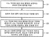
- FIG. 12 is a flowchart illustrating a method of manufacturing a nanostructure according to an experimental example of the present invention.
- the method of manufacturing a nanostructure may include providing a super-dilution electrolytic solution including a material for forming a nanostructure (S1); Immersing a conductive substrate (ie, an operating electrode) in the ultradilution electrolytic solution (S2); Applying a reduction voltage for providing electrons to the conductive substrate so as to deposit the nanostructure forming material on the conductive substrate to form a nanostructure (S3); And applying an oxidation voltage for removing electrons to the conductive substrate so as to dissolve at least a portion of the nanostructure deposited on the conductive substrate (S4).
- a super-dilution electrolytic solution including a material for forming a nanostructure (S1)
- Immersing a conductive substrate ie, an operating electrode
- an oxidation voltage for removing electrons to the conductive substrate so as to dissolve at least a
- the applying of the reducing voltage (S3) and the applying of the oxidation voltage (S4) may be performed alternately.
- the step of applying the reduction voltage (S3) and the step of applying the oxidation voltage (S4) for example, may be alternating with a frequency of 0.1 Hz to 10 Hz.
- this is exemplary and the case where the frequency is variously changed is included in the technical idea of the present invention.
- step S4 of applying the oxidation voltage may be omitted.
- the reduction voltage and the oxidation voltage may have opposite signs.
- the reduction voltage may be, for example, in the range of 1 V to 30 V, for example, in the range of 3 V to 20 V.
- the oxidation voltage may be, for example, in the range of ⁇ 0.01 V to ⁇ 5 V, for example, in the range of 0.1 V to 1 V.
- the ultra-dilution electrolytic solution may include the material for forming the nanostructure in the range of 0.001 mM to 0.5 mM.
- the material for forming the nanostructures may include at least one of a silver-containing material, a gold-containing material, and a copper-containing material.
- the superdilution electrolytic solution may have an electrical conductivity in the range of, for example, 1 ⁇ 10 ⁇ 6 S cm ⁇ 1 to 105 ⁇ 10 ⁇ 6 S cm ⁇ 1 , for example 23 ⁇ 10 ⁇ 6 S cm ⁇ 1 And electrical conductivity in the range from 105 ⁇ 10 ⁇ 6 S cm ⁇ 1 .
- the ultra-dilution electrolytic solution may include various auxiliary ionic materials to change the electrical conductivity.
- the auxiliary ionic material may not include the material for forming the nanostructure.
- the auxiliary ionic material may include, for example, at least one of NH 4 OH, Na 2 SO 4 , H 2 SO 4 , NaOH, and CH 3 COONH 4 .
- the ultra-dilution electrolytic solution may include the auxiliary ionic material in a range of 0.1 mM to 10 nM.
- the type and concentration of such auxiliary ionic materials are exemplary and the technical spirit of the present invention is not limited thereto.
- the electrical conductivity and pH value of the electrolytic solution 7 can change as these auxiliary ionic materials are added, as shown in FIG. 13.
- the nanostructure may include the material for forming the nanostructure.
- the nanostructures may have a diameter in the range of 80 nm to 800 nm, and may have an aspect ratio in the range of 2 to 10.
- the morphology of the nanostructures was observed using field emission scanning electron microscopy. Crystal structures of the nanostructures were analyzed using bright field transmission electron microscopy (BFTEM), high resolution transmission electron microscopy (HRTEM) and Energy Dispersive X-ray Spectroscopy (EDS).
- BFTEM bright field transmission electron microscopy
- HRTEM high resolution transmission electron microscopy
- EDS Energy Dispersive X-ray Spectroscopy
- the technical idea of the present invention is to provide the formation of a one-dimensional nanostructure in a super-dilution electrolytic solution that contains a very diluted diluted nanostructure forming material in the range 0.001 mM to 0.5 mM without using a template or a surfactant.
- One-dimensional nanostructures are nucleated as island shapes spaced apart from one another on a conductive substrate in a superdilution electrolytic solution. At the tips of the nucleated islands the electric field is locally increased, resulting in interfacial anisotropy. Such interfacial anisotropy causes islands to grow, respectively. This growth may be referred to as a lightning-rod effect, as it is similar to the lightning flowing through the lightning rod.
- ⁇ is the dielectric constant of the electrolytic solution
- ⁇ 0 is the dielectric constant of the vacuum
- l is the length of the nanostructure
- ⁇ is the radius of the end of the nanostructure
- ⁇ the electric field increasing factor
- ⁇ c the critical value
- ⁇ the critical value
- new nucleations occur such that branching or fractal growth occurs adjacent the ends.
- the critical value ⁇ c and the dielectric constant ⁇ of the electrolytic solution must be large. Since the dielectric constant ⁇ of the electrolytic solution is proportional to the log ( ⁇ ) of the electrolytic solution, the electrical conductivity ⁇ needs to be increased. For example, adding 0.1 mM Na 2 SO 4 auxiliary ionic material to the electrolytic solution, the electrical conductivity can be increased from 5x10 -6 S cm -1 to 29x10 -6 S cm -1 , and the aspect ratio can be increased to 5 Can be.
- One-dimensional growth of the nanostructures is driven by strong electric field enhanced interface anisotropy at the ends of the deposits after the deposits are nucleated as three-dimensional islands.
- the nanostructure formation method according to the present invention may be referred to as a filamentary one-dimensional nanocrystal growth in an ultra-dilute electrolyte (FONGUE) process.
- FONGUE ultra-dilute electrolyte
- the reverse pulsed coincidence mode where alternating reduction and oxidation voltages are applied, may form islands of uniformly sized nanostructures in the nucleation step. Since the islands do not occur simultaneously on the entire surface of the conductive substrate surface, the diameter distribution ⁇ d in the islands having the diameter d is made during one reduction-oxidation cycle of one reverse pulse at the nucleation density N. Lose.
- the nucleation density (N) is shown in Equation 2.
- N s is the density of the nucleus at saturation
- R n is the nucleation rate
- t is the reduction time
- R n is the nucleation rate and ⁇ is the overvoltage
- FIG. 14 is a schematic diagram showing the growth behavior of the nanostructures using the reverse pulse coincidence mode by the method of manufacturing a nanostructure according to the present invention.
- a method for producing a silver nanostructure is described, but the inventors have confirmed that the technical spirit of the present invention is not limited to this kind of material, for example, can be applied to a method for manufacturing a copper oxide nanostructure. .
- the growth behavior of the nanostructures is shown.
- fine nuclei having an average diameter d a and a diameter distribution ⁇ d are dispersed and formed on the conductive substrate.
- This nucleation is not governed by surface diffusion, but is governed by the precursor flux driven by the electric field to reach the surface of the conductive substrate because of the large random diffusion length of the silver atoms on the conductive substrate surface.
- the diffusion length is about 7 ⁇ m.
- nuclei having a smaller diameter than the critical diameter d c are dissolved and disappeared, while larger than the critical size d c .
- the nuclei with diameter remain.
- the remaining nuclei grow, and new nuclei nucleate and grow on a conductive substrate between the remaining nuclei.
- the growth rate of newly created nuclei is faster than the remaining nuclei, since the growth rate of the nucleus is inversely proportional to its size. Therefore, the density of the nucleus having a diameter larger than or equal to the critical diameter d c is increased as compared with the case of FIG. 14A.
- nuclei having a smaller diameter than the critical diameter d c are dissolved away, while compared to the critical size d c . Large diameter nuclei remain. As compared with the case of FIG. 14B, the density of the remaining nuclei is increased.
- islands of the nanostructure can be generated throughout the conductive substrate by repeated reduction and oxidation processes as described above, and a monolithic distribution of the islands on the conductive substrate. Can be promoted.
- the islands may have a relatively uniform size.
- nuclei are formed having a saturation diameter (d s ) and a saturation density (N s ).
- the saturation diameter (d s ) and the saturation density (N s ) are between the nucleation rate (R n ) and the growth rate (R g ) during one reverse pulse (ie, reduction and oxidation process) before the nucleation is saturated. Can be determined by competition. For example, if the nucleation rate (R n ) is larger than the growth rate (R g ), nucleation is dominant and saturated by smaller nuclei, resulting in larger saturation densities ( N s ) and smaller saturation diameter d s .
- the saturation diameter of nucleated and growing islands can be controlled by the diameter distribution ⁇ d and the average diameter d a of the nucleus formed during one reverse pulse.
- the diameter of the nanostructures can vary widely, for example the diameter can range from 80 nm to 800 nm.
- the value of the saturation diameter d s can be controlled by changing the frequency, the reduction voltage, and the electrical conductivity of the electrolytic solution. This will be described in detail below.
- 15 is a graph showing the relationship between the deposition time and the diameter and the scanning electron micrographs of the silver nanostructures grown using the reverse pulse coincidence mode by the method of manufacturing a nanostructure according to the present invention.
- the diameter of the nanostructure shows the S-shaped curve behavior with respect to log (t). It is also experimentally demonstrated that the saturation diameter of nucleated and growing nanostructures can be controlled by the diameter distribution ( ⁇ d) and the average diameter (d a ) of the nucleus formed during one reverse pulse.
- the saturation diameter of the nanostructure changes as the frequency changes.
- the circles show the nanostructures grown at a frequency of 0.25 Hz, the square is 0.5 Hz, the equilateral triangle is 1 Hz, and the inverted triangle is 5 Hz. As the frequency decreases, it can be seen that the saturation diameter of the nanostructure increases.
- 16 are scanning electron micrographs showing the growth behavior of the silver nanostructures grown using the reverse pulse coincidence mode according to the method of manufacturing a nanostructure according to the frequency change.
- the deposition time t until saturation increases, and the diameter of the nanostructure increases.
- the frequency was 0.25 Hz, it was saturated to a saturation diameter d s of 520 nm after 6 hours.
- the frequency was 0.5 Hz, after 1 hour, it was saturated to a saturation diameter (d s ) of 330 nm.
- the frequency was 1 Hz, it was saturated to a saturation diameter (d s ) of 200 nm after 30 minutes.
- the frequency was 5 Hz, after 20 minutes, it was saturated to a saturation diameter (d s ) of 80 nm.
- 17 is a scanning electron micrograph showing the growth behavior of the silver nanostructures grown using the reverse pulse coincidence mode by the method of manufacturing a nanostructure according to the reduction voltage change.
- Fig. 17 (a) is 7V (t is 2 hours 30 minutes), (b) is 10V (t is 1 hour 40 minutes), (c) is 14V (t is 1 hour), and (d) is 20V ( t is 1 hour).
- An electrolytic solution containing 0.02 mM AgNO 3 and 1.32 mM NH 4 OH was used for the deposition of the silver nanostructures. In all cases the frequency was fixed at 1 Hz.
- the average diameter d a of the nanostructure was linearly decreased from 270 nm to 140 nm.
- the average diameter by the increased voltage ( ⁇ ) by the increase in reduction potential (d a) and the size distribution during ( ⁇ d) can be varied.
- the average diameter d a and the diameter distribution ⁇ d of the nanostructures may be changed by the competition between the nucleation rate R n and the growth rate R g during one reverse pulse before saturation. Can be.
- the nucleation rate (R n ) can be controlled by changing the reduction voltage, the nucleation rate is proportional to exp (-1 / ⁇ 2 ) as shown in equation (3).
- the growth rate R g is proportional to the overvoltage ⁇ .
- FIG. 18 is a scanning electron micrograph showing the growth behavior of the silver nanostructures grown using the reverse pulse coincidence mode by the method for manufacturing a nanostructure according to the present invention with respect to the electrical conductivity change of the electrolytic solution.
- the electrical conductivity of the electrolytic solution is increased from 18 ⁇ 10 ⁇ 6 S cm ⁇ 1 to 48 ⁇ 10 ⁇ 6 S cm ⁇ 1 , and the The diameter increased from 190 nm to 330 nm. As the electrical conductivity of the electrolytic solution increases, the diameter of the nanostructures increases.
- auxiliary ionic material may be added to the electrolytic solution to change the electrical conductivity of the electrolytic solution.
- the auxiliary ionic material may use various materials, and may be, for example, NH 4 OH, H 2 SO 4 , NaOH, Na 2 SO 4 , or CH 3 COONH 4 .
- the auxiliary ionic material added to increase the electrical conductivity does not participate in the reduction reaction for deposition.
- the auxiliary ionic material carries most of the current in the electrolytic solution. This is because the concentration of auxiliary ionic material is relatively high compared to the concentration of silver (Ag) ions, which are electroactive precursor ions. Thus, the auxiliary ionic material reduces the electrical resistance of the electrolytic solution. In contrast, the auxiliary ionic material is nonelectroactive to the reduction reaction.
- the nucleation rate R n can be lower than the growth rate R g , whereby the growth of the nucleus predominates.
- the conductive substrate surface is covered with larger nuclei, the saturation diameter (d s ) of the nanostructure becomes larger and the saturation density (N s ) becomes smaller.
- the electrical conductivity of the electrolytic solution is increased, the growth of the nucleus is predominant, and the nanostructures have a larger saturation diameter (d s ), thereby realizing a nanostructure having a larger diameter.
- the increase in the electrical conductivity as the auxiliary ionic material is added to the electrolytic solution may lose the lightning rod effect, so that the electrical conductivity of the electrolytic solution needs to be controlled within the optimum range.
- the electrical conductivity of the electrolytic solution can be, for example, in the range 1 ⁇ 10 ⁇ 6 S cm ⁇ 1 to 105 ⁇ 10 ⁇ 6 S cm ⁇ 1 .
- silver nanostructures having a high aspect ratio of 5 to 8 may be implemented, which may be independent of the type of auxiliary ionic material. .
Landscapes
- Chemical & Material Sciences (AREA)
- Engineering & Computer Science (AREA)
- Chemical Kinetics & Catalysis (AREA)
- Electrochemistry (AREA)
- General Chemical & Material Sciences (AREA)
- Materials Engineering (AREA)
- Manufacturing & Machinery (AREA)
- Inorganic Chemistry (AREA)
- Metallurgy (AREA)
- Organic Chemistry (AREA)
- Battery Electrode And Active Subsutance (AREA)
- Cell Electrode Carriers And Collectors (AREA)
Abstract
본 발명은 주형 없이 경제적으로 기판 상에 구리산화물 나노 구조체를 제조할 수 있으면서 그 나노 구조체를 리튬이온 이차전지에 이용시 그 용량과 수명을 향상시키기 위하여 음극집전체를 구리 이온을 포함하는 전해용액에 침지시키는 단계 및 상기 전해용액에 침지된 상기 음극집전체 상에 전해도금법으로 구리산화물 나노 구조체를 성장시켜 음극 활물질을 형성하는 단계를 포함하는, 리튬이온 이차전지용 음극의 제조방법을 제공한다.
Description
본 발명은 나노 구조체의 제조방법에 관한 것으로서, 상세하게는 구리산화물 나노 구조체의 제조방법 및 이를 이용한 리튬이온 이차전지용 음극의 제조방법에 관한 것이다
리튬 이차 전지의 음극의 활물질은 주로 수명과 안정성 면에서 우수한 특성을 보이는 흑연이나 탄소가 상용화되어 사용되고 있다. 하지만, 이와 같은 탄소계 음극활물질은 이론에너지밀도가 372mAh/g에 해당하여 다른 금속 및 금속산화물을 기반으로 하는 음극활물질과 비교하여 상대적으로 매우 낮은 용량을 갖는 단점이 있다.
또한, 흑연이나 탄소를 음극활물질로 이용하는 리튬 이차 전지는 제조과정에서 바인더를 사용함으로써 공정이 복잡해지는 단점이 있다.
반면, 실리콘 및 주석 기반의 금속 및 금속산화물을 이용한 음극활물질은 이론에너지밀도가 700mAh/g이상으로 탄소계를 기반으로 하는 음극활물질보다 두 배 이상의 높은 에너지밀도를 갖지만, 부분 충전 또는 방전 시 리튬이온이 음극활물질내로 삽입 및 탈리하는 과정에서 300%이상의 부피 팽창을 유발하는 문제점을 가지고 있다. 이와 같은, 음극활물질의 부피 팽창은 재료 내에 스트레스가 쌓여 음극활물질의 기계적인 균열을 일으키고 결과적으로 리튬 이차 전지의 수명을 약화시키는 단점이 있다.
본 발명은 상기와 같은 문제점을 포함하여 여러 문제점들을 해결하기 위한 것으로서, 구리산화물 나노 구조체의 경제적인 제조방법과 이를 이용한 리튬 이차 전지용 음극의 경제적인 제조방법을 제공하는 것을 목적으로 하고 있다. 그러나 이러한 과제는 예시적인 것으로, 이에 의해 본 발명의 범위가 한정되는 것은 아니다.
본 발명의 일 관점에 따르면, 음극집전체를 구리 이온을 포함하는 전해용액에 침지시키는 단계; 및 상기 전해용액에 침지된 상기 음극집전체 상에 전해도금법으로 구리산화물 나노 구조체를 성장시켜 음극 활물질을 형성하는 단계; 를 포함하는, 리튬이온 이차전지용 음극의 제조방법을 제공한다.
상기 리튬이온 이차전지용 음극의 제조방법에 있어서, 상기 음극 활물질을 형성하는 단계는 상기 음극집전체 상에 상기 구리산화물 나노 구조체를 주형(template)없이 직접 성장시키는 단계를 포함할 수 있다.
상기 리튬이온 이차전지용 음극의 제조방법에 있어서, 상기 구리산화물 나노 구조체는 구리산화물 나노입자, 구리산화물 나노와이어, 구리산화물 나노섬유 또는 구리산화물 나노로드를 포함할 수 있다.
상기 리튬이온 이차전지용 음극의 제조방법에 있어서, 상기 구리산화물 나노 구조체는 상기 음극집전체의 상면에서 상부로 신장할 수 있다.
상기 리튬이온 이차전지용 음극의 제조방법에 있어서, 상기 구리산화물 나노 구조체는 성장 길이가 0.1μm 내지 500 μm 일 수 있다.
상기 리튬이온 이차전지용 음극의 제조방법에 있어서, 상기 구리산화물 나노 구조체는 Cu2O, CuO, Cu2O3, CuO2 및 Cu3O4로 이루어진 군에서 선택되는 어느 하나 또는 2 이상의 혼합물을 포함할 수 있다.
상기 리튬이온 이차전지용 음극의 제조방법에 있어서, 상기 음극집전체는 구리, 스텐레스 스틸 또는 니켈을 포함할 수 있다.
상기 리튬이온 이차전지용 음극의 제조방법에 있어서, 상기 전해도금법은 상온에서 수행될 수 있다.
본 발명의 다른 관점에 따르면, 기판을 구리 이온을 포함하는 전해용액에 침지시키는 단계; 및 전해도금법으로 상기 전해용액으로부터 상기 기판 상에 구리 이온을 공급하여 상기 기판 상에 구리산화물 나노 구조체를 성장시키는 단계; 를 포함하는, 구리산화물 나노 구조체를 제공할 수 있다.
상기 구리산화물 나노 구조체에 있어서, 상기 전해용액은 황산구리 용액을 포함하고, 상기 전해도금법은 동전위(potentiodynamic) 모드로 수행될 수 있다.
상기 구리산화물 나노 구조체에 있어서, 상기 침지시키는 단계는, 상기 전해용액 내에 Ag/AgCl 기준전극을 침지하는 단계; 및 상기 전해용액 내에 Pt 메쉬 대항전극을 침지하는 단계를 더 포함할 수 있다.
상기한 바와 같이 이루어진 본 발명의 일 실시예에 따르면, 주형 없이 경제적으로 기판 상에 구리산화물 나노 구조체를 제조할 수 있다. 나아가, 이러한 구리산화물 나노 구조체을 리튬이온 이차전지용 음극으로 이용함으로써, 리튬이온 이차전지의 충방전시 부피변화를 크게 하지 않으면서 그 용량과 수명을 향상시키고, 그 제조공정을 단순화할 수 있다.
본 발명의 효과는 이상에서 언급한 것으로 제한되지 않으며, 언급되지 않은 또 다른 효과들은 아래의 기재로부터 본 발명이 속하는 기술 분야의 통상의 지식을 가진 자에게 명확하게 이해될 수 있을 것이다.
도 1은 본 발명의 일 실시예에 따른 구리산화물 나노 구조체를 합성하기 위한 전해도금법을 설명하기 위한 개략도 이다.
도 2는 본 발명의 일 실험예에 따라 실리콘 기판 위에 성장된 구리산화물 나노 구조체의 측면 주사전자현미경 사진이다.
도 3은 본 발명의 다른 실험예에 따라 실리콘 기판 위에 성장된 구리산화물 나노 구조체의 평면 주사전자현미경 사진이다.
도 4는 본 발명의 또 다른 실시예에 따른 실리콘 기판 위에 성장된 구리산화물 나노 구조체의 X 선 회절분석 결과 그림이다.
도 5는 본 발명의 또 다른 실시예에 따른 구리 집전체 위에 성장된 구리산화물 나노 구조체의 X 선 회절 분석 결과 그림이다.
도 6은 본 발명의 또 다른 실시예에 따른 구리산화물 나노 구조체의 투과전자현미경 사진이다.
도 7은 본 발명의 또 다른 실시예에 따른 구리 집전체 위에 구리 산화물 나노 구조체를 성장시켜 음극으로 사용한 리튬이차전지의 충방전 용량을 나타내는 그래프이다.
도 8은 본 발명의 또 다른 실시예에서 구리산화물 나노 구조체를 리튬이자전지에 음극으로 사용시 0.1A/g의 전류를 인가했을 때의 충전 곡선을 나타내는 그래프이다.
도 9는 본 발명의 또 다른 실시예에서 구리산화물 나노 구조체를 리튬이자전지에 음극으로 사용시 0.1A/g의 전류를 인가했을 때의 방전 곡선을 나타내는 그래프이다.
도 10은 본 발명의 또 다른 실시예에서 1회 충전 후의 구리산화물 나노 구조체의 모양 변화를 나타내는 주사현미경 사진이다.
도 11은 본 발명의 또 다른 일 실시예에서 100회 충전 후의 구리산화물 나노 구조체의 모양 변화를 나타내는 주사현미경 사진이다.
도 12는 본 발명의 실험예에 따른 나노 구조체의 제조 방법을 설명하는 흐름도이다.
도 13은 전해 용액의 전기 전도도 및 pH 값을 나타내는 표이다.
도 14는 본 발명에 따른 나노 구조체의 제조 방법에 의한 역 펄스 동전위 모드를 이용한 나노 구조체의 성장 거동을 나타내는 모식도이다.
도 15는 본 발명에 따른 나노 구조체의 제조 방법에 의한 역 펄스 동전위 모드를 이용하여 성장한 은 나노 구조체의 증착 시간과 직경의 관계 및 주사전자 현미경 사진들을 나타내는 그래프이다.
도 16은 본 발명에 따른 나노 구조체의 제조 방법에 의한 역 펄스 동전위 모드를 이용하여 성장한 은 나노 구조체의 성장 거동을 주파수 변화에 대하여 나타내는 주사전자현미경 사진들이다.
도 17은 본 발명에 따른 나노 구조체의 제조 방법에 의한 역 펄스 동전위 모드를 이용하여 성장한 은 나노 구조체의 성장 거동을 환원 전압 변화에 대하여 나타내는 주사전자현미경 사진들이다.
도 18은 본 발명에 따른 나노 구조체의 제조 방법에 의한 역 펄스 동전위 모드를 이용하여 성장한 은 나노 구조체의 성장 거동을 전해 용액의 전기 전도도 변화에 대하여 나타내는 주사전자현미경 사진들이다.
이하, 첨부된 도면들을 참조하여 본 발명의 실시예를 상세히 설명하면 다음과 같다. 그러나 본 발명은 이하에서 개시되는 실시예에 한정되는 것이 아니라 서로 다른 다양한 형태로 구현될 수 있는 것으로, 이하의 실시예는 본 발명의 개시가 완전하도록 하며, 통상의 지식을 가진 자에게 발명의 범주를 완전하게 알려주기 위해 제공되는 것이다. 또한 설명의 편의를 위하여 도면에서는 구성 요소들이 그 크기가 과장 또는 축소될 수 있다.
본 명세서에서 전체적으로, 용어 "템플릿(template)"은 그 상에 성장하는 결정 물질에 대하여 특정한 우선 성장 방위를 제공할 수 있는 특성을 가지는 물체를 한정하는 의미로 사용되며, 반면 용어 "기판"은 그 상에 성장하는 결정 물질에 대하여 특정한 우선 성장 방위를 제공하지 않는 물체를 한정하는 의미로 사용된다. 또한, "일차원 성장"은 일방향으로 선형(linear)으로 성장하는 것을 의미한다. 또한, "환원 전압"은 나노 구조체가 성장하는 기판에 전자를 제공할 수 있는 방향으로 인가되는 전압을 의미한다. 반면, "산화 전압"은 나노 구조체가 성장하는 기판으로부터 전자를 제거하는 방향으로 인가되는 전압을 의미하고, 상기 환원 전압과는 방향이 반대이다.
본 발명은 템플릿을 사용하지 않고 수직 성장된 나노 구조체를 제조하는 방법을 제공할 수 있으며, 매우 희석된 전해질을 포함하는 수분 함유 용액(본 명세서에서는 초희석 용액으로 지칭함)을 이용하여 나노 구조체의 일차원 성장을 위한 계면 이방성을 제공하고, 전해질로부터 결정 물질이 전도성 기판 상에 핵생성 및 성장하여 상기 전도성 기판에 대하여 수직 방향으로 필라멘트형(filamentary)으로 일차원 결정 성장된 나노 구조체들을 형성하는 방법을 제공할 수 있다.
도 1은 본 발명의 일 실시예에 따른 구리산화물 나노 구조체를 합성하는 방법에 대한 개략도이다.
도 1을 참조하면, 작동전극(working electrode, 100), 기준전극(reference electrode, 102), 대항전극(counter electrode, 104)을 전해용액에 침지시킨 후에 정전위 장치(포텐쇼스탯(potentiostat), 200)을 사용하여 작동전극(100) 상에 구리산화물 나노 구조체를 형성할 수 있다.
정전위 장치(200)는 대항전극(104)과 작동전극(100) 사이에 전류를 인가하고, 작동전극(100)에 인가되는 전압은 기준전극(102)을 0V로 설정하여 측정될 수 있다. 정전위 장치(200)에 의하여 전해용액으로부터 원하는 물질이 나노 구조체로서 작동전극(100)에 증착된다. 또한, 정전위 장치(200)는 작동전극(100)에 인가되는 전압의 크기와 극성을 변화시킬 수 있다.
전해용액은 나노 구조체를 형성하기 위한 물질(이하에서는 나노 구조체 형성 대상 물질로 지칭함)이 용해된 용액일 수 있고, 수용액을 포함할 수 있다. 전해 용액은 나노 구조체를 형성하기 위한 물질을 매우 적은 양으로 포함하는 초희석 전해 용액으로 구성될 수 있다. 예를 들어, 구리 나노 구조체를 형성하는 경우에는, 전해 용액은 CuSO4ㆍ5H2O 및 H2SO4을 포함할 수 있고, 예를 들어 0.001 mM 내지 0.5 mM 범위로 CuSO4ㆍ5H2O을 포함할 수 있고, 예를 들어 약 0.05 mM 로 CuSO4ㆍ5H2O을 포함할 수 있고, 예를 들어 0.001 mM 내지 0.5 mM 범위로 H2SO4을 포함할 수 있고, 예를 들어 약 0.026 mM 로 H2SO4을 포함할 수 있다.
구리산화물 나노 구조체를 형성하기 위한 전해도금의 예시적인 공정조건은 표 1에 제시된 바와 같다.
표 1 
표 1에 도시된 바와 같이, 황산구리(CuSO4) 전해용액 내에 작동전극(100), 기준전극(102) 및 대항전극(104)을 침지시키고, 이들 전극들(100, 102, 104)에 포텐쇼스탯(200)을 이용하여 동전위 모드(potentiodynamic mode)로 펄스 전압을 인가할 수 있다. 예를 들어, 기준전극(102)으로 Ag/AgCl이 사용되고, 대항전극(104)으로 백금 메쉬(Pt mesh)가 사용되고, 작동전극(100)으로 구리 포일(Cu foil) 또는 Si/Cr/Au 웨이퍼가 사용될 수 있다. 작동전극(100)은, 예를 들어 전기전도성을 가지는 다양한 전도성 기판을 사용할 수 있다. 상기 전도성 기판은 전기전도성을 가지도록 표면에 금속이나 탄소와 같은 전도성 물질이 코팅되거나 불순물이 도핑될 수 있다. 본 명세서에서, 기판으로 기재되는 구성 요소는 작동전극(100)에 상응함을 이해하여야 한다.
이에 따르면, 전해용액으로부터 구리이온을 공급하여, 별도의 주형(template)을 사용하지 않고 전해도금법으로 작동전극(100) 상에 구리산화물 나노 구조체를 성장시킬 수 있다. 예를 들어, 이러한 구리산화물 나노 구조체(300)는 구리산화물 나노입자, 구리산화물 나노와이어, 구리산화물 나노섬유 또는 구리산화물 나노로드를 포함할 수 있다.
나아가, 작동전극으로 다양한 기판(400)이 이용될 수 있다는 점을 감안하면, 이러한 전해도금법을 이용하여 무주형으로 구리산화물 나노 구조체(300)를 형성할 수 있게 된다. 예를 들어, 이러한 기판(400)은 구리, 스테인레스 스틸, 니켈, 실리콘, 금 등을 포함할 수 있다.
도 2은 본 발명의 다른 일 실시예에 따른 실리콘 기판(400) 위에 성장된 구리산화물 나노 구조체(300) 일 측면의 주사전자현미경 사진이고, 도 3은 본 발명의 다른 일 실시예에 따른 실리콘 기판 위에 상장된 구리산화물 나노 구조체(300)의 평면의 주사전자현미경 사진이다.
이러한 전해도금법을 이용하면, 도 2 및 도 3에 도시된 바와 같이, 실리콘 기판위에 구리산화물 나노 구조체(300)들이 실리콘 기판 상방으로 조밀하게 형성된 것을 알 수 있다.
이하에서는 이러한 구리산화물 나노 구조체(300)를 리튬이온 이차전지용 음극에 응용하는 실시예에 대해서 설명한다.
전술한 도 1의 설명을 참조하여, 기판으로 음극집전체를 이용하면, 음극집전체 상에 구리산화물 나노 구조체를 형성할 수 있다. 예를 들어, 음극집전체를 구리 이온을 포함하는 전해용액에 침지시키고, 이러한 음극집전체 상에 전해도금법으로 구리산화물 나노 구조체를 성장시켜 음극 활물질을 형성함으로써, 음극집전체 상에 구리산화물 나노 구조체가 합성된 음극을 제조할 수 있다. 여기에서, 음극 활물질을 형성하는 단계는 음극집전체 상에 상기 구리산화물 나노 구조체를 주형(template)없이 직접 성장시켜 수행할 수 있다. 이러한 구리산화물 나노 구조체는 음극집전체의 상면에서 상부로 신장할 수 있다.
전술한 표 1과 같은 조건에 의할 경우 바인더를 사용하지 않고 음극활물질을 기판 상에 직접 형성시켜, 제조 공정을 단순화 하고, 비용을 절감할 수 있는 장점이 있으며, 이와 같은 제조 공정은 상온에서 실시하는 것을 포함한다. 상온에서도 기판 위에 구리산화물 나노 구조체(300)를 성장하는 것이 가능하여, 온도를 제어하여야 하는 공정을 생략할 수 있다.
이와 같은 제조 공정에 의할 경우 기판에 구리산화물 나노 구조체(300)가 직접 형성되는 것을 확인할 수 있다. 이 때, 구리산화물 나노 구조체(300)는 구리산화물 나노입자, 구리산화물 나노와이어, 구리산화물 나노섬유 또는 구리산화물 나노로드를 포함할 수 있다.
또한, 구리산화물 나노 구조체(300)는 기판의 상면에서 상부로 신장하는 것을 포함할 수 있다. 예를 들어, 구리산화물 나노 구조체(300)는 기판의 상면에서 수직 상방으로 신장할 수 있다. 더 나아가, 구리산화물 나노 구조체(300)가 상부로 신장하는 경우 복수의 구리산화물 나노 구조체(300)가 서로 이격하여 성장하는 것을 더 포함할 수 있다.
복수의 구리산화물 나노 구조체(300)가 서로 이격하여 밀집된 형상으로 성장할 경우 구리산화물 나노 구조체(300)의 비표면적과 자유공간을 넓혀, 리튬이온이 구리산화물 나노 구조체 내로 삽입 및 탈리하는 과정에서 발생하는 부피팽창에 의한 스트레스를 완화시킬 수 있을 뿐 아니라 리튬이온의 저장 공간을 늘릴 수 있고 결과적으로 충전 용량을 늘릴 수 있어 이차전지의 성능을 향상시킬 수 있는 효과를 기대할 수 있다.
구리 산화물은 기존의 탄소계 음극활물질에 비하여 에너지 용량이 높아 이차전지의 성능을 향상시킬 수 있는 있는 효과를 기대할 수 있다. 더 나아가, 본 발명의 구리 산화물 중 Cu2O가 가장 적합한 음극활물질이며, 비용량이 높고 충방전에 의한 부피팽창에 있어 다른 구리산화물에 비하여 우수한 효과를 기대할 수 있다.
도 4는 본 발명의 또 다른 실시예에 따른 실리콘 기판 위에 성장된 구리산화물 나노 구조체(300)의 X 선 회절분석 결과 그림이고, 도 5는 본 발명의 또 다른 실시예에 따른 구리 집전체 위에 성장된 구리산화물 나노 구조체(300)의 X 선 회절 분석 결과 그림이다. 또한, 도 6은 본 발명의 또 다른 실시예에 따른 구리산화물 나노 구조체(300)의 투과전자현미경 사진이다.
도 4, 도 5 및 도 6을 참조하면, 실리콘 기판과 구리 집전체에 성장된 구리산화물 나노 구조체(300)의 회절 분석 곡선을 통해 전해도금 방식의 일 실시예에서 실리콘 집전체 및 구리 집전체 모두에서 Cu2O를 생성했음을 확인할 수 있다.
Cu2O는 표 1의 조건하에서, 생성되며 그 외 전해도금 방식의 조건을 달리하면, 그 외 CuO, Cu2O3, CuO2 및 Cu3O4 등과 같은 구리산화물의 하나 또는 2 이상의 혼합물의 생성을 포함할 수 있고, 구리 산화물 나노 구조체는 나노선, 나노입자, 나노섬유, 나노로드 등의 다양한 형태가 가능하다.
또한, 구리 산화물 나노 구조체는 필요에 따라 기판상부에 성장된 길이가 0.1μm 내지 500μm 인 것을 포함할 수 있다.
도 7은 본 발명의 또 다른 실시예에 따른 구리 집전체 위에 구리 산화물 나노 구조체(300)를 성장시켜 음극으로 사용한 리튬이차전지의 충방전 용량을 나타내는 그래프이다. 도 8은 본 발명의 또 다른 실시예에서 구리산화물 나노 구조체(300)를 리튬이자전지에 음극으로 사용시 0.1A/g의 전류를 인가했을 때의 충전 곡선을 나타내는 그래프이다. 도 9는 본 발명의 또 다른 실시예에서 구리산화물 나노 구조체(300)를 리튬이자전지에 음극으로 사용시 0.1A/g의 전류를 인가했을 때의 방전 곡선을 나타내는 그래프이다.
도 7 내지 도 9의 리튬이온 이차전지의 충방전은 하기의 표 2의 조건하에서 실시하였다. 표 2를 참조하면, 본 실험 조건에서 전압 범위(voltage range)는 0.001 내지 3.0V로 하였고, 인가 전류(applied current)는 0.1A/g으로 하였고, 사이클 특성은 150 사이클까지 진행하였다.
표 2
도 7 내지 도 9를 참조하면, 충전시와 방전시 충전사이클 회수의 변화에 관계없이 비용량이 거의 일치되는 것을 확인할 수 있으며, 이를 통해 전류 효율이 100%에 가까운 것을 알 수 있다.
도 10은 본 발명의 또 다른 실시예에서 1회 충전 후의 구리산화물 나노 구조체(300)의 모양 변화를 나타내는 주사현미경 사진이다. 도 11은 본 발명의 또 다른 일 실시예에서 100회 충전 후의 구리산화물 나노 구조체(300)의 모양 변화를 나타내는 주사현미경 사진이다.
도 10 및 도 11을 참조하면, 리튬이온 이차전지의 1회 충전과 100회 충전후의 구리 산화물 나노 구조체(300)의 부피 팽창 변화를 확인할 수 있다.
이때, 본 발명은 구리산화물 나노 구조체(300)를 전해도금 방식으로 음극집전체에 직접 성장시키는 경우 리튬이온이 충방전 과정에서 삽입과 탈리를 반복하더라도 구리산화물 나노 구조체(300)의 부피 팽창이 완화되는 것을 확인할 수 있다.
결과적으로, 본 발명은 음극활물질의 열화를 줄여 수명이 개선된 리튬이온 이차전지 제조방법을 제공할 수 있다.
더 나아가, 본 발명의 또 다른 일 실시예로 본 발명의 리튬이온 이차전지의 제조방법을 통해 제조된 이차전지를 제공할 수 있다.
구체적으로 검토하면, 양극을 준비하는 단계 및 상기 양극과 상기 음극 사이에 개재되는 세퍼레이터를 구비하는 단계를 더 포함하는 리튬이온 이차전지 제조방법을 이용하여 리튬이온 이차전지를 형성할 수 있다.
양극은 양극집전체와 양극활물질로 형성될 수 있다. 양극활물질로는 리튬의 가역적인 인터칼레이션 및 디인터칼레이션이 가능한 화합물을 사용할 수 있다. 구체적으로 코발트, 망간 니켈, 및 이들의 조합으로부터 선택되는 금속과 리튬과의 복합 산화물 중 1종 이상의 것을 사용할 수 있다.
세퍼레이터(separator)로는 미소공정 폴리에틸렌, 미소공정 폴리프로필렌, 미소공정 폴리비닐리엔, 미소공정 플루오사이드 또는 이들의 2층 이상의 다층막이 사용될 수도 있다.
본 발명을 효과를 구현하기 위한 일 실시예는 하기의 표 3의 조건과 같다.
표 3 
본 발명의 리튬이온 이차전지는 양극집전체와 그 표면에 형성되는 양극활물질로 된 양극, 음극집전체와 그 표면에 형성되는 음극활물질로 된 음극, 상기 양극과 음극 사이에 개재되는 세퍼레이터, 상기 음극집전체 위해 형성된 구리나노물을 포함하는 리튬이온 이차전지를 제공할 수 있다.
또한, 상기 음극집전체는 구리, 스테인레스 스틸, 니켈 중의 어느 하나를 포함할 수 있다.
더 나아가, 상기 구리산화물은 Cu2O, CuO, Cu2O3, CuO2, Cu3O4에서 선택되는 어느 하나 또는 2 이상의 혼합물을 포함할 수 있으며, 상기 음극은 상기 음극집전체에 무주형으로 형성되는 것을 포함하는 리튬이온 이차전지를 제공할 수 있다.
이하에서는 상술한 내용을 바탕으로 나노 구조체의 성장 메카니즘과 나노 구조체의 제조방법 등의 기술적 특징을 본 발명의 실험예 등에 의하여 구체적으로 설명한다. 다만, 본 발명의 실험예들은 당해 기술 분야에서 통상의 지식을 가진 자에게 본 발명의 기술적 사상을 더욱 완전하게 설명하기 위하여 제공되는 것이며, 본 발명의 기술적 사상의 범위가 하기 실험예 등에 한정되는 것은 아니다.
나노 구조체의 제조방법
도 12는 본 발명의 실험예에 따른 나노 구조체의 제조 방법을 설명하는 흐름도이다.
도 12를 참조하면, 나노 구조체의 제조 방법은, 나노 구조체 형성 대상 물질을 포함하는 초희석 전해 용액을 제공하는 단계(S1); 상기 초희석 전해 용액 내에 전도성 기판(즉, 작동 전극)을 침지하는 단계(S2); 상기 나노 구조체 형성 대상 물질을 상기 전도성 기판에 증착시켜 나노 구조체를 형성하도록, 상기 전도성 기판에 전자를 제공하는 환원 전압을 인가하는 단계(S3); 및 상기 전도성 기판에 증착된 상기 나노 구조체의 적어도 일부를 용해시키도록, 상기 전도성 기판에 전자를 제거하는 산화 전압을 인가하는 단계(S4);를 포함한다.
상기 환원 전압을 인가하는 단계(S3)와 상기 산화 전압을 인가하는 단계(S4)는 교대로 수행될 수 있다. 예를 들어, 상기 환원 전압을 인가하는 단계(S3)와 상기 산화 전압을 인가하는 단계(S4)는, 예를 들어 0.1 Hz 내지 10 Hz의 주파수를 가지고 교번될 수 있다. 그러나, 이는 예시적이며, 상기 주파수가 다양하게 변화되는 경우도 본 발명의 기술적 사상에 포함된다. 대안적으로, 상기 산화 전압을 인가하는 단계(S4)는 생략될 수 있다.
상술한 바와 같이, 상기 환원 전압과 상기 산화 전압은 서로 반대의 부호를 가질 수 있다. 상기 환원 전압은, 예를 들어 1 V 내지 30 V 범위일 수 있고, 예를 들어 3 V 내지 20 V 범위일 수 있다. 상기 산화 전압은, 예를 들어 -0.01 V 내지 -5 V 범위일 수 있고, 예를 들어 0.1 V 내지 1 V 범위일 수 있다.
상기 초희석 전해 용액은 상기 나노 구조체 형성 대상 물질을 0.001 mM 내지 0.5 mM 범위로 포함할 수 있다. 상기 나노 구조체 형성 대상 물질은 은 함유 물질, 금 함유 물질, 및 구리 함유 물질 중 적어도 어느 하나를 포함할 수 있다.
상기 초희석 전해 용액은, 예를 들어 1 x 10⁻⁶ S cm-1 내지 105 x 10-6 S cm-1 범위의 전기 전도도를 가질 수 있고, 예를 들어 23 x 10-6 S cm-1 내지 105 x 10-6 S cm-1 범위의 전기 전도도를 가질 수 있다.
상기 초희석 전해 용액은, 전기 전도도를 변화시키기 위하여, 다양한 보조 이온 물질을 포함할 수 있다. 상기 보조 이온 물질은 상기 나노 구조체 형성 대상 물질을 포함하지 않을 수 있다. 상기 보조 이온 물질은, 예를 들어 NH4OH, Na2SO4, H2SO4, NaOH, 및 CH3COONH4 중 적어도 어느 하나를 포함할 수 있다. 상기 초희석 전해 용액은 상기 보조 이온 물질을 0.1 mM 내지 10 nM 범위로 포함할 수 있다. 그러나, 이러한 보조 이온 물질의 종류와 농도는 예시적이며 본 발명의 기술적 사상은 이에 한정되는 것은 아니다. 전해 용액(7)의 전기 전도도 및 pH 값은 이러한 보조 이온 물질이 추가됨에 따라 변화될 수 있고, 도 13과 같다.
상기 나노 구조체는 상기 나노 구조체 형성 대상 물질을 포함할 수 있다. 상기 나노 구조체는 80 nm 내지 800 nm 범위의 직경을 가질 수 있고, 2 내지 10 범위의 종횡비를 가질 수 있다.
나노 구조체의 전기화학적 분석 방법 및 미세 구조 분석 방법
나노 구조체의 모폴로지를 전계 방출 주사 전자 현미경을 이용하여 관찰하였다. 나노 구조체의 결정 구조들은 명시야 투과전자현미경(bright field transmission electron microscopy, BFTEM), 고해상도 투과전자현미경(high resolution transmission electron microscopy, HRTEM) 및 EDS(Energy Dispersive X-ray Spectroscopy)를 이용하여 분석하였다.
순환 전압 전류 곡선(Cyclic voltammogram)을 얻기 위하여, 동전위 전기화학 시스템을 이용하여 전해 용액에 -14 V 내지 2 V의 범위의 전압을 인가하여 50 mV/s의 스캔 속도로 측정을 수행하였다.
통상적인 전도도 측정 시스템을 이용하여 상기 전해 용액의 전기 전도도 및 pH를 측정하였다. 그 결과는 도 13과 같다.
일차원 나노 구조체의 형성
본 발명의 기술적 사상은 템플릿이나 계면 활성제를 사용하지 않고, 나노 구조체 형성 대상 물질을 0.001 mM 내지 0.5 mM 범위로 매우 희석되어 포함하는 초희석 전해 용액 내에서의 일차원 나노 구조체의 형성을 제공하는 것이다.
일차원 나노 구조체들은 초희석 전해 용액 내에서 전도성 기판 상에 서로 이격된 아일랜드 형상으로서 핵생성된다. 상기 핵생성된 아일랜드들의 말단(tip)들에서는 전기장이 국부적으로 증대되며, 이에 따라 계면 이방성이 야기된다. 이러한 계면 이방성에 의하여 아일랜드들이 각각 성장한다. 이러한 성장은 피뢰침에 번개가 집중되어 흐르는 것과 유사하므로, 피뢰침 효과(lightening-rod effect)로 지칭될 수 있다.
이미 오래전에, 비-평형 상태에서, 예를 들어 파세트형(facet) 결정 구조들, 바늘형 결정 구조들, 수지상정형(dendritic) 결정 구조들 및 프랙탈형(fractal) 결정 구조들과 같은 거시적인 구조들에 대한 성장은 전기 화학 분야에서 주요한 연구 과제이었다. 이러한 성장은, 확산 집합체(diffusion-limited aggregation, DLA) 및 멀린스-세케르카(Mullins-Sekerka) 모폴로지 불안정성 특성 등을 통하여 이해되었고, 성장하는 결정 구조체의 계면이 불안정함을 증명되었다. 고상과 액상 사이의 계면 이방성이 높은 경우에는, 방향성을 가지고 분지되는 수지상정형 성장이 우선되는 것으로 알려져 있다. 반면, 고상과 액상 사이의 계면 이방성이 낮은 경우에는, 무작위로 분지되는 프랙탈 성장이 우선되는 것으로 알려져 있다. 결정 구조체가 전기-증착되는 동안에, 성장하는 결정 구조체의 말단들 주위에서 전기-대류(electro-convection)가 발생하며, 이는 상기 말단들에서 전하들이 가는 분지들 사이의 용액들 내에 대류됨을 의미한다. 따라서, 말단들에서의 국부적인 전기장은 전해질의 전체 전기장에 비하여 크게 되고, 이에 따라 상술한 피뢰침 효과가 야기될 수 있다.
일차원 나노 구조체의 성장 메카니즘
이하에서는, 본 발명의 제조 방법에 이용하여 형성한 일차원 나노 구조체의 성장 메카니즘에 대하여 설명하기로 한다.
전해 용액으로부터 구리산화물이 환원 전압에 의하여 전자를 제공받아 전도성 기판에 증착되며, 이러한 구리산화물 증착물은 전도성 기판 상에 반구형 아일랜드들로 핵생성한다. 이어서, 상기 반구형 아일랜드들의 볼록한 말단들에서 전해 용액 방향으로 필라멘트형 일차원 성장이 이루어진다. 이러한 일차원 성장은 초희석 전해 용액 내에서 아일랜드들의 종횡비에 의하여 전기장이 국부적으로 강화되기 때문이다. 이는 피뢰침의 볼록한 부분에 집중되는 피뢰침 효과와 유사하다. 이와 같은 전기장 증대 인자(β)는 수학식 1과 같다.
수학식 1 
(여기에서, ε는 전해 용액의 유전 상수, ε0는 진공의 유전 상수, l은 나노 구조체의 길이, ρ 는 나노 구조체의 말단의 반경임)
전기장 증대 인자(β)가 임계 수치(βc)에 도달하면, 나노 구조체의 성장 말단에 급격하게 증가된 과전압(η)이 걸리게 되고, 상기 말단에 인접한 영역에 새로운 핵이 형성되는 것으로 해석될 수 있다. 예를 들어, 정전위 모드에서 나노 구조체의 종횡비가 약 2 이상인 경우에는, 상기 말단에 인접하여 분지 성장 또는 프랙탈 성장이 이루어지도록 새로운 핵생성들이 발생한다.
나노 구조체의 종횡비가 증가되기 위하여는, 즉, 더 길고 얇은 나노 구조체를 얻기 위해서는, 임계 수치(βc)와 전해 용액의 유전 상수(ε)가 커져야 한다. 전해 용액의 유전 상수(ε)는 전해 용액의 log(σ)에 전체적으로 비례하므로, 전기 전도도(σ)가 증가될 필요가 있다. 예를 들어, 0.1 mM Na2SO4 보조 이온 물질을 전해 용액에 추가하면, 전기 전도도는 5x10⁻⁶ S cm-1에서 29x10-6 S cm-1로 증가될 수 있고, 종횡비는 5까지 증가될 수 있다. 나노 구조체의 일차원 성장은 증착물들이 3차원 아일랜드들로서 핵생성된 후, 상기 증착물의 말단에서의 강한 전기장 강화 계면 이방성에 의하여 구동된다. 본 발명에 따른 나노 구조체 형성 방법은 초희석 전해질 내의 필라멘트형 일차원 나노 결정 성장(filamentary one-dimensional nanocrystal growth in an ultra-dilute electrolyte, FONGUE) 프로세스로 지칭할 수 있다.
환원 전압과 산화 전압이 교번하여 인가되는 역 펄스 동전위 모드는 핵생성 단계에서 균일한 크기의 나노 구조체의 아일랜드들을 형성할 수 있다. 상기 아일랜드들이 전도성 기판 표면에 전체에 대하여 동시에 발생하지 않으므로, 직경(d)을 가지는 아일랜드들에서의 직경 분포(Δd)는 핵생성 밀도(N)에서의 1회의 역 펄스의 환원-산화 주기 동안 이루어 진다. 상기 핵생성 밀도(N)는 수학식 2와 같다.
수학식 2 
(여기에서, Ns는 포화 시의 핵의 밀도, Rn은 핵생성 속도, t는 환원 시간임)
핵생성 속도(Rn)와 과전압(η)의 관계는 수학식 3에 나타나 있다.
수학식 3 
(여기에서, Rn은 핵생성 속도, η은 과전압임)
도 14는 본 발명에 따른 나노 구조체의 제조 방법에 의한 역 펄스 동전위 모드를 이용한 나노 구조체의 성장 거동을 나타내는 모식도이다. 아래에서는, 예시적으로, 은 나노 구조체의 제조 방법을 설명하지만, 발명자는 본 발명의 기술적 사상이 이러한 물질의 종류에 한정되지 않으며, 예컨대, 구리산화물 나노 구조체의 제조 방법에도 적용될 수 있음을 확인하였다.
도 14를 참조하면, 나노 구조체의 성장 거동이 나타나 있다. 도 14의 (a)를 참조하면, 환원 전압을 인가함에 의하여, 평균 직경(da)과 직경 분포(Δd)를 가지는 미세한 핵들이 전도성 기판 상에 분산되어 형성된다. 이러한 핵생성은 표면 확산에 지배되는 것이 아니고, 전기장에 의하여 구동되어 전도성 기판 표면에 도달하는 전구체 플럭스에 의하여 지배되며, 이는 상기 전도성 기판 표면에서의 은 원자들의 무작위적 확산 길이가 크기 때문이다. 예를 들어, 298K에서 1.4x10⁻⁶ cm2/s 인 확산 계수와 0.1초의 환원 시간에 대하여(즉, 주파수가 5 Hz), 확산 길이는 약 7 ㎛가 된다.
도 14의 (b)를 참조하면, 역 펄스의 산화 전압을 인가함에 의하여, 임계 직경(dc)에 비하여 작은 직경을 가지는 핵들은 용해되어 없어지고, 반면 상기 임계 크기(dc)에 비하여 큰 직경을 가지는 핵들은 잔존한다.
도 14의 (c)를 참조하면, 다시 환원 전압을 인가함에 의하여, 잔존한 핵들은 성장하고, 잔존한 핵들 사이의 전도성 기판 상에 새로운 핵들이 핵생성되고 성장한다. 잔존한 핵들에 비하여 새로이 생성된 핵들의 성장 속도는 빠르며, 이는 핵의 성장 속도는 자신의 크기에 역비례하기 때문이다. 따라서, 도 14의 (a)의 경우에 비교하여 임계 직경(dc) 이상의 직경을 가지는 핵의 밀도가 증가된다.
도 14의 (d)를 참조하면, 다시 역 펄스의 산화 전압을 인가함에 의하여, 임계 직경(dc)에 비하여 작은 직경을 가지는 핵들은 용해되어 없어지고, 반면 상기 임계 크기(dc)에 비하여 큰 직경을 가지는 핵들은 잔존한다. 도 14의 (b)의 경우에 비하여 잔존하는 핵의 밀도가 증가된다.
이어서, 환원 전압과 산화 전압이 교대로 인가됨에 의하여 환원 및 산화 프로세스가 반복되고, 도 14의 (a) 내지 (d)의 핵생성과 용해가 반복적으로 수행된다.
도 14의 (e)를 참조하면, 상술한 바와 같이 반복되는 환원 및 산화 프로세스들에 의하여, 나노 구조체의 아일랜드들이 전도성 기판 전체에 걸쳐서 발생될 수 있고, 전도성 기판 상에 아일랜드들의 단일(monomodal) 분포가 촉진될 수 있다. 상기 아일랜드들은 상대적으로 균일한 크기를 가질 수 있다. 이러한 핵생성의 종료 시점에서 포화 직경(ds)과 포화 밀도(Ns)를 가지는 핵들을 형성한다.
포화 직경(ds)과 포화 밀도(Ns)는 핵생성이 포화되기 이전에 1회의 역 펄스(즉, 환원 및 산화 프로세스) 동안의 핵생성 속도(Rn)와 성장 속도(Rg) 사이의 경쟁에 의하여 결정될 수 있다. 예를 들어, 핵생성 속도(Rn)가 성장 속도(Rg)에 비하여 큰 경우에는, 핵생성이 주도적이 되고, 더 작은 핵들에 의하여 포화되며, 이에 따라 생성된 핵들은 더 큰 포화 밀도(Ns)와 더 작은 포화 직경(ds)을 가진다. 반면, 성장 속도(Rg)가 핵생성 속도(Rn)에 비하여 큰 경우에는, 핵의 성장이 주도적이 되고, 더 큰 핵들에 의하여 포화되며, 이에 따라 생성된 핵들은 더 작은 포화 밀도(Ns)와 더 큰 포화 직경(ds)을 가진다.
이러한 결과에 의하여, 핵생성되고 성장하는 아일랜드들의 포화 직경은 1 회의 역 펄스 동안 형성된 핵의 직경 분포(Δd) 및 평균 직경(da)에 의하여 제어될 수 있음을 나타낸다. 나노 구조체의 직경은 다양하게 변화할 수 있고, 예를 들어 상기 직경은 80 nm 내지 800 nm 범위로 나타날 수 있다. 포화 직경(ds)의 값은 주파수, 환원 전압, 및 전해 용액의 전기 전도도를 변화시켜 제어할 수 있다. 이에 대하여는 하기에 상세하게 설명하기로 한다.
도 14의 (f)를 참조하면, 포화 직경(ds)과 포화 밀도(Ns)를 가지는 핵들은 포화 직경(ds) 또는 이와 거의 유사한 직경을 가지고 일차원 성장을 지속하여 일차원 나노 구조체를 형성한다. 이는 일차원 나노 구조체의 측방향 성장이 효과적으로 억제되었음을 나타내고, 이러한 측방향 성장의 억제는 공간에서 양이온들을 소진하는 나노 구조체들 사이의 전기-대류(Electroconvection)와 관련된다.
도 15는 본 발명에 따른 나노 구조체의 제조 방법에 의한 역 펄스 동전위 모드를 이용하여 성장한 은 나노 구조체의 증착 시간과 직경의 관계 및 주사전자 현미경 사진들을 나타내는 그래프이다.
도 15를 참조하면, 나노 구조체의 직경은 log(t)에 대하여 S자 곡선 거동을 나타낸다. 또한, 핵생성되고 성장하는 나노 구조체들의 포화 직경은 1 회의 역 펄스 동안 형성된 핵의 직경 분포(Δd) 및 평균 직경(da)에 의하여 제어될 수 있음을 실험적으로 증명한다.
주파수의 변화에 따른 일차원 나노 구조체의 성장 거동
다시 도 15를 참조하면, 주파수의 변화에 따라 나노 구조체의 포화 직경이 변화함을 알 수 있다. 도 15에서, 원형은 0.25 Hz, 사각형은 주파수 0.5 Hz, 정삼각형은 1 Hz, 역삼각형은 5 Hz의 주파수 하에서 성장한 나노 구조체를 나타낸다. 주파수가 작아짐에 따라 나노 구조체의 포화 직경이 증가됨을 알 수 있다.
도 16은 본 발명에 따른 나노 구조체의 제조 방법에 의한 역 펄스 동전위 모드를 이용하여 성장한 은 나노 구조체의 성장 거동을 주파수 변화에 대하여 나타내는 주사전자현미경 사진들이다.
도 16에서, (a)는 5Hz (t는 20분), (b)는 1Hz (t는 65분), (c)는 0.5 Hz (t는 3시간), (d)는 0.25 Hz (t는 12시간)인 경우이다. 은 나노 구조체의 증착을 위하여 0.02 mM AgNO3를 포함하는 전해 용액을 사용하였다.
도 15 및 도 16을 참조하면, 주파수가 작아짐에 따라(즉, 0.25 Hz에 가까워짐) 포화에 이르는 증착시간(t)이 증가되고, 나노 구조체의 직경이 증가된다. 주파수가 0.25 Hz인 경우에는, 6시간 후에 520 nm의 포화 직경(ds)으로 포화되었다. 주파수가 0.5 Hz인 경우에는, 1시간 후에 330 nm의 포화 직경(ds)으로 포화되었다. 주파수가 1 Hz인 경우에는, 30분 후에 200 nm의 포화 직경(ds)으로 포화되었다. 주파수가 5 Hz인 경우에는, 20분 후에 80 nm의 포화 직경(ds)으로 포화되었다.
주파수가 작아지면, 더 긴 환원 시간과 산화 시간을 가지는 환원-산화 주기를 갖게 된다. 환원 시간이 길어짐에 따라, 평균 크기(da)와 직경 분포(Δd)가 증가된다. 반면, 산화 시간이 길어짐에 따라, 아일랜드들이 더 용해되므로 결과적으로 임계 크기(dc)가 증가된다. 반면, 주파수가 커지면 평균 크기(da)와 직경 분포(Δd)가 감소되고 임계 크기(dc)도 감소된다.
환원 전압의 변화에 따른 일차원 나노 구조체의 성장 거동
도 17은 본 발명에 따른 나노 구조체의 제조 방법에 의한 역 펄스 동전위 모드를 이용하여 성장한 은 나노 구조체의 성장 거동을 환원 전압 변화에 대하여 나타내는 주사전자현미경 사진들이다.
도 17에서, (a)는 7V (t는 2시간 30분), (b)는 10V (t는 1시간 40분), (c)는 14V (t는 1시간), (d)는 20V (t는 1시간)인 경우이다. 은 나노 구조체의 증착을 위하여 0.02 mM AgNO3와 1.32 mM NH4OH를 포함하는 전해 용액을 사용하였다. 모든 경우에 대하여 주파수는 1 Hz로 고정하였다.
도 17을 참조하면, 환원 전압이 7V에서 20V로 증가되면 나노 구조체의 평균 직경(da)은 270 nm 로부터 140 nm로 선형적으로 감소되었다.
환원 전압이 증가되면, 환원 주기 동안에 평균 직경(da)과 직경 분포(Δd)를 증가시킬 수 있으나, 증가된 환원 전압에 의하여 증가된 과전압(η)에 의하여 평균 직경(da)과 직경 분포(Δd)가 변화될 수 있다. 상술한 바와 같이, 나노 구조체의 평균 직경(da)과 직경 분포(Δd)는 포화 이전의 1 회의 역 펄스 동안의 핵생성 속도(Rn)와 성장 속도(Rg)의 경쟁에 의하여 변화될 수 있다. 핵생성 속도(Rn)는 환원 전압을 변화시켜 제어할 수 있고, 수학식 3에 나타난 바와 같이 핵생성 속도는 exp(-1/η2)에 비례한다. 반면, 성장 속도(Rg)는 과전압(η)에 비례한다. 따라서, 과전압(η)이 증가됨에 따라, 핵생성 속도(Rn)는 성장 속도(Rg)에 비하여 더 크게 증가하며, 더 많은 핵생성이 발생하게 되고, 전도성 기판 표면은 더 작고 균일한 핵들에 의하여 충분히 덮일 수 있다.
전기 전도도의 변화에 따른 일차원 나노 구조체의 성장 거동
도 18은 본 발명에 따른 나노 구조체의 제조 방법에 의한 역 펄스 동전위 모드를 이용하여 성장한 은 나노 구조체의 성장 거동을 전해 용액의 전기 전도도 변화에 대하여 나타내는 주사전자현미경 사진들이다.
도 18에서 전해 용액의 전기 전도도는 보조 이온 물질을 추가하여 변화시켰으며, 상기 보조 이온 물질로서 NH4OH를 사용하였다. 도 18에서, (a)는 0.26 mM NH4OH (t는 1시간), (b)는 0.79 mM NH4OH (t는 1시간), (c)는 1.32 mM NH4OH (t는 2시간), (d)는 2.11 mM NH4OH (t는 2시간)인 경우이다. 모든 경우에 대하여 주파수는 1 Hz로 고정하였다.
도 18을 참조하면, NH4OH의 농도가 0.26 mM 에서 2.11 mM로 증가됨에 따라 전해 용액의 전기 전도도가 18x10-6 S cm-1 에서 48x10-6 S cm-1 로 증가되고, 은 나노 구조체의 직경은 190 nm 에서 330 nm로 증가되었다. 전해 용액의 전기 전도도가 증가함에 따라 나노 구조체의 직경은 증가한다.
전해 용액의 전기 전도도를 변화시키기 위하여 보조 이온 물질을 상기 전해 용액에 추가할 수 있다. 상기 보조 이온 물질은 다양한 물질을 이용할 수 있고, 예를 들어 NH4OH, H2SO4, NaOH, Na2SO4, 또는 CH3COONH4 등일 수 있다.
전해 용액의 전기 전도도가 증가됨에 따라 핵생성 속도(Rn)와 및 성장 속도(Rg)를 함께 감소시킨다. 이에 따라 생성되는 핵의 평균 직경(da)과 직경 분포(Δd)가 감소될 수 있다. 이는 전기 전도도를 증가시키도록 첨가된 보조 이온 물질이 증착을 위한 환원 반응에 참여하지 않기 때문이다. 실제적으로, 상기 보조 이온 물질은 전해 용액 내에서 전류의 대부분을 운반한다. 이는 보조 이온 물질의 농도가 전기 활성화 전구체 이온인 은(Ag) 이온의 농도에 비하여 상대적으로 높기 때문이다. 따라서, 보조 이온 물질은 전해 용액의 전기 저항을 감소시킨다. 반면, 보조 이온 물질은 환원 반응에 대하여는 전기적으로 비활성화(nonelectroactive)된다. 보조 이온 물질이 전해 용액에 추가됨에 의하여, 핵생성 속도(Rn)가 성장 속도(Rg)에 비하여 더 낮아질 수 있고, 이에 따라 핵의 성장이 우세해진다. 따라서, 전도성 기판 표면은 더 큰 핵으로 덮이게 되고, 나노 구조체의 포화 직경(ds)이 커지고 포화 밀도(Ns)는 작아진다.
결론적으로, 전해 용액의 전기 전도도가 증가되면, 핵의 성장이 우세하게 되고, 나노 구조체는 더 큰 포화 직경(ds)을 가지고, 이에 따라 더 큰 직경을 가지는 나노 구조체를 구현할 수 있다. 여기에서, 전해 용액에 보조 이온 물질이 추가됨에 따른 전기 전도도의 증가는 피뢰침 효과를 상실시킬 수 있으므로, 전해 용액의 전기 전도도는 최적의 범위 내에서 제어될 필요가 있음에 유의한다. 전해 용액의 전기 전도도는 예를 들어 1x10⁻⁶ S cm-1 내지 105x10-6 S cm-1 범위일 수 있다. 전기 전도도가 23x10-6 S cm-1 내지 105x10-6 S cm-1 범위에 있으면, 5 내지 8의 높은 종횡비를 가지는 은 나노 구조체를 구현할 수 있으며, 이는 보조 이온 물질의 종류와는 무관할 수 있다.
본 발명은 도면에 도시된 실시예를 참고로 설명되었으나 이는 예시적인 것에 불과하며, 당해 기술 분야에서 통상의 지식을 가진 자라면 이로부터 다양한 변형 및 균등한 다른 실시예가 가능하다는 점을 이해할 것이다. 따라서 본 발명의 진정한 기술적 보호 범위는 첨부된 특허청구범위의 기술적 사상에 의하여 정해져야 할 것이다.
Claims (15)
- 음극집전체를 구리 이온을 포함하는 전해용액에 침지시키는 단계; 및상기 전해용액에 침지된 상기 음극집전체 상에 전해도금법으로 구리산화물 나노 구조체를 성장시켜 음극 활물질을 형성하는 단계;를 포함하는, 리튬이온 이차전지용 음극의 제조방법.
- 제1항에 있어서,상기 음극 활물질을 형성하는 단계는 상기 음극집전체 상에 상기 구리산화물 나노 구조체를 주형(template)없이 직접 성장시키는 단계를 포함하는, 리튬이온 이차전지용 음극의 제조방법.
- 제1항에 있어서,상기 구리산화물 나노 구조체는 구리산화물 나노입자, 구리산화물 나노와이어, 구리산화물 나노섬유 또는 구리산화물 나노로드를 포함하는, 리튬이온 이차전지용 음극의 제조방법.
- 제3항에 있어서,상기 구리산화물 나노 구조체는 상기 음극집전체의 상면에서 상부로 신장하는, 리튬이온 이차전지용 음극의 제조방법.
- 제4항에 있어서,상기 구리산화물 나노 구조체는 성장 길이가 0.1μm 내지 500 μm 인, 리튬이온 이차전지용 음극의 제조방법.
- 제1항에 있어서,상기 구리산화물 나노 구조체는 Cu2O, CuO, Cu2O3, CuO2 및 Cu3O4로 이루어진 군에서 선택되는 어느 하나 또는 2 이상의 혼합물을 포함하는, 리튬이온 이차전지용 음극의 제조방법.
- 제1항에 있어서,상기 음극집전체는 구리, 스텐레스 스틸 또는 니켈 중 어느 하나를 포함하는, 리튬이온 이차전지용 음극의 제조방법.
- 제1항에 있어서,상기 전해도금법은 상온에서 수행되는, 리튬이온 이차전지용 음극의 제조방법.
- 기판을 구리 이온을 포함하는 전해용액에 침지시키는 단계; 및전해도금법으로 상기 전해용액으로부터 상기 기판 상에 구리 이온을 공급하여 상기 기판 상에 구리산화물 나노 구조체를 성장시키는 단계;를 포함하는, 구리산화물 나노 구조체의 제조방법.
- 제 9 항에 있어서,상기 전해용액은 황산구리 용액을 포함하고,상기 전해도금법은 동전위(potentiodynamic) 모드로 수행하는, 구리산화물 나노 구조체의 제조방법.
- 제 9 항에 있어서, 상기 침지시키는 단계는,상기 전해용액 내에 Ag/AgCl 기준전극을 침지하는 단계; 및상기 전해용액 내에 Pt 메쉬 대항전극을 침지하는 단계를 더 포함하는, 구리산화물 나노 구조체의 제조방법.
- 제 1 항 내지 제 8 항 중 어느 한 항의 방법을 이용하여 형성한 리튬이온 이차전지로서,상기 구리산화물 나노 구조체는 음극 활물질을 형성하는, 리튬이온 이차전지.
- 제 12 항에 있어서,상기 구리산화물 나노 구조체는 구리산화물 나노입자, 구리산화물 나노와이어, 구리산화물 나노섬유 또는 구리산화물 나노로드를 포함하는, 리튬이온 이차전지.
- 제 12 항에 있어서,상기 구리산화물 나노 구조체는 상기 음극집전체의 상면에서 상부로 신장하는, 리튬이온 이차전지.
- 제 12 항에 있어서,상기 구리산화물 나노 구조체는 Cu2O, CuO, Cu2O3, CuO2 및 Cu3O4로 이루어진 군에서 선택되는 어느 하나 또는 2 이상의 혼합물을 포함하는, 리튬이온 이차전지.
Applications Claiming Priority (2)
| Application Number | Priority Date | Filing Date | Title |
|---|---|---|---|
| KR10-2012-0141006 | 2012-12-06 | ||
| KR20120141006A KR101511984B1 (ko) | 2012-12-06 | 2012-12-06 | 구리산화물 나노구조체의 제조방법 및 리튬이온 이차전지용 음극의 제조방법 |
Publications (1)
| Publication Number | Publication Date |
|---|---|
| WO2014088252A1 true WO2014088252A1 (ko) | 2014-06-12 |
Family
ID=50883633
Family Applications (1)
| Application Number | Title | Priority Date | Filing Date |
|---|---|---|---|
| PCT/KR2013/010768 Ceased WO2014088252A1 (ko) | 2012-12-06 | 2013-11-26 | 구리산화물 나노 구조체의 제조방법 및 리튬이온 이차전지용 음극의 제조방법 |
Country Status (2)
| Country | Link |
|---|---|
| KR (1) | KR101511984B1 (ko) |
| WO (1) | WO2014088252A1 (ko) |
Cited By (3)
| Publication number | Priority date | Publication date | Assignee | Title |
|---|---|---|---|---|
| CN104617307A (zh) * | 2015-01-29 | 2015-05-13 | 北京化工大学 | 一种具有表面纳微米结构的电极材料、其制备方法和包含该材料的水合肼燃料电池 |
| CN110114915A (zh) * | 2016-12-22 | 2019-08-09 | I&T新材料株式会社 | 蓄电装置的电极及其制造方法 |
| CN115863660A (zh) * | 2022-12-09 | 2023-03-28 | 江苏正力新能电池技术有限公司 | 一种无负极锂电池负极集流体及其制备方法与应用 |
Families Citing this family (1)
| Publication number | Priority date | Publication date | Assignee | Title |
|---|---|---|---|---|
| KR102598253B1 (ko) | 2020-11-18 | 2023-11-03 | 전남대학교산학협력단 | 콤부차 제조방법 및 이로부터 제조된 콤부차 |
Citations (3)
| Publication number | Priority date | Publication date | Assignee | Title |
|---|---|---|---|---|
| KR20100020776A (ko) * | 2008-08-13 | 2010-02-23 | 한국과학기술원 | 전해도금법에 의한 다공성 구리의 제조방법 |
| JP2011003383A (ja) * | 2009-06-18 | 2011-01-06 | Furukawa Battery Co Ltd:The | リチウム二次電池用負極の製造法及びリチウム二次電池 |
| JP2012518891A (ja) * | 2009-02-25 | 2012-08-16 | アプライド マテリアルズ インコーポレイテッド | 3次元アノード構造を有する薄膜電気化学エネルギー貯蔵装置 |
Family Cites Families (1)
| Publication number | Priority date | Publication date | Assignee | Title |
|---|---|---|---|---|
| JP2012516941A (ja) * | 2009-02-04 | 2012-07-26 | アプライド マテリアルズ インコーポレイテッド | 電池およびウルトラキャパシタ用の銅、スズ、銅スズ、銅スズコバルト、および銅スズコバルトチタンの三次元多孔質電極 |
-
2012
- 2012-12-06 KR KR20120141006A patent/KR101511984B1/ko not_active Expired - Fee Related
-
2013
- 2013-11-26 WO PCT/KR2013/010768 patent/WO2014088252A1/ko not_active Ceased
Patent Citations (3)
| Publication number | Priority date | Publication date | Assignee | Title |
|---|---|---|---|---|
| KR20100020776A (ko) * | 2008-08-13 | 2010-02-23 | 한국과학기술원 | 전해도금법에 의한 다공성 구리의 제조방법 |
| JP2012518891A (ja) * | 2009-02-25 | 2012-08-16 | アプライド マテリアルズ インコーポレイテッド | 3次元アノード構造を有する薄膜電気化学エネルギー貯蔵装置 |
| JP2011003383A (ja) * | 2009-06-18 | 2011-01-06 | Furukawa Battery Co Ltd:The | リチウム二次電池用負極の製造法及びリチウム二次電池 |
Non-Patent Citations (1)
| Title |
|---|
| J. MORALES ET AL., ELECTROCHEM, SOLID-STATE LETT., vol. 8, no. ISSUE, 2005, pages A159 - A162 * |
Cited By (5)
| Publication number | Priority date | Publication date | Assignee | Title |
|---|---|---|---|---|
| CN104617307A (zh) * | 2015-01-29 | 2015-05-13 | 北京化工大学 | 一种具有表面纳微米结构的电极材料、其制备方法和包含该材料的水合肼燃料电池 |
| CN110114915A (zh) * | 2016-12-22 | 2019-08-09 | I&T新材料株式会社 | 蓄电装置的电极及其制造方法 |
| CN110114915B (zh) * | 2016-12-22 | 2022-06-10 | 俊杰金属及太阳能材料有限公司 | 蓄电装置的电极及其制造方法 |
| CN115863660A (zh) * | 2022-12-09 | 2023-03-28 | 江苏正力新能电池技术有限公司 | 一种无负极锂电池负极集流体及其制备方法与应用 |
| CN115863660B (zh) * | 2022-12-09 | 2024-05-17 | 江苏正力新能电池技术有限公司 | 一种无负极锂电池负极集流体及其制备方法与应用 |
Also Published As
| Publication number | Publication date |
|---|---|
| KR20140073168A (ko) | 2014-06-16 |
| KR101511984B1 (ko) | 2015-04-14 |
Similar Documents
| Publication | Publication Date | Title |
|---|---|---|
| CN102473895B (zh) | 用于锂离子蓄电池的电极 | |
| JP5563091B2 (ja) | 構造化されたシリコン電池アノード | |
| Azhagurajan et al. | Effect of vanillin to prevent the dendrite growth of zn in zinc-based secondary batteries | |
| WO2014084562A1 (ko) | 수직 정렬 나노선을 포함하는 이방성 투명 전기전도성 가요성 박막 구조체 및 그 제조 방법 | |
| KR20100127990A (ko) | 금속이온 이용 무전해 에칭법에 의한 다발구조의 실리콘 나노로드 제조방법 및 이를 함유하는 리튬이차전지용 음극 활물질 | |
| WO2021085809A1 (ko) | 리튬 이차 전지용 음극, 이의 제조 방법 및 이를 이용한 리튬 이차 전지 | |
| KR102458871B1 (ko) | 아연금속 전극, 그 제조 방법 및 이를 포함하는 이차전지 | |
| WO2020096177A1 (ko) | 리튬 이차 전지용 음극, 이의 제조 방법 및 이를 이용한 리튬 이차 전지 | |
| WO2014088252A1 (ko) | 구리산화물 나노 구조체의 제조방법 및 리튬이온 이차전지용 음극의 제조방법 | |
| Xie et al. | Electrochemically controllable coating of a functional silicon film on carbon materials | |
| WO2023038244A1 (ko) | 아연-이온 전지용 바나듐 산화물계 음극재, 이의 제조방법 및 이를 포함하는 아연-이온 전지 | |
| JP2018190725A (ja) | リチウムイオン電池負極及びリチウムイオン電池 | |
| McBreen et al. | Substrate effects on zinc deposition from zincate solutions: II. Deposition on Pb, Tl, Sn, and In | |
| KR20190108316A (ko) | 수소 거품 형판을 이용한 다공성 전극 집전체의 제조방법 및 상기 방법에 의해 제조된 전극 집전체 | |
| Hsieh et al. | Direct template-free electrochemical growth of hexagonal CuSn tubes from an ionic liquid | |
| JP2016537210A (ja) | 電子アシスト技術を用いたワイヤアレイの移行および製造 | |
| Li et al. | Sustainable metal nano-contacts showing quantized conductance prepared at a gap of thin metal wires in solution | |
| US11973229B2 (en) | Anode for lithium metal battery, manufacturing method of the same, lithium metal battery including the same | |
| EP4103766B1 (de) | Verfahren zur herstellung einer zyklenstabilen silizium-anode für sekundärbatterien sowie silizium-anode für sekundärbatterien | |
| KR20230138721A (ko) | 리튬 덴드라이트의 성장을 제어할 수 있는 리튬 전지용 음극재, 이의 제조 방법 및 이를 포함하는 리튬 전지 | |
| KR20200006612A (ko) | 수소 거품 형판을 이용한 다공성 전극 집전체의 제조방법 및 상기 방법에 의해 제조된 전극 집전체 | |
| WO2014003338A1 (ko) | 나노 구조체 및 그 제조 방법 | |
| Jafaripour et al. | Copper oxide@ cobalt oxide core–shell nanostructure, as an efficient binder-free anode for lithium-ion batteries | |
| KR101356107B1 (ko) | 비수계 전해액에서 전해법을 이용한 실리콘 박막의 제조방법 | |
| CN114944489B (zh) | 具有手风琴MXene阵列的薄膜层及其制备方法、集流体、电极和电池 |
Legal Events
| Date | Code | Title | Description |
|---|---|---|---|
| 121 | Ep: the epo has been informed by wipo that ep was designated in this application |
Ref document number: 13859893 Country of ref document: EP Kind code of ref document: A1 |
|
| NENP | Non-entry into the national phase |
Ref country code: DE |
|
| 122 | Ep: pct application non-entry in european phase |
Ref document number: 13859893 Country of ref document: EP Kind code of ref document: A1 |