WO2014084089A1 - タッチパネルコントローラ、並びにこれを用いた電子機器 - Google Patents
タッチパネルコントローラ、並びにこれを用いた電子機器 Download PDFInfo
- Publication number
- WO2014084089A1 WO2014084089A1 PCT/JP2013/081159 JP2013081159W WO2014084089A1 WO 2014084089 A1 WO2014084089 A1 WO 2014084089A1 JP 2013081159 W JP2013081159 W JP 2013081159W WO 2014084089 A1 WO2014084089 A1 WO 2014084089A1
- Authority
- WO
- WIPO (PCT)
- Prior art keywords
- signal
- signal line
- capacitance
- time
- linear sum
- Prior art date
- Legal status (The legal status is an assumption and is not a legal conclusion. Google has not performed a legal analysis and makes no representation as to the accuracy of the status listed.)
- Ceased
Links
Images









Classifications
-
- G—PHYSICS
- G06—COMPUTING OR CALCULATING; COUNTING
- G06F—ELECTRIC DIGITAL DATA PROCESSING
- G06F3/00—Input arrangements for transferring data to be processed into a form capable of being handled by the computer; Output arrangements for transferring data from processing unit to output unit, e.g. interface arrangements
- G06F3/01—Input arrangements or combined input and output arrangements for interaction between user and computer
- G06F3/03—Arrangements for converting the position or the displacement of a member into a coded form
- G06F3/041—Digitisers, e.g. for touch screens or touch pads, characterised by the transducing means
- G06F3/044—Digitisers, e.g. for touch screens or touch pads, characterised by the transducing means by capacitive means
- G06F3/0446—Digitisers, e.g. for touch screens or touch pads, characterised by the transducing means by capacitive means using a grid-like structure of electrodes in at least two directions, e.g. using row and column electrodes
-
- G—PHYSICS
- G06—COMPUTING OR CALCULATING; COUNTING
- G06F—ELECTRIC DIGITAL DATA PROCESSING
- G06F3/00—Input arrangements for transferring data to be processed into a form capable of being handled by the computer; Output arrangements for transferring data from processing unit to output unit, e.g. interface arrangements
- G06F3/01—Input arrangements or combined input and output arrangements for interaction between user and computer
- G06F3/03—Arrangements for converting the position or the displacement of a member into a coded form
- G06F3/041—Digitisers, e.g. for touch screens or touch pads, characterised by the transducing means
- G06F3/0416—Control or interface arrangements specially adapted for digitisers
- G06F3/04164—Connections between sensors and controllers, e.g. routing lines between electrodes and connection pads
-
- G—PHYSICS
- G06—COMPUTING OR CALCULATING; COUNTING
- G06F—ELECTRIC DIGITAL DATA PROCESSING
- G06F3/00—Input arrangements for transferring data to be processed into a form capable of being handled by the computer; Output arrangements for transferring data from processing unit to output unit, e.g. interface arrangements
- G06F3/01—Input arrangements or combined input and output arrangements for interaction between user and computer
- G06F3/03—Arrangements for converting the position or the displacement of a member into a coded form
- G06F3/041—Digitisers, e.g. for touch screens or touch pads, characterised by the transducing means
- G06F3/0416—Control or interface arrangements specially adapted for digitisers
- G06F3/04166—Details of scanning methods, e.g. sampling time, grouping of sub areas or time sharing with display driving
-
- H—ELECTRICITY
- H03—ELECTRONIC CIRCUITRY
- H03K—PULSE TECHNIQUE
- H03K17/00—Electronic switching or gating, i.e. not by contact-making and –breaking
- H03K17/002—Switching arrangements with several input- or output terminals
-
- H—ELECTRICITY
- H03—ELECTRONIC CIRCUITRY
- H03K—PULSE TECHNIQUE
- H03K17/00—Electronic switching or gating, i.e. not by contact-making and –breaking
- H03K17/94—Electronic switching or gating, i.e. not by contact-making and –breaking characterised by the way in which the control signals are generated
- H03K17/96—Touch switches
- H03K17/962—Capacitive touch switches
- H03K17/9622—Capacitive touch switches using a plurality of detectors, e.g. keyboard
Definitions
- the present invention relates to a touch panel controller that calculates a distribution of a plurality of capacitance values respectively formed at intersections of a plurality of first signal lines and a plurality of second signal lines, and an electronic device using the same.
- a touch panel controller that calculates a distribution of a plurality of capacitance values respectively formed at intersections between a plurality of X electrodes (first signal lines) and a plurality of Y electrodes (second signal lines) is disclosed in Patent Document 1. ing.
- the control circuit controls the switch, and within the period A, the electrode drive circuit supplies a voltage to each Y electrode, and the current detection circuit detects the current flowing through all the X electrodes. In period B, the electrode drive circuit supplies a voltage to each X electrode, and the current detection circuit detects a current flowing through all Y electrodes.
- Japanese Patent Publication Japanese Patent Laid-Open No. 2010-3048 (January 7, 2010)”
- the conventional technology as described above has a problem that noise is generated based on a floating node that is capacitively coupled to the X electrode (first signal line) and the Y electrode (second signal line) via a parasitic capacitance.
- An object of the present invention is to provide a touch panel controller capable of reducing noise based on the floating node and an electronic device using the same.
- a touch panel controller includes a plurality of capacitance value distributions formed at intersections of a plurality of first signal lines and a plurality of second signal lines.
- the first signal line is capacitively coupled to the first floating node via a first parasitic capacitor
- the second signal line is secondly connected via a second parasitic capacitor.
- Capacitively coupled to the floating node, and at a first time, the plurality of first signal lines are driven with the same drive value, and a first linear sum signal based on the charge of the capacitance is output from the second signal line.
- a driving unit that amplifies the first linear sum signal output from the second signal line at the first time, and the driving unit is a driving timing next to the first time.
- the second signal line is driven based on a code sequence to output a second linear sum signal based on the charge of the capacitance from the first signal line, and the amplifier at the second time,
- the second linear sum signal output from the first signal line is amplified, and the amplifier is a differential amplifier corresponding to the adjacent first signal line and the adjacent second signal line, and the second linear sum signal and
- a capacitance distribution calculating unit that calculates a distribution of the capacitance value based on the code sequence.
- Another touch panel controller is a touch panel controller that calculates a distribution of a plurality of capacitance values respectively formed at intersections of a plurality of first signal lines and a plurality of second signal lines.
- a driving unit configured to drive the first signal line based on a code sequence to output a first linear sum signal based on the charge of the capacitance from the second signal line at a first time;
- An amplifier that amplifies the first linear sum signal output from the second signal line at a time, and the driving unit drives the second signal line based on the code sequence at a second time.
- a second linear sum signal based on the charge of the capacitance is output from the first signal line, and the amplifier amplifies the second linear sum signal output from the first signal line at the second time.
- the second signal line is Capacitively coupled to a floating node through a parasitic capacitor, and the driving unit drives the first signal line so that the sign of the first linear sum signal is inverted in time series.
- Still another touch panel controller is a touch panel controller that calculates distributions of a plurality of capacitance values respectively formed at intersections of a plurality of first signal lines and a plurality of second signal lines.
- the first signal line is capacitively coupled to the first floating node via a first parasitic capacitance
- the second signal line is capacitively coupled to the second floating node via a second parasitic capacitance.
- the touch panel controller has a calibration mode in which there is no touch input to the capacitance, and a scan mode in which the touch input to the capacitance is detected.
- the first signal line is driven based on the code sequence, and the calibration mode first linear sum signal based on the charge of the capacitance is sent to the second signal.
- the second signal line is driven based on the code series and a calibration mode second linear sum signal based on the charge of the capacitance is output to the first signal at the second time in the calibration mode.
- a drive unit for outputting from the line, and amplifying the calibration mode first linear sum signal output from the second signal line at the first time in the calibration mode, and at the second time in the calibration mode.
- the drive unit drives the first signal line based on the code series at the first scan mode time, and outputs the scan mode first linear sum signal based on the charge of the capacitance from the second signal line.
- the second signal line is driven based on the code sequence to output a scan mode second linear sum signal based on the charge of the capacitance from the first signal line
- the amplifier amplifies the scan mode first linear sum signal output from the second signal line at the first time in the scan mode, and is output from the first signal line at the second time in the scan mode.
- the scan mode second linear sum signal is amplified, and the capacitance distribution calculation unit includes the scan mode first linear sum signal, the scan mode second linear sum signal, and the scan mode second linear sum signal. And calculating a scan mode capacitance value distribution based on the code sequence and subtracting the calibration mode capacitance value distribution from the scan mode capacitance value distribution. The distribution is calculated, and the operation timing in the calibration mode and the operation timing in the scan mode are the same.
- Still another touch panel controller is a touch panel controller that calculates distributions of a plurality of capacitance values respectively formed at intersections of a plurality of first signal lines and a plurality of second signal lines.
- a driving unit configured to drive the first signal line based on a code series and output a first linear sum signal based on the charge of the capacitance from the second signal line at a first time;
- An amplifier that amplifies the first linear sum signal output from the second signal line at one time, and the driving unit drives the second signal line based on the code sequence at the second time.
- a second linear sum signal based on the charge of the capacitance is output from the first signal line, and the amplifier amplifies the second linear sum signal output from the first signal line at the second time.
- the voltage of the floating node capacitively coupled to said first signal line via the parasitic capacitance is characterized in that it is a time after the stable.
- An electronic apparatus includes a touch panel system including the touch panel controller according to an aspect of the present invention.
- a linear sum signal is output from the first signal line at a drive timing immediately after driving the plurality of first signal lines with the same drive value, and electrostatic is generated based on the linear sum signal.
- electrostatic is generated based on the linear sum signal.
- FIG. 1 It is a block diagram which shows the structure of the touchscreen system used as the premise of this invention. It is a schematic diagram which shows the structure of the touchscreen provided in the said touchscreen system. It is a circuit diagram which shows the structure of the connection switching circuit of the signal line connected to the said touch panel, the drive line connected to the driver, and the sense line connected to the sense amplifier. It is a circuit diagram which shows the structure of the multiplexer provided in the electrostatic capacitance distribution detection circuit of the said touch panel system.
- (A) (b) is a schematic diagram for demonstrating the operation
- (A) (b) is a schematic diagram for demonstrating the other operation
- FIG. 1 is a block diagram illustrating a configuration of a touch panel system according to Embodiment 1.
- FIG. 1 is a block diagram illustrating a configuration of a touch panel system according to Embodiment 1.
- FIG. 10 is a block diagram illustrating a configuration of a touch panel system according to Embodiment 3.
- FIG. 10 is a block diagram illustrating a configuration of a touch panel system according to a fourth embodiment.
- FIG. 10 is a block diagram illustrating a configuration of an electronic device according to a fifth embodiment.
- the above configuration will be described as a premise of the present invention.
- the electromagnetic noise received from the space by the human body is input to the touch panel through a hand, a finger, etc., and an erroneous signal generated by being superimposed on the signal flowing through the sense line touched by the hand, the finger, etc. is referred to as “phantom noise”.
- FIG. 1 is a block diagram showing a configuration of a touch panel system 50 which is a premise of the present invention.
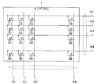
- FIG. 2 is a schematic diagram illustrating a configuration of the touch panel 3 provided in the touch panel system 50.
- the touch panel system 50 includes a touch panel 3 and a capacitance value distribution detection circuit (touch panel controller) 2.
- the touch panel 3 includes signal lines HL1 to HLM (first signal lines) arranged in parallel with each other along the horizontal direction and signal lines VL1 to VLM (second signal lines) arranged in parallel with each other along the vertical direction. And capacitances C11 to CMM formed at the intersections of the signal lines HL1 to HLM and the signal lines VL1 to VLM, respectively.
- the touch panel 3 preferably has a size that allows the user to wear a hand holding the input pen, but may be a size used for a smartphone.
- the capacitance value distribution detection circuit 2 includes a driver 5.
- the driver 5 applies a voltage to the drive lines DL1 to DLM based on the code sequence.
- the capacitance value distribution detection circuit 2 is provided with a sense amplifier 6.
- the sense amplifier 6 reads out a linear sum of charges corresponding to the respective capacitances through the sense lines SL1 to SLM and supplies it to the AD converter 8.
- the capacitance value distribution detection circuit 2 has a multiplexer 4.
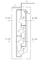
- FIG. 3 shows a connection switching circuit between the signal lines HL1 to HLM and VL1 to VLM connected to the touch panel 3 and the drive lines DL1 to DLM connected to the driver 5 and the sense lines SL1 to SLM connected to the sense amplifier 6. It is a circuit diagram which shows a structure.
- the multiplexer 4 connects the signal lines HL1 to HLM to the drive lines DL1 to DLM of the driver 5, and connects the signal lines VL1 to VLM to the sense lines SL1 to SLM of the sense amplifier 6, and the signal lines HL1 to
- the second connection state in which the HLM is connected to the sense lines SL1 to SLM of the sense amplifier 6 and the signal lines VL1 to VLM are connected to the drive lines DL1 to DLM of the driver 5 is switched.
- FIG. 4 is a circuit diagram showing the configuration of the multiplexer 4 provided in the capacitance distribution detection circuit 2 of the touch panel system 50.
- the multiplexer 4 has four CMOS switches SW1 to SW4 connected in series.
- the control line CL from the timing generator 7 includes a PMOS gate of the CMOS switch SW1, an NMOS gate of the CMOS switch SW2, a PMOS gate of the CMOS switch SW3, an NMOS gate of the CMOS switch SW4, and an inverter inv. Connected to the input.
- the output of the inverter inv is connected to the NMOS gate of the CMOS switch SW1, the PMOS gate of the CMOS switch SW2, the NMOS gate of the CMOS switch SW3, and the PMOS gate of the CMOS switch SW4.
- the signal lines HL1 to HLM are connected to the CMOS switches SW1 and SW2.
- the signal lines VL1 to VLM are connected to the CMOS switches SW3 and SW4.
- the drive lines DL1 to DLM are connected to the CMOS switches SW1 and SW4.
- the sense lines SL1 to SLM are connected to the CMOS switches SW2 and SW3.
- the signal lines HL1 to HLM are connected to the drive lines DL1 to DLM, and the signal lines VL1 to VLM are connected to the sense lines SL1 to SLM.
- the signal lines HL1 to HLM are connected to the sense lines SL1 to SLM, and the signal lines VL1 to VLM are connected to the drive lines DL1 to DLM.
- the AD converter 8 AD converts the linear sum of the charges corresponding to the respective capacitances read through the sense lines SL1 to SLM, and supplies it to the capacitance distribution calculation unit 9.
- the capacitance distribution calculation unit 9 calculates the capacitance distribution on the touch panel 3 based on the linear sum of the charges and the code series corresponding to each capacitance supplied from the AD converter 8 to calculate the touch recognition unit 10. To supply.
- the touch recognition unit 10 recognizes the touched position on the touch panel 3 based on the capacitance distribution supplied from the capacitance distribution calculation unit 9.
- the capacitance value distribution detection circuit 2 has a timing generator 7.
- the timing generator 7 generates a signal that defines the operation of the driver 5, a signal that defines the operation of the sense amplifier 6, and a signal that defines the operation of the AD converter 8, and the driver 5, the sense amplifier 6, and This is supplied to the AD converter 8.
- FIGS. 5A and 5B and FIG. 6 are schematic diagrams for explaining an operation method of the touch panel system 50.
- the phantom noise NZ occurs between the circumscribed lines L1 and L2 circumscribed along the sense lines SL1 to SLM on the hand-held region HDR and outside the hand-held region HDR.
- the pen signal input to the pen input position P existing on the sense line that does not overlap the touched area HDR, that is, outside the circumscribed lines L1 and L2 is the pen input position. Since the phantom noise NZ does not occur on the sense line passing through P, the SNR is not deteriorated by the phantom noise NZ and can be detected.
- phantom noise occurs when the linear signal is read from the horizontal signal line by driving the vertical signal line.
- the drive lines DL1 to DLM and the sense lines SL1 to SLM are interchanged, and the horizontal signal lines HL1 to HLM function as the drive lines DL1 to DLM as shown in FIG. If the signal lines VL1 to VLM are made to function as the sense lines SL1 to SLM to detect signals outside the circumscribed lines L3 and L4, the pen signal to the pen input position P can be detected.
- the signal lines HL1 to HLM are connected to the drive lines DL1 to DLM of the driver 5 and the signal lines VL1 to VLM are connected to the sense lines SL1 to SLM of the sense amplifier 6 ((b in FIG. 5). ))
- the second connection state (FIG. 6) in which the signal lines HL1 to HLM are connected to the sense lines SL1 to SLM of the sense amplifier 6 and the signal lines VL1 to VLM are connected to the drive lines DL1 to DLM of the driver 5.
- the phantom noise NZ is generated at the other timing, the SNR of the pen signal is halved. However, if the first connection state and the second connection state are alternately switched, the phantom noise NZ is generated by the touched area HDR. However, the pen signal can be detected.
- the touch panel system 50 drives the signal lines HL1 to HLM to output the charges corresponding to the capacitance from the signal lines VL1 to VLM at the first time, and the first time after the first time.
- the connection of the signal lines HL1 to HLM and the signal lines VL1 to VLM is controlled by the multiplexer 4, and then at the third time after the second time, the signal lines VL1 to VLM are driven to set the capacitance. Is output from the signal lines HL1 to HLM.
- the capacitance distribution calculation unit 9 is configured not to employ a signal read through a sense line from a capacitance arranged in a rectangle circumscribing the hand-held region HDR.
- the hand region HDR is a region where the hand holding the input conductive pen is put on the touch panel, and can be configured to be recognized by an image recognition unit (not shown). Moreover, you may comprise the area HDR with a handle so that the user of the touchscreen system 1a may define.
- FIG. 7A and 7B are schematic diagrams for explaining another operation method of the touch panel system 50.
- FIG. 7A when the vertical signal lines VL1 to VLM are driven by being connected to the drive lines DL1 to DLM and the horizontal signal lines HL1 to HLM are connected to the sense lines SL1 to SLM, the finger is touched. Phantom noise NZ generated between the circumscribed lines L5 and L6 circumscribing the finger touch area FR along the horizontal direction and outside the finger touch area FR is read through the sense line together with a signal corresponding to the finger touch area FR. Then, as shown in FIG.
- the phantom noise NZ between the circumscribed lines L5 and L6 shown in FIG. 7A and the phantom noise NZ between the circumscribed lines L7 and L8 shown in FIG. 7B are randomly generated regardless of each other. Therefore, the signal corresponding to the phantom noise NZ and the finger touch area FR between the circumscribed lines L5 and L6 read through the sense line shown in FIG. 7A and the sense line shown in FIG.
- the phantom noise NZ between the circumscribed lines L5 and L6 and the phantom between the circumscribed lines L7 and L8 Noise NZ can be canceled.
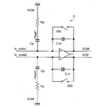
- FIG. 8 is a circuit diagram for explaining a floating node that is capacitively coupled to the first and second signal lines of the touch panel system via a parasitic capacitance.
- the adjacent first signal line or the second signal line of the touch panel 3 is connected to the differential amplifier of the sense amplifier 6 provided in the capacitance value distribution detection circuit 2 via the adjacent sense line.
- a floating node Float1 is electrostatically coupled to one of the adjacent signal lines via a parasitic capacitance Cp.
- the floating node Float1 is DC grounded via a relatively high resistance Rp.
- a floating node Float2 is electrostatically coupled to the other of the adjacent signal lines via a parasitic capacitance Cp.
- the floating node Float2 is DC grounded via a relatively high resistance Rp.
- a switch SW and an integration capacitor Cint are coupled in parallel with each other between the inverting input of the differential amplifier and the corresponding output.
- a switch SW and an integration capacitor Cint are coupled in parallel with each other between the non-inverting input of the differential amplifier and the corresponding output.
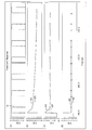
- FIG. 9A is a waveform diagram showing the control signal S1 of the touch panel system
- FIG. 9B is a waveform diagram showing voltage signals S21 and S22 of the floating node
- FIG. It is a wave form diagram which shows voltage signal S31 * S32 of a signal line
- (d) is a wave form diagram which shows the output waveform of the differential amplifier connected to the said 1st, 2nd signal line.
- the first or second signal line is driven as a drive line, and after the time 100 ⁇ sec, the first or second signal line is switched and used as a sense line.
- the voltage signal S31 indicates that the first or second signal line was driven as a drive line at 3.3 V until time 100 ⁇ sec, and after time 100 ⁇ sec, The first or second signal line is used as a sense line, and the corresponding switch SW is closed to converge to the common voltage.
- the common voltage is about half of the power supply voltage, and here is about 1.65V.
- the voltage signal S32 indicates that the adjacent first or second signal line was driven as a drive line at 0 V until time 100 ⁇ sec, and after the time 100 ⁇ sec, the first or second signal line is used as a sense line. The corresponding switch SW is closed and converges to the common voltage.
- the voltage signal S21 of the floating node Float1 increases with a slow time constant as a result of the change of the voltage signal S31. . Then, the voltage signal S22 of the floating node Float2 is attracted by the change of the voltage signal S32 and decreases with a slow time constant.
- the voltage signals S21 and S22 If the value of the resistor Rp is very small, it is immediately grounded to the power supply voltage VCM, so that the voltage signals S21 and S22 immediately converge to the common voltage, but if the value of the resistor Rp is large to some extent, the voltage signals S21 and S22. Changes slowly. Thus, when the floating node is DC-grounded through a relatively high resistance Rp of mega ⁇ and giga ⁇ , the voltage signals S21 and S22 representing noise based on the floating node change with a slow time constant. I will do it.
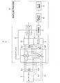
- FIG. 10 is a block diagram showing a configuration of touch panel system 1a according to the first embodiment.
- the same components as those described above are denoted by the same reference numerals, and detailed description thereof will be omitted.
- the touch panel system 1a includes a capacitance value distribution detection device (touch panel controller) 2a.
- the capacitance value distribution detection device 2a is provided with a driver (drive unit) 5a.
- the sense amplifier (amplifier) 6 is composed of a differential amplifier that differentially amplifies the outputs of adjacent signal lines.
- the driver 5a drives the signal lines HL1 to HLM (a plurality of first signal lines) with the same drive value and outputs a first linear sum signal based on the charge of the capacitance to the signal lines VL1 to VLM ( Output from a plurality of second signal lines).
- the sense amplifier 6 amplifies the first linear sum signal output from the signal lines VL1 to VLM at the first time.
- the driver 5a drives the signal lines VL1 to VLM (a plurality of second signal lines) based on the code series at the second time which is the driving timing next to the first time, and charges the electrostatic capacitance.
- the signal lines HL1 to HLM a plurality of first signal lines.
- the sense amplifier 6 amplifies the second linear sum signal output from the signal lines HL1 to HLM (a plurality of first signal lines) at the second time.
- the capacitance distribution calculation unit 9 calculates the distribution of capacitance values based on the second linear sum signal amplified by the sense amplifier 6 and AD-converted by the AD converter 8 and the code sequence.
- the driver 5a drives the signal lines HL1 to HLM immediately before sensing with the same drive value.
- FIG. 11A is a waveform diagram showing the control signal S1 of the touch panel system 1a
- FIG. 11B is a waveform diagram showing the voltage of the floating node of the touch panel system 1a
- FIG. 12 is a waveform diagram showing voltages of signal lines HL1 to HLM of the touch panel system 1a
- FIG. 11D is a waveform diagram showing output waveforms of differential amplifiers connected to the signal lines HL1 to HLM.
- the voltage signal S31 is 3.3V before the time 100 ⁇ sec and the voltage signal S32 is 0V.
- the signal lines HL1 to HLM are set to the same drive value (for example, immediately before the signal line HL1 to HLM). Therefore, as shown in FIG. 11C, the voltage signal S31 and the voltage signal S32 are both 0V before the time 100 ⁇ sec and change in the same waveform after the time 100 ⁇ sec. Since the voltage signal S31 and the voltage signal S32 of the signal line change with the same waveform, the voltage signal S21 and the voltage signal S22 of the floating node also change with the same waveform.
- all the signal lines HL1 to HLM immediately before reading by the sense amplifier 6 are driven with the same drive value, for example, when driving with a code sequence called M series, all signal lines are driven with the same drive value in the M series. Since there is no arrangement of codes to be driven, all signal lines HL1 to HLM are driven with the same drive value by a dummy pattern that is not decoded. For example, all the signal lines HL1 to HLM may be driven at 0V, or all the signal lines HL1 to HLM may be driven at 3.3V. Further, all the signal lines HL1 to HLM may be driven with a common voltage.
- the common voltage is a voltage when the input / output of the differential amplifier is reset, and is generally a half of the power supply voltage.
- FIG. 12 is a block diagram showing a configuration of touch panel system 1b according to the second embodiment.
- the same components as those described above are denoted by the same reference numerals, and detailed description thereof will be omitted.
- the touch panel system 1b includes a capacitance value distribution detection device (touch panel controller) 2b.
- the electrostatic capacitance value distribution detection device 2b is provided with a driver (drive unit) 5b and a capacitance distribution calculation unit 9b.
- the driver 5b drives the signal lines HL1 to HLM (a plurality of first signal lines) based on the code series at the first time, and outputs the first linear sum signal based on the charge of the capacitance to the signal lines VL1 to VLM. (Multiple second signal lines) are output.
- the sense amplifier (amplifier) 6 amplifies the first linear sum signals output from the signal lines VL1 to VLM at the first time.
- the driver 5b drives the signal lines VL1 to VLM based on the code series at the second time, and outputs a second linear sum signal based on the charge of the capacitance from the signal lines HL1 to HLM.
- the sense amplifier 6 amplifies the second linear sum signal output from the signal lines HL1 to HLM at the second time.
- the signal lines VL1 to VLM are capacitively coupled to the floating node through parasitic capacitance.
- the driver 5b drives the signal lines HL1 to HLM so that the sign of the first linear sum signal is inverted in time series. Then, the capacity distribution calculation unit 9b executes subtraction processing at the time of decoding corresponding to the inversion driving.
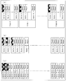
- FIGS. 13A and 13B are diagrams for explaining a method of reversing the electrostatic capacitance by the touch panel system 1b.
- FIG. 13 shows a driving method in which driving in vector units is continued to invert even-numbered driving (the even-numbered driving location to be inverted is shown in white on a black background).
- the inversion drive is performed by the vector drive Vector0 of the frame drive Frame1.
- the inversion drive is performed by the vector drive Vector0 of the frame drive Frame3.
- the inversion is performed in units of two phase driving.
- the period of the same data is a period corresponding to two phase driving.
- the polarity of the even-numbered time-series data of the same data is inverted by inversion driving.
- phase driving Phase 0 included in the vector driving Vector 0 of the frame driving Frame 0 is used for driving.
- inversion driving is performed by phase driving Phase 0 included in vector driving Vector 0 of frame driving Frame 1.
- phase driving Phase 0 included in the vector driving Vector 0 of the frame driving Frame 2 is driven.
- phase drive Phase 0 inversion included in the vector drive Vector 0 of the frame drive Frame 3 is driven.
- Inversion is performed in one phase drive unit.
- the period of the same data is a period corresponding to one phase drive.
- the polarity of the same data is inverted at even times.
- FIG. 14 is a block diagram showing a configuration of touch panel system 1c according to the third embodiment.
- the same components as those described above are denoted by the same reference numerals, and detailed description thereof will be omitted.
- the touch panel system 1c includes a capacitance value distribution detection device (touch panel controller) 2c.
- the capacitance value distribution detection device 2c is provided with a driver (drive unit) 5c, an AD converter 8c, and a capacitance distribution calculation unit 9c.
- the signal lines HL1 to HLM are capacitively coupled to the first floating node via a first parasitic capacitance
- the signal lines VL1 to VLM (a plurality of second signal lines) are connected to the second floating node. It is capacitively coupled to the second floating node via a parasitic capacitance.
- the capacitance value distribution detection device 2c has a calibration mode in which there is no touch input to the capacitance, and a scan mode in which the touch input to the capacitance is detected.
- the driver 5c drives the signal lines HL1 to HLM based on the code series at the first calibration mode time, and outputs the calibration mode first linear sum signal based on the charge of the capacitance from the signal lines VL1 to VLM.
- the signal lines VL1 to VLM are driven based on the code series and the calibration mode second linear sum signal based on the charge of the capacitance is output from the signal lines HL1 to HLM.
- the sense amplifier 6 amplifies the calibration mode first linear sum signal output from the signal lines VL1 to VLM at the first time in the calibration mode, and at the second time in the calibration mode, the signal lines HL1 to HLM.
- the calibration mode second linear sum signal output from is amplified.
- the capacitance distribution calculation unit 9c calculates a calibration mode capacitance value distribution based on the calibration mode first linear sum signal, the calibration mode second linear sum signal, and the code sequence.
- the driver 5c drives the signal lines HL1 to HLM based on the code series to generate the scan mode first linear sum signal based on the electrostatic charge from the signal lines VL1 to VLM.
- the signal lines VL1 to VLM are driven based on the code series to output the scan mode second linear sum signal based on the electrostatic charge from the signal lines HL1 to HLM. .
- the sense amplifier 6 amplifies the scan mode first linear sum signal output from the signal lines VL1 to VLM at the first time in the scan mode, and from the signal lines HL1 to HLM at the second time in the scan mode.
- the output scan mode second linear sum signal is amplified.
- the capacitance value distribution detection device 2c has a switching circuit (not shown) in the previous stage of the sense amplifier 6.
- the input state of each amplifier circuit provided in the sense amplifier 6 is set to an even phase state (phase 0) in which the 2nth sense line and the (2n + 1) th sense line are input, and (2n + 1). Switching is performed between the odd-numbered phase state (phase 1) in which the second sense line and the (2n + 2) th sense line are input.
- the capacitance distribution calculation unit 9c calculates a scan mode capacitance value distribution based on the scan mode first linear sum signal, the scan mode second linear sum signal, and the code sequence, The distribution of the plurality of capacitance values is calculated by subtracting the calibration mode capacitance value distribution from the capacitance value distribution.
- the operation timing of the capacitance value distribution detection device 2c in the calibration mode and the operation timing of the capacitance value distribution detection device 2c in the scan mode are the same.
- the operation timing includes the frame addition number of frame driving based on the code sequence, the driving order based on the code sequence, the first and second linear sum signals in the calibration mode, and the first and second linear sum signals in the scan mode. Includes sampling frequency.
- the capacitance value distribution detection device 2c detects the capacitance, but when it is actually connected to the touch panel 3, the touch panel 3 has manufacturing variations. The output does not become zero, and some output data is output. This operation mode is called a calibration mode, and the output data at this time is called calibration data. An operation mode for detecting touch input is called a scan mode, and output data at this time is called scan data. Then, the calibration data is subtracted from the scan data to obtain a distribution of capacitance values.
- the same operation is repeated many times to obtain a highly accurate signal. For example, when driving in parallel, drive with the first vector of the code sequence, drive with the second vector, and decode by the capacity distribution calculation unit when driving up to the eighth vector in order is completed.
- the capacitance value for one frame can be calculated by calculation.
- the capacitance value for the second frame can be calculated. If such an operation is repeated many times, for example, if it is repeated eight times, capacitance value data for eight frames is calculated. Data obtained by averaging the capacitance value data for the eight frames is calculated and set as a true capacitance value.
- This number of frame repetitions for calculating the true capacitance value is called the frame addition number.
- the noise mixed in based on the floating node is the noise that has the same fixed pattern every time the signal line is driven, so if the frame addition number in the calibration mode is the same as the frame addition number in the scan mode, the scan By subtracting the calibration mode capacitance value distribution from the mode capacitance value distribution, the noise is canceled and disappears.
- FIG. 15 are diagrams for explaining an implementation unit for driving a capacitance by the touch panel system.
- FIG. 15 is a figure for demonstrating the drive of a frame unit.
- the touch panel system 1c repeats (M + 1) frame drive Frame0 to FrameM in this order.
- Each frame drive Frame 0 to Frame M includes (N + 1) vector drives Vector 0 to Vector N, respectively.
- Each of the vector drives Vector0 to VectorN includes an even-numbered phase drive Phase0 and an odd-numbered phase drive Phase1.
- phase 0 In the even phase drive Phase 0 in the even phase state (phase 0), a value corresponding to an even line-odd line (for example, (SL2-SL1), (SL4-SL3), (SL6-SL5)) is output,
- the odd phase drive Phase1 in the odd phase state (phase 1) outputs a value corresponding to an odd line-even line (for example, (SL3-SL2), (SL5-SL4), (SL7-SL6)).
- (B) of FIG. 15 is a figure for demonstrating the drive of a vector unit.
- the vector drive Vector0 of the frame drive Frame0 the vector drive Vector0 of the frame drive Frame1
- the vector drive Vector0 of the frame drive Frame2 the vector drive Vector0 included in each frame drive Frame0 to FrameM in the order of the vector drive Vector0 of the frame drive FrameM. Drives continuously with only Vector0.
- vectors included in each frame drive Frame 0 to Frame M in the order of vector drive Vector 2 of frame drive Frame 0, vector drive Vector 2 of frame drive Frame 1, vector drive Vector 2 of frame drive Frame 2,..., Vector drive Vector 2 of frame drive Frame M It drives continuously only by drive Vector2.
- the driving is performed up to the vector driving VectorN.
- (C) of FIG. 15 is a figure for demonstrating the drive of a phase unit.
- the phase drive Phase0 included in the vector drive Vector0 of the frame drive Frame0 the phase drive Phase0 included in the vector drive Vector0 of the frame drive Frame1
- the phase drive Phase0 included in the vector drive Vector0 of the frame drive Frame2 the frame drive FrameM
- the driving is continuously performed only by the phase driving Phase 0 of the vector driving Vector 0 included in each frame driving Frame 0 to Frame M in the order of the phase driving Phase 0 included in the vector driving Vector 0.
- phase drive Phase 1 included in the vector drive Vector 0 of the frame drive Frame 0 the phase drive Phase 1 included in the vector drive Vector 0 of the frame drive Frame 1
- phase drive Phase 1 included in the vector drive Vector 0 of the frame drive Frame 2 the phase drive Phase 1 included in the vector drive Vector 0 of the frame drive Frame 2
- the drive is continuously performed only by the phase drive Phase 1 of the vector drive Vector 0 included in each frame drive Frame 0 to Frame M.
- the phase drive Phase0 included in the vector drive Vector1 of the frame drive Frame0 the phase drive Phase0 included in the vector drive Vector1 of the frame drive Frame1
- the phase drive Phase0 included in the vector drive Vector1 of the frame drive Frame2 the phase drive Phase0 included in the vector drive Vector1 of the frame drive Frame2
- the frame drive FrameM the frame drive FrameM
- the drive is continuously performed only by the phase drive Phase 0 of the vector drive Vector 1 included in each frame drive Frame 0 to Frame M. Thereafter, similarly, the driving is performed up to the vector driving VectorN.
- the calibration mode capacitance value distribution is subtracted from the scan mode capacitance value distribution. Noise is canceled and disappears.
- the calibration mode static value distribution is determined from the scan mode capacitance value distribution. By subtracting the capacitance value distribution, the noise is canceled and disappears.
- the calibration mode if the driving is performed in the phase unit driving order shown in FIG. 15C, and the scanning mode is also driven in the phase unit driving order, the calibration mode is calculated from the scan mode capacitance value distribution. By subtracting the capacitance value distribution, the noise is canceled and disappears.
- FIG. 16 is a block diagram showing a configuration of a touch panel system 1d according to the fourth embodiment.
- the same components as those described above are denoted by the same reference numerals, and detailed description thereof will be omitted.
- the touch panel system 1d includes a capacitance value distribution detection device (touch panel controller) 2d.
- the capacitance value distribution detection device 2d is provided with a driver (driving unit) 5d.
- the driver 5d drives the signal lines HL1 to HLM (a plurality of first signal lines) based on the code series at the first time, and outputs the first linear sum signal based on the charge of the capacitance to the signal lines VL1 to VLM. (Multiple second signal lines) are output.
- the sense amplifier 6 amplifies the first linear sum signal output from the signal lines VL1 to VLM at the first time.
- the driver 5d drives the signal lines VL1 to VLM based on the code series to output the second linear sum signal based on the charge of the capacitance from the signal lines HL1 to HLM.
- the sense amplifier 6 amplifies the second linear sum signal output from the signal lines HL1 to HLM at the second time. This second time is a time after the connection of the signal lines HL1 to HLM is switched from the driver 5b to the sense amplifier 6 and the voltage of the floating node capacitively coupled to the signal lines HL1 to HLM is stabilized via the parasitic capacitance. .
- the sense amplifier (amplifier) 6 shows the example comprised by the differential amplifier which carries out differential amplification of the output of an adjacent signal line, this invention is not limited to this.
- the sense amplifier 6 may be constituted by a single amplifier instead of the differential amplifier.
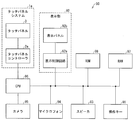
- FIG. 17 is a block diagram showing a configuration of an electronic apparatus (mobile phone 90) according to the fifth embodiment.
- the cellular phone 90 includes a CPU 96, a RAM 97, a ROM 98, a camera 95, a microphone 94, a speaker 93, an operation key 91, a display unit 92 including a display panel 92b and a display control circuit 92a, and a touch panel system 1a. It has. Each component is connected to each other by a data bus.
- the CPU 96 controls the operation of the mobile phone 90.
- the CPU 96 executes a program stored in the ROM 98, for example.
- the operation key 91 receives an instruction input by the user of the mobile phone 90.
- the RAM 97 volatilely stores data generated by executing a program by the CPU 96 or data input via the operation keys 91.
- the ROM 98 stores data in a nonvolatile manner.
- the ROM 98 is a ROM capable of writing and erasing, such as EPROM (Erasable Programmable Read-Only Memory) and flash memory.
- EPROM Erasable Programmable Read-Only Memory
- flash memory such as EPROM (Erasable Programmable Read-Only Memory) and flash memory.
- the mobile phone 90 may be configured to include an interface (IF) for connecting to another electronic device by wire.
- IF interface
- the camera 95 shoots a subject in accordance with the operation of the operation key 91 by the user.
- the image data of the photographed subject is stored in the RAM 97 or an external memory (for example, a memory card).
- the microphone 94 receives user's voice input.
- the mobile phone 90 digitizes the input voice (analog data). Then, the mobile phone 90 sends the digitized voice to a communication partner (for example, another mobile phone).
- the speaker 93 outputs sound based on, for example, music data stored in the RAM 97.
- the touch panel system 1a includes a touch panel 3 and a touch panel controller 2a.
- the CPU 96 controls the operation of the touch panel system 1a.
- the CPU 96 executes a program stored in the ROM 98, for example.
- the RAM 97 stores data generated by executing the program by the CPU 96 in a volatile manner.
- the ROM 97 stores data in a nonvolatile manner.
- the display panel 92b displays images stored in the ROM 98 and RAM 97 by the display control circuit 92a.
- the display panel 92b is superimposed on the touch panel 3 or contains the touch panel 3 therein.
- the touch panel controller (capacitance value distribution detection circuit 2a) according to the first aspect of the present invention includes a plurality of first signal lines (signal lines HL1 to HLM) and a plurality of second signal lines (signal lines VL1 to VLM).
- a touch panel controller that calculates a distribution of a plurality of capacitance values respectively formed at intersections, wherein the first signal line is capacitively coupled to a first floating node via a first parasitic capacitance, The second signal line is capacitively coupled to the second floating node via the second parasitic capacitance, and at the first time, the plurality of first signal lines are driven with the same driving value to charge the electrostatic capacitance.
- a driver for outputting a first linear sum signal based on the second signal line from the second signal line
- an amplifier for amplifying the first linear sum signal output from the second signal line at the first time. 6
- the driving unit drives the second signal line based on a code series at a second time which is a driving timing next to the first time, and is based on the charge of the capacitance.
- the second linear sum signal is output from the first signal line, the amplifier amplifies the second linear sum signal output from the first signal line at the second time, and the amplifier A differential amplifier corresponding to one signal line and an adjacent second signal line, and a capacitance distribution calculation unit that calculates a distribution of the capacitance value based on the second linear sum signal and the code sequence; It has more.
- the linear sum signal is output from the first signal line at the drive timing immediately after driving the plurality of first signal lines with the same drive value, and the capacitance value is based on the linear sum signal.
- the capacitance value is based on the linear sum signal.
- the touch panel controller (capacitance value distribution detection circuit 2b) according to aspect 2 of the present invention has a plurality of capacitance values respectively formed at intersections of the plurality of first signal lines and the plurality of second signal lines.
- a touch panel controller for calculating a distribution, wherein, at a first time, the first signal line is driven based on a code series, and a first linear sum signal based on the charge of the capacitance is output from the second signal line And a driver for amplifying the first linear sum signal output from the second signal line at the first time, and the drive unit at the second time
- a signal line is driven based on the code series to output a second linear sum signal based on the charge of the capacitance from the first signal line, and the amplifier is configured to output the first signal line at the second time.
- the second linear sum signal is amplified, the second signal line is capacitively coupled to the floating node through a parasitic capacitance, and the driving unit determines whether the sign of the first linear sum signal is in time series.
- the first signal line is driven so as to be inverted.
- the driving unit drives the first signal line so that the sign of the first linear sum signal is inverted in time series, so that low frequency noise can be reduced. it can. Since the noise based on the floating node is low-frequency noise, the noise based on the floating node can be reduced by driving with the sign reversed.
- the touch panel controller (capacitance value distribution detection circuit 2c) according to the aspect 3 of the present invention has a plurality of capacitance values respectively formed at intersections of the plurality of first signal lines and the plurality of second signal lines.
- a touch panel controller for calculating a distribution wherein the first signal line is capacitively coupled to a first floating node via a first parasitic capacitor, and the second signal line is coupled to a first parasitic capacitor via a second parasitic capacitor.
- the touch panel controller has a calibration mode in which there is no touch input to the capacitance, and a scan mode in which the touch input to the capacitance is detected.
- the first signal line is driven based on the code series, and the calibration mode first line is based on the charge of the capacitance.
- a sum signal is output from the second signal line, and at the second calibration mode time, the second signal line is driven based on the code series and the calibration mode second linear based on the charge of the capacitance.
- a drive unit (driver 5c) for outputting a sum signal from the first signal line, and amplifying the calibration mode first linear sum signal outputted from the second signal line at the first time in the calibration mode; An amplifier that amplifies the calibration mode second linear sum signal output from the first signal line at the second time in the calibration mode; the calibration mode first linear sum signal; and the calibration mode second linear sum.
- a calibration mode capacitance value based on the signal and the code sequence A capacitance distribution calculation unit that calculates a first scan mode based on the charge of the capacitance by driving the first signal line based on the code sequence at a first scan mode time.
- a linear sum signal is output from the second signal line, and at the second time in the scan mode, the second signal line is driven based on the code series, and the scan mode second linear sum is based on the charge of the capacitance.
- a signal is output from the first signal line, and the amplifier amplifies the scan mode first linear sum signal output from the second signal line at the first time in the scan mode and the second time in the scan mode.
- a scan mode capacitance value distribution is calculated based on the scan mode second linear sum signal and the code sequence, and the calibration mode capacitance value distribution is subtracted from the scan mode capacitance value distribution.
- the distribution of the plurality of capacitance values is calculated, and the operation timing in the calibration mode and the operation timing in the scan mode are made the same.
- noise of the same pattern is mixed from the first floating node and the second floating node every time. Therefore, if the operation timing in the calibration mode and the operation timing in the scan mode are the same, By subtracting the calibration mode capacitance value distribution from the scan mode capacitance value distribution, the noise mixed in the calibration mode and the noise mixed in the scan mode can be canceled and eliminated.
- the touch panel controller according to aspect 4 of the present invention is the touch panel controller according to aspect 3, in which the operation timing includes the number of frame additions based on the code sequence, the drive order based on the code sequence, and the first and second calibration modes.
- the sampling frequency of the linear sum signal and the scan mode first and second linear sum signals may be included.
- the calibration mode capacitance value distribution can be changed from the scan mode capacitance value distribution.
- the noise mixed in the calibration mode and the noise mixed in the scan mode can be canceled and eliminated.
- the touch panel controller (capacitance value distribution detection circuit 2d) according to the fifth aspect of the present invention has a plurality of capacitance values respectively formed at intersections of the plurality of first signal lines and the plurality of second signal lines.
- a touch panel controller for calculating a distribution, wherein, at a first time, the first signal line is driven based on a code series, and a first linear sum signal based on the charge of the capacitance is output from the second signal line
- a driver for amplifying the first linear sum signal output from the second signal line at the first time, and the drive unit performs the second operation at the second time.
- a signal line is driven based on the code series to output a second linear sum signal based on the charge of the capacitance from the first signal line, and the amplifier is configured to output the first signal line at the second time. Is output from Amplifying the second linear sum signal, the second time, the voltage of the floating node capacitively coupled to said first signal line via the parasitic capacitance is time after the stable.
- the second signal line is driven based on the code sequence at the second time after the voltage of the floating node capacitively coupled to the first signal line is stabilized via the parasitic capacitance. Since the second linear sum signal based on the electric charge of the capacitance is output from the first signal line, the second signal is reduced after noise based on the floating node capacitively coupled to the first signal line via the parasitic capacitance is reduced. Drive the line. For this reason, the influence of the noise on the driving of the second signal line can be reduced.
- the amplifier is a differential amplifier corresponding to the adjacent first signal line and the adjacent second signal line. preferable.
- the noise immunity can be further increased by the differential amplification configuration.
- a touch panel system according to aspect 7 of the present invention includes the touch panel controller according to any one of aspects 1 to 3 and 5.
- An electronic device (mobile phone 90) according to aspect 8 of the present invention includes the touch panel system according to aspect 7 described above.
- the present invention relates to a touch panel controller that calculates a distribution of a plurality of capacitance values respectively formed at intersections of a plurality of first signal lines and a plurality of second signal lines, and a touch panel system and electronic apparatus using the same. Can be used.
- Capacitance value distribution detection circuit touch panel controller
- 5a to 5d driver sense amplifier (amplifier)
- 9c, 9d Capacity distribution calculation unit 90 Mobile phone (electronic device) HL1 to HLM signal line (first signal line) VL1 to VLM signal lines (second signal lines) Cp parasitic capacitance (first parasitic capacitance, second parasitic capacitance) Float1, Float2 floating nodes (first floating node, second floating node)
Landscapes
- Engineering & Computer Science (AREA)
- General Engineering & Computer Science (AREA)
- Theoretical Computer Science (AREA)
- Human Computer Interaction (AREA)
- Physics & Mathematics (AREA)
- General Physics & Mathematics (AREA)
- Computer Networks & Wireless Communication (AREA)
- Position Input By Displaying (AREA)
Abstract
Description
本発明者らは、ドライブラインを並列駆動するタッチパネルシステムにおいて、電磁ノイズを受けた人体の手、指等のパネルへのタッチに起因して生じるノイズの影響を除去するために、複数の静電容量がその交点に形成される複数の第1信号線と複数の第2信号線とを交互に駆動する構成を提案している(特願2011-142164号、平成23年6月27日出願)。
図1は、本発明の前提となるタッチパネルシステム50の構成を示すブロック図である。図2は、タッチパネルシステム50に設けられたタッチパネル3の構成を示す模式図である。
図5の(a)(b)、図6は、タッチパネルシステム50の動作方法を説明するための模式図である。図6に示すように、ファントムノイズNZが、お手付き領域HDRにセンスラインSL1~SLMに沿って外接する外接ラインL1・L2の間であって、お手付き領域HDRの外側に発生するという問題がある。しかしながら、図5の(a)に示すように、お手付き領域HDRと重ならないセンスライン上、即ち、外接ラインL1・L2の外側に存在するペン入力位置Pに入力されたペン信号は、ペン入力位置Pを通るセンスライン上にファントムノイズNZが発生しないので、ファントムノイズNZによるSNRの劣化が無く、検出可能である。
図8は、上記タッチパネルシステムの第1及び第2信号線に寄生容量を介して容量結合するフローティングノードを説明するための回路図である。
以下、本発明の実施の形態について、詳細に説明する。
図10は、実施の形態1に係るタッチパネルシステム1aの構成を示すブロック図である。前述した構成要素と同一の構成要素には同一の参照符号を付し、それらの詳細な説明は省略する。
図11の(a)はタッチパネルシステム1aの制御信号S1を示す波形図であり、図11の(b)はタッチパネルシステム1aのフローティングノードの電圧を示す波形図であり、図11の(c)はタッチパネルシステム1aの信号線HL1~HLMの電圧を示す波形図であり、図11の(d)は信号線HL1~HLMに接続された差動増幅器の出力波形を示す波形図である。
(タッチパネルシステム1bの構成)
図12は、実施の形態2に係るタッチパネルシステム1bの構成を示すブロック図である。前述した構成要素と同一の構成要素には同一の参照符号を付し、それらの詳細な説明は省略する。
図13の(a)(b)は、タッチパネルシステム1bにより静電容量を反転駆動する方法を説明するための図である。
(タッチパネルシステム1cの構成)
図14は、実施の形態3に係るタッチパネルシステム1cの構成を示すブロック図である。前述した構成要素と同一の構成要素には同一の参照符号を付し、それらの詳細な説明は省略する。
静電容量値分布検出装置2cは静電容量を検出するが、実際にタッチパネル3に接続したときは、タッチパネル3に製造バラつきがあるので、タッチパネル3にタッチ入力が無いときも、タッチパネル3からの出力は零にならず、何らかの出力データが出力される。この動作モードをキャリブレーションモードと呼び、このときの出力データをキャリブレーションデータという。また、タッチ入力を検出する動作モードをスキャンモードと呼び、このときの出力データをスキャンデータという。そして、スキャンデータからキャリブレーションデータを減算して静電容量の値の分布を求める。
(タッチパネルシステム1dの構成)
図16は、実施の形態4に係るタッチパネルシステム1dの構成を示すブロック図である。前述した構成要素と同一の構成要素には同一の参照符号を付し、それらの詳細な説明は省略する。
図8及び図9で前述したように、信号線のモードをドライブモードからセンスモードへ反転した後は、フローティングノードの電圧信号S21・S22がゆっくり変化するので、この電圧信号S21・S22が安定するまで、ドライバ5bによる次のタイミングの駆動を待ち、電圧信号S21・S22が安定するまでは、フローティングノードに基づくノイズが入るので、ドライバ5bはドライブラインを介して信号線VL1~VLMを駆動しない。この構成により、フローティングノードに基づくノイズを低減することができる。
(携帯電話90の構成)
図17は、実施の形態5に係る電子機器(携帯電話90)の構成を示すブロック図である。携帯電話機90は、CPU96と、RAM97と、ROM98と、カメラ95と、マイクロフォン94と、スピーカ93と、操作キー91と、表示パネル92b及び表示制御回路92aを含む表示部92と、タッチパネルシステム1aとを備えている。各構成要素は、相互にデータバスによって接続されている。
本発明の態様1に係るタッチパネルコントローラ(静電容量値分布検出回路2a)は、複数の第1信号線(信号線HL1~HLM)と複数の第2信号線(信号線VL1~VLM)との交点にそれぞれ形成される複数の静電容量の値の分布を算出するタッチパネルコントローラであって、前記第1信号線は、第1寄生容量を介して第1フローティングノードと容量結合しており、前記第2信号線は、第2寄生容量を介して第2フローティングノードと容量結合しており、第1時刻において、前記複数の第1信号線を同じ駆動値で駆動して前記静電容量の電荷に基づく第1線形和信号を前記第2信号線から出力させる駆動部(ドライバ5a)と、前記第1時刻において、前記第2信号線から出力された第1線形和信号を増幅する増幅器(センスアンプ6)とを備え、前記駆動部は、前記第1時刻の次の駆動タイミングである第2時刻において、前記第2信号線を符号系列に基づいて駆動して前記静電容量の電荷に基づく第2線形和信号を前記第1信号線から出力させ、前記増幅器は、前記第2時刻において、前記第1信号線から出力された第2線形和信号を増幅し、前記増幅器は、隣接する第1信号線及び隣接する第2信号線に対応する差動増幅器であり、前記第2線形和信号と前記符号系列とに基づいて前記静電容量の値の分布を計算する容量分布計算部とをさらに備えている。
2a~2d 静電容量値分布検出回路(タッチパネルコントローラ)
5a~5d ドライバ
6 センスアンプ(増幅器)
9、9c、9d 容量分布計算部
90 携帯電話(電子機器)
HL1~HLM 信号線(第1信号線)
VL1~VLM 信号線(第2信号線)
Cp 寄生容量(第1寄生容量、第2寄生容量)
Float1、Float2 フローティングノード(第1フローティングノード、第2フローティングノード)
Claims (6)
- 複数の第1信号線と複数の第2信号線との交点にそれぞれ形成される複数の静電容量の値の分布を算出するタッチパネルコントローラであって、
前記第1信号線は、第1寄生容量を介して第1フローティングノードと容量結合しており、前記第2信号線は、第2寄生容量を介して第2フローティングノードと容量結合しており、
第1時刻において、前記複数の第1信号線を同じ駆動値で駆動して前記静電容量の電荷に基づく第1線形和信号を前記第2信号線から出力させる駆動部と、
前記第1時刻において、前記第2信号線から出力された第1線形和信号を増幅する増幅器とを備え、
前記駆動部は、前記第1時刻の次の駆動タイミングである第2時刻において、前記第2信号線を符号系列に基づいて駆動して前記静電容量の電荷に基づく第2線形和信号を前記第1信号線から出力させ、
前記増幅器は、前記第2時刻において、前記第1信号線から出力された第2線形和信号を増幅し、
前記増幅器は、隣接する第1信号線及び隣接する第2信号線に対応する差動増幅器であり、
前記第2線形和信号と前記符号系列とに基づいて前記静電容量の値の分布を計算する容量分布計算部とをさらに備えることを特徴とするタッチパネルコントローラ。 - 複数の第1信号線と複数の第2信号線との交点にそれぞれ形成される複数の静電容量の値の分布を算出するタッチパネルコントローラであって、
第1時刻において、前記第1信号線を符号系列に基づいて駆動して前記静電容量の電荷に基づく第1線形和信号を前記第2信号線から出力させる駆動部と、
前記第1時刻において、前記第2信号線から出力された第1線形和信号を増幅する増幅器とを備え、
前記駆動部は、第2時刻において、前記第2信号線を前記符号系列に基づいて駆動して前記静電容量の電荷に基づく第2線形和信号を前記第1信号線から出力させ、
前記増幅器は、前記第2時刻において、前記第1信号線から出力された第2線形和信号を増幅し、
前記第2信号線は、寄生容量を介してフローティングノードと容量結合しており、
前記駆動部は、前記第1線形和信号の符号の正負が時系列に沿って反転するように前記第1信号線を駆動することを特徴とするタッチパネルコントローラ。 - 複数の第1信号線と複数の第2信号線との交点にそれぞれ形成される複数の静電容量の値の分布を算出するタッチパネルコントローラであって、
前記第1信号線は、第1寄生容量を介して第1フローティングノードと容量結合しており、前記第2信号線は、第2寄生容量を介して第2フローティングノードと容量結合しており、
前記タッチパネルコントローラは、前記静電容量へのタッチ入力が無いキャリブレーションモードと、前記静電容量へのタッチ入力を検出するスキャンモードとを有し、
キャリブレーションモード第1時刻において、前記第1信号線を符号系列に基づいて駆動して前記静電容量の電荷に基づくキャリブレーションモード第1線形和信号を前記第2信号線から出力させると共に、キャリブレーションモード第2時刻において、前記第2信号線を前記符号系列に基づいて駆動して前記静電容量の電荷に基づくキャリブレーションモード第2線形和信号を前記第1信号線から出力させる駆動部と、
前記キャリブレーションモード第1時刻において、前記第2信号線から出力されたキャリブレーションモード第1線形和信号を増幅すると共に、前記キャリブレーションモード第2時刻において、前記第1信号線から出力されたキャリブレーションモード第2線形和信号を増幅する増幅器と、
前記キャリブレーションモード第1線形和信号と前記キャリブレーションモード第2線形和信号と前記符号系列とに基づいて、キャリブレーションモード静電容量値分布を計算する容量分布計算部とを備え、
前記駆動部は、スキャンモード第1時刻において、前記第1信号線を前記符号系列に基づいて駆動して前記静電容量の電荷に基づくスキャンモード第1線形和信号を前記第2信号線から出力させると共に、スキャンモード第2時刻において、前記第2信号線を前記符号系列に基づいて駆動して前記静電容量の電荷に基づくスキャンモード第2線形和信号を前記第1信号線から出力させ、
前記増幅器は、前記スキャンモード第1時刻において、前記第2信号線から出力されたスキャンモード第1線形和信号を増幅するとともに、前記スキャンモード第2時刻において、前記第1信号線から出力されたスキャンモード第2線形和信号を増幅し、
前記容量分布計算部は、前記スキャンモード第1線形和信号と前記スキャンモード第2線形和信号と前記符号系列とに基づいて、スキャンモード静電容量値分布を計算し、前記スキャンモード静電容量値分布から前記キャリブレーションモード静電容量値分布を減算することにより前記複数の静電容量の値の分布を算出し、
前記キャリブレーションモードにおける動作タイミングと、前記スキャンモードにおける動作タイミングとを同じにしたことを特徴とするタッチパネルコントローラ。 - 複数の第1信号線と複数の第2信号線との交点にそれぞれ形成される複数の静電容量の値の分布を算出するタッチパネルコントローラであって、
第1時刻において、前記第1信号線を符号系列に基づいて駆動して前記静電容量の電荷に基づく第1線形和信号を前記第2信号線から出力させる駆動部と、
前記第1時刻において、前記第2信号線から出力された第1線形和信号を増幅する増幅器とを備え、
前記駆動部は、第2時刻において、前記第2信号線を前記符号系列に基づいて駆動して前記静電容量の電荷に基づく第2線形和信号を前記第1信号線から出力させ、
前記増幅器は、前記第2時刻において、前記第1信号線から出力された第2線形和信号を増幅し、
前記第2時刻は、寄生容量を介して前記第1信号線と容量結合するフローティングノードの電圧が安定した後の時刻であることを特徴とするタッチパネルコントローラ。 - 前記増幅器は、隣接する第1信号線及び隣接する第2信号線に対応する差動増幅器である請求項2~4のいずれかに記載のタッチパネルコントローラ。
- 請求項1~4のいずれかに記載のタッチパネルコントローラを有するタッチパネルシステムを備えたことを特徴とする電子機器。
Priority Applications (3)
| Application Number | Priority Date | Filing Date | Title |
|---|---|---|---|
| JP2014550137A JP5792399B2 (ja) | 2012-11-30 | 2013-11-19 | タッチパネルコントローラ、並びにこれを用いた電子機器 |
| CN201380061874.1A CN104813262B (zh) | 2012-11-30 | 2013-11-19 | 触摸面板控制器和使用其的电子设备 |
| US14/646,446 US20150338955A1 (en) | 2012-11-30 | 2013-11-19 | Touch panel controller and electronic device using same |
Applications Claiming Priority (2)
| Application Number | Priority Date | Filing Date | Title |
|---|---|---|---|
| JP2012263806 | 2012-11-30 | ||
| JP2012-263806 | 2012-11-30 |
Publications (1)
| Publication Number | Publication Date |
|---|---|
| WO2014084089A1 true WO2014084089A1 (ja) | 2014-06-05 |
Family
ID=50827732
Family Applications (1)
| Application Number | Title | Priority Date | Filing Date |
|---|---|---|---|
| PCT/JP2013/081159 Ceased WO2014084089A1 (ja) | 2012-11-30 | 2013-11-19 | タッチパネルコントローラ、並びにこれを用いた電子機器 |
Country Status (4)
| Country | Link |
|---|---|
| US (1) | US20150338955A1 (ja) |
| JP (1) | JP5792399B2 (ja) |
| CN (1) | CN104813262B (ja) |
| WO (1) | WO2014084089A1 (ja) |
Cited By (2)
| Publication number | Priority date | Publication date | Assignee | Title |
|---|---|---|---|---|
| US10415107B2 (en) | 2014-03-04 | 2019-09-17 | Wadeco Co., Ltd. | Method for loading and depositing loaded material in blast furnace, loaded material surface detection device, and method for operating blast furnace |
| JP2022172340A (ja) * | 2019-11-27 | 2022-11-15 | 株式会社 ハイディープ | タッチ入力装置 |
Families Citing this family (5)
| Publication number | Priority date | Publication date | Assignee | Title |
|---|---|---|---|---|
| JP5973072B2 (ja) * | 2013-06-20 | 2016-08-23 | シャープ株式会社 | タッチパネルコントローラ、集積回路、タッチパネル装置、および電子機器 |
| KR102249651B1 (ko) * | 2014-07-23 | 2021-05-10 | 주식회사 실리콘웍스 | 터치패널 센싱 장치 및 그 제어 장치 |
| US10303318B2 (en) * | 2015-10-01 | 2019-05-28 | Sharp Kabushiki Kaisha | Capacitance detection method, position detection method, touch panel controller, and electronic device |
| US10120509B2 (en) * | 2015-12-29 | 2018-11-06 | Stmicroelectronics Asia Pacific Pte Ltd | Common mode noise reduction in capacitive touch sensing |
| KR20170111805A (ko) * | 2016-03-29 | 2017-10-12 | 삼성전자주식회사 | 지문 센서의 단위 픽셀, 및 이를 포함하는 지문 센서 |
Citations (10)
| Publication number | Priority date | Publication date | Assignee | Title |
|---|---|---|---|---|
| JPH09222947A (ja) * | 1996-02-16 | 1997-08-26 | Sharp Corp | 座標入力装置 |
| WO2009107415A1 (ja) * | 2008-02-27 | 2009-09-03 | セイコーインスツル株式会社 | 近接検出装置と近接検出方法 |
| US20090315858A1 (en) * | 2008-06-19 | 2009-12-24 | Hitachi Displays, Ltd. | Display Device with Touch Panel |
| EP2336853A2 (en) * | 2009-12-18 | 2011-06-22 | Wacom Co., Ltd. | Pointer detection apparatus and pointer detection method |
| WO2011114900A1 (ja) * | 2010-03-17 | 2011-09-22 | シャープ株式会社 | タッチセンサ付き表示装置 |
| TW201227456A (en) * | 2010-12-28 | 2012-07-01 | Sharp Kk | Touch panel system and electronic device |
| WO2012141112A1 (ja) * | 2011-04-15 | 2012-10-18 | シャープ株式会社 | 表示装置、表示装置の駆動方法及び電子機器 |
| WO2012176638A1 (en) * | 2011-06-22 | 2012-12-27 | Sharp Kabushiki Kaisha | Touch panel system and electronic device |
| TW201301111A (zh) * | 2011-06-27 | 2013-01-01 | Sharp Kk | 電容量分佈檢測方法、電容量分佈檢測電路、觸碰感測器系統及資訊輸入輸出元件 |
| WO2013061550A1 (en) * | 2011-10-25 | 2013-05-02 | Sharp Kabushiki Kaisha | Touch panel system and electronic device |
Family Cites Families (6)
| Publication number | Priority date | Publication date | Assignee | Title |
|---|---|---|---|---|
| JP2010282539A (ja) * | 2009-06-08 | 2010-12-16 | Sanyo Electric Co Ltd | 静電容量型タッチセンサ用の信号処理回路 |
| TWI443554B (zh) * | 2009-08-05 | 2014-07-01 | Silicon Integrated Sys Corp | 觸碰感測裝置及其方法 |
| TWI438413B (zh) * | 2009-10-09 | 2014-05-21 | Egalax Empia Technology Inc | 訊號量測的方法與裝置 |
| TW201118387A (en) * | 2009-11-19 | 2011-06-01 | Raydium Semiconductor Corp | Capacitance measurement circuit and method therefor |
| JP4927216B1 (ja) * | 2010-11-12 | 2012-05-09 | シャープ株式会社 | 線形素子列値推定方法、静電容量検出方法、集積回路、タッチセンサシステム、及び電子機器 |
| TWI455434B (zh) * | 2012-05-08 | 2014-10-01 | Ind Tech Res Inst | 靜電放電保護裝置及其方法 |
-
2013
- 2013-11-19 CN CN201380061874.1A patent/CN104813262B/zh active Active
- 2013-11-19 US US14/646,446 patent/US20150338955A1/en not_active Abandoned
- 2013-11-19 WO PCT/JP2013/081159 patent/WO2014084089A1/ja not_active Ceased
- 2013-11-19 JP JP2014550137A patent/JP5792399B2/ja active Active
Patent Citations (23)
| Publication number | Priority date | Publication date | Assignee | Title |
|---|---|---|---|---|
| JPH09222947A (ja) * | 1996-02-16 | 1997-08-26 | Sharp Corp | 座標入力装置 |
| US5905489A (en) * | 1996-02-16 | 1999-05-18 | Sharp Kabushiki Kaisha | Coordinate input device |
| WO2009107415A1 (ja) * | 2008-02-27 | 2009-09-03 | セイコーインスツル株式会社 | 近接検出装置と近接検出方法 |
| TW200947268A (en) * | 2008-02-27 | 2009-11-16 | Seiko Instr Inc | Proximity detector and proximity detection method |
| US20110043478A1 (en) * | 2008-02-27 | 2011-02-24 | Kenichi Matsushima | Proximity detection device and proximity detection method |
| US20090315858A1 (en) * | 2008-06-19 | 2009-12-24 | Hitachi Displays, Ltd. | Display Device with Touch Panel |
| JP2010003048A (ja) * | 2008-06-19 | 2010-01-07 | Hitachi Displays Ltd | タッチパネル付き表示装置 |
| EP2336853A2 (en) * | 2009-12-18 | 2011-06-22 | Wacom Co., Ltd. | Pointer detection apparatus and pointer detection method |
| US20110148785A1 (en) * | 2009-12-18 | 2011-06-23 | Wacom Co., Ltd. | Pointer detection apparatus and pointer detection method |
| JP2011128982A (ja) * | 2009-12-18 | 2011-06-30 | Wacom Co Ltd | 指示体検出装置及び指示体検出方法 |
| WO2011114900A1 (ja) * | 2010-03-17 | 2011-09-22 | シャープ株式会社 | タッチセンサ付き表示装置 |
| US20130027338A1 (en) * | 2010-03-17 | 2013-01-31 | Sharp Kabushiki Kaisha | Touch sensor-equipped display device |
| TW201227456A (en) * | 2010-12-28 | 2012-07-01 | Sharp Kk | Touch panel system and electronic device |
| WO2012090537A1 (en) * | 2010-12-28 | 2012-07-05 | Sharp Kabushiki Kaisha | Touch panel system and electronic device |
| JP2012168919A (ja) * | 2010-12-28 | 2012-09-06 | Sharp Corp | タッチパネルシステムおよび電子機器 |
| WO2012141112A1 (ja) * | 2011-04-15 | 2012-10-18 | シャープ株式会社 | 表示装置、表示装置の駆動方法及び電子機器 |
| TW201246148A (en) * | 2011-04-15 | 2012-11-16 | Sharp Kk | Display device, display device driving method, and electronic device |
| KR20130079623A (ko) * | 2011-04-15 | 2013-07-10 | 샤프 가부시키가이샤 | 표시 장치, 표시 장치의 구동 방법 및 전자 기기 |
| WO2012176638A1 (en) * | 2011-06-22 | 2012-12-27 | Sharp Kabushiki Kaisha | Touch panel system and electronic device |
| TW201301111A (zh) * | 2011-06-27 | 2013-01-01 | Sharp Kk | 電容量分佈檢測方法、電容量分佈檢測電路、觸碰感測器系統及資訊輸入輸出元件 |
| JP2013008318A (ja) * | 2011-06-27 | 2013-01-10 | Sharp Corp | 静電容量値分布検出方法、静電容量値分布検出回路、タッチセンサシステム、及び情報入出力機器 |
| WO2013061550A1 (en) * | 2011-10-25 | 2013-05-02 | Sharp Kabushiki Kaisha | Touch panel system and electronic device |
| JP2013092872A (ja) * | 2011-10-25 | 2013-05-16 | Sharp Corp | タッチパネルシステムおよび電子機器 |
Cited By (3)
| Publication number | Priority date | Publication date | Assignee | Title |
|---|---|---|---|---|
| US10415107B2 (en) | 2014-03-04 | 2019-09-17 | Wadeco Co., Ltd. | Method for loading and depositing loaded material in blast furnace, loaded material surface detection device, and method for operating blast furnace |
| JP2022172340A (ja) * | 2019-11-27 | 2022-11-15 | 株式会社 ハイディープ | タッチ入力装置 |
| JP7627954B2 (ja) | 2019-11-27 | 2025-02-07 | 株式会社 ハイディープ | タッチ入力装置 |
Also Published As
| Publication number | Publication date |
|---|---|
| US20150338955A1 (en) | 2015-11-26 |
| CN104813262A (zh) | 2015-07-29 |
| CN104813262B (zh) | 2016-05-18 |
| JPWO2014084089A1 (ja) | 2017-01-05 |
| JP5792399B2 (ja) | 2015-10-14 |
Similar Documents
| Publication | Publication Date | Title |
|---|---|---|
| JP5792399B2 (ja) | タッチパネルコントローラ、並びにこれを用いた電子機器 | |
| JP5539269B2 (ja) | 静電容量値分布検出方法、静電容量値分布検出回路、タッチセンサシステム、及び情報入出力機器 | |
| CN103703434B (zh) | 触摸面板系统和电子设备 | |
| TWI536215B (zh) | 訊號處理系統、觸控面板控制器、使用其之觸控面板系統及電子機器 | |
| KR101444580B1 (ko) | 정전용량 감지 장치 및 터치 스크린 장치 | |
| TWI486829B (zh) | 觸控面板系統及電子機器 | |
| US20140160070A1 (en) | Touch panel system and electronic device | |
| CN104793816A (zh) | 触摸检测装置、附带触摸检测功能的显示装置及电子设备 | |
| US8902200B2 (en) | Touch panel system and electronic device | |
| CN104571734A (zh) | 自互容检测电路及电容式触控面板 | |
| JPWO2014163107A1 (ja) | タッチパネル位置検出方法、タッチパネルコントローラ、タッチパネルシステム、及び電子機器 | |
| KR20130095207A (ko) | 표시 장치 및 표시 방법 | |
| WO2014208189A1 (ja) | タッチパネルコントローラ、集積回路、及び電子機器 | |
| KR20150091731A (ko) | 저주파 노이즈를 제거하는 터치입력장치 | |
| JP5872670B2 (ja) | タッチパネルシステムおよび電子機器 | |
| CN108351721B (zh) | 触摸位置检测方法、触摸面板控制器以及电子设备 | |
| CN108351720B (zh) | 电容检测方法、位置检测方法、触摸面板控制器、及电子机器 | |
| WO2017090299A1 (ja) | 表示モジュール、タッチパネルコントローラ、及び電子機器 | |
| JP5837131B2 (ja) | タッチ位置認識方法及びタッチ位置認識回路 | |
| JP5663104B2 (ja) | タッチパネルシステムおよび電子機器 | |
| JP2014164607A (ja) | 静電容量型タッチセンサ | |
| WO2017010454A1 (ja) | タッチパネルコントローラおよび電子機器 | |
| JP2015153109A (ja) | タッチパネルコントローラ、タッチパネル装置、及び、電子機器 | |
| JP2014123235A (ja) | タッチパネルコントローラ、電子機器、および制御プログラム |
Legal Events
| Date | Code | Title | Description |
|---|---|---|---|
| 121 | Ep: the epo has been informed by wipo that ep was designated in this application |
Ref document number: 13858478 Country of ref document: EP Kind code of ref document: A1 |
|
| DPE2 | Request for preliminary examination filed before expiration of 19th month from priority date (pct application filed from 20040101) | ||
| ENP | Entry into the national phase |
Ref document number: 2014550137 Country of ref document: JP Kind code of ref document: A |
|
| WWE | Wipo information: entry into national phase |
Ref document number: 14646446 Country of ref document: US |
|
| NENP | Non-entry into the national phase |
Ref country code: DE |
|
| 122 | Ep: pct application non-entry in european phase |
Ref document number: 13858478 Country of ref document: EP Kind code of ref document: A1 |