WO2014080825A1 - 半導体装置、及び表示装置 - Google Patents
半導体装置、及び表示装置 Download PDFInfo
- Publication number
- WO2014080825A1 WO2014080825A1 PCT/JP2013/080750 JP2013080750W WO2014080825A1 WO 2014080825 A1 WO2014080825 A1 WO 2014080825A1 JP 2013080750 W JP2013080750 W JP 2013080750W WO 2014080825 A1 WO2014080825 A1 WO 2014080825A1
- Authority
- WO
- WIPO (PCT)
- Prior art keywords
- electrode
- film
- semiconductor film
- semiconductor
- substrate
- Prior art date
- Legal status (The legal status is an assumption and is not a legal conclusion. Google has not performed a legal analysis and makes no representation as to the accuracy of the status listed.)
- Ceased
Links
Images





Classifications
-
- G—PHYSICS
- G02—OPTICS
- G02F—OPTICAL DEVICES OR ARRANGEMENTS FOR THE CONTROL OF LIGHT BY MODIFICATION OF THE OPTICAL PROPERTIES OF THE MEDIA OF THE ELEMENTS INVOLVED THEREIN; NON-LINEAR OPTICS; FREQUENCY-CHANGING OF LIGHT; OPTICAL LOGIC ELEMENTS; OPTICAL ANALOGUE/DIGITAL CONVERTERS
- G02F1/00—Devices or arrangements for the control of the intensity, colour, phase, polarisation or direction of light arriving from an independent light source, e.g. switching, gating or modulating; Non-linear optics
- G02F1/01—Devices or arrangements for the control of the intensity, colour, phase, polarisation or direction of light arriving from an independent light source, e.g. switching, gating or modulating; Non-linear optics for the control of the intensity, phase, polarisation or colour
- G02F1/13—Devices or arrangements for the control of the intensity, colour, phase, polarisation or direction of light arriving from an independent light source, e.g. switching, gating or modulating; Non-linear optics for the control of the intensity, phase, polarisation or colour based on liquid crystals, e.g. single liquid crystal display cells
- G02F1/133—Constructional arrangements; Operation of liquid crystal cells; Circuit arrangements
- G02F1/136—Liquid crystal cells structurally associated with a semi-conducting layer or substrate, e.g. cells forming part of an integrated circuit
- G02F1/1362—Active matrix addressed cells
- G02F1/1368—Active matrix addressed cells in which the switching element is a three-electrode device
-
- G—PHYSICS
- G02—OPTICS
- G02F—OPTICAL DEVICES OR ARRANGEMENTS FOR THE CONTROL OF LIGHT BY MODIFICATION OF THE OPTICAL PROPERTIES OF THE MEDIA OF THE ELEMENTS INVOLVED THEREIN; NON-LINEAR OPTICS; FREQUENCY-CHANGING OF LIGHT; OPTICAL LOGIC ELEMENTS; OPTICAL ANALOGUE/DIGITAL CONVERTERS
- G02F1/00—Devices or arrangements for the control of the intensity, colour, phase, polarisation or direction of light arriving from an independent light source, e.g. switching, gating or modulating; Non-linear optics
- G02F1/01—Devices or arrangements for the control of the intensity, colour, phase, polarisation or direction of light arriving from an independent light source, e.g. switching, gating or modulating; Non-linear optics for the control of the intensity, phase, polarisation or colour
- G02F1/13—Devices or arrangements for the control of the intensity, colour, phase, polarisation or direction of light arriving from an independent light source, e.g. switching, gating or modulating; Non-linear optics for the control of the intensity, phase, polarisation or colour based on liquid crystals, e.g. single liquid crystal display cells
- G02F1/133—Constructional arrangements; Operation of liquid crystal cells; Circuit arrangements
- G02F1/1333—Constructional arrangements; Manufacturing methods
- G02F1/1335—Structural association of cells with optical devices, e.g. polarisers or reflectors
- G02F1/1336—Illuminating devices
-
- G—PHYSICS
- G02—OPTICS
- G02F—OPTICAL DEVICES OR ARRANGEMENTS FOR THE CONTROL OF LIGHT BY MODIFICATION OF THE OPTICAL PROPERTIES OF THE MEDIA OF THE ELEMENTS INVOLVED THEREIN; NON-LINEAR OPTICS; FREQUENCY-CHANGING OF LIGHT; OPTICAL LOGIC ELEMENTS; OPTICAL ANALOGUE/DIGITAL CONVERTERS
- G02F1/00—Devices or arrangements for the control of the intensity, colour, phase, polarisation or direction of light arriving from an independent light source, e.g. switching, gating or modulating; Non-linear optics
- G02F1/01—Devices or arrangements for the control of the intensity, colour, phase, polarisation or direction of light arriving from an independent light source, e.g. switching, gating or modulating; Non-linear optics for the control of the intensity, phase, polarisation or colour
- G02F1/13—Devices or arrangements for the control of the intensity, colour, phase, polarisation or direction of light arriving from an independent light source, e.g. switching, gating or modulating; Non-linear optics for the control of the intensity, phase, polarisation or colour based on liquid crystals, e.g. single liquid crystal display cells
- G02F1/133—Constructional arrangements; Operation of liquid crystal cells; Circuit arrangements
- G02F1/1333—Constructional arrangements; Manufacturing methods
- G02F1/1343—Electrodes
- G02F1/134309—Electrodes characterised by their geometrical arrangement
-
- H—ELECTRICITY
- H10—SEMICONDUCTOR DEVICES; ELECTRIC SOLID-STATE DEVICES NOT OTHERWISE PROVIDED FOR
- H10D—INORGANIC ELECTRIC SEMICONDUCTOR DEVICES
- H10D30/00—Field-effect transistors [FET]
- H10D30/60—Insulated-gate field-effect transistors [IGFET]
- H10D30/67—Thin-film transistors [TFT]
- H10D30/6729—Thin-film transistors [TFT] characterised by the electrodes
-
- H—ELECTRICITY
- H10—SEMICONDUCTOR DEVICES; ELECTRIC SOLID-STATE DEVICES NOT OTHERWISE PROVIDED FOR
- H10D—INORGANIC ELECTRIC SEMICONDUCTOR DEVICES
- H10D30/00—Field-effect transistors [FET]
- H10D30/60—Insulated-gate field-effect transistors [IGFET]
- H10D30/67—Thin-film transistors [TFT]
- H10D30/6729—Thin-film transistors [TFT] characterised by the electrodes
- H10D30/673—Thin-film transistors [TFT] characterised by the electrodes characterised by the shapes, relative sizes or dispositions of the gate electrodes
-
- H—ELECTRICITY
- H10—SEMICONDUCTOR DEVICES; ELECTRIC SOLID-STATE DEVICES NOT OTHERWISE PROVIDED FOR
- H10D—INORGANIC ELECTRIC SEMICONDUCTOR DEVICES
- H10D30/00—Field-effect transistors [FET]
- H10D30/60—Insulated-gate field-effect transistors [IGFET]
- H10D30/67—Thin-film transistors [TFT]
- H10D30/674—Thin-film transistors [TFT] characterised by the active materials
- H10D30/6755—Oxide semiconductors, e.g. zinc oxide, copper aluminium oxide or cadmium stannate
-
- H—ELECTRICITY
- H10—SEMICONDUCTOR DEVICES; ELECTRIC SOLID-STATE DEVICES NOT OTHERWISE PROVIDED FOR
- H10D—INORGANIC ELECTRIC SEMICONDUCTOR DEVICES
- H10D30/00—Field-effect transistors [FET]
- H10D30/60—Insulated-gate field-effect transistors [IGFET]
- H10D30/67—Thin-film transistors [TFT]
- H10D30/6757—Thin-film transistors [TFT] characterised by the structure of the channel, e.g. transverse or longitudinal shape or doping profile
-
- H—ELECTRICITY
- H10—SEMICONDUCTOR DEVICES; ELECTRIC SOLID-STATE DEVICES NOT OTHERWISE PROVIDED FOR
- H10D—INORGANIC ELECTRIC SEMICONDUCTOR DEVICES
- H10D62/00—Semiconductor bodies, or regions thereof, of devices having potential barriers
- H10D62/80—Semiconductor bodies, or regions thereof, of devices having potential barriers characterised by the materials
-
- H—ELECTRICITY
- H10—SEMICONDUCTOR DEVICES; ELECTRIC SOLID-STATE DEVICES NOT OTHERWISE PROVIDED FOR
- H10D—INORGANIC ELECTRIC SEMICONDUCTOR DEVICES
- H10D86/00—Integrated devices formed in or on insulating or conducting substrates, e.g. formed in silicon-on-insulator [SOI] substrates or on stainless steel or glass substrates
- H10D86/40—Integrated devices formed in or on insulating or conducting substrates, e.g. formed in silicon-on-insulator [SOI] substrates or on stainless steel or glass substrates characterised by multiple TFTs
- H10D86/421—Integrated devices formed in or on insulating or conducting substrates, e.g. formed in silicon-on-insulator [SOI] substrates or on stainless steel or glass substrates characterised by multiple TFTs having a particular composition, shape or crystalline structure of the active layer
- H10D86/423—Integrated devices formed in or on insulating or conducting substrates, e.g. formed in silicon-on-insulator [SOI] substrates or on stainless steel or glass substrates characterised by multiple TFTs having a particular composition, shape or crystalline structure of the active layer comprising semiconductor materials not belonging to the Group IV, e.g. InGaZnO
-
- H—ELECTRICITY
- H10—SEMICONDUCTOR DEVICES; ELECTRIC SOLID-STATE DEVICES NOT OTHERWISE PROVIDED FOR
- H10D—INORGANIC ELECTRIC SEMICONDUCTOR DEVICES
- H10D86/00—Integrated devices formed in or on insulating or conducting substrates, e.g. formed in silicon-on-insulator [SOI] substrates or on stainless steel or glass substrates
- H10D86/40—Integrated devices formed in or on insulating or conducting substrates, e.g. formed in silicon-on-insulator [SOI] substrates or on stainless steel or glass substrates characterised by multiple TFTs
- H10D86/441—Interconnections, e.g. scanning lines
-
- H—ELECTRICITY
- H10—SEMICONDUCTOR DEVICES; ELECTRIC SOLID-STATE DEVICES NOT OTHERWISE PROVIDED FOR
- H10D—INORGANIC ELECTRIC SEMICONDUCTOR DEVICES
- H10D86/00—Integrated devices formed in or on insulating or conducting substrates, e.g. formed in silicon-on-insulator [SOI] substrates or on stainless steel or glass substrates
- H10D86/40—Integrated devices formed in or on insulating or conducting substrates, e.g. formed in silicon-on-insulator [SOI] substrates or on stainless steel or glass substrates characterised by multiple TFTs
- H10D86/60—Integrated devices formed in or on insulating or conducting substrates, e.g. formed in silicon-on-insulator [SOI] substrates or on stainless steel or glass substrates characterised by multiple TFTs wherein the TFTs are in active matrices
-
- G—PHYSICS
- G02—OPTICS
- G02F—OPTICAL DEVICES OR ARRANGEMENTS FOR THE CONTROL OF LIGHT BY MODIFICATION OF THE OPTICAL PROPERTIES OF THE MEDIA OF THE ELEMENTS INVOLVED THEREIN; NON-LINEAR OPTICS; FREQUENCY-CHANGING OF LIGHT; OPTICAL LOGIC ELEMENTS; OPTICAL ANALOGUE/DIGITAL CONVERTERS
- G02F1/00—Devices or arrangements for the control of the intensity, colour, phase, polarisation or direction of light arriving from an independent light source, e.g. switching, gating or modulating; Non-linear optics
- G02F1/01—Devices or arrangements for the control of the intensity, colour, phase, polarisation or direction of light arriving from an independent light source, e.g. switching, gating or modulating; Non-linear optics for the control of the intensity, phase, polarisation or colour
- G02F1/13—Devices or arrangements for the control of the intensity, colour, phase, polarisation or direction of light arriving from an independent light source, e.g. switching, gating or modulating; Non-linear optics for the control of the intensity, phase, polarisation or colour based on liquid crystals, e.g. single liquid crystal display cells
- G02F1/133—Constructional arrangements; Operation of liquid crystal cells; Circuit arrangements
- G02F1/1333—Constructional arrangements; Manufacturing methods
- G02F1/1343—Electrodes
- G02F1/134309—Electrodes characterised by their geometrical arrangement
- G02F1/134372—Electrodes characterised by their geometrical arrangement for fringe field switching [FFS] where the common electrode is not patterned
-
- G—PHYSICS
- G02—OPTICS
- G02F—OPTICAL DEVICES OR ARRANGEMENTS FOR THE CONTROL OF LIGHT BY MODIFICATION OF THE OPTICAL PROPERTIES OF THE MEDIA OF THE ELEMENTS INVOLVED THEREIN; NON-LINEAR OPTICS; FREQUENCY-CHANGING OF LIGHT; OPTICAL LOGIC ELEMENTS; OPTICAL ANALOGUE/DIGITAL CONVERTERS
- G02F1/00—Devices or arrangements for the control of the intensity, colour, phase, polarisation or direction of light arriving from an independent light source, e.g. switching, gating or modulating; Non-linear optics
- G02F1/01—Devices or arrangements for the control of the intensity, colour, phase, polarisation or direction of light arriving from an independent light source, e.g. switching, gating or modulating; Non-linear optics for the control of the intensity, phase, polarisation or colour
- G02F1/13—Devices or arrangements for the control of the intensity, colour, phase, polarisation or direction of light arriving from an independent light source, e.g. switching, gating or modulating; Non-linear optics for the control of the intensity, phase, polarisation or colour based on liquid crystals, e.g. single liquid crystal display cells
- G02F1/133—Constructional arrangements; Operation of liquid crystal cells; Circuit arrangements
- G02F1/136—Liquid crystal cells structurally associated with a semi-conducting layer or substrate, e.g. cells forming part of an integrated circuit
- G02F1/13606—Liquid crystal cells structurally associated with a semi-conducting layer or substrate, e.g. cells forming part of an integrated circuit having means for reducing parasitic capacitance
Definitions
- the present invention relates to a semiconductor device and a display device.
- TFTs thin film transistors
- the TFT array substrate usually has a pixel circuit including a configuration in which a TFT as a switching element is provided at an intersection of an m ⁇ n matrix wiring composed of m rows of scanning lines and n columns of signal lines.
- the drain electrode of the TFT is electrically connected to the pixel electrode.
- peripheral circuits such as a scan driver IC (Integrated Circuit) and a data driver IC are electrically connected to a gate wiring and a source wiring extending from the TFT, respectively.
- the circuit is generally affected by the performance of the TFT fabricated on the TFT array substrate. Since the performance of TFTs fabricated on the TFT array substrate varies depending on the material, whether the circuit can be operated by TFTs fabricated on the circuit substrate, whether the circuit scale does not increase, the yield does not decrease, etc. It affects the circuit made on the TFT array substrate. Conventional semiconductor devices (circuit boards) often employ a-Si (amorphous silicon) because TFTs can be formed inexpensively and easily. *
- a semiconductor device including a semiconductor element including an oxide semiconductor for example, indium gallium zinc oxide
- an etching stopper process hereinafter also referred to as an ES process
- an etching stopper layer film
- the Cgd capacitor is basically formed between a gate metal facing each other through an insulating layer, a semiconductor layer (film), and a source metal.
- the Cgd capacity of a liquid crystal panel using the ES process tends to be larger than the Cgd capacity of a liquid crystal panel (CE structure liquid crystal panel) using a back-channel-etch method.
- a liquid crystal panel that uses an ES process such as a small-sized one, that suitably reduces the Cgd capacity, thereby reducing the effect of the Cgd capacity on the applied voltage and appropriately applying the set voltage. For example, it has been desired to improve the display performance of a display device including a semiconductor device (circuit board).
- the Cgd capacity for example, in order to reduce the portion where the gate metal overlaps the semiconductor layer and the source metal in a plan view of the substrate, it is considered to set the shape of the gate metal small. . In that case, a part of the semiconductor layer protrudes outside the gate metal in a plan view of the substrate.
- the gate metal is a cause of forming the Cgd capacitance, it prevents light supplied from the backlight device toward the liquid crystal panel (TFT array substrate) from hitting the semiconductor layer (that is, shielding light). It also has a function. Therefore, when the shape of the gate metal is set to be small as described above, light from the backlight hits the semiconductor layer that protrudes outward from the gate metal in plan view of the substrate. When light hits the semiconductor layer, the function of the semiconductor layer is degraded. In particular, when the semiconductor layer is made of an oxide semiconductor, deterioration in function due to light is a significant problem.
- the semiconductor layer (semiconductor film) is sandwiched between the gate insulating layer covering the gate metal and the insulating etching stopper layer (film) in the TFT array substrate.
- the gate insulating layer covering the gate metal
- the insulating etching stopper layer film
- the present invention has been made in view of the above-described present situation, and provides a semiconductor device in which a Cgd capacitance is reduced and a function deterioration of a semiconductor film made of an oxide semiconductor is suppressed, and a display device including the semiconductor device.
- the purpose is to do.
- a semiconductor device includes a substrate, a first electrode formed on the substrate, a first insulating film formed over the first electrode and the substrate so as to cover the first electrode,
- the first insulating film is formed of an oxide semiconductor film, has a channel region, and has an end portion that protrudes outward from the first electrode and overlaps the first electrode when viewed in plan.
- an insulating film formed over the semiconductor film and the first insulating film so as to cover the channel region, and when viewed from above, the end of the semiconductor film is An etching stopper film that includes an opening that exposes the surface of the semiconductor film that is inside and that is adjacent to the channel region; and the semiconductor film that is exposed from the opening so as to cover the surface of the semiconductor film.
- the first electrode is formed on the substrate, and the first insulating film is formed over the first electrode and the substrate so as to cover the first electrode.
- a semiconductor film made of an oxide semiconductor film is formed on the first insulating film so as to overlap the first electrode with an end portion protruding outside the first electrode when seen in a plan view. Is formed.
- the semiconductor film has a channel region, and an etching stopper film made of an insulating film is formed across the semiconductor film and the first insulating film so as to cover the channel region.
- the etching stopper film includes an opening that allows the end portion of the semiconductor film to be accommodated inside and expose the surface of the semiconductor film adjacent to the channel region when viewed in plan.
- the 2nd electrode is laminated
- the semiconductor film may have a shape in which a portion other than the end portion is accommodated in the first electrode when seen in a plan view.
- the semiconductor film When light is supplied from the substrate side toward the semiconductor device, the light overlaps the first electrode even when the light is directed toward the semiconductor film other than the end portion. Light is blocked by the first electrode. Therefore, when the semiconductor film has a shape in which a portion other than the end portion is accommodated in the first electrode when seen in a plan view, the function of the semiconductor film may be deteriorated due to light hitting the portion. It is suppressed.
- the semiconductor film has a longitudinal shape extending in a direction in which the end protrudes when viewed in a plan view, and a portion where the second electrode is stacked is in the second electrode. It may have a shape that fits.
- the first electrode may be a gate electrode
- the second electrode may be a drain electrode
- the first electrode may be provided so as to be branched from a gate wiring.
- the semiconductor device may include a source electrode stacked on the semiconductor film so as to face the second electrode across the channel region when seen in a plan view.
- the second electrode may be made of the same conductive material as the source electrode.
- the semiconductor film may be made of indium gallium zinc oxide.
- the display device includes the semiconductor device, a counter substrate disposed so as to face the semiconductor device, and a liquid crystal layer disposed between the semiconductor device and the counter substrate.
- the display device may include a backlight device that supplies light toward the semiconductor device.
- FIG. 1 is a schematic cross-sectional view of a substrate after forming a gate insulating film and a semiconductor film, corresponding to a cross section taken along line A-A ′ of FIG. 1.
- FIG. 1 is a schematic cross-sectional view of a substrate after forming an etching stopper film, corresponding to a cross section taken along line A-A ′ of FIG. 1.
- FIG. 1 is a schematic cross-sectional view of a substrate after forming a conductor film, corresponding to a cross section taken along line A-A ′ of FIG. 1 is a schematic cross-sectional view of a substrate after forming a protective film and an organic insulating film, corresponding to a cross section taken along line A-A ′ of FIG.
- FIG. 1 is a schematic cross-sectional view of a substrate after formation of a common electrode, corresponding to a cross section taken along line A-A ′ of FIG. 1.
- FIG. 1 is a schematic cross-sectional view of a substrate after forming a protective film, corresponding to a cross section taken along line A-A ′ of FIG. 1.
- Plane schematic diagram showing the configuration of the TFT portion of the TFT array substrate of Embodiment 2. Sectional schematic drawing centering on the TFT portion in the TFT array substrate of Embodiment 3.
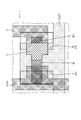
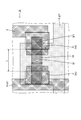
- FIG. 1 is a schematic plan view showing the configuration of the TFT portion of the TFT array substrate 1 of the first embodiment.
- the TFT array substrate 1 of Embodiment 1 is a circuit board in which a semiconductor element is disposed on a transparent substrate B.
- the semiconductor element includes a semiconductor film SF made of an oxide semiconductor film such as indium gallium zinc oxide.
- the TFT array substrate 1 is provided with an etching stopper film ES made of an insulating material so as to cover at least the central portion (channel region CH) of the semiconductor film SF.
- the TFT array substrate 1 is a conductor film composed of a source electrode s1, a source wiring s2, and a drain electrode s3 (an example of a second electrode), at least part of which is disposed on the etching stopper film ES.
- Source metal is provided.
- the etching stopper film ES is provided with an opening H that exposes a member below the etching stopper film ES.
- the opening H of the present embodiment has a rectangular shape in plan view of the substrate. In FIG.
- an etching stopper film ES is formed except for a rectangular portion surrounded by the opening H.
- the opening H (hs) shown on the left side is arranged so as to partially overlap the source electrode s1 in plan view of the substrate, and the opening shown on the right side.
- the portion H (hd) has a shape that partially overlaps with the drain electrode s3 in plan view of the substrate.
- the TFT array substrate 1 of this embodiment is used for a liquid crystal panel that operates in an FFS (Fringe Field Switching) mode, and includes a pair of electrodes (a common electrode and a pixel electrode described later).
- FFS Flexible Field Switching
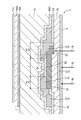
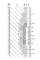
- FIG. 2 is a cross-sectional view taken along the line A-A ′ of FIG. 1, and schematically shows a cross-sectional configuration of the TFT array substrate 1 centering on the TFT portion.
- the TFT array substrate 1 is provided with a common electrode Com and a picture element electrode Pix that are stacked (opposed) to each other via a protective film PAS2.
- the common electrode Com is formed on the organic insulating film OI.
- the gate wiring g2 is disposed along the left-right direction of FIG.
- a gate electrode (an example of a first electrode) g1 is provided so as to branch from the gate wiring g2.
- the gate electrode g1 has a substantially rectangular shape in plan view of the substrate.
- Both the gate electrode g1 and the gate wiring g2 are composed of a gate metal (gate conductor film) G.
- the gate metal G is formed on a transparent substrate B made of a glass substrate or the like.
- a gate insulating film (an example of a first insulating film) GI is formed on the transparent substrate B so as to cover the gate metal G.
- a gate insulating film GI is also formed on the gate metal G.
- the semiconductor film SF is formed on the gate insulating film GI so as to be disposed above the gate electrode g1 in the gate metal G.
- the semiconductor film SF has a rectangular shape elongated in the left-right direction (arrangement direction of the gate wiring g2) in FIG.
- One end portion of the semiconductor film SF disposed on the right side (that is, the drain electrode s3 side) in each drawing is shaped to protrude outward from the gate electrode g1. That is, as shown in FIG. 1, the one end portion of the semiconductor film SF protrudes outside the peripheral edge (end portion) of the gate electrode g1 in a plan view of the substrate.
- This protruding portion may be particularly referred to as a protruding semiconductor film portion SF1.
- the protruding semiconductor film portion SF1 is directly covered with the drain electrode s3 in the conductor film (source metal) S.
- the other end portion of the semiconductor film SF disposed on the left side (that is, the source electrode s1 side) in each figure does not protrude outside the gate electrode g1, and the gate electrode g1 in a plan view of the substrate. It is in a shape that is retracted inward from the periphery.
- the end of the recessed semiconductor film SF is covered with the source electrode s1 and the source wiring s2 in the conductor film (source metal) S.
- the width W of the semiconductor film SF in the vertical direction (arrangement direction of the source wiring s2) in FIG. 1 is set smaller than the width in the vertical direction of the gate electrode g1. Further, the width W of the semiconductor film SF is set to be smaller than each width in the vertical direction of the source electrode s1 and the drain electrode s3.
- the etching stopper film ES is provided on the semiconductor film SF and the gate insulating film GI so as to cover at least the central portion (channel region CH) of the semiconductor film SF.
- 1 and 2 indicates the width of the etching stopper film ES that covers the central portion (channel region CH) of the semiconductor film SF (the width in the left-right direction in each figure), and the source electrode s1 This corresponds to the width of the channel region CH formed between the electrode and the drain electrode s3.
- the distance indicated by the symbol L also corresponds to the distance between adjacent openings H (hs, hd) formed in the etching stopper film ES.
- the opening H (hs) is provided so that the source electrode s1 can be stacked on the semiconductor film SF so as to be in direct contact with the semiconductor film SF.
- the opening H (hd) is provided so that the drain electrode s3 can be stacked on the semiconductor film SF (mainly, the protruding semiconductor film part SF1) so that the drain electrode s3 is in direct contact with the semiconductor film SF.
- the opening H (hd) on the drain electrode s3 side has an end portion of the semiconductor film SF that protrudes outward from the gate electrode g1 (the right end portion shown in each drawing, that is, the protruding semiconductor film portion SF1).
- the shape (size) is set so as to fit inside in a plan view. More specifically, the width of the opening H (hd) in the left-right direction (the arrangement direction of the gate wiring g2) is set so that the protruding semiconductor film portion SF1 is accommodated inside. From the opening H (hd), a portion of the surface of the semiconductor film SF (including the surface of the protruding semiconductor film portion SF1) that is not covered with the etching stopper film ES is exposed.
- the opening H (hs) on the source electrode s1 side is also smaller than the opening H (hd) on the drain side s3, but the other end of the semiconductor film SF (shown in each drawing).
- the shape (size) is set so that the left end portion is accommodated inside in the plan view of the substrate. From the opening H (hs), the surface of the portion of the semiconductor film SF that is not covered with the etching stopper film ES is exposed.
- the width of the opening H (hs, hd) in the vertical direction (the direction in which the source wiring s2 is disposed) is set so that the respective electrodes (source electrode s1, drain electrode s3) are generally accommodated in the substrate plan view. ing. Further, the width of the opening H (hs, hd) in the vertical direction (the arrangement direction of the source wiring s2) is set to be larger than the width W in the vertical direction of the semiconductor film SF. In the present embodiment, a part of the source wiring s2 is accommodated inside the opening H (hs). In addition, a substantially rectangular portion of the drain electrode s3 that faces the source electrode s1 across the channel region CH is accommodated inside the opening H (hd).
- the source wiring s2 is arranged so as to be orthogonal to the gate wiring g2 in plan view of the substrate.
- the source electrode s1 is provided so as to branch from the source line s2.
- the source electrode s1 has a shape partially climbing on the semiconductor film SF. Then, the portion that has ridden is stacked on the surface of the semiconductor film SF exposed from the inside of the opening H (hs).
- a drain electrode s3 is provided on the source electrode s1 and the semiconductor film SF so as to face each other while keeping a space therebetween.
- the drain electrode s3 also has a shape partially rising on the semiconductor film SF.
- the drain electrode s3 includes a stacked portion so as to be in direct contact with the surface of the semiconductor film SF exposed from the inside of the opening H (hd) (including the surface of the protruding semiconductor film portion SF1).
- the source electrode s1 and the drain electrode s3 protrude outward from the semiconductor film SF in the vertical direction of FIG. 1 (the arrangement direction of the source wiring s2).
- the end portion of the semiconductor film SF is recessed inwardly from the end portions of the source electrode s1 and the drain electrode s3 in the vertical direction (the arrangement direction of the source wiring s2).
- the protective film PAS1 is formed so as to cover the conductor film S (source electrode s1, source wiring s2, drain electrode s3, etc.).
- the organic insulating film OI, the common electrode Com, the protective film PAS2, and the pixel electrode Pix are sequentially stacked so as to cover the protective film PAS1.
- FIG. 3 is an explanatory view schematically showing an overlapping region C of the gate metal G, the semiconductor film SF, and the source metal (conductor film) S.
- FIG. 3 shows the same planar configuration of the TFT array substrate 1 as in FIG.
- the gate electrode (first electrode) g1 portion overlaps the semiconductor film SF and the source metal (conductor film) S through the gate insulating film (first insulating film) GI in plan view of the substrate. It is a part to do.
- the gate electrode g1 of the present embodiment is not entirely overlapped with the drain electrode, and has a shape (size) that does not partially overlap with the drain electrode s3. ing. Specifically, the gate electrode g1 of the present embodiment is set to have a width (particularly on the drain electrode s3 side) narrower in at least the left-right direction (arrangement direction of the gate wiring g2) than the conventional gate electrode. . As described above, in the TFT array substrate 1 of the present embodiment, the overlapping region C of the gate metal G, the semiconductor film SF, and the source metal (conductor film) S is set narrower than the conventional one. It can be said that the capacitance between the electrode g1 and the drain electrode s3 (Cgd capacitance) is reduced.
- a liquid crystal display device (not shown) equipped with a liquid crystal panel including the TFT array substrate 1 includes a backlight device as a light source.
- the liquid crystal panel mainly includes a TFT array substrate 1, a counter substrate (color filter substrate) facing the TFT array substrate 1, and a liquid crystal layer sandwiched between these substrates.
- the backlight device supplies light BL toward the TFT array substrate 1.
- the light BL supplied from the backlight device travels from the transparent substrate B side of the TFT array substrate 1 toward the liquid crystal layer side.
- the semiconductor film SF is disposed above the gate electrode (first electrode) g1 and overlaps with the gate electrode g1 in plan view of the substrate.
- the end portion of the semiconductor film SF that is, the protruding semiconductor film portion SF1
- the end portion of the semiconductor film SF protrudes outside the gate electrode g1.
- the light BL toward the gate electrode g1 is blocked by the gate electrode g1. Therefore, most of the semiconductor film SF arranged so as to overlap above the gate electrode g1 is shielded from light by the gate electrode g1, so that the light BL is not directly applied.
- some of the light BL supplied from the backlight device is directed toward the semiconductor film SF (protruding semiconductor film portion SF1) protruding outward from the gate electrode g1.
- Such light BL passes through the transparent substrate B and the gate insulating film (first insulating film) GI, and protrudes to reach the semiconductor film portion SF1.
- a drain electrode s3 made of a conductor film (source metal) S is stacked on the protruding semiconductor film portion SF1 so as to be in direct contact therewith.
- the drain electrode s3 is stacked not only on the surface of the protruding semiconductor film portion SF1 but also on the surface of the semiconductor film SF exposed from the opening H (hd).
- the protruding semiconductor film portion SF1 is electrically connected to the drain electrode s3, and an etching stopper film ES made of an insulating material is interposed between the protruding semiconductor film portion SF1 and the drain electrode s3. It has not been done.
- the generated charge contacts the protruding semiconductor film part SF1 from the protruding semiconductor film part SF1. It can move to the drain electrode s3.
- the light BL is exposed to the protruding semiconductor film portion SF1 of the semiconductor film SF, accumulation of electric charges in the semiconductor film SF is suppressed, and as a result, deterioration of the function of the semiconductor film SF is suppressed.
- the function deterioration of the semiconductor film SF is suppressed while the Cgd capacitance is reduced.
- FIG. 4 is a schematic cross-sectional view of the substrate after the formation of the gate metal G, corresponding to a cross section taken along line AA ′ of FIG.
- a gate metal G including a gate electrode (first electrode) g1
- the step of forming the gate metal G can be formed, for example, by forming a layered gate metal G on the transparent substrate B and then patterning it into a desired shape by a photolithography method.
- a resist having a predetermined pattern is formed on the layered gate metal G by a mask process, and then the layered gate metal G is etched to form a patterned gate metal G. Is done. Thereafter, the resist is removed.
- FIG. 5 is a schematic cross-sectional view of the substrate after forming the gate insulating film GI and the semiconductor film SF, corresponding to the cross section taken along the line AA ′ of FIG.
- the gate insulating film (first insulating film) GI is formed.
- the gate insulating film GI is made of, for example, a silicon nitride (SiN x ) film, a silicon oxide (SiO 2 ) film, or the like, and can be formed by a plasma enhanced chemical vapor deposition (PECVD) method or the like.
- PECVD plasma enhanced chemical vapor deposition
- the gate insulating film GI may be a single layer or a laminate of two or more layers.
- an island-shaped semiconductor film SF made of an oxide semiconductor such as indium gallium zinc oxide is formed on the gate insulating film GI.
- the island-shaped semiconductor film SF is formed by depositing an oxide semiconductor material into a film shape (film thickness: 10 nm to 300 nm) by using, for example, a sputtering method, and then forming a desired film using a photolithography method. It can be formed by patterning the film into a shape.
- FIG. 6 is a schematic cross-sectional view of the substrate after the formation of the etching stopper film ES corresponding to the cross section taken along the line AA ′ of FIG.
- the etching stopper film ES is formed by plasma CVD (for example) using an insulating material including silicon (for example, a silicon oxide film (SiO 2 ), a silicon nitride film (SiN x ), a silicon nitride oxide film (SiNO)), or the like.
- etching stopper film ES is provided with openings H (hs, hd). The etching stopper film ES is formed so as to cover at least the central portion (channel region CH) with respect to the island-shaped semiconductor film SF.
- the etching stopper film ES is provided in the above-described form in order to maintain the reliability of the TFT array substrate 1 provided with the semiconductor film SF.
- the etching stopper film ES is set so as not to cover the protruding semiconductor film portion SF1. Therefore, the shape and size of the opening H (hd) are set so that the protruding semiconductor film portion SF1 is accommodated inside.
- the central portion (channel region CH) of the semiconductor film SF is disposed in a plan view of the substrate. Yes.
- FIG. 7 is a schematic cross-sectional view of the substrate after the formation of the conductor film (source metal) S, corresponding to the cross section taken along the line A-A ′ of FIG.
- the conductor constituting the conductor film (source metal) S is exposed from the etching stopper film ES and the openings H (hs, hd). Is deposited in layers.
- a resist is formed on the layered (film-like) conductor (deposit) by a mask process, and then the conductor is etched.
- the layered (film-like) conductor is patterned by wet etching or the like.
- a conductor film (source metal) S composed of the source electrode s1, the source wiring s2, the drain electrode s3, and the like is formed from the layered conductor.
- the resist on the substrate is appropriately removed.
- the formation process of the conductor film S by wet etching. It is possible to reduce the manufacturing cost of the TFT array substrate 1 by patterning by wet etching.
- an etchant used for wet etching for example, it is used for a source metal which is a superaqueous etching solution (Cu / Ti laminate (indicating that Cu is an upper layer and Ti is a lower layer)). And a mixed solution of phosphoric acid + nitric acid + acetic acid (used for a source metal that is a laminate of Mo / Al / Mo, etc., a general etching solution of Al), and the like. Thereby, even if the source metal is a laminated body, the source metal can be etched in a lump.
- the drain electrode s3 is in direct contact with the semiconductor film SF (including the protruding semiconductor film part SF1) exposed from the opening H (hd). Laminated.
- FIG. 8 is a schematic cross-sectional view of the substrate after the formation of the protective film PAS1 and the organic insulating film OI corresponding to the cross section taken along the line AA ′ of FIG.
- the protective film PAS1 is, for example, a silicon nitride (SiN x ) film, a silicon oxide (SiO 2 ) film, or the like, and can be formed by a plasma induced chemical vapor deposition (PECVD) method or the like.
- PECVD plasma induced chemical vapor deposition
- an organic insulating film OI is formed on the protective film PAS1.
- the organic insulating film OI is made of, for example, an acrylic resin and can be formed by a spin coating method or the like. Note that by forming the organic insulating film OI, the substrate can be planarized as shown in FIG.
- FIG. 9 is a schematic cross-sectional view of the substrate after formation of the common electrode Com, corresponding to a cross-section along the line A-A ′ of FIG.
- the electrode material constituting the common electrode Com is deposited in layers using the sputtering method on the entire surface of the organic insulating film OI.
- transparent electrode materials such as ITO (indium tin oxide) and IZO (indium zinc oxide), are used, for example.
- ITO indium tin oxide
- IZO indium zinc oxide
- FIG. 10 is a schematic cross-sectional view of the substrate after the formation of the protective film PAS2, corresponding to the cross section taken along the line AA ′ of FIG.
- the protective film PAS2 is formed on the common electrode Com.
- the protective film PAS2 is made of, for example, a silicon nitride (SiN x ) film or the like, as with the protective film PAS1 described above, and can be formed by a plasma induced chemical vapor deposition (PECVD) method or the like.
- PECVD plasma induced chemical vapor deposition
- an electrode material constituting the pixel electrode Pix is deposited in layers on the protective film PAS2 using a sputtering method.
- a transparent electrode material transparent conductive film
- ITO indium tin oxide
- IZO indium zinc oxide
- the pixel electrode Pix is connected to the drain electrode s3 through a contact hole (not shown). Therefore, an opening (contact hole) necessary for connecting the pixel electrode Pix to the drain electrode s3 is provided in the common electrode Com, the organic insulating film OI, and the like so as to penetrate in the thickness direction.
- the TFT array substrate 1 is appropriately provided with an alignment film that regulates the alignment of liquid crystal molecules in the liquid crystal layer, a polarizing plate disposed outside the transparent substrate, an optical film, and the like.
- the conductor film S is made of source metal.
- the source metal corresponds to the source wiring s2 and members (source electrode s1, drain electrode s3, etc.) formed by the same process as the source wiring s2.
- the conductor film S is made of, for example, a metal laminate such as a Cu / Ti laminate or a Mo / Al / Mo laminate.
- a metal laminate such as a Cu / Ti laminate or a Mo / Al / Mo laminate.
- said conductor film S what contains an aluminum layer, an aluminum alloy layer, a copper layer, and a copper alloy layer other than them can be used suitably.
- the aluminum layer is a layer substantially composed only of aluminum metal.
- an element may diffuse from another metal material or an interlayer insulating film that is in contact with the aluminum layer. Therefore, a trace amount of impurity element may be included in the aluminum layer.
- the aluminum alloy layer may contain aluminum as an essential component, and may include other metal elements and non-metal elements such as silicon. Examples of the metal element added to the aluminum alloy include nickel, iron, cobalt, and the like. It is more preferable to add boron, neodymium, lanthanum, or the like as an additional element to the aluminum alloy.
- the copper layer is a layer substantially made only of copper.
- the copper layer may contain a trace amount of an impurity element because the element may diffuse from another metal material in contact with the copper layer, the protective film PAS1, or the like.
- the copper alloy layer may contain copper as an essential component, and may further include other metal elements and nonmetal elements such as carbon and silicon. Examples of the metal element added to the copper alloy include magnesium and manganese.
- the wiring includes a signal wiring for transmitting an electric signal, a power supply line for supplying power, a wiring for forming a circuit, a wiring for applying an electric field (for example, applying an electric field to the gate of the TFT), and the like. Further, when the TFT array substrate 1 of the present embodiment is applied to a liquid crystal display device (an example of a display device), the TFT array substrate of the present embodiment has an auxiliary capacitor used for holding a voltage applied to the liquid crystal. A storage capacitor wiring to be formed may be further provided.
- the semiconductor element is preferably a thin film transistor (TFT) as described above.
- the source line s2 is electrically connected to the pixel electrode Pix constituting the display pixel via the source electrode s1 and the drain electrode s3 constituting the TFT.
- the transparent substrate B is not particularly limited, and various substrates can be used.
- a substrate such as a single crystal semiconductor substrate, an oxide single crystal substrate, a metal substrate, a glass substrate, a quartz substrate, or a resin substrate can be used.
- a conductive substrate such as a single crystal semiconductor substrate or a metal substrate, it is preferable to use an insulating film or the like provided thereon.
- the TFT array substrate 1 according to the first embodiment is disassembled, and a liquid crystal panel (STEM (Scanning Transmission Electron Microscope), SEM (Scanning Transmission Electron Microscope), etc. is observed with a microscope such as a liquid crystal panel (scanning transmission electron microscope). The pattern shape of the liquid crystal cell) can be confirmed.
- STEM Sccanning Transmission Electron Microscope
- SEM Sccanning Transmission Electron Microscope
- the TFT array substrate (semiconductor device) 1 of the present embodiment includes the transparent substrate (substrate) B, the gate electrode (first electrode) g1 formed on the transparent substrate B, and the gate electrode (first electrode). Electrode) g1 and a gate insulating film (first insulating film) GI formed across the gate electrode (first electrode) g1 and the transparent substrate B and an oxide semiconductor film, and has a channel region CH.
- the semiconductor film SF formed on the gate insulating film GI is overlapped with the gate electrode g1 in a state where the end portion (excess semiconductor film portion) SF1 protrudes outside the gate electrode g1.
- a drain electrode (second electrode) s3 stacked on the semiconductor film SF.
- the light passes through the gate insulating film GI and passes through the gate electrode g1.
- the gate electrode g1 There are those that protrude outward from the semiconductor film portion SF1. Since the protruding semiconductor film portion SF1 does not overlap with the gate electrode g1, it is a portion directly exposed to light.
- the drain electrode s3 since the drain electrode s3 is laminated on the semiconductor film SF so as to cover the surface of the semiconductor film SF exposed from the opening H (hd), the protruding semiconductor film part SF1 and The drain electrode s3 is in contact with each other and is electrically connected.
- the semiconductor film SF has a shape in which a portion other than the protruding semiconductor film portion SF1 is accommodated in the gate electrode g1 when viewed in plan.
- the semiconductor film SF has a shape in which a portion other than the protruding semiconductor film portion SF1 is accommodated in the gate electrode g1 when viewed in plan.
- the semiconductor film SF has a shape in which a portion other than the protruding semiconductor film portion SF1 is accommodated in the gate electrode g1 when viewed in plan, light is emitted to the portion (a portion other than the protruding semiconductor film portion SF1). It is suppressed that the function of the semiconductor film SF is reduced.
- the semiconductor film SF has a longitudinal shape extending along the protruding direction of the protruding semiconductor film portion SF1 (arrangement direction of the gate wiring g2) when viewed in plan.
- the portion where the drain electrode s3 is stacked has a shape that fits in the drain electrode s3.
- the semiconductor film SF has a substantially rectangular shape extending in the left-right direction (arrangement direction of the gate wiring g2) in each figure in a plan view of the substrate.
- an end portion on the opposite side of the protruding semiconductor film portion SF1 has a shape that fits in the source electrode s1 and the source wiring s2 in a plan view of the substrate.
- FIG. 11 is a schematic plan view showing the configuration of the TFT portion of the TFT array substrate 1A of the second embodiment.
- the size of the opening H (hs, hd) provided in the etching stopper film ES is set smaller than that of the first embodiment.
- the opening H (hs, hd) of the present embodiment also has a vertically long rectangular shape in plan view of the substrate.
- the opening H (hs, hd) of the present embodiment is set to have a length in the vertical direction (arrangement direction of the source wiring s2) in FIG.
- the length in the vertical direction of the opening H (hs, hd) is set slightly larger than the length (width) in the vertical direction of the source electrode s1 and the drain electrode s3 of the conductor film S.
- the length of the opening H (hs, hd) in the present embodiment in the left-right direction (arrangement direction of the gate wiring g2) in FIG. 11 is the same as that in the first embodiment. That is, the protruding semiconductor film portion SF1 of the semiconductor film SF is accommodated inside the opening H (hd) of the present embodiment.
- the etching stopper film ES made of an insulating material is interposed between the drain electrode s3 and the semiconductor film SF (mainly the protruding semiconductor film portion SF1).
- the drain electrode s3 and the semiconductor film SF (mainly the protruding semiconductor film part SF1) are stacked in direct contact with each other.
- the etching stopper film ES is not interposed between the drain electrode s3 and the semiconductor film SF (mainly protruding semiconductor film portion SF1), and the drain electrode s3 and the semiconductor film SF (mainly protruding).
- the shape of the opening H (hd) may be changed as appropriate as long as the semiconductor film portion SF1) is stacked in direct contact with the semiconductor film portion SF1).
- the TFT array substrate 1A of the present embodiment also has a reduced Cgd capacitance and a reduced function of the semiconductor film SF.
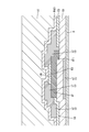
- FIG. 12 is a schematic cross-sectional view centering on the TFT portion in the TFT array substrate 1B of the third embodiment.
- the TFT array substrate 1B of this embodiment is suitably used for a liquid crystal display device (not shown) in a vertical alignment (VA) mode.
- VA vertical alignment
- the configuration of most of the TFT array substrate 1B of the present embodiment is the same as that of the first embodiment. Therefore, the manufacturing process in the TFT array substrate 1B of the present embodiment is basically the same as that of the above-described first embodiment until the step of forming the organic insulating film OI.
- the configuration of the TFT array substrate 1B of the present embodiment will be described below while explaining the manufacturing process after the formation of the organic insulating film OI.
- the configurations (materials and the like) other than explicitly indicating each member are the same as those described above.
- the pixel electrode Pix is formed on the entire surface of the organic insulating film OI after the organic insulating film OI is formed.
- a transparent electrode material transparent conductive film
- ITO indium tin oxide
- IZO indium zinc oxide
- the length of the opening H (hs, hd) of this embodiment in the left-right direction (arrangement direction of the gate wiring g2) in FIG. 12 is the same as that of the first embodiment. That is, the end portion (the protruding semiconductor film portion SF1) of the semiconductor film SF on the drain electrode s3 side is accommodated inside the opening portion H (hd) of the present embodiment. Therefore, also in the present embodiment, when the conductor film S is formed, the etching stopper film ES made of an insulating material is interposed between the drain electrode s3 and the semiconductor film SF (mainly the protruding semiconductor film portion SF1).
- the drain electrode s3 and the semiconductor film SF are stacked in direct contact with each other. For this reason, in the TFT array substrate 1B of the present embodiment, as in the first embodiment, the Cgd capacitance is reduced and the functional degradation of the semiconductor film SF is suppressed.
- the shape of the opening H of the etching stopper film ES is a rectangular shape in plan view of the substrate, but is not particularly limited as long as it is a through hole.
- the semiconductor film in which the oxide semiconductor is indium gallium zinc oxide is used in the above embodiment, the present invention is not limited to this.
- the semiconductor element (TFT unit) is used for the display unit of the TFT array substrate.
- the present invention is not limited to this, and in other embodiments, for example, the TFT array substrate
- the semiconductor element (TFT portion) having the above-described configuration may be applied to a monolithic gate driver.
- the array substrate used for the liquid crystal panel is exemplified as the semiconductor device.
- other devices such as an organic EL device, an inorganic EL device, and an electrophoretic device are used. It may be a semiconductor device to be used.
- SYMBOLS 1,1A, 1B TFT array substrate (semiconductor device), B ... Transparent substrate (substrate), BL ... Light, C ... Overlapping region, CH ... Channel region, Com ... Common electrode, ES ... Etching stopper film, G ... Gate Metal, g1 ... gate electrode (first electrode), g2 ... gate wiring, GI ... gate insulating film (first insulating film), H ... opening, hs ... opening on the source electrode side, hd ... opening on the drain electrode side Part, SF ... semiconductor film, SF1 ... protruding semiconductor film part, L ... width of channel region (between openings), PAS1 ... protective film, PAS2 ... protective film, Pix ... pixel electrode, S ... conductor film (source metal) ), S1... Source electrode, s2... Source wiring, s3... Drain electrode (second electrode), W.
- G ... Gate Metal g1 ... gate electrode (first electrode),
Landscapes
- Physics & Mathematics (AREA)
- Nonlinear Science (AREA)
- Mathematical Physics (AREA)
- Chemical & Material Sciences (AREA)
- Crystallography & Structural Chemistry (AREA)
- General Physics & Mathematics (AREA)
- Optics & Photonics (AREA)
- Engineering & Computer Science (AREA)
- Microelectronics & Electronic Packaging (AREA)
- Geometry (AREA)
- Thin Film Transistor (AREA)
Abstract
本発明に係る半導体装置1は、基板B上に形成される第1電極G(g1)と、第1電極g1を覆う第1絶縁膜GIと、チャネル領域CHを有し、平面視した際、端部SF1が第1電極g1よりも外側にはみ出した状態で第1電極g1と重畳するように、第1絶縁膜GI上に形成される半導体膜SFと、チャネル領域CHを覆う形で半導体膜SF及び第1絶縁膜GIに亘って形成される絶縁性の膜からなり、平面視した際、半導体膜SFの前記端部SF1が内側に収まり、かつチャネル領域CHに隣接した半導体膜SFの表面を露出させる開口部H(hd)を含むエッチングストッパ膜ESと、開口部H(hd)から露出する半導体膜SFの前記表面を覆うように、半導体膜SF上に積層される第2電極S(s3)とを備える。
Description
本発明は、半導体装置、及び表示装置に関する。
薄膜トランジスタ(TFT:Thin Film Transistor)等の半導体素子を含む回路基板等の半導体装置は、液晶表示装置、エレクトロルミネセンス表示装置、及び電気泳動を用いる表示装置等の電子装置の構成部材として汎用されている。
以下、TFT駆動の液晶パネルを構成するTFTアレイ基板の回路構成を例に挙げて説明する。TFTアレイ基板は、通常、m行の走査線とn列の信号線とからなるm×nマトリクス配線の交点に、スイッチング素子であるTFTが設けられた構成を含む画素回路を有する。なお、TFTのドレイン電極は、絵素電極と電気的に接続されている。また、走査ドライバIC(Integrated Circuit)やデータドライバIC等の周辺回路が、それぞれTFTから延びたゲート配線やソース配線と電気的に接続されている。
回路は、一般的に、TFTアレイ基板上に作り込まれるTFTの性能に影響を受ける。TFTアレイ基板上に作り込まれるTFTの性能は、その材質によって異なるので、回路基板上に作られるTFTにより回路が動作可能であるか、回路規模が大きくならないか、歩留まりが低下しないか等が、TFTアレイ基板上に作られる回路に影響する。従来の半導体装置(回路基板)では、TFTを安価かつ容易に形成することができる点からa-Si(アモルファスシリコン)が多く採用されている。
一方で、アモルファスシリコン半導体膜の代わりに、酸化物半導体膜を形成する半導体装置の製造方法が開示されている(例えば、特許文献1参照)。
(発明が解決しようとする課題)
a-Siに代わり、移動度が高いという利点をもつ酸化物半導体(例えば、インジウムガリウム亜鉛酸化物)を含む半導体素子を備えた半導体装置が検討されている。ここで、本発明者らは、信頼性の観点から酸化物半導体の少なくとも中央部分(チャネル領域)上にエッチングストッパ層(膜)を設けるエッチングストッパプロセス(以下、ESプロセスと称する場合がある)を使用することを検討している。
a-Siに代わり、移動度が高いという利点をもつ酸化物半導体(例えば、インジウムガリウム亜鉛酸化物)を含む半導体素子を備えた半導体装置が検討されている。ここで、本発明者らは、信頼性の観点から酸化物半導体の少なくとも中央部分(チャネル領域)上にエッチングストッパ層(膜)を設けるエッチングストッパプロセス(以下、ESプロセスと称する場合がある)を使用することを検討している。
ところで、近年、小型の液晶パネルで高精細化(例えば、300dpi(dots per inch)以上)が要求されている。液晶パネルの精細度が高くかつ絵素電極が小さい場合、液晶パネル全体の総容量は低下する。その一方で、ゲート電極-ドレイン電極間容量(Cgd容量)は略一定であるため、総容量に占めるCgd容量の割合が大きくなる。なお、Cgd容量は、基本的には絶縁層を介して対向するゲートメタルと、半導体層(膜)及びソースメタルとの間で形成される。
ESプロセスを使用した液晶パネルのCgd容量は、バックチャネルエッチ(back-channel-etch)方式を用いた液晶パネル(CE構造の液晶パネル)のCgd容量に比べて大きくなる傾向がある。ESプロセスを使用した液晶パネルであって、例えば小型のもの等において、Cgd容量を好適に低減し、これによりCgd容量による印加電圧への影響を低減し、設定通りの電圧を適切に印加できるものとし、例えば、半導体装置(回路基板)を備える表示装置の表示性能を良好なものとすることが望まれるところであった。
Cgd容量を低減する方法としては、例えば、基板平面視で、ゲートメタルが半導体層及びソースメタルに対して重畳する部分を少なくするために、ゲートメタルの形状を小さく設定することが検討されている。その場合、基板平面視で、半導体層の一部がゲートメタルよりも外側にはみ出す形となる。
ところで、ゲートメタルは、Cgd容量を形成する原因となっているものの、バックライト装置から液晶パネル(TFTアレイ基板)に向けて供給される光が半導体層に当たるのを防止する(つまり、遮光する)機能も担っている。そのため、上記のように、ゲートメタルの形状が小さく設定されると、基板平面視で、ゲートメタルから外側にはみ出した部分の半導体層に、バックライトからの光が当たることになる。半導体層に光が当たると、半導体層の機能が低下してしまう。特に、半導体層が、酸化物半導体からなる場合、光による機能低下が著しく問題となっている。
半導体層(半導体膜)は、TFTアレイ基板において、ゲートメタル上を覆うゲート絶縁層と、絶縁性であるエッチングストッパ層(膜)とで挟まれた状態にある。このような半導体層にバックライト装置からの光が当たると、半導体層で化学反応が生じて半導体層に電荷が蓄積されるため、半導体層の機能が低下すると考えられる。
本発明は、上記現状に鑑みてなされたものであり、Cgd容量が低減されつつ、酸化物半導体からなる半導体膜の機能低下が抑制された半導体装置、及び前記半導体装置を備えた表示装置を提供することを目的とする。
(課題を解決するための手段)
本発明に係る半導体装置は、基板と、前記基板上に形成される第1電極と、前記第1電極を覆う形で前記第1電極及び前記基板に亘って形成される第1絶縁膜と、酸化物半導体の膜からなり、チャネル領域を有し、平面視した際、端部が前記第1電極よりも外側にはみ出した状態で前記第1電極と重畳するように、前記第1絶縁膜上に形成される半導体膜と、前記チャネル領域を覆う形で前記半導体膜及び前記第1絶縁膜に亘って形成される絶縁性の膜からなり、平面視した際、前記半導体膜の前記端部が内側に収まり、かつ前記チャネル領域に隣接した前記半導体膜の表面を露出させる開口部を含むエッチングストッパ膜と、前記開口部から露出する前記半導体膜の前記表面を覆うように、前記半導体膜上に積層される第2電極と、を備える。
本発明に係る半導体装置は、基板と、前記基板上に形成される第1電極と、前記第1電極を覆う形で前記第1電極及び前記基板に亘って形成される第1絶縁膜と、酸化物半導体の膜からなり、チャネル領域を有し、平面視した際、端部が前記第1電極よりも外側にはみ出した状態で前記第1電極と重畳するように、前記第1絶縁膜上に形成される半導体膜と、前記チャネル領域を覆う形で前記半導体膜及び前記第1絶縁膜に亘って形成される絶縁性の膜からなり、平面視した際、前記半導体膜の前記端部が内側に収まり、かつ前記チャネル領域に隣接した前記半導体膜の表面を露出させる開口部を含むエッチングストッパ膜と、前記開口部から露出する前記半導体膜の前記表面を覆うように、前記半導体膜上に積層される第2電極と、を備える。
前記半導体装置において、第1電極が基板上に形成されており、第1絶縁膜が、前記第1電極を覆う形で前記第1電極及び前記基板に亘って形成されている。そして、酸化物半導体の膜からなる半導体膜は、平面視した際、端部が前記第1電極よりも外側にはみ出した状態で前記第1電極と重畳するように、前記第1絶縁膜上に形成されている。前記半導体膜は、チャネル領域を有しており、そのチャネル領域を覆う形で前記半導体膜及び前記第1絶縁膜に亘って絶縁性の膜からなるエッチングストッパ膜が形成されている。前記エッチングストッパ膜は、平面視した際、前記半導体膜の前記端部が内側に収まり、かつ前記チャネル領域に隣接した前記半導体膜の表面を露出させる開口部を備えている。そして、前記開口部から露出する前記半導体膜の前記表面を覆うように、前記半導体膜上に第2電極が積層されている。このような構成を備えた前記半導体装置に対して、前記基板側から光が供給された場合、その光の中には、前記第1絶縁膜を通過して、前記第1電極よりも外側にはみ出している前記半導体膜の前記端部に向かうものがある。前記半導体膜の前記端部は、前記第1電極と重畳していないため、直接、光が当たる部分となっている。ただし、前記半導体装置においては、前記開口部から露出する前記半導体膜の前記表面を覆うように、前記半導体膜上に第2電極が積層されているため、前記半導体膜の前記端部と第2電極とが互いに接触して電気的に接続された状態となっている。そのため、前記半導体膜の前記端部に光が当たって光反応が生じても、生成した電荷は、前記半導体膜の前記端部から前記半導体膜の前記端部に接触している前記第2電極へ移動することができる。その結果、平面視した際、前記第1電極によって覆われていない前記半導体膜の前記端部に光が当たっても、前記半導体膜に電荷が蓄積されることが抑制され、ひいては、前記半導体膜の機能低下が抑制されることになる。
前記半導体装置において、前記半導体膜は、平面視した際、前記端部以外の部分が前記第1電極内に収まる形をなしているものであってもよい。前記基板側から前記半導体装置に向けて光が供給された場合、その光が前記端部以外の前記半導体膜の部分に向かっても、その部分は前記第1電極と重畳しているため、前記光は前記第1電極によって遮られることになる。したがって、前記半導体膜が、平面視した際、前記端部以外の部分が前記第1電極内に収まる形をなしていると、前記部分に光が当たって前記半導体膜の機能が低下することが抑制される。
前記半導体装置において、前記半導体膜は、平面視した際、前記端部がはみ出す方向に沿って延びた長手状をなし、かつ前記第2電極が積層されている部分は、前記第2電極内に収まる形をなしているものであってもよい。
前記半導体装置において、前記第1電極は、ゲート電極からなり、前記第2電極は、ドレイン電極からなるものであってもよい。
前記半導体装置において、前記第1電極は、ゲート配線から分岐する形で設けられているものであってもよい。
前記半導体装置において、平面視した際、前記チャネル領域を挟んで前記第2電極と対向するように、前記半導体膜上に積層されるソース電極を備えるものであってもよい。
前記半導体装置において、前記第2電極は、前記ソース電極と同じ導電性材料からなるものであってもよい。
前記半導体装置において、前記半導体膜が、酸化インジウムガリウム亜鉛からなるものであってもよい。
本発明に係る表示装置は、前記半導体装置と、前記半導体装置と対向するように配置された対向基板と、前記半導体装置と前記対向基板との間に配置された液晶層とを備える。
前記表示装置において、前記半導体装置に向けて光を供給するバックライト装置を備えるものであってもよい。
(発明の効果)
本発明によれば、Cgd容量が低減されつつ、酸化物半導体からなる半導体膜の機能低下が抑制された半導体装置、及び前記半導体装置を備えた表示装置を提供することができる。
本発明によれば、Cgd容量が低減されつつ、酸化物半導体からなる半導体膜の機能低下が抑制された半導体装置、及び前記半導体装置を備えた表示装置を提供することができる。
<実施形態1>
(TFTアレイ基板)
本発明の実施形態1を、図1から図10を参照しつつ説明する。本実施形態では、バックライト装置を備えた液晶表示装置(表示装置の一例)に利用されるTFTアレイ基板(半導体装置の一例)1を例示する。図1は、実施形態1のTFTアレイ基板1のTFT部の構成を示す平面模式図である。実施形態1のTFTアレイ基板1は、透明基板B上に半導体素子が配置された回路基板である。半導体素子は、インジウムガリウム亜鉛酸化物等の酸化物半導体の膜からなる半導体膜SFを含んでいる。
(TFTアレイ基板)
本発明の実施形態1を、図1から図10を参照しつつ説明する。本実施形態では、バックライト装置を備えた液晶表示装置(表示装置の一例)に利用されるTFTアレイ基板(半導体装置の一例)1を例示する。図1は、実施形態1のTFTアレイ基板1のTFT部の構成を示す平面模式図である。実施形態1のTFTアレイ基板1は、透明基板B上に半導体素子が配置された回路基板である。半導体素子は、インジウムガリウム亜鉛酸化物等の酸化物半導体の膜からなる半導体膜SFを含んでいる。
TFTアレイ基板1は、半導体膜SFの少なくとも中央部分(チャネル領域CH)を覆うように、絶縁材料から構成されるエッチングストッパ膜ESが配置される。また、TFTアレイ基板1は、前記エッチングストッパ膜ES上にその少なくとも一部が配置された、ソース電極s1、ソース配線s2及びドレイン電極s3(第2電極の一例)から構成される導電体膜(ソースメタル)Sを備える。エッチングストッパ膜ESには、その下側にある部材を露出させる開口部Hが設けられている。本実施形態の開口部Hは、基板平面視で、矩形状をなしている。図1において、開口部Hで囲まれる矩形の個所以外は、エッチングストッパ膜ESが形成されている。図1に示される2つの開口部Hのうち、左側に示される開口部H(hs)は、基板平面視でソース電極s1と部分的に重畳する形で配されており、右側に示される開口部H(hd)は、基板平面視でドレイン電極s3と部分的に重畳する形となっている。
本実施形態のTFTアレイ基板1は、FFS(Fringe Field Switching)モードで動作する液晶パネルに利用されるものであり、一対の電極(後述する共通電極及び画素電極)を備えている。なお、説明の便宜上、図1では、前記一対の電極等は省略されている。図2は、図1のA-A’線断面図であり、TFT部を中心としたTFTアレイ基板1の断面構成が模式的に示されている。図2に示されるように、TFTアレイ基板1には、共通電極Comと絵素電極Pixとが保護膜PAS2を介して互いに積層(対向)する形で設けられている。なお、共通電極Comは、有機絶縁膜OI上に形成されている。
ゲート配線g2は、図1に示されるように、図1の左右方向に沿って配設されている。このゲート配線g2から分岐する形でゲート電極(第1電極の一例)g1が設けられている。ゲート電極g1は、基板平面視で略矩形状をなしている。ゲート電極g1及びゲート配線g2は、共にゲートメタル(ゲート導電体膜)Gから構成されている。ゲートメタルGは、ガラス基板等からなる透明基板B上に形成されている。図2に示されるように、ゲートメタルGを覆う形でゲート絶縁膜(第1絶縁膜の一例)GIが透明基板B上に形成されている。ゲートメタルG上にも、ゲート絶縁膜GIが形成されている。
半導体膜SFは、図2に示されるように、ゲートメタルGにおけるゲート電極g1の上方に配される形で、ゲート絶縁膜GI上に形成されている。図1に示されるように、半導体膜SFは、基板平面視で、図1の左右方向(ゲート配線g2の配設方向)に細長く延びた矩形状をなしている。各図の右側(つまり、ドレイン電極s3側)に配される半導体膜SFの一方の端部は、ゲート電極g1よりも外側にはみだす形となっている。つまり、図1に示されるように、基板平面視でゲート電極g1の周縁(端部)よりも外側に半導体膜SFの前記一方の端部がはみ出した状態となっている。このはみ出した部分のことを、特に、はみ出し半導体膜部SF1と称する場合がある。このはみ出し半導体膜部SF1は、導電体膜(ソースメタル)Sのうち、ドレイン電極s3によって直接、覆われる。
これに対して、各図の左側(つまり、ソース電極s1側)に配される半導体膜SFの他方の端部は、ゲート電極g1よりも外側にはみ出さずに、基板平面視でゲート電極g1の周縁よりも内側に引っ込んだ形となっている。なお、この引っ込んだ形の前記半導体膜SFの端部は、本実施形態の場合、導電体膜(ソースメタル)Sのうち、ソース電極s1及びソース配線s2によって覆われる。
また、図1の上下方向(ソース配線s2の配設方向)における半導体膜SFの幅Wは、ゲート電極g1の前記上下方向における幅よりも小さく設定されている。また、半導体膜SFの幅Wは、ソース電極s1及びドレイン電極s3の前記上下方向における各幅よりも小さく設定されている。
エッチングストッパ膜ESは、少なくとも半導体膜SFの中央部分(チャネル領域CH)を覆う形で、半導体膜SF上及びゲート絶縁膜GI上に設けられている。図1及び図2において符号Lで示される距離は、半導体膜SFの中央部分(チャネル領域CH)を覆うエッチングストッパ膜ESの幅(各図の左右方向の幅)を示しており、ソース電極s1とドレイン電極s3との間に形成されるチャネル領域CHの幅に相当する。なお、前記符号Lで示される距離は、エッチングストッパ膜ESに形成されている隣り合った開口部H(hs,hd)間の距離にも対応している。
開口部H(hs)は、ソース電極s1が半導体膜SFと直に接触する形で、半導体膜SF上に積層できるように設けられている。また、開口部H(hd)は、ドレイン電極s3が、半導体膜SFと直に接触する形で、半導体膜SF(主として、はみ出し半導体膜部SF1)上に積層できるように設けられている。
ドレイン電極s3側の開口部H(hd)は、ゲート電極g1よりも外側にはみ出している半導体膜SFの端部(各図に示される右側端部、つまり、はみ出し半導体膜部SF1)が、基板平面視で内側に収まるように形状(大きさ)が設定されている。より詳細には、開口部H(hd)の左右方向(ゲート配線g2の配設方向)における幅が、前記はみ出し半導体膜部SF1が内側に収まるように設定されている。開口部H(hd)からは、エッチングストッパ膜ESで覆われていない部分の半導体膜SFの表面(はみ出し半導体膜部SF1の表面を含む)が露出している。
なお、本実施形態の場合、ソース電極s1側の開口部H(hs)も、ドレイン側s3の開口部H(hd)よりは小さいものの、半導体膜SFの他方の端部(各図に示される左側端部)が、基板平面視で内側に収まるように形状(大きさ)が設定されている。そして、開口部H(hs)からは、エッチングストッパ膜ESで覆われていない部分の半導体膜SFの表面が露出している。
また、開口部H(hs,hd)の上下方向(ソース配線s2の配設方向)における幅は、基板平面視で各電極(ソース電極s1,ドレイン電極s3)が概ね内側に収まるように設定されている。また、開口部H(hs,hd)の上下方向(ソース配線s2の配設方向)における幅は、半導体膜SFの上下方向における幅Wよりも大きく設定されている。本実施形態の場合、開口部H(hs)の内側には、ソース配線s2の一部が収まる形となっている。また、開口部H(hd)の内側には、ドレイン電極s3のうち、ソース電極s1とチャネル領域CHを挟んで対向する略矩形状の部分が収まる形となっている。
ソース配線s2は、ゲート配線g2に対して基板平面視で直交する形で配されている。また、ソース電極s1は、ソース配線s2から分岐する形で設けられている。ソース電極s1は、半導体膜SF上に部分的に乗り上がった形をなしている。そしてその乗り上がった部分が、開口部H(hs)の内側から露出する半導体膜SFの表面上に積層されている。
ソース電極s1と半導体膜SF上で互いに間隔を保ちつつ対向する形でドレイン電極s3が設けられている。ドレイン電極s3も、半導体膜SF上に部分的に乗り上がった形をなしている。ドレイン電極s3は、開口部H(hd)の内側から露出する半導体膜SFの表面(はみ出し半導体膜部SF1の表面を含む)上に直に接触する形で、積層した部分を備えている。
図1に示されるように、図1の上下方向(ソース配線s2の配設方向)において、ソース電極s1及びドレイン電極s3は、半導体膜SFよりも外側にはみ出す形となっている。換言すれば、半導体膜SFの端部は、上下方向(ソース配線s2の配設方向)において、ソース電極s1及びドレイン電極s3の端部よりも内側に引っ込んだ形となっている。
図2に示されるように、導電体膜S(ソース電極s1、ソース配線s2及びドレイン電極s3等)を覆う形で、保護膜PAS1が形成されている。そして、この保護膜PAS1を覆う形で、有機絶縁膜OI、共通電極Com、保護膜PAS2及び絵素電極Pixが順次、積層されている。
(Cgd容量の低減)
本実施形態のTFTアレイ基板(半導体装置)1は、上記のような構成を備えることにより、Cgd容量が低減されている。以下、その理由を説明する。図3は、ゲートメタルGと、半導体膜SF及びソースメタル(導電体膜)Sとの重畳領域Cを模式的に表した説明図である。なお、図3には、図1と同じTFTアレイ基板1の平面構成が示されている。ゲートメタルGのうちゲート電極(第1電極)g1部分が、半導体膜SF及びソースメタル(導電体膜)Sに対して、ゲート絶縁膜(第1絶縁膜)GIを介して基板平面視で重畳する部分となっている。
本実施形態のTFTアレイ基板(半導体装置)1は、上記のような構成を備えることにより、Cgd容量が低減されている。以下、その理由を説明する。図3は、ゲートメタルGと、半導体膜SF及びソースメタル(導電体膜)Sとの重畳領域Cを模式的に表した説明図である。なお、図3には、図1と同じTFTアレイ基板1の平面構成が示されている。ゲートメタルGのうちゲート電極(第1電極)g1部分が、半導体膜SF及びソースメタル(導電体膜)Sに対して、ゲート絶縁膜(第1絶縁膜)GIを介して基板平面視で重畳する部分となっている。
本実施形態のゲート電極g1は、従来のゲート電極のようにドレイン電極に対して全体的に重畳する形とはなっておらず、部分的にドレイン電極s3と重畳しない形状(大きさ)となっている。具体的には、本実施形態のゲート電極g1は、従来のゲート電極と比べて、少なくとも左右方向(ゲート配線g2の配設方向)における幅(特に、ドレイン電極s3側)が狭く設定されている。このように、本実施形態のTFTアレイ基板1では、ゲートメタルGと、半導体膜SF及びソースメタル(導電体膜)Sとの重畳領域Cが従来と比べて、狭く設定されているため、ゲート電極g1-ドレイン電極s3間容量(Cgd容量)が低減されていると言える。
(半導体膜SFの機能低下抑制)
また、本実施形態のTFTアレイ基板1は、上記のような構成を備えることにより、半導体膜SFが、バックライト装置(不図示)からの光BLを受けて機能低下することが抑制されている。以下、その理由を説明する。TFTアレイ基板1を含む液晶パネルを搭載した液晶表示装置(不図示)は、光源としてバックライト装置を備えている。液晶パネルは、主として、TFTアレイ基板1と、このTFTアレイ基板1と対向する対向基板(カラーフィルタ基板)と、これらの基板間で挟まれる液晶層とを備えている。バックライト装置は、TFTアレイ基板1に向けて光BLを供給する。バックライト装置から供給された光BLは、TFTアレイ基板1の透明基板B側から液晶層側に向かって進行する。
また、本実施形態のTFTアレイ基板1は、上記のような構成を備えることにより、半導体膜SFが、バックライト装置(不図示)からの光BLを受けて機能低下することが抑制されている。以下、その理由を説明する。TFTアレイ基板1を含む液晶パネルを搭載した液晶表示装置(不図示)は、光源としてバックライト装置を備えている。液晶パネルは、主として、TFTアレイ基板1と、このTFTアレイ基板1と対向する対向基板(カラーフィルタ基板)と、これらの基板間で挟まれる液晶層とを備えている。バックライト装置は、TFTアレイ基板1に向けて光BLを供給する。バックライト装置から供給された光BLは、TFTアレイ基板1の透明基板B側から液晶層側に向かって進行する。
半導体膜SFの大部分は、ゲート電極(第1電極)g1の上方に配されており、基板平面視で、ゲート電極g1と重畳する形となっている。しかしながら、上述したように、ドレイン電極s3側に配される半導体膜SFの端部(つまり、はみ出し半導体膜部SF1)については、ゲート電極g1よりも外側にはみ出した形となっている。図2に示されるように、光BLのうち、ゲート電極g1に向かう光は、ゲート電極g1によって遮られる。そのため、ゲート電極g1の上方に重畳する形で配されている大部分の半導体膜SFは、ゲート電極g1によって遮光されるため、直接、光BLが当たることが防止されている。その結果、ゲート電極g1の上方に重畳する形で配されている大部分の半導体膜SFに光BLが当たって光反応が進行することが防止されている。
これに対して、バックライト装置から供給される光BLの中には、ゲート電極g1から外側にはみ出した半導体膜SF(はみ出し半導体膜部SF1)に向かうものもある。このような光BLは、透明基板B及びゲート絶縁膜(第1絶縁膜)GIを通過して、はみ出し半導体膜部SF1に到達する。このはみ出し半導体膜部SF1上には、導電体膜(ソースメタル)Sからなるドレイン電極s3が直に接触する形で、積層されている。実際には、はみ出し半導体膜部SF1の表面上のみならず、開口部H(hd)から露出している半導体膜SFの表面上に、ドレイン電極s3が積層されている。そのため、はみ出し半導体膜部SF1は、ドレイン電極s3に対して電気的に接続され、かつはみ出し半導体膜部SF1と、ドレイン電極s3との間には、絶縁材料から構成されるエッチングストッパ膜ESが介在されていない状態となっている。
そのため、はみ出し半導体膜部SF1にバックライト装置からの光BLが当たって、はみ出し半導体膜部SF1で光反応が生じても、生成した電荷は、はみ出し半導体膜部SF1からはみ出し半導体膜部SF1に接触しているドレイン電極s3へ移動することができる。その結果、半導体膜SFのはみ出し半導体膜部SF1に光BLが当たっても、半導体膜SFに電荷が蓄積されることが抑制され、ひいては、半導体膜SFの機能低下が抑制されることになる。
以上のように、本実施形態のTFTアレイ基板1は、Cgd容量が低減されつつ、半導体膜SFの機能低下が抑制される。
(TFTアレイ基板1の製造プロセス)
次いで、実施形態1のTFTアレイ基板1の製造プロセスについて、詳細に説明する。図4は、図1のA-A’線に沿った断面に相当する、ゲートメタルG形成後の基板の断面模式図である。図4に示されるように、先ずガラス基板等の透明基板B上に、ゲートメタルG(ゲート電極(第1電極)g1を含む)が形成される。ゲートメタルGの形成工程は、例えば、透明基板B上に層状のゲートメタルGを形成し、その後、フォトリソグラフィー法により所望の形状にパターニングすることによって形成することができる。具体的には、マスクプロセスにより所定パターンのレジストが、前記層状のゲートメタルG上に形成され、その後、前記層状のゲートメタルGに対してエッチングが施されて、パターン状のゲートメタルGが形成される。その後、前記レジストが除去される。
次いで、実施形態1のTFTアレイ基板1の製造プロセスについて、詳細に説明する。図4は、図1のA-A’線に沿った断面に相当する、ゲートメタルG形成後の基板の断面模式図である。図4に示されるように、先ずガラス基板等の透明基板B上に、ゲートメタルG(ゲート電極(第1電極)g1を含む)が形成される。ゲートメタルGの形成工程は、例えば、透明基板B上に層状のゲートメタルGを形成し、その後、フォトリソグラフィー法により所望の形状にパターニングすることによって形成することができる。具体的には、マスクプロセスにより所定パターンのレジストが、前記層状のゲートメタルG上に形成され、その後、前記層状のゲートメタルGに対してエッチングが施されて、パターン状のゲートメタルGが形成される。その後、前記レジストが除去される。
図5は、図1のA-A’線に沿った断面に相当する、ゲート絶縁膜GI及び半導体膜SF形成後の基板の断面模式図である。上記のように、ゲートメタルGが形成された後、ゲート絶縁膜(第1絶縁膜)GIが形成される。ゲート絶縁膜GIは、例えば、窒化ケイ素(SiNx)膜、酸化ケイ素(SiO2)膜等からなり、プラズマ誘起化学気相成長(PECVD:Plasma Enhanced Chemical Vapor Deposition)法等により形成することができる。ゲート絶縁膜GIは、単層であってもよいし、2層以上の積層物からなるものであってもよい。
次いで、図5に示されるように、インジウムガリウム亜鉛酸化物等の酸化物半導体からなる島状の半導体膜SFがゲート絶縁膜GI上に形成される。島状の半導体膜SFは、例えば、スパッタリング法を用いて、酸化物半導体の材料を膜状(膜厚10nm~300nm)に堆積させ、その膜を形成した後、フォトリソグラフィー法を用いて所望の形状に前記膜をパターニングすることにより、形成することができる。
図6は、図1のA-A’線に沿った断面に相当する、エッチングストッパ膜ES形成後の基板の断面模式図である。エッチングストッパ膜ESは、例えば、シリコンを含む絶縁材料(例えば、酸化シリコン膜(SiO2)、窒化シリコン膜(SiNx)、窒化酸化シリコン膜(SiNO))等の絶縁材料を用いたプラズマCVD(化学気相成長)法又はスパッタリング法によって膜厚50nm~300nmの絶縁膜が形成された後、マスクプロセスにより前記絶縁膜上にレジストが形成され、前記絶縁膜に対してエッチングが施されることによって形成される。なお、前記レジストは適宜、除去される。得られたエッチングストッパ膜ESには、開口部H(hs,hd)が設けられている。また、エッチングストッパ膜ESは、島状の半導体膜SFに対して、少なくとも中央部分(チャネル領域CH)を覆うように形成されている。
エッチングストッパ膜ESは、半導体膜SFを備えたTFTアレイ基板1の信頼性を保つために上記のような形で設けられている。エッチングストッパ膜ESは、はみ出し半導体膜部SF1を覆わないように設定されている。そのため、はみ出し半導体膜部SF1が内側に収まるように、開口部H(hd)の形状及び大きさが設定されている。
また、エッチングストッパ膜ESに設けられている2つの開口部H(hs,hd)の間には、基板平面視で、半導体膜SFの中心部分(チャネル領域CH)が配置される形となっている。
図7は、図1のA-A’線に沿った断面に相当する、導電体膜(ソースメタル)S形成後の基板の断面模式図である。上記のように、エッチングストッパ膜ESが形成された後、導電体膜(ソースメタル)Sを構成する導電体が、エッチングストッパ膜ES及び各開口部H(hs,hd)から露出する半導体膜SFを覆う形で層状に堆積される。その後、マスクプロセスによりレジストが前記層状(膜状)の導電体(堆積物)上に形成され、続いて導電体に対してエッチングが施される。前記層状(膜状)の導電体は、ウェットエッチング等でパターニングされる。その結果、前記層状の導電体から、ソース電極s1、ソース配線s2及びドレイン電極s3等から構成される導電体膜(ソースメタル)Sが形成される。その後、基板上のレジストが適宜、除去される。
なお、導電体膜Sの形成工程は、ウェットエッチングにより行うことが好ましい。ウェットエッチングによりパターニングすることで、TFTアレイ基板1の製造コストを削減することも可能である。ウェットエッチングに用いられるエッチャントとしては、例えば、過水系エッチング液(Cu/Tiの積層体(Cuが上層であり、Tiが下層であることを示す)であるソースメタルに用いられる。Cuの一般的なエッチング液。)、燐酸+硝酸+酢酸の混合液(Mo/Al/Moの積層体であるソースメタル等に用いられる。Alの一般的なエッチング液。)等が好適なものとして挙げられる。これにより、ソースメタルが積層体である場合であっても前記ソースメタルを一括してエッチングすることができる。
なお、上記のように導電体膜Sが形成されると、ドレイン電極s3が、開口部H(hd)から露出する半導体膜SF(はみ出し半導体膜部SF1を含む)上に直に接触する形で積層される。
図8は、図1のA-A’線に沿った断面に相当する、保護膜PAS1及び有機絶縁膜OI形成後の基板の断面模式図である。上記のように、導電体膜Sが形成された後、導電体膜Sを覆うようにエッチングストッパ膜ES上に保護膜PAS1が形成される。保護膜PAS1は、例えば、窒化ケイ素(SiNx)膜、酸化ケイ素(SiO2)膜等であり、プラズマ誘起化学気相成長(PECVD)法等により形成することができる。続いて、保護膜PAS1上に有機絶縁膜OIが形成される。有機絶縁膜OIは、例えば、アクリル樹脂からなり、スピンコート法等により形成することができる。なお、有機絶縁膜OIを形成することにより、図8に示されるように、基板上を平坦化することができる。
図9は、図1のA-A’線に沿った断面に相当する、共通電極Com形成後の基板の断面模式図である。上記のように、有機絶縁膜OIが形成された後、有機絶縁膜OIの全面にスパッタリング法を利用して共通電極Comを構成する電極材料が層状に堆積される。前記電極材料としては、例えば、ITO(インジウム錫酸化物)、IZO(インジウム亜鉛酸化物)等の透明な電極材料が用いられる。続いて、有機絶縁膜OI上に堆積された層状の前記電極材料がパターニングされると、共通電極Comが得られる。
図10は、図1のA-A’線に沿った断面に相当する、保護膜PAS2形成後の基板の断面模式図である。上記のように、共通電極Comが形成された後、共通電極Com上に保護膜PAS2が形成される。保護膜PAS2は、上述した保護膜PAS1と同様に、例えば、窒化ケイ素(SiNx)膜等からなり、プラズマ誘起化学気相成長(PECVD)法等により形成することができる。
次いで、保護膜PAS2上に、スパッタリング法を利用して絵素電極Pixを構成する電極材料が層状に堆積される。前記電極材料としては、共通電極Comと同様、ITO(インジウム錫酸化物)、IZO(インジウム亜鉛酸化物)等の透明な電極材料(透明導電膜)が用いられる。続いて、保護膜PAS2上に堆積された層状の前記電極材料がパターニングされると、絵素電極Pixが得られる。その結果、図2に示されるような断面構成のTFTアレイ基板1が得られる。以上のようなプロセスを経て、本実施形態のTFTアレイ基板1が製造される。なお、TFTアレイ基板1において、絵素電極Pixは、図示されないコンタクトホールを介してドレイン電極s3に接続されている。そのため、共通電極Comや有機絶縁膜OI等には、絵素電極Pixをドレイン電極s3に接続するために必要な開口部(コンタクトホール)が厚み方向に貫通する形で設けられている。また、TFTアレイ基板1には、その他に、液晶層中の液晶分子の配向を規制する配向膜、透明基板の外側に配される偏光板、光学フィルム等が適宜、設けられる。
ここで、上述した実施形態1のTFTアレイ基板1の製造プロセスにおいて説明した部材等について、詳細に説明する。上記導電体膜Sは、ソースメタルから構成される。本実施形態の場合、ソースメタルは、ソース配線s2、並びにソース配線s2と同一プロセスで形成された部材(ソース電極s1、ドレイン電極s3等)に相当している。前記導電体膜Sとしては、例えば、Cu/Tiの積層体、Mo/Al/Moの積層体等の金属積層体からなる。また、前記導電体膜Sとしては、それら以外に、アルミニウム層、アルミニウム合金層、銅層、銅合金層を含むものを好適に用いることができる。
前記アルミニウム層は、実質的にアルミニウム金属のみで構成されている層である。アルミニウム層を含む配線の製造においては、アルミニウム層と接触する他の金属材料や層間絶縁膜などから元素が拡散することもあるため、アルミニウム層に微量の不純物元素が含まれている場合もある。また、アルミニウム合金層は、アルミニウムを必須として含み、他の金属元素や、ケイ素等の非金属元素を含んで構成されるものであってもよい。アルミニウム合金に添加される金属元素としては、例えば、ニッケル、鉄、コバルト等が挙げられる。アルミニウム合金に、更に、ボロン、ネオジウム、ランタン等を追加元素として添加したものがより好ましい。
前記銅層は、実質的に銅のみで構成される層である。銅層は、銅層と接触する他の金属材料や保護膜PAS1等から元素が拡散することもあるため、微量の不純物元素が含まれている場合もある。上記銅合金層は、銅を必須として含み、更に他の金属元素や、炭素、ケイ素等の非金属元素を含んで構成されるものであってもよい。銅合金に添加される金属元素としては、例えば、マグネシウム、マンガン等が挙げられる。
前記導電体膜Sにおいて、この他の金属元素が、適宜用いられてもよい。
前記配線は、電気信号を伝達する信号配線、電源を供給するための電源回線、回路を構成する配線、電界を印加する(例えば、TFTのゲートに電界を印加する)ための配線等である。また、本実施形態のTFTアレイ基板1を液晶表示装置(表示装置の一例)に適用する場合は、本実施形態のTFTアレイ基板は、液晶に印加した電圧を保持するために用いられる補助容量を形成する補助容量配線を更に備えるものであってもよい。
前記半導体素子は、上記のように、薄膜トランジスタ(TFT)であることが好ましい。TFTを構成するソース電極s1、ドレイン電極s3を介して、ソース配線s2は、表示画素を構成する絵素電極Pixと電気的に接続される。
前記透明基板Bは、特に限定されるものではなく、種々の基板を用いることができる。例えば、単結晶半導体基板、酸化物単結晶基板、金属基板、ガラス基板、石英基板、樹脂基板等の基板を用いることができる。例えば、単結晶半導体基板や、金属基板等の導電性基板である場合には、その上に絶縁膜等を設けることによって用いることが好ましい。
実施形態1に係るTFTアレイ基板1を分解し、光学顕微鏡、STEM(Scanning Transmission Electron Microscope:走査型透過電子顕微鏡)、SEM(Scanning Electron Microscope:走査型電子顕微鏡)等の顕微鏡観察により、液晶パネル(液晶セル)のパターン形状等を確認することができる。
以上のように、本実施形態のTFTアレイ基板(半導体装置)1は、透明基板(基板)Bと、透明基板B上に形成されるゲート電極(第1電極)g1と、ゲート電極(第1電極)g1を覆う形でゲート電極(第1電極)g1及び透明基板Bに亘って形成されるゲート絶縁膜(第1絶縁膜)GIと、酸化物半導体の膜からなり、チャネル領域CHを有し、平面視した際、端部(はみ出し半導体膜部)SF1がゲート電極g1よりも外側にはみ出した状態でゲート電極g1と重畳するように、ゲート絶縁膜GI上に形成される半導体膜SFと、チャネル領域CHを覆う形で半導体膜SF及びゲート絶縁膜(第1絶縁膜)GIに亘って形成される絶縁性の膜からなり、平面視した際、半導体膜SFの前記端部(はみ出し半導体膜部)SF1が内側に収まり、かつチャネル領域CHに隣接した半導体膜SFの表面を露出させる開口部H(hd)を含むエッチングストッパ膜ESと、開口部H(hd)から露出する半導体膜SFの前記表面を覆うように、半導体膜SF上に積層されるドレイン電極(第2電極)s3とを備える。
このような構成を備えたTFTアレイ基板(半導体装置)1に対して、透明基板B側から光が供給された場合、その光の中には、ゲート絶縁膜GIを通過して、ゲート電極g1よりも外側にはみ出している、はみ出し半導体膜部SF1に向かうものがある。はみ出し半導体膜部SF1は、ゲート電極g1と重畳していないため、直接、光が当たる部分となっている。ただし、TFTアレイ基板1においては、開口部H(hd)から露出する半導体膜SFの前記表面を覆うように、半導体膜SF上にドレイン電極s3が積層されているため、はみ出し半導体膜部SF1とドレイン電極s3とが互いに接触して電気的に接続された状態となっている。そのため、はみ出し半導体膜部SF1に光が当たって光反応が生じても、生成した電荷は、はみ出し半導体膜部SF1から前記はみ出し半導体膜部SF1に接触しているドレイン電極s3へ移動することができる。その結果、平面視した際、ゲート電極g1によって覆われていないはみ出し半導体膜部SF1に光が当たっても、半導体膜SFに電荷が蓄積されることが抑制され、ひいては、半導体膜SFの機能低下が抑制されることになる。
また、本実施形態のTFTアレイ基板(半導体装置)1において、半導体膜SFは、平面視した際、前記はみ出し半導体膜部SF1以外の部分がゲート電極g1内に収まる形をなしている。透明基板B側からTFTアレイ基板(半導体装置)1に向けて光が供給された場合、その光が前記はみ出し半導体膜部SF1以外の半導体膜SFの部分に向かっても、その部分はゲート電極g1と重畳しているため、前記光はゲート電極g1によって遮られることになる。したがって、半導体膜SFが、平面視した際、前記はみ出し半導体膜部SF1以外の部分がゲート電極g1内に収まる形をなしていると、前記部分(はみ出し半導体膜部SF1以外の部分)に光が当たって半導体膜SFの機能が低下することが抑制される。
また、本実施形態のTFTアレイ基板(半導体装置)1において、半導体膜SFは、平面視した際、はみ出し半導体膜部SF1がはみ出す方向(ゲート配線g2の配設方向)に沿って延びた長手状をなし、かつドレイン電極s3が積層されている部分は、ドレイン電極s3内に収まる形をなしている。なお、本実施形態の場合、半導体膜SFは、基板平面視で、各図の左右方向(ゲート配線g2の配設方向)に延びた略矩形状をなしている。また、はみ出し半導体膜部SF1の反対側にはいされる端部については、基板平面視で、ソース電極s1及びソース配線s2内に収まる形をなしている。
<実施形態2>
次いで、本発明の実施形態2を、図11を参照しつつ説明する。図11は、実施形態2のTFTアレイ基板1AのTFT部の構成を示す平面模式図である。本実施形態のTFTアレイ基板1Aでは、エッチングストッパ膜ESに設けられる開口部H(hs,hd)の大きさが、実施形態1のものよりも小さく設定されている。本実施形態の開口部H(hs,hd)も、実施形態1と同様、基板平面視で、縦長の矩形状をなしている。ただし、本実施形態の開口部H(hs,hd)は、図11の上下方向(ソース配線s2の配設方向)における長さが、実施形態1のものよりも短く設定されている。具体的には、開口部H(hs,hd)の前記上下方向における長さは、導電体膜Sのソース電極s1及びドレイン電極s3の前記上下方向における長さ(幅)よりも若干、大きく設定されている。なお、本実施形態の開口部H(hs,hd)は、図11の左右方向(ゲート配線g2の配設方向)における長さは、実施形態1のものと同様である。つまり、本実施形態の開口部H(hd)の内側に、半導体膜SFのはみ出し半導体膜部SF1が収まっている。そのため、本実施形態においても、導電体膜Sの形成時に、ドレイン電極s3と半導体膜SF(主として、はみ出し半導体膜部SF1)との間に、絶縁材料から構成されるエッチングストッパ膜ESが介在されず、ドレイン電極s3と半導体膜SF(主として、はみ出し半導体膜部SF1)とが直に接触する形で積層されることになる。本実施形態のように、ドレイン電極s3と、半導体膜SF(主として、はみ出し半導体膜部SF1)との間には、エッチングストッパ膜ESが介在されず、ドレイン電極s3と半導体膜SF(主として、はみ出し半導体膜部SF1)とが直に接触する形で積層されるものであれば、適宜、開口部H(hd)の形状が変更されてもよい。本実施形態のTFTアレイ基板1Aも、実施形態1と同様、Cgd容量が低減されつつ、半導体膜SFの機能低下が抑制されている。
次いで、本発明の実施形態2を、図11を参照しつつ説明する。図11は、実施形態2のTFTアレイ基板1AのTFT部の構成を示す平面模式図である。本実施形態のTFTアレイ基板1Aでは、エッチングストッパ膜ESに設けられる開口部H(hs,hd)の大きさが、実施形態1のものよりも小さく設定されている。本実施形態の開口部H(hs,hd)も、実施形態1と同様、基板平面視で、縦長の矩形状をなしている。ただし、本実施形態の開口部H(hs,hd)は、図11の上下方向(ソース配線s2の配設方向)における長さが、実施形態1のものよりも短く設定されている。具体的には、開口部H(hs,hd)の前記上下方向における長さは、導電体膜Sのソース電極s1及びドレイン電極s3の前記上下方向における長さ(幅)よりも若干、大きく設定されている。なお、本実施形態の開口部H(hs,hd)は、図11の左右方向(ゲート配線g2の配設方向)における長さは、実施形態1のものと同様である。つまり、本実施形態の開口部H(hd)の内側に、半導体膜SFのはみ出し半導体膜部SF1が収まっている。そのため、本実施形態においても、導電体膜Sの形成時に、ドレイン電極s3と半導体膜SF(主として、はみ出し半導体膜部SF1)との間に、絶縁材料から構成されるエッチングストッパ膜ESが介在されず、ドレイン電極s3と半導体膜SF(主として、はみ出し半導体膜部SF1)とが直に接触する形で積層されることになる。本実施形態のように、ドレイン電極s3と、半導体膜SF(主として、はみ出し半導体膜部SF1)との間には、エッチングストッパ膜ESが介在されず、ドレイン電極s3と半導体膜SF(主として、はみ出し半導体膜部SF1)とが直に接触する形で積層されるものであれば、適宜、開口部H(hd)の形状が変更されてもよい。本実施形態のTFTアレイ基板1Aも、実施形態1と同様、Cgd容量が低減されつつ、半導体膜SFの機能低下が抑制されている。
<実施形態3>
次いで、本発明の実施形態3を、図12を参照しつつ説明する。図12は、実施形態3のTFTアレイ基板1BにおけるTFT部を中心とした断面模式図である。本実施形態のTFTアレイ基板1Bは、垂直配向(VA:Vertical Alignment)モードの液晶表示装置(不図示)に好適に用いられるものである。なお、本実施形態のTFTアレイ基板1Bの大部分の構成は、実施形態1と同様である。そのため、本実施形態のTFTアレイ基板1Bにおける製造プロセスは、有機絶縁膜OIを形成する工程までは、上述した実施形態1と基本的に同様である。
次いで、本発明の実施形態3を、図12を参照しつつ説明する。図12は、実施形態3のTFTアレイ基板1BにおけるTFT部を中心とした断面模式図である。本実施形態のTFTアレイ基板1Bは、垂直配向(VA:Vertical Alignment)モードの液晶表示装置(不図示)に好適に用いられるものである。なお、本実施形態のTFTアレイ基板1Bの大部分の構成は、実施形態1と同様である。そのため、本実施形態のTFTアレイ基板1Bにおける製造プロセスは、有機絶縁膜OIを形成する工程までは、上述した実施形態1と基本的に同様である。
そこで、以下に、有機絶縁膜OI形成後の製造プロセスを説明しつつ、本実施形態のTFTアレイ基板1Bの構成を説明する。なお、各部材の明示する以外の構成(材料等)は、上述した構成と同様である。
図12に示されるように、本実施形態では、有機絶縁膜OI形成後に、有機絶縁膜OI上の全面に、絵素電極Pixが形成される。絵素電極Pixは、例えば、ITO(インジウム錫酸化物)、IZO(インジウム亜鉛酸化物)等の透明な電極材料(透明導電膜)が用いられる。その後、絵素電極Pix上に、ポリイミド系樹脂の薄膜からなる配向膜等が適宜、形成されると、VAモードの液晶表示装置で利用されるTFTアレイ基板1Bが得られる。
なお、本実施形態の開口部H(hs,hd)についても、図12の左右方向(ゲート配線g2の配設方向)における長さは、実施形態1のものと同様である。つまり、本実施形態の開口部H(hd)の内側に、半導体膜SFのドレイン電極s3側の端部(はみ出し半導体膜部SF1)が収まっている。そのため、本実施形態においても、導電体膜Sの形成時に、ドレイン電極s3と半導体膜SF(主として、はみ出し半導体膜部SF1)との間に、絶縁材料から構成されるエッチングストッパ膜ESが介在されず、ドレイン電極s3と半導体膜SF(主として、はみ出し半導体膜部SF1)とが直に接触する形で積層されることになる。そのため、本実施形態のTFTアレイ基板1Bも、実施形態1と同様、Cgd容量が低減されつつ、半導体膜SFの機能低下が抑制される。
<他の実施形態>
本発明は上記記述及び図面によって説明した実施形態に限定されるものではなく、例えば次のような実施形態も本発明の技術的範囲に含まれる。
本発明は上記記述及び図面によって説明した実施形態に限定されるものではなく、例えば次のような実施形態も本発明の技術的範囲に含まれる。
(1)上記実施形態では、エッチングストッパ膜ESの開口部Hの形状は、基板平面視で矩形状をなすものであったが、貫通孔であれば特に限定されない。
(2)上記実施形態では、酸化物半導体がインジウムガリウム亜鉛酸化物である半導体膜を利用したが、本発明はこれに限られない。他の実施形態においては、例えば、インジウム(In)、ガリウム(Ga)、アルミニウム(Al)、銅(Cu)、亜鉛(Zn)及びスズ(Sn)からなる群より選ばれる少なくとも1種を含む酸化物を半導体膜の材料としてもよい。
(3)上記実施形態では、半導体素子(TFT部)が、TFTアレイ基板の表示部に利用されていたが、本発明はこれに限られず、他の実施形態においては、例えば、TFTアレイ基板にモノリシック化されたゲートドライバに、上述した構成の半導体素子(TFT部)を適用してもよい。
(4)上記実施形態では、半導体装置として液晶パネルに利用されるアレイ基板を例示したが、他の実施形態においては、例えば、有機ELデバイス、無機ELデバイス、電気泳動デバイス等の他のデバイスに利用される半導体装置であってもよい。
1,1A,1B…TFTアレイ基板(半導体装置)、B…透明基板(基板)、BL…光、C…重畳領域、CH…チャネル領域、Com…共通電極、ES…エッチングストッパ膜、G…ゲートメタル、g1…ゲート電極(第1電極)、g2…ゲート配線、GI…ゲート絶縁膜(第1絶縁膜)、H…開口部、hs…ソース電極側の開口部、hd…ドレイン電極側の開口部、SF…半導体膜、SF1…はみ出し半導体膜部、L…チャネル領域(開口部間)の幅、PAS1…保護膜、PAS2…保護膜、Pix…絵素電極、S…導電体膜(ソースメタル)、s1…ソース電極、s2…ソース配線、s3…ドレイン電極(第2電極)、W…半導体膜の幅
Claims (10)
- 基板と、
前記基板上に形成される第1電極と、
前記第1電極を覆う形で前記第1電極及び前記基板に亘って形成される第1絶縁膜と、
酸化物半導体の膜からなり、チャネル領域を有し、平面視した際、端部が前記第1電極よりも外側にはみ出した状態で前記第1電極と重畳するように、前記第1絶縁膜上に形成される半導体膜と、
前記チャネル領域を覆う形で前記半導体膜及び前記第1絶縁膜に亘って形成される絶縁性の膜からなり、平面視した際、前記半導体膜の前記端部が内側に収まり、かつ前記チャネル領域に隣接した前記半導体膜の表面を露出させる開口部を含むエッチングストッパ膜と、
前記開口部から露出する前記半導体膜の前記表面を覆うように、前記半導体膜上に積層される第2電極と、を備える半導体装置。 - 前記半導体膜は、平面視した際、前記端部以外の部分が前記第1電極内に収まる形をなしている請求項1に記載の半導体装置。
- 前記半導体膜は、平面視した際、前記端部がはみ出す方向に沿って延びた長手状をなし、かつ前記第2電極が積層されている部分は、前記第2電極内に収まる形をなしている請求項1又は請求項2に記載の半導体装置。
- 前記第1電極は、ゲート電極からなり、前記第2電極は、ドレイン電極からなる請求項1から請求項3のいずれか一項に記載の半導体装置。
- 前記第1電極は、ゲート配線から分岐する形で設けられている請求項4に記載の半導体装置。
- 平面視した際、前記チャネル領域を挟んで前記第2電極と対向するように、前記半導体膜上に積層されるソース電極を備える請求項4又は請求項5に記載の半導体装置。
- 前記第2電極は、前記ソース電極と同じ導電性材料からなる請求項6に記載の半導体装置。
- 前記半導体膜が、酸化インジウムガリウム亜鉛からなる請求項1から請求項7のいずれか一項に記載の半導体装置。
- 請求項1から請求項8のいずれか一項に記載の半導体装置と、前記半導体装置と対向するように配置された対向基板と、前記半導体装置と前記対向基板との間に配置された液晶層とを備える表示装置。
- 前記半導体装置に向けて光を供給するバックライト装置を備える請求項9に記載の表示装置。
Priority Applications (1)
| Application Number | Priority Date | Filing Date | Title |
|---|---|---|---|
| US14/436,131 US9612498B2 (en) | 2012-11-21 | 2013-11-14 | Semiconductor device and display device |
Applications Claiming Priority (2)
| Application Number | Priority Date | Filing Date | Title |
|---|---|---|---|
| JP2012254916 | 2012-11-21 | ||
| JP2012-254916 | 2012-11-21 |
Publications (1)
| Publication Number | Publication Date |
|---|---|
| WO2014080825A1 true WO2014080825A1 (ja) | 2014-05-30 |
Family
ID=50776008
Family Applications (1)
| Application Number | Title | Priority Date | Filing Date |
|---|---|---|---|
| PCT/JP2013/080750 Ceased WO2014080825A1 (ja) | 2012-11-21 | 2013-11-14 | 半導体装置、及び表示装置 |
Country Status (3)
| Country | Link |
|---|---|
| US (1) | US9612498B2 (ja) |
| TW (1) | TWI583000B (ja) |
| WO (1) | WO2014080825A1 (ja) |
Families Citing this family (5)
| Publication number | Priority date | Publication date | Assignee | Title |
|---|---|---|---|---|
| JP6277356B2 (ja) * | 2013-11-06 | 2018-02-14 | 株式会社Joled | 薄膜トランジスタ及びその製造方法 |
| JP6537341B2 (ja) * | 2014-05-07 | 2019-07-03 | 株式会社半導体エネルギー研究所 | 半導体装置 |
| TWI683152B (zh) * | 2018-12-28 | 2020-01-21 | 友達光電股份有限公司 | 畫素結構 |
| US12046688B2 (en) * | 2021-07-27 | 2024-07-23 | HannsTouch Holdings Company | Light sensing unit of light sensing device |
| KR20230088059A (ko) * | 2021-12-10 | 2023-06-19 | 엘지디스플레이 주식회사 | 표시 장치 |
Citations (7)
| Publication number | Priority date | Publication date | Assignee | Title |
|---|---|---|---|---|
| JPH0219840A (ja) * | 1988-07-08 | 1990-01-23 | Hitachi Ltd | アクティブマトリクスパネル及びその製造方法 |
| JPH0218967A (ja) * | 1988-07-07 | 1990-01-23 | Sharp Corp | 薄膜半導体装置 |
| JPH06177387A (ja) * | 1992-12-03 | 1994-06-24 | Toshiba Corp | 薄膜トランジスタ |
| JP2001313398A (ja) * | 2001-03-22 | 2001-11-09 | Matsushita Electric Ind Co Ltd | 薄膜トランジスタアレイ素子および液晶表示装置 |
| JP2008511999A (ja) * | 2004-09-01 | 2008-04-17 | ハネウェル・インターナショナル・インコーポレーテッド | アモルファスシリコン薄膜トランジスタ及びその製作方法 |
| JP2010161373A (ja) * | 2009-01-12 | 2010-07-22 | Samsung Mobile Display Co Ltd | 薄膜トランジスタ及びその製造方法、並びに薄膜トランジスタを備える平板表示装置 |
| JP2010206187A (ja) * | 2009-02-06 | 2010-09-16 | Semiconductor Energy Lab Co Ltd | 半導体装置及び半導体装置の作製方法 |
Family Cites Families (3)
| Publication number | Priority date | Publication date | Assignee | Title |
|---|---|---|---|---|
| CN103155153B (zh) | 2010-10-07 | 2016-03-30 | 夏普株式会社 | 半导体装置、显示装置以及半导体装置和显示装置的制造方法 |
| JP5766481B2 (ja) * | 2011-03-29 | 2015-08-19 | 株式会社Joled | 表示装置および電子機器 |
| US9239502B2 (en) * | 2011-12-23 | 2016-01-19 | Au Optronics Corporation | Pixel structure with data line, scan line and gate electrode formed on the same layer and manufacturing method thereof |
-
2013
- 2013-10-30 TW TW102139420A patent/TWI583000B/zh not_active IP Right Cessation
- 2013-11-14 US US14/436,131 patent/US9612498B2/en active Active
- 2013-11-14 WO PCT/JP2013/080750 patent/WO2014080825A1/ja not_active Ceased
Patent Citations (7)
| Publication number | Priority date | Publication date | Assignee | Title |
|---|---|---|---|---|
| JPH0218967A (ja) * | 1988-07-07 | 1990-01-23 | Sharp Corp | 薄膜半導体装置 |
| JPH0219840A (ja) * | 1988-07-08 | 1990-01-23 | Hitachi Ltd | アクティブマトリクスパネル及びその製造方法 |
| JPH06177387A (ja) * | 1992-12-03 | 1994-06-24 | Toshiba Corp | 薄膜トランジスタ |
| JP2001313398A (ja) * | 2001-03-22 | 2001-11-09 | Matsushita Electric Ind Co Ltd | 薄膜トランジスタアレイ素子および液晶表示装置 |
| JP2008511999A (ja) * | 2004-09-01 | 2008-04-17 | ハネウェル・インターナショナル・インコーポレーテッド | アモルファスシリコン薄膜トランジスタ及びその製作方法 |
| JP2010161373A (ja) * | 2009-01-12 | 2010-07-22 | Samsung Mobile Display Co Ltd | 薄膜トランジスタ及びその製造方法、並びに薄膜トランジスタを備える平板表示装置 |
| JP2010206187A (ja) * | 2009-02-06 | 2010-09-16 | Semiconductor Energy Lab Co Ltd | 半導体装置及び半導体装置の作製方法 |
Also Published As
| Publication number | Publication date |
|---|---|
| US9612498B2 (en) | 2017-04-04 |
| TWI583000B (zh) | 2017-05-11 |
| TW201424009A (zh) | 2014-06-16 |
| US20150268498A1 (en) | 2015-09-24 |
Similar Documents
| Publication | Publication Date | Title |
|---|---|---|
| KR101274706B1 (ko) | 액정표시장치 및 그 제조방법 | |
| US9261746B2 (en) | Liquid crystal display device and manufacturing method of liquid crystal display device | |
| US20090224257A1 (en) | Thin film transistor panel and manufacturing method of the same | |
| JP6050379B2 (ja) | 表示装置 | |
| US20150318311A1 (en) | Array Substrate and Manufacturing Method Thereof, Display Panel and Display Device | |
| US8324003B2 (en) | Method for manufacturing a thin film transistor array panel | |
| KR20100063493A (ko) | 박막 트랜지스터 기판 및 그 제조 방법 | |
| TWI539608B (zh) | Semiconductor device and display device | |
| KR101969568B1 (ko) | 산화물 반도체를 포함하는 박막 트랜지스터 기판 및 그 제조 방법 | |
| KR102059371B1 (ko) | 액정 디스플레이 장치와 이의 제조방법 | |
| US9470916B2 (en) | Array substrate, method of manufacturing array substrate, and liquid crystal display | |
| US9673332B2 (en) | Circuit substrate manufacturing method | |
| WO2015075972A1 (ja) | 表示装置 | |
| KR102033615B1 (ko) | 유기전계발광표시장치 및 그 제조방법 | |
| WO2014080825A1 (ja) | 半導体装置、及び表示装置 | |
| JP2019169660A (ja) | 薄膜トランジスタ基板、表示装置、および、薄膜トランジスタ基板の製造方法 | |
| KR20160125598A (ko) | 박막트랜지스터 어레이 기판 및 그의 제조방법, 박막트랜지스터 어레이 기판을 구비한 표시장치 | |
| US9989828B2 (en) | Semiconductor device and liquid crystal display device | |
| KR102422555B1 (ko) | 표시장치 | |
| US8421941B2 (en) | TFT substrate and method of manufacturing the same | |
| KR102082264B1 (ko) | 고 개구율을 갖는 수평 전계 방식 표시장치용 박막 트랜지스터 기판 및 그 제조 방법 | |
| KR102044199B1 (ko) | 액정 디스플레이 장치와 이의 제조 방법 | |
| KR102080481B1 (ko) | 박막 트랜지스터 어레이 기판 및 이의 제조 방법 | |
| KR102037514B1 (ko) | 평판 표시장치용 박막 트랜지스터 기판 및 그 제조 방법 | |
| US9035299B2 (en) | Semiconductor device and method for producing same |
Legal Events
| Date | Code | Title | Description |
|---|---|---|---|
| 121 | Ep: the epo has been informed by wipo that ep was designated in this application |
Ref document number: 13856492 Country of ref document: EP Kind code of ref document: A1 |
|
| WWE | Wipo information: entry into national phase |
Ref document number: 14436131 Country of ref document: US |
|
| NENP | Non-entry into the national phase |
Ref country code: DE |
|
| 122 | Ep: pct application non-entry in european phase |
Ref document number: 13856492 Country of ref document: EP Kind code of ref document: A1 |
|
| NENP | Non-entry into the national phase |
Ref country code: JP |