WO2014073555A1 - ボンディング用ワイヤ - Google Patents
ボンディング用ワイヤ Download PDFInfo
- Publication number
- WO2014073555A1 WO2014073555A1 PCT/JP2013/079980 JP2013079980W WO2014073555A1 WO 2014073555 A1 WO2014073555 A1 WO 2014073555A1 JP 2013079980 W JP2013079980 W JP 2013079980W WO 2014073555 A1 WO2014073555 A1 WO 2014073555A1
- Authority
- WO
- WIPO (PCT)
- Prior art keywords
- wire
- bonding
- mass
- evaluation
- tensile strength
- Prior art date
- Legal status (The legal status is an assumption and is not a legal conclusion. Google has not performed a legal analysis and makes no representation as to the accuracy of the status listed.)
- Ceased
Links
Images

Classifications
-
- C—CHEMISTRY; METALLURGY
- C22—METALLURGY; FERROUS OR NON-FERROUS ALLOYS; TREATMENT OF ALLOYS OR NON-FERROUS METALS
- C22C—ALLOYS
- C22C5/00—Alloys based on noble metals
- C22C5/06—Alloys based on silver
-
- C—CHEMISTRY; METALLURGY
- C22—METALLURGY; FERROUS OR NON-FERROUS ALLOYS; TREATMENT OF ALLOYS OR NON-FERROUS METALS
- C22F—CHANGING THE PHYSICAL STRUCTURE OF NON-FERROUS METALS AND NON-FERROUS ALLOYS
- C22F1/00—Changing the physical structure of non-ferrous metals or alloys by heat treatment or by hot or cold working
- C22F1/14—Changing the physical structure of non-ferrous metals or alloys by heat treatment or by hot or cold working of noble metals or alloys based thereon
-
- H—ELECTRICITY
- H10—SEMICONDUCTOR DEVICES; ELECTRIC SOLID-STATE DEVICES NOT OTHERWISE PROVIDED FOR
- H10W—GENERIC PACKAGES, INTERCONNECTIONS, CONNECTORS OR OTHER CONSTRUCTIONAL DETAILS OF DEVICES COVERED BY CLASS H10
- H10W72/00—Interconnections or connectors in packages
- H10W72/01—Manufacture or treatment
- H10W72/015—Manufacture or treatment of bond wires
- H10W72/01551—Changing the shapes of bond wires
-
- H—ELECTRICITY
- H10—SEMICONDUCTOR DEVICES; ELECTRIC SOLID-STATE DEVICES NOT OTHERWISE PROVIDED FOR
- H10W—GENERIC PACKAGES, INTERCONNECTIONS, CONNECTORS OR OTHER CONSTRUCTIONAL DETAILS OF DEVICES COVERED BY CLASS H10
- H10W72/00—Interconnections or connectors in packages
- H10W72/01—Manufacture or treatment
- H10W72/015—Manufacture or treatment of bond wires
- H10W72/01565—Thermally treating
-
- H—ELECTRICITY
- H10—SEMICONDUCTOR DEVICES; ELECTRIC SOLID-STATE DEVICES NOT OTHERWISE PROVIDED FOR
- H10W—GENERIC PACKAGES, INTERCONNECTIONS, CONNECTORS OR OTHER CONSTRUCTIONAL DETAILS OF DEVICES COVERED BY CLASS H10
- H10W72/00—Interconnections or connectors in packages
- H10W72/071—Connecting or disconnecting
- H10W72/0711—Apparatus therefor
- H10W72/07141—Means for applying energy, e.g. ovens or lasers
-
- H—ELECTRICITY
- H10—SEMICONDUCTOR DEVICES; ELECTRIC SOLID-STATE DEVICES NOT OTHERWISE PROVIDED FOR
- H10W—GENERIC PACKAGES, INTERCONNECTIONS, CONNECTORS OR OTHER CONSTRUCTIONAL DETAILS OF DEVICES COVERED BY CLASS H10
- H10W72/00—Interconnections or connectors in packages
- H10W72/071—Connecting or disconnecting
- H10W72/075—Connecting or disconnecting of bond wires
- H10W72/07511—Treating the bonding area before connecting, e.g. by applying flux or cleaning
-
- H—ELECTRICITY
- H10—SEMICONDUCTOR DEVICES; ELECTRIC SOLID-STATE DEVICES NOT OTHERWISE PROVIDED FOR
- H10W—GENERIC PACKAGES, INTERCONNECTIONS, CONNECTORS OR OTHER CONSTRUCTIONAL DETAILS OF DEVICES COVERED BY CLASS H10
- H10W72/00—Interconnections or connectors in packages
- H10W72/071—Connecting or disconnecting
- H10W72/075—Connecting or disconnecting of bond wires
- H10W72/07521—Aligning
-
- H—ELECTRICITY
- H10—SEMICONDUCTOR DEVICES; ELECTRIC SOLID-STATE DEVICES NOT OTHERWISE PROVIDED FOR
- H10W—GENERIC PACKAGES, INTERCONNECTIONS, CONNECTORS OR OTHER CONSTRUCTIONAL DETAILS OF DEVICES COVERED BY CLASS H10
- H10W72/00—Interconnections or connectors in packages
- H10W72/071—Connecting or disconnecting
- H10W72/075—Connecting or disconnecting of bond wires
- H10W72/07531—Techniques
- H10W72/07532—Compression bonding, e.g. thermocompression bonding
- H10W72/07533—Ultrasonic bonding, e.g. thermosonic bonding
-
- H—ELECTRICITY
- H10—SEMICONDUCTOR DEVICES; ELECTRIC SOLID-STATE DEVICES NOT OTHERWISE PROVIDED FOR
- H10W—GENERIC PACKAGES, INTERCONNECTIONS, CONNECTORS OR OTHER CONSTRUCTIONAL DETAILS OF DEVICES COVERED BY CLASS H10
- H10W72/00—Interconnections or connectors in packages
- H10W72/071—Connecting or disconnecting
- H10W72/075—Connecting or disconnecting of bond wires
- H10W72/07541—Controlling the environment, e.g. atmosphere composition or temperature
-
- H—ELECTRICITY
- H10—SEMICONDUCTOR DEVICES; ELECTRIC SOLID-STATE DEVICES NOT OTHERWISE PROVIDED FOR
- H10W—GENERIC PACKAGES, INTERCONNECTIONS, CONNECTORS OR OTHER CONSTRUCTIONAL DETAILS OF DEVICES COVERED BY CLASS H10
- H10W72/00—Interconnections or connectors in packages
- H10W72/071—Connecting or disconnecting
- H10W72/075—Connecting or disconnecting of bond wires
- H10W72/07551—Connecting or disconnecting of bond wires characterised by changes in properties of the bond wires during the connecting
- H10W72/07554—Connecting or disconnecting of bond wires characterised by changes in properties of the bond wires during the connecting changes in dispositions
-
- H—ELECTRICITY
- H10—SEMICONDUCTOR DEVICES; ELECTRIC SOLID-STATE DEVICES NOT OTHERWISE PROVIDED FOR
- H10W—GENERIC PACKAGES, INTERCONNECTIONS, CONNECTORS OR OTHER CONSTRUCTIONAL DETAILS OF DEVICES COVERED BY CLASS H10
- H10W72/00—Interconnections or connectors in packages
- H10W72/50—Bond wires
- H10W72/531—Shapes of wire connectors
- H10W72/536—Shapes of wire connectors the connected ends being ball-shaped
-
- H—ELECTRICITY
- H10—SEMICONDUCTOR DEVICES; ELECTRIC SOLID-STATE DEVICES NOT OTHERWISE PROVIDED FOR
- H10W—GENERIC PACKAGES, INTERCONNECTIONS, CONNECTORS OR OTHER CONSTRUCTIONAL DETAILS OF DEVICES COVERED BY CLASS H10
- H10W72/00—Interconnections or connectors in packages
- H10W72/50—Bond wires
- H10W72/531—Shapes of wire connectors
- H10W72/5363—Shapes of wire connectors the connected ends being wedge-shaped
-
- H—ELECTRICITY
- H10—SEMICONDUCTOR DEVICES; ELECTRIC SOLID-STATE DEVICES NOT OTHERWISE PROVIDED FOR
- H10W—GENERIC PACKAGES, INTERCONNECTIONS, CONNECTORS OR OTHER CONSTRUCTIONAL DETAILS OF DEVICES COVERED BY CLASS H10
- H10W72/00—Interconnections or connectors in packages
- H10W72/50—Bond wires
- H10W72/541—Dispositions of bond wires
- H10W72/547—Dispositions of multiple bond wires
-
- H—ELECTRICITY
- H10—SEMICONDUCTOR DEVICES; ELECTRIC SOLID-STATE DEVICES NOT OTHERWISE PROVIDED FOR
- H10W—GENERIC PACKAGES, INTERCONNECTIONS, CONNECTORS OR OTHER CONSTRUCTIONAL DETAILS OF DEVICES COVERED BY CLASS H10
- H10W72/00—Interconnections or connectors in packages
- H10W72/50—Bond wires
- H10W72/551—Materials of bond wires
- H10W72/552—Materials of bond wires comprising metals or metalloids, e.g. silver
-
- H—ELECTRICITY
- H10—SEMICONDUCTOR DEVICES; ELECTRIC SOLID-STATE DEVICES NOT OTHERWISE PROVIDED FOR
- H10W—GENERIC PACKAGES, INTERCONNECTIONS, CONNECTORS OR OTHER CONSTRUCTIONAL DETAILS OF DEVICES COVERED BY CLASS H10
- H10W72/00—Interconnections or connectors in packages
- H10W72/851—Dispositions of multiple connectors or interconnections
- H10W72/874—On different surfaces
- H10W72/884—Die-attach connectors and bond wires
-
- H—ELECTRICITY
- H10—SEMICONDUCTOR DEVICES; ELECTRIC SOLID-STATE DEVICES NOT OTHERWISE PROVIDED FOR
- H10W—GENERIC PACKAGES, INTERCONNECTIONS, CONNECTORS OR OTHER CONSTRUCTIONAL DETAILS OF DEVICES COVERED BY CLASS H10
- H10W72/00—Interconnections or connectors in packages
- H10W72/90—Bond pads, in general
- H10W72/921—Structures or relative sizes of bond pads
- H10W72/923—Bond pads having multiple stacked layers
-
- H—ELECTRICITY
- H10—SEMICONDUCTOR DEVICES; ELECTRIC SOLID-STATE DEVICES NOT OTHERWISE PROVIDED FOR
- H10W—GENERIC PACKAGES, INTERCONNECTIONS, CONNECTORS OR OTHER CONSTRUCTIONAL DETAILS OF DEVICES COVERED BY CLASS H10
- H10W72/00—Interconnections or connectors in packages
- H10W72/90—Bond pads, in general
- H10W72/951—Materials of bond pads
- H10W72/952—Materials of bond pads comprising metals or metalloids, e.g. PbSn, Ag or Cu
-
- H—ELECTRICITY
- H10—SEMICONDUCTOR DEVICES; ELECTRIC SOLID-STATE DEVICES NOT OTHERWISE PROVIDED FOR
- H10W—GENERIC PACKAGES, INTERCONNECTIONS, CONNECTORS OR OTHER CONSTRUCTIONAL DETAILS OF DEVICES COVERED BY CLASS H10
- H10W74/00—Encapsulations, e.g. protective coatings
-
- H—ELECTRICITY
- H10—SEMICONDUCTOR DEVICES; ELECTRIC SOLID-STATE DEVICES NOT OTHERWISE PROVIDED FOR
- H10W—GENERIC PACKAGES, INTERCONNECTIONS, CONNECTORS OR OTHER CONSTRUCTIONAL DETAILS OF DEVICES COVERED BY CLASS H10
- H10W90/00—Package configurations
- H10W90/701—Package configurations characterised by the relative positions of pads or connectors relative to package parts
- H10W90/731—Package configurations characterised by the relative positions of pads or connectors relative to package parts of die-attach connectors
- H10W90/734—Package configurations characterised by the relative positions of pads or connectors relative to package parts of die-attach connectors between a chip and a stacked insulating package substrate, interposer or RDL
-
- H—ELECTRICITY
- H10—SEMICONDUCTOR DEVICES; ELECTRIC SOLID-STATE DEVICES NOT OTHERWISE PROVIDED FOR
- H10W—GENERIC PACKAGES, INTERCONNECTIONS, CONNECTORS OR OTHER CONSTRUCTIONAL DETAILS OF DEVICES COVERED BY CLASS H10
- H10W90/00—Package configurations
- H10W90/701—Package configurations characterised by the relative positions of pads or connectors relative to package parts
- H10W90/731—Package configurations characterised by the relative positions of pads or connectors relative to package parts of die-attach connectors
- H10W90/736—Package configurations characterised by the relative positions of pads or connectors relative to package parts of die-attach connectors between a chip and a stacked lead frame, conducting package substrate or heat sink
-
- H—ELECTRICITY
- H10—SEMICONDUCTOR DEVICES; ELECTRIC SOLID-STATE DEVICES NOT OTHERWISE PROVIDED FOR
- H10W—GENERIC PACKAGES, INTERCONNECTIONS, CONNECTORS OR OTHER CONSTRUCTIONAL DETAILS OF DEVICES COVERED BY CLASS H10
- H10W90/00—Package configurations
- H10W90/701—Package configurations characterised by the relative positions of pads or connectors relative to package parts
- H10W90/751—Package configurations characterised by the relative positions of pads or connectors relative to package parts of bond wires
- H10W90/754—Package configurations characterised by the relative positions of pads or connectors relative to package parts of bond wires between a chip and a stacked insulating package substrate, interposer or RDL
-
- H—ELECTRICITY
- H10—SEMICONDUCTOR DEVICES; ELECTRIC SOLID-STATE DEVICES NOT OTHERWISE PROVIDED FOR
- H10W—GENERIC PACKAGES, INTERCONNECTIONS, CONNECTORS OR OTHER CONSTRUCTIONAL DETAILS OF DEVICES COVERED BY CLASS H10
- H10W90/00—Package configurations
- H10W90/701—Package configurations characterised by the relative positions of pads or connectors relative to package parts
- H10W90/751—Package configurations characterised by the relative positions of pads or connectors relative to package parts of bond wires
- H10W90/756—Package configurations characterised by the relative positions of pads or connectors relative to package parts of bond wires between a chip and a stacked lead frame, conducting package substrate or heat sink
Definitions
- the present invention relates to nickel, palladium, and gold (Ni / Ni) on a semiconductor element in a semiconductor package such as a power IC, LSI, transistor, BGA (Ball Grid Array package), QFN (Quad Flat Flat Non package), and LED (light emitting diode).
- a semiconductor package such as a power IC, LSI, transistor, BGA (Ball Grid Array package), QFN (Quad Flat Flat Non package), and LED (light emitting diode).
- the present invention relates to a bonding wire for connecting a (Pd / Au) coated electrode or an Au coated electrode and a conductor wiring of a circuit wiring board such as a lead frame, a ceramic substrate, or a printed board by a ball bonding method.
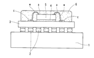
- a package substrate 3 is provided on a wiring board 1 via solder balls 2, and a semiconductor element is further provided on the package substrate 3 via a die bonding material 4.
- a (chip) 5 is provided and the semiconductor element 5 is sealed with a sealing material 6.
- the electrical connection between the electrode a of the semiconductor element 5 and the conductor wiring (terminal) c of the package substrate 3 in this semiconductor package is performed by the ball bonding method.
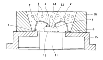
- the LED 13 is provided on the case heat sink 11 via the die bonding material 12 and the phosphor e is mixed.
- the LED 13 is sealed with the material 14.
- the electrical connection between the electrode a of the LED 13 and the conductor wiring (terminal) c of the case electrode 15 in this package is performed by the ball bonding method as in the case of a semiconductor package such as BGA.
- 16 is a resin case body.
- connection methods by these ball bonding methods are generally in the form shown in FIGS. 3A to 3H.
- the wire W shown in FIG. 3A is inserted into the capillary 10a and a ball ( From the state where FAB: Free Air Ball) b is formed, the clamp 10b is opened and the capillary 10a is lowered toward the electrode a on the integrated circuit element. At this time, the ball (FAB) b is captured in the capillary 10a.
- the capillary 10a grips the molten ball b and applies heat / load / ultrasonic waves to the molten ball b, whereby the molten ball b Is bonded to the electrode a by solid phase bonding to form a 1st bond and bonded to the electrode a (1st bonding, FIG. 3B).
- the capillary 10a moves up to a certain height (FIG. (C)) and then moves to a position directly above the conductor wiring c (FIGs. (D) to (e)).
- a special movement is performed on the capillary 10a so that the wire W is attached with a “string” (see the solid line from the chain line in FIG. 4D).
- Capillary 10a that reaches directly above the conductor wiring c descends toward the conductor wiring c and presses the wire W against the conductor wiring (2nd target) c ((e) to (f) in the figure). At the same time, heat, a load, and an ultrasonic wave are applied to the pressed portion, thereby deforming the wire W and joining the wire W onto the conductor wiring c, and a tail that secures the tail in the next step. A bond is formed (2nd junction, FIG. 5F).
- the capillary 10a rises with the wire W remaining, and after securing a tail of a certain length at the tip of the capillary 10a, the clamp 10b is closed (by grabbing the wire W), and the tail The wire W is torn off from the bond portion ((g) in the figure).
- the capillary 10a stops when it rises to the required height, and the tip of the wire W secured at the tip of the capillary 10a is discharged (sparked) by applying a high voltage with the discharge rod g, and the wire is heated by the heat. W is melted, and the melted wire material is turned into a spherical ball b by the surface tension to be hardened ((h) in the figure).
- the bonding wire (wire) W used in this ball bonding method gold of 4N (purity: 99.99 mass% or more) to 2N is used. As described above, gold is frequently used because the shape of the gold ball b is a perfect sphere and the hardness of the gold ball b to be formed is appropriate, and the chip 5 is damaged by the load and ultrasonic wave during bonding. This is because reliable bonding is possible and the reliability is high. On the other hand, in a semiconductor package such as a BGA, since the gold bonding wire W is expensive, it is replaced with an inexpensive copper (Cu) bonding wire.
- Cu copper
- JP 2007-123597 A JP-A-57-194232 Japanese Patent Laid-Open No. 58-6948 JP-A-11-288896
- Gold bonding wires are expensive.
- the copper bonding wire that is an alternative material is inexpensive, but the FAB is harder than the gold bonding wire, and if the tip of the electrode a is fragile, the risk of chip damage increases.
- the 2nd bondability is poor as compared with the gold bonding wire, and there is a problem in the continuous bonding property.
- the Pd surface-coated copper bonding wire has better 2nd bondability and better continuous bondability than the copper bonding wire, but the FAB is harder than the copper bonding wire, which causes a problem of chip damage.
- an Al alloy (Al-Si-Cu etc.) pad has been used for the electrode a of a semiconductor package such as a BGA.
- a semiconductor package such as a BGA.
- it is required to have high temperature reliability, for example, reliability at 150 ° C. or higher.
- Ni / Pd / Au nickel / palladium / gold.
- it is necessary to reduce damage to the fragile chip 5.
- the Pd surface-coated copper bonding wire is difficult to bond to the Ni / Pd / Au coated electrode a, and the copper bonding wire should be bonded under conditions that do not damage the fragile chip 5. Then, there is a problem that sufficient joining cannot be performed.
- the LED 13 of the electrode a coated with Au is used, and a gold bonding wire is used for connection with the electrode a. Since the cost cannot be reduced with this combination using gold, an inexpensive bonding wire is also desired for the LED 13.
- the copper bonding wire has difficulty in continuous bonding, and the Pd surface-coated copper bonding wire has a hard FAB, which may cause chip damage.
- the bonding wire itself has a low reflectance, the wire portion becomes a shadow, so the brightness of the LED 13 itself may be lowered depending on the type of the LED 13.
- Patent Document 4 in order to improve wire strength and heat resistance, Ca (calcium), Sr (strontium), Y (yttrium), La (lanthanum), Ce (cerium), Eu (europium), Be ( It is described that elements such as beryllium), Ge (germanium), In (indium), and Sn (tin) are added. However, when these elements are added in a large amount, the hardness of the ball b increases and the electrode a Have problems to damage.
- Pt platinum
- Pd platinum
- Cu Ru (ruthenium), Os (osmium), Rh (rhodium), Ir (iridium), and Au are added in order to increase the bonding reliability of the wire. It is described.
- the electric resistance of the wire itself is increased, resulting in a problem that the performance as the bonding wire W is impaired. That is, as described above, in a semiconductor package such as a BGA, the electrodes a are smaller and the distance between the electrodes a is closer, so that it is required to reduce the first junction. For this purpose, it is necessary to reduce the diameter of the bonding wire. However, if the electric resistance of the wire increases, there is a problem that the diameter of the wire cannot be reduced. In the LED 13, the operating current is increased to increase the luminance. However, if the electric resistance of the wire is high, a problem of heat generation occurs and a problem of shortening the life of the sealing resin occurs.
- the present invention has an object to provide a bonding wire that has good bonding properties with Ni / Pd / Au coated electrode a or Au coated electrode a, has excellent thermal shock resistance, and is cheaper than a gold bonding wire.
- the present invention provides a bonding wire for connecting a Ni / Pd / Au coated electrode of a semiconductor element or an Au coated electrode and a conductor wiring of a circuit wiring board by a ball bonding method.
- the balance is made of Ag and inevitable impurities, and the tensile strength at normal temperature of the wire (W) is 18 kgf / mm 2 or more and 32 kgf / mm 2 or less, preferably 18 kgf / mm 2 or more and 25 kgf / mm 2 or less.
- the tensile strength at high temperature tensile test of performing a tensile test at °C oven is 14 kgf / mm 2 or more, more preferably 15 kgf / mm 2 or more It was.
- the high-temperature tensile test in the 250 ° C. furnace is preferably performed at 250 ° C. as it is after heating the wire at 250 ° C. for 20 seconds.
- the bonding wire mainly composed of Ag can be made cheaper than the bonding wire mainly composed of Au.
- the bonding wire mainly composed of Ag has high corrosion resistance at the joint portion with the Ni / Pd / Au coated electrode or Au coated electrode, but the joint portion with the Al electrode has low corrosion resistance.
- One or more elements selected from Pd and Au are added in order to obtain corrosion resistance and good electrical characteristics. If at least one element selected from Pd and Au is less than 1.0% by mass, the resistance to sulfidation of the wire may become a problem, and a substance that promotes sulfidation in the atmosphere or in the sealing resin (sulfurization) When hydrogen or the like is present, silver sulfide is generated on the surface of the wire, thereby reducing the reliability of the connection portion. On the other hand, if an amount exceeding 4.0% by mass is added, the electric resistance of the wire becomes too high, and it becomes difficult to reduce the diameter of the wire.
- One or more elements selected from Ca and rare earth elements are added in order to improve wire strength and heat resistance.
- the content is less than 20 ppm by mass, the heat resistance of the wire is lowered and there is a practical problem. Arise.
- bowl b will become high and the electrode a will be damaged at the time of 1st joining. Therefore, the total addition amount of at least one element selected from Ca and rare earth elements is 20 mass ppm or more and 500 mass ppm or less.
- the heat resistance of a wire is high and the damage degree of the electrode a at the time of 1st joining can also be restrained lower.
- addition of Ca is most preferable.
- the wire diameter of the wire W is arbitrary as long as it can be used as a bonding wire, and is, for example, 12 ⁇ m or more and 50.8 ⁇ m or less. If it is 50.8 ⁇ m or less, the molten ball b can be made smaller, and if it is less than 12 ⁇ m, it becomes difficult for an operator to pass the wire W through the capillary 10a before bonding, workability is deteriorated, and air pressure is applied to the wire by air pressure. Sufficient tension cannot be applied, and loop control may be difficult.
- Various methods can be used for manufacturing the above-described bonding wire W.
- 1.0 to 4.0 mass of one or more elements selected from Pd and Au are added to Ag having a purity of 99.99 mass% or more.
- %, Ca, and one or more elements selected from rare earths are added in a total of 20 to 500 ppm by mass, and a rod having the chemical composition with a large wire diameter is produced by a continuous casting method, and the wire diameter is reduced to 50.8 ⁇ m or less.
- the wire is drawn to a predetermined wire diameter. Thereafter, the wire W is subjected to a tempering heat treatment.
- the tempering heat treatment is a continuous heat treatment by drawing the wire W to a predetermined wire diameter and winding the wire W around the reel, running it in a tubular heat treatment furnace, and winding it again with a take-up reel. .
- N 2 gas or a gas obtained by mixing a small amount of hydrogen with N 2 is allowed to flow.
- the furnace temperature is 350 ° C. or more and 600 ° C. or less, and the heat treatment is performed at a wire traveling speed of 30 to 90 m / min. At this time, for example, if the furnace length is 50 cm, the refining heat treatment time is 0.33 to 1 second when the wire traveling speed is 30 to 90 m / min.
- the “room temperature tensile strength” of the bonding wire W is a value obtained by dividing a broken load of the wire W by a cross-sectional area when a sample having a length of 100 mm is subjected to a tensile test at room temperature of 15 to 25 ° C.
- the “high temperature tensile strength” of the bonding wire W is a sample having a length of 100 mm heated in a furnace at 250 ° C. and then subjected to a tensile test in a furnace at 250 ° C., and the broken load of the wire W is divided by the cross-sectional area. Indicates the value.
- the room temperature tensile strength is less than 18 kgf / mm 2 , the wire strength is insufficient, and a wire flow is generated in which the wire loop is deformed by the resin flowing in during resin sealing after wire bonding.
- it exceeds 32 kgf / mm ⁇ 2 > 2nd bondability will worsen and will cause a machine stop. More preferably, if it is 25 kgf / mm 2 or less, 2nd bondability is high, and stable production is possible even at a low temperature setting such as a stage temperature of 150 ° C.
- the high-temperature tensile strength is less than 14 kgf / mm 2 , there is a problem in the life when the product after resin sealing is exposed to a thermal cycle test, but it is more preferably 15 kgf / mm 2 or more. Thermal cycling characteristics are obtained.
- the furnace temperature was set to 350 ° C. or more and 600 ° C. or less, and the wire traveling speed was set to 30 to 90 m / min. This is because the wire W having a chemical composition such as 1.0 to 4.0% by mass could be adjusted so that the normal temperature tensile strength was 18 to 32 kgf / mm 2 and the high temperature tensile strength was 14 kgf / mm 2 or more. .
- the present invention is mainly composed of Ag as described above, it can be made cheaper than bonding wires mainly composed of Au, and can be appropriately added by adding appropriate amounts of Pd, Au, Ca, and rare earth elements. It becomes a wire of sufficient strength and can have good bondability with the Ni / Pd / Au coated electrode or Au electrode.
- a silver alloy having chemical components shown in Table 1 was cast to prepare an 8 mm ⁇ wire rod.
- the wire rod was drawn into a silver alloy wire having a predetermined final wire diameter (12 to 50 ⁇ m ⁇ ), and continuously annealed at various heating temperatures and heating times in a nitrogen atmosphere.
- the tempering heat treatment by the continuous annealing was performed in a furnace having a furnace length of 50 cm at a furnace temperature of 350 ° C. or more and 600 ° C. or less and a wire traveling speed of 30 to 90 m / min.
- the chemical components were quantified by ICP-OES (high frequency inductively coupled plasma emission spectroscopy).
- Each of the continuously annealed wires W was subjected to a tensile test at a room temperature of 15 to 25 ° C. to measure a room temperature tensile strength (kgf / mm 2 ).
- a wire W having a sample length of 100 mm was pulled at a tensile speed of 10 m / min, the breaking load at the time of breaking was measured, and the breaking load / cross-sectional area was calculated.
- the room temperature tensile strength is “room temperature breaking load”.
- the wire W was heated in a furnace at 250 ° C. for 20 seconds, and kept at 250 ° C. as it was, pulled at a rate of 10 m / min. Measured and calculated as the breaking load / cross-sectional area.
- the tensile strength is “high temperature breaking load”.
- Thermal cycle test After bonding, the resin-sealed semiconductor sample was evaluated using a commercially available thermal cycle test apparatus. With respect to the temperature history, a cycle of -40 ° C./30 minutes to 125 ° C./30 minutes was taken as one cycle, and 1000 cycles of tests were conducted. Electrical tests were performed after the test to evaluate continuity. The number of wires evaluated is 500, and when the defect rate is 0, the resistance to the thermal cycle is high, so “A”, when the defect rate is 1% or less, “B”, when it exceeds 1%, it is resistant Is “D” because of low.
- Comparative Example 1 shows that “D” in the sulfidation resistance of the wire exceeds 4.0% by mass. In the evaluation of resistance, it is “D”, and both are “D” in the overall evaluation.
- the total of Pd and Au is 1.0 to 4.0% by mass, and the total of one or more elements selected from Ca, Y, Sm, La, and Ce since but 20 mass ppm or more, including 500 mass ppm or less, and the tensile strength at a tensile test carried out tests with a tensile strength of 18 ⁇ 32kgf / mm 2, 250 °C oven at room temperature is 14 kgf / mm 2 or more, Obtain “A” or “B” in continuous bonding, thermal cycle test, evaluation of chip damage just below the 1st junction, electrical resistance, evaluation of wire flow during resin sealing, and evaluation of sulfidation resistance of wires. In the comprehensive evaluation, “B” or more is obtained, and it is understood that there is no practical problem.
- Examples 1 to 3, 5 to 7, 9, and Comparative Examples 1 to 3 , 6, 7, and 9 are “A” in the evaluation of chip damage immediately below the 1st junction, and it can be understood that the chip has high reliability.
- the tensile strength at normal temperature is 18 to 25 kgf / mm 2
- the tensile strength in a 250 ° C. furnace is 15 kgf / mm 2 or more, from Examples 2, 4, 5, 7, 9, 10, and Comparative Examples 1, 7, 8, 10, A ”.
- one or more elements selected from Pd and Au in total are 1.0 mass% or more and 4.0 mass% or less, and one or more elements selected from Ca and rare earth elements are total 20 mass ppm or more. , 500 ppm by mass or less, the balance being made of Ag and inevitable impurities, the tensile strength of the wire W at room temperature is 18 to 32 kgf / mm 2 , and after heating the wire in a furnace at 250 ° C. for 20 seconds, When the tensile strength in a tensile test conducted in a furnace at 14 ° C.
Landscapes
- Chemical & Material Sciences (AREA)
- Engineering & Computer Science (AREA)
- Materials Engineering (AREA)
- Mechanical Engineering (AREA)
- Metallurgy (AREA)
- Organic Chemistry (AREA)
- Physics & Mathematics (AREA)
- Thermal Sciences (AREA)
- Crystallography & Structural Chemistry (AREA)
- Wire Bonding (AREA)
Abstract
Ni/Pd/Au被覆電極(a)又はAu被覆電極(a)との接合性がよく、耐熱衝撃性に優れ、金ボンディングワイヤより安価なボンディング用ワイヤとする。ボールボンディング法によって接続するためのボンディング用ワイヤ(W)であって、Pd、Auから選ばれる1種以上の元素を合計で1.0質量%以上、4.0質量%以下、Ca、Y、La、Sm、Ceから選ばれる1種以上の元素を合計で20質量ppm以上、500質量ppm以下含み、残部がAgおよび不可避不純物からなり、常温での引張強度が18~32kgf/mm2、250℃炉中での引張強度が14kgf/mm2以上である。この構成であると、連続ボンディング性、熱サイクル試験、1st接合部直下のチップ損傷の評価、電気抵抗、樹脂封止時のワイヤフローの評価、ワイヤの耐硫化性の各評価において、実用上問題ないものとなる。
Description
この発明は、パワーIC、LSI、トランジスタ、BGA(Ball Grid Array package)、QFN(Quad Flat Non lead package)、LED(発光ダイオード)等の半導体パッケージにおける半導体素子上のニッケル・パラジウム・金(Ni/Pd/Au)被覆電極又はAu被覆電極と、リードフレーム、セラミック基板、プリント基板等の回路配線基板の導体配線とをボールボンディング法によって接続するためのボンディング用ワイヤに関するものである。
上記BGA等の半導体パッケージは、例えば、図1に示すように、配線板1上にはんだボール2を介してパッケージ基板3を設け、さらに、そのパッケージ基板3にダイボンディング材4を介して半導体素子(チップ)5を設けて、その半導体素子5を封止材6によって封止した構造である。この半導体パッケージにおける半導体素子5の電極aとパッケージ基板3の導体配線(端子)cとの電気接続は、上記ボールボンディング法によって行われる。
また、上記半導体素子の一つであるLEDのパッケージにおいては、例えば、図2に示すように、ケースヒートシンク11にダイボンディング材12を介してLED13を設けて、蛍光体eを混ぜ合わせた封止材14によってLED13を封止した構造である。このパッケージにおけるLED13の電極aとケース電極15の導体配線(端子)cとの電気接続は、BGA等の半導体パッケージと同様に上記ボールボンディング法によって行われる。図中、16は樹脂製ケースボディである。
これらのボールボンディング法による接続方法は、図3(a)~(h)に示す態様が一般的であり、同図(a)に示す、ワイヤWがキャピラリー10aに挿通されてその先端にボール(FAB:Free Air Ball)bが形成された状態から、クランプ10bが開いて、キャピラリー10aが集積回路素子上の電極aに向かって降下する。このとき、ボール(FAB)bはキャピラリー10a内に捕捉される。
ターゲットである電極aに溶融ボールbが接触すると(キャピラリー10aが電極aに至ると)キャピラリー10aが溶融ボールbをグリップし、溶融ボールbに熱・荷重・超音波を与え、それによって溶融ボールbが圧着されて(圧着ボールb’となって)電極aと固相接合され、1stボンドが形成されて電極aと接着する(1st接合、図3(b))。
1stボンドが形成されれば、キャピラリー10aは、一定高さまで上昇した後(同図(c))、導体配線cの真上まで移動する(同図(d)~(e))。このとき、安定したループを形成するため、キャピラリー10aに特殊な動きをさせてワイヤWに「くせ」を付ける動作をする場合がある(同図(d)の鎖線から実線参照)。
1stボンドが形成されれば、キャピラリー10aは、一定高さまで上昇した後(同図(c))、導体配線cの真上まで移動する(同図(d)~(e))。このとき、安定したループを形成するため、キャピラリー10aに特殊な動きをさせてワイヤWに「くせ」を付ける動作をする場合がある(同図(d)の鎖線から実線参照)。
導体配線cの真上に至ったキャピラリー10aは、導体配線cに向かって降下し、ワイヤWを導体配線(2ndターゲット)cに押付ける(同図(e)~(f))。これと同時に、その押付け部位に熱・荷重・超音波を与え、それによってワイヤWを変形させ、ワイヤWを導体配線c上に接合させるためのステッチボンドと、次のステップでテイルを確保するテイルボンドを形成する(2nd接合、同図(f))。
その両ボンドを形成した後、キャピラリー10aはワイヤWを残したまま上昇し、キャピラリー10aの先端に一定の長さのテイルを確保した後、クランプ10bを閉じて(ワイヤWをつかんで)、テイルボンドの部分からワイヤWを引きちぎる(同図(g))。
キャピラリー10aは、所要の高さまで上昇すると停止し、そのキャピラリー10aの先端に確保されたワイヤWの先端部分に、放電棒gでもって高電圧を掛けて放電し(スパークし)、その熱でワイヤWを溶かし、この溶けたワイヤ素材は表面張力によって球状に近い溶融ボールbになって固まる(同図(h))。
以上の作用で一サイクルが終了し、以後、同様な作用によって、電極aと導体配線cとのボールボンディング法による接続がなされる。
このボールボンディング法に使用されるボンディング線(ワイヤ)Wの材質としては、4N(純度:99.99質量%以上)~2Nの金が使用されている。このように金が多用されるのは金ボールbの形状が真球状となるとともに、形成される金ボールbの硬さが適切であって、接合時の荷重、超音波によってチップ5を損傷することがなく、確実な接合ができ、その信頼性が高いからである。
一方、BGA等の半導体パッケージにおいては、金ボンディングワイヤWは高価であることから、安価な銅(Cu)ボンディングワイヤへの置き換えもなされている。さらに、その銅ボンディングワイヤ表面にパラジウム(Pd)等を被覆することによって、銅ボンディングワイヤで課題となる2nd接合性を高め、生産性を改善したPd表面被覆銅ボンディングワイヤが開発され、一部では使用されている(下記特許文献1)。また、銀(Ag)ボンディングワイヤについても開発され、一部では使用されている。(下記特許文献2、3、4)
一方、BGA等の半導体パッケージにおいては、金ボンディングワイヤWは高価であることから、安価な銅(Cu)ボンディングワイヤへの置き換えもなされている。さらに、その銅ボンディングワイヤ表面にパラジウム(Pd)等を被覆することによって、銅ボンディングワイヤで課題となる2nd接合性を高め、生産性を改善したPd表面被覆銅ボンディングワイヤが開発され、一部では使用されている(下記特許文献1)。また、銀(Ag)ボンディングワイヤについても開発され、一部では使用されている。(下記特許文献2、3、4)
金ボンディングワイヤは高価である。その代替材である銅ボンディングワイヤは安価ではあるが、金ボンディングワイヤに比べてFABが硬く、電極aのチップが脆弱であるとチップダメージ発生の恐れが高くなる。また、金ボンディングワイヤに比べて2nd接合性が悪く、連続ボンディング性に問題がある。
Pd表面被覆銅ボンディングワイヤは、銅ボンディングワイヤに比べて2nd接合性がよく、連続ボンディング性がよいが、FABが銅ボンディングワイヤよりもさらに硬くなるため、チップダメージ発生の問題がある。
Pd表面被覆銅ボンディングワイヤは、銅ボンディングワイヤに比べて2nd接合性がよく、連続ボンディング性がよいが、FABが銅ボンディングワイヤよりもさらに硬くなるため、チップダメージ発生の問題がある。
また、従来、BGA等の半導体パッケージの電極aにはAl合金(Al-Si-Cu等)パッドが用いられていたが、高温信頼性、例えば150℃以上における信頼性が求められる車載などの用途ではNi/Pd/Au(ニッケル/パラジウム/金)被覆した電極aが検討されている。さらに脆弱なチップ5に対するダメージ低減の必要もある。
このNi/Pd/Au被覆電極aに対し、上記Pd表面被覆銅ボンディングワイヤは接合し難いという問題があり、銅ボンディングワイヤは、脆弱なチップ5に対してダメージを与えないような条件でボンディングしようとすると、十分な接合ができないという問題がある。
このNi/Pd/Au被覆電極aに対し、上記Pd表面被覆銅ボンディングワイヤは接合し難いという問題があり、銅ボンディングワイヤは、脆弱なチップ5に対してダメージを与えないような条件でボンディングしようとすると、十分な接合ができないという問題がある。
さらに、従来、LEDパッケージにおいてはAu被覆した電極aのLED13が用いられ、電極aとの接続には金ボンディングワイヤが用いられている。この金を用いた組み合わせではコストダウンができないため、LED13用にも安価なボンディングワイヤが望まれている。しかし、銅ボンディングワイヤは連続ボンディング性に難があり、Pd表面被覆銅ボンディングワイヤではFABが硬くなるため、チップダメージが発生する恐れがある。また、銅ボンディングワイヤ又はPd表面被覆銅ボンディングワイヤを用いると、ボンディングワイヤ自体の反射率が低いため、ワイヤ部分が影になることからLED13の種類によってはLED13そのものの輝度を低下させることもある。
また、従来の銀ボンディングワイヤでは、ボールbを形成する際に窒素(N2)ガスを吹き付けて不活性雰囲気で放電するのが一般的である。これに対し、特許文献2、3に、Ag(銀)にAl(アルミニウム)もしくはMg(マンガン)を添加することにより、N2ガスを吹き付けることなく大気中で放電しても形状のよいボールbを得ることができることが記載されている。
しかし、近年、BGAの半導体パッケージでは、電極aが小さくなり、また、電極a同士の距離も近くなっているので、より安定した真球状のボールbを得る必要があるため、銀ボンディングワイヤにおいても、一般的なN2ガスを吹き付けて放電する方が好ましくなっている。このN2ガスを吹き付けて放電した場合、周囲からの酸素の侵入は防ぐことができるが、ワイヤ先端が溶融した際にワイヤ表面の酸化銀から上記添加したAlもしくはMgが酸素を奪い、Al2O3もしくはMgOができる。このとき、AlもしくはMgを多量に含有していると、このAl2O3もしくはMgOがボールb表面に大量に生成してしまい、電極aとの接合の際に硬質なAl2O3もしくはMgOが電極aを損傷する問題がある。
しかし、近年、BGAの半導体パッケージでは、電極aが小さくなり、また、電極a同士の距離も近くなっているので、より安定した真球状のボールbを得る必要があるため、銀ボンディングワイヤにおいても、一般的なN2ガスを吹き付けて放電する方が好ましくなっている。このN2ガスを吹き付けて放電した場合、周囲からの酸素の侵入は防ぐことができるが、ワイヤ先端が溶融した際にワイヤ表面の酸化銀から上記添加したAlもしくはMgが酸素を奪い、Al2O3もしくはMgOができる。このとき、AlもしくはMgを多量に含有していると、このAl2O3もしくはMgOがボールb表面に大量に生成してしまい、電極aとの接合の際に硬質なAl2O3もしくはMgOが電極aを損傷する問題がある。
同様に、特許文献4にワイヤ強度や耐熱性を向上させるために、Ca(カルシウム)、Sr(ストロンチウム)、Y(イットリウム)、La(ランタン)、Ce(セリウム)、Eu(ユウロピウム)、Be(ベリリウム)、Ge(ゲルマニウム)、In(インジウム)、Sn(スズ)等の元素を添加することが記載されているが、これらの元素については多量に添加すると、ボールbの硬度が上がって電極aを損傷する問題がある。
また、特許文献4にはワイヤの接合信頼性を高めるために、Pt(白金)、Pd、Cu、Ru(ルテニウム)、Os(オスミウム)、Rh(ロジウム)、Ir(イリジウム)、Auを添加することが記載されている。しかし、このような元素を多量に添加すれば、ワイヤ自体の電気抵抗が上がり、ボンディングワイヤWとしての性能を損なう問題が生じる。すなわち、上述のとおりBGA等の半導体パッケージでは、電極aはより小さく、その電極a間の距離もより近くなっているため、1st接合部を小さくすることが求められている。そのためには、ボンディングワイヤの直径を小さくする必要があるが、ワイヤの電気抵抗が高くなると、ワイヤの直径を小さくすることができなくなる問題がある。また、LED13においては、輝度を上げるために動作電流が高くなってきているが、ワイヤの電気抵抗が高いと発熱の問題が生じ、封止樹脂の寿命を縮める不具合が生じる。
また、特許文献4にはワイヤの接合信頼性を高めるために、Pt(白金)、Pd、Cu、Ru(ルテニウム)、Os(オスミウム)、Rh(ロジウム)、Ir(イリジウム)、Auを添加することが記載されている。しかし、このような元素を多量に添加すれば、ワイヤ自体の電気抵抗が上がり、ボンディングワイヤWとしての性能を損なう問題が生じる。すなわち、上述のとおりBGA等の半導体パッケージでは、電極aはより小さく、その電極a間の距離もより近くなっているため、1st接合部を小さくすることが求められている。そのためには、ボンディングワイヤの直径を小さくする必要があるが、ワイヤの電気抵抗が高くなると、ワイヤの直径を小さくすることができなくなる問題がある。また、LED13においては、輝度を上げるために動作電流が高くなってきているが、ワイヤの電気抵抗が高いと発熱の問題が生じ、封止樹脂の寿命を縮める不具合が生じる。
さらに、昨今、車載用途を中心にして、半導体パッケージの信頼性評価の基準は厳しくなってきており、特に低温・高温保持を繰り返す耐熱衝撃性についてはその要求が高くなってきたりしている。
上記の銀ワイヤを用いて組み上げた半導体パッケージをより厳しい熱サイクル試験にかけると、基板の反りや樹脂の膨張収縮の影響でワイヤが破断する場合があった。
上記の銀ワイヤを用いて組み上げた半導体パッケージをより厳しい熱サイクル試験にかけると、基板の反りや樹脂の膨張収縮の影響でワイヤが破断する場合があった。
因みに、金ボンディングワイヤとNi/Pd/Au被覆電極a又はAu被覆電極aとの接合であれば、高い耐熱衝撃性は得られるが、材料費が高価になるという問題がある。
この発明は、以上の実状の下、Ni/Pd/Au被覆電極a又はAu被覆電極aとの接合性がよく、耐熱衝撃性に優れ、金ボンディングワイヤより安価なボンディング用ワイヤとすることを課題とする。
上記課題を達成するため、この発明は、半導体素子のNi/Pd/Au被覆電極又はAu被覆電極と回路配線基板の導体配線とをボールボンディング法によって接続するためのボンディング用ワイヤにおいて、Pd、Auから選ばれる1種以上の元素を合計で1.0質量%以上、4.0質量%以下、Ca、希土類元素から選ばれる1種以上の元素を合計で20質量ppm以上、500質量ppm以下含み、残部がAgおよび不可避不純物からなり、そのワイヤ(W)の常温での引張強度が18kgf/mm2以上32kgf/mm2以下、好ましくは18kgf/mm2以上25kgf/mm2以下とし、ワイヤを250℃炉中で引張試験を行う高温引張試験での引張強度が14kgf/mm2以上、より好ましくは15kgf/mm2以上とした。このとき、その250℃炉中の高温引張試験は、ワイヤを250℃で20秒間加熱した後、そのまま250℃で行なうことが好ましい。
Agを主体とするボンディングワイヤは、Auを主体とするボンディングワイヤに比べれば、安価なものとし得る。
因みに、Agを主体とするボンディングワイヤは、Ni/Pd/Au被覆電極又はAu被覆電極との接合箇所の耐食性は高いが、Al電極との接合箇所は耐食性が低い。
因みに、Agを主体とするボンディングワイヤは、Ni/Pd/Au被覆電極又はAu被覆電極との接合箇所の耐食性は高いが、Al電極との接合箇所は耐食性が低い。
Pd、Auから選ばれる1種以上の元素は、耐食性及び良好な電気特性を得るために添加する。Pd、Auから選ばれる1種以上の元素が1.0質量%未満であると、ワイヤの耐硫化性が問題になることがあり、大気中もしくは封止樹脂中に硫化を促進する物質(硫化水素等)が存在すると、ワイヤ表面に硫化銀が生成することで、接続部の信頼性が低下する。
一方、4.0質量%を超えた量を添加すると、ワイヤの電気抵抗が高くなりすぎるため、ワイヤの直径を小さくすることが難しくなる。
一方、4.0質量%を超えた量を添加すると、ワイヤの電気抵抗が高くなりすぎるため、ワイヤの直径を小さくすることが難しくなる。
Ca、希土類元素から選ばれる1種以上の元素は、ワイヤ強度や耐熱性を向上させるために添加するが、20質量ppm未満であると、そのワイヤの耐熱性が低くなって実用上の問題が生じる。また、500質量ppmを超えて添加すると、ボールbの硬度が高くなり、1st接合時に電極aが損傷する。よって、Ca、希土類元素から選ばれる1種以上の元素の合計添加量は20質量ppm以上500質量ppm以下とする。また、より好ましくは20質量ppm以上100質量ppm以下であり、この範囲であれば、ワイヤの耐熱性が高く、1st接合時の電極aの損傷の度合いもより低く抑えることができる。ここで、希土類元素は入手性に難があるため、Caの添加が最も好ましい。
このワイヤWの線径はボンディングワイヤとして使用し得れば任意であるが、例えば、12μm以上50.8μm以下とする。50.8μm以下とすると溶融ボールbをより小さくでき、12μm未満であると、ボンディング前にオペレータがワイヤWをキャピラリー10aに通すのが困難になり、作業性が悪くなるうえに、空気圧によりワイヤに十分な張力をかけることができなくなり、ループ制御が困難になる恐れがある。
上述のボンディングワイヤWの製造方法には種々のものが採用できるが、例えば、純度99.99質量%以上のAgにPd、Auから選ばれる1種以上の元素を1.0~4.0質量%、Ca、希土類から選ばれる1種以上の元素を合計で20~500質量ppm添加し、連続鋳造法で大きな線径のその化学組成のロッドを作製し、線径50.8μm以下までダイスに順次貫通させていくことにより、所定の線径に伸線する。その後、ワイヤWに調質熱処理を施す。
その調質熱処理は、所定の線径まで伸線を行いリールに巻きとられたワイヤWを、巻き戻して管状の熱処理炉中に走行させ、再び巻き取りリールで巻き取ることによって連続熱処理を行う。管状の熱処理炉中にはN2ガスもしくはN2に微量の水素を混合させたガスを流す。また、その炉温度は350℃以上600℃以下として、ワイヤ走行速度は30~90m/分で熱処理を行う。このとき、例えば、炉長:50cmであれば、ワイヤ走行速度:30~90m/分の場合、調質熱処理時間は0.33~1秒となる。
ボンディングワイヤWの「常温引張強度」は、15~25℃の室温中で長さ100mmの試料を引張試験し、ワイヤWの破断した荷重を断面積で除した値を示す。
また、ボンディングワイヤWの「高温引張強度」は長さ100mmの試料を250℃の炉中で加熱し、その後250℃の炉中で引張試験し、ワイヤWの破断した荷重を断面積で除した値を示す。
ここで、常温引張強度が18kgf/mm2未満であるとワイヤ強度が不足して、ワイヤボンディング後の樹脂封止の際に流入してきた樹脂によってワイヤループが変形するワイヤフローが発生する。また、32kgf/mm2を超えると、2nd接合性が悪くなり、マシンストップの原因となる。さらに好ましくは、25kgf/mm2以下であると、2nd接合性が高く、ステージ温度が150℃のような低温設定でも安定した生産が可能になる。
また、高温引張強度が14kgf/mm2未満であると、樹脂封止後の製品を熱サイクル試験に曝した時の寿命に問題が生じるが、より好ましくは15kgf/mm2以上であるとより高い熱サイクル特性が得られる。
また、ボンディングワイヤWの「高温引張強度」は長さ100mmの試料を250℃の炉中で加熱し、その後250℃の炉中で引張試験し、ワイヤWの破断した荷重を断面積で除した値を示す。
ここで、常温引張強度が18kgf/mm2未満であるとワイヤ強度が不足して、ワイヤボンディング後の樹脂封止の際に流入してきた樹脂によってワイヤループが変形するワイヤフローが発生する。また、32kgf/mm2を超えると、2nd接合性が悪くなり、マシンストップの原因となる。さらに好ましくは、25kgf/mm2以下であると、2nd接合性が高く、ステージ温度が150℃のような低温設定でも安定した生産が可能になる。
また、高温引張強度が14kgf/mm2未満であると、樹脂封止後の製品を熱サイクル試験に曝した時の寿命に問題が生じるが、より好ましくは15kgf/mm2以上であるとより高い熱サイクル特性が得られる。
なお、調質熱処理において、炉温度を350℃以上600℃以下、ワイヤ走行速度を30~90m/分としたのは、その熱処理温度とワイヤ走行速度の範囲内であると、上記Pd、Au:1.0~4.0質量%等の化学組成のワイヤWにおいて、常温引張強度が18~32kgf/mm2、高温引張強度が14kgf/mm2以上となるように調整することができたからである。
この発明は、以上のようにAgを主体としたので、Auを主体としたボンディングワイヤに比べれば、安価なものとし得て、かつ、Pd、Au、Ca、希土類元素の適量の添加によって、適度な強度のワイヤとなってNi/Pd/Au被覆電極又はAu電極との接合性が良いものとすることができる。
純度が99.99質量%以上(4N)の高純度Agを用いて、表1に示す化学成分の銀合金を鋳造し、8mmφのワイヤロッドを作成した。そのワイヤロッドを伸線加工し所定の最終線径(12~50μmφ)の銀合金線とし、窒素雰囲気中で種々の加熱温度・加熱時間にて連続焼鈍した。その連続焼鈍による調質熱処理は、炉長:50cmの炉において、その炉温度を350℃以上600℃以下、ワイヤ走行速度を30~90m/分で行なった。なお、化学成分の定量はICP-OES(高周波誘導結合プラズマ発光分光分析法)により行った。
その連続焼鈍した各ワイヤWを15~25℃の常温で引張試験を行なって常温引張強度(kgf/mm2)を測定した。その引張試験は試料長さ:100mmのワイヤWを引張速度10m/分の速度で引張り、破断に至る時の破断荷重を測定し、その破断荷重/断面積として算出した。表1においては、その常温引張強度を「常温破断荷重」としている。
また、250℃での引張強度についてはワイヤWを250℃の炉中で20秒間加熱し、そのまま250℃に保持した状態で引張速度10m/分の速度で引張り、破断に至る時の破断荷重を測定し、その破断荷重/断面積として算出した。表1においては、その引張強度を「高温破断荷重」としている。
また、250℃での引張強度についてはワイヤWを250℃の炉中で20秒間加熱し、そのまま250℃に保持した状態で引張速度10m/分の速度で引張り、破断に至る時の破断荷重を測定し、その破断荷重/断面積として算出した。表1においては、その引張強度を「高温破断荷重」としている。

この各実施例及び各比較例に対し、それぞれ下記の試験を行った。
『評価項目』
各ワイヤWについて、自動ワイヤボンダで、図3に示すボールボンディング法による接続を行った。すなわち、放電棒gによるアーク放電によりワイヤW先端にFAB(ボールb)を作製し、それを半導体素子(チップ)5、13上のNi/Pd/Au被覆電極a又はAu被覆電極aに接合し、ワイヤ他端をリード端子(導体配線)cに接合した(図1、図2参照)。なお、FAB作製時にはワイヤW先端部に窒素(N2)ガスを流しながらアーク放電を行った。リード端子cにはAg被覆42%Ni-Fe合金を使用した。
評価に用いたボンディング試料における連続ボンディング性、熱サイクル試験、1st接合部のチップ損傷、電気抵抗、樹脂封止時のワイヤフロー、ワイヤの耐硫化性及び総合評価を表2に示す。それらの評価方法等は以下の通りである。
『評価項目』
各ワイヤWについて、自動ワイヤボンダで、図3に示すボールボンディング法による接続を行った。すなわち、放電棒gによるアーク放電によりワイヤW先端にFAB(ボールb)を作製し、それを半導体素子(チップ)5、13上のNi/Pd/Au被覆電極a又はAu被覆電極aに接合し、ワイヤ他端をリード端子(導体配線)cに接合した(図1、図2参照)。なお、FAB作製時にはワイヤW先端部に窒素(N2)ガスを流しながらアーク放電を行った。リード端子cにはAg被覆42%Ni-Fe合金を使用した。
評価に用いたボンディング試料における連続ボンディング性、熱サイクル試験、1st接合部のチップ損傷、電気抵抗、樹脂封止時のワイヤフロー、ワイヤの耐硫化性及び総合評価を表2に示す。それらの評価方法等は以下の通りである。
『評価方法』
(1)「連続ボンディング性」
ボンディングマシンで10,000回の連続ボンディングを行い、マシンストップが発生しなければ「A」、1回のマシンストップが発生すれば「B」、2回以上のマシンストップが起これば「D」とした。このとき、ステージ温度が低くなれば、その連続ボンディングが困難になることから、175℃(±5℃)、150℃(±5℃)の2水準で行った。
(1)「連続ボンディング性」
ボンディングマシンで10,000回の連続ボンディングを行い、マシンストップが発生しなければ「A」、1回のマシンストップが発生すれば「B」、2回以上のマシンストップが起これば「D」とした。このとき、ステージ温度が低くなれば、その連続ボンディングが困難になることから、175℃(±5℃)、150℃(±5℃)の2水準で行った。
(2)「熱サイクル試験」
ボンディングを行った後、樹脂封止をした半導体試料を市販の熱サイクル試験装置を用いて評価した。温度履歴は-40℃/30分~125℃/30分を1サイクルとして、1000サイクルの試験を行った。試験後に電気的測定を行い、導通評価をした。評価したワイヤ数は500本であり、不良率が0の場合は熱サイクルへの耐性が高いことから「A」、不良率が1%以下の場合は「B」、1%を超える場合は耐性が低いことから「D」とした。
ボンディングを行った後、樹脂封止をした半導体試料を市販の熱サイクル試験装置を用いて評価した。温度履歴は-40℃/30分~125℃/30分を1サイクルとして、1000サイクルの試験を行った。試験後に電気的測定を行い、導通評価をした。評価したワイヤ数は500本であり、不良率が0の場合は熱サイクルへの耐性が高いことから「A」、不良率が1%以下の場合は「B」、1%を超える場合は耐性が低いことから「D」とした。
(3)「ボンディング後、1st接合部直下のチップ損傷の評価」
1st接合部および電極膜を王水で溶解し、半導体素子5、13のクラックを光学顕微鏡と走査型電子顕微鏡(SEM)で観察した。100個の接合部を観察して3μm未満の微小なピットが1個もしくはまったく見られない場合は「A」、3μm以上のクラックが2個以上5個未満認められた場合は使用上問題はないと考えて「B」、3μm以上のクラックが5個以上認められた場合は「D」とした。
1st接合部および電極膜を王水で溶解し、半導体素子5、13のクラックを光学顕微鏡と走査型電子顕微鏡(SEM)で観察した。100個の接合部を観察して3μm未満の微小なピットが1個もしくはまったく見られない場合は「A」、3μm以上のクラックが2個以上5個未満認められた場合は使用上問題はないと考えて「B」、3μm以上のクラックが5個以上認められた場合は「D」とした。
(4)「電気抵抗」
4端子法を用いて室温での電気抵抗を測定した。3試料の固有抵抗の平均が4.0μΩ・cm以下であれば「A」、4.0μΩ・cmを超えれば「D」とした。
4端子法を用いて室温での電気抵抗を測定した。3試料の固有抵抗の平均が4.0μΩ・cm以下であれば「A」、4.0μΩ・cmを超えれば「D」とした。
(5)「樹脂封止時のワイヤフローの評価」
ワイヤ長:5mmのボンディング試料をエポキシ樹脂で封止した後で、X線非破壊観察装置にて最大ワイヤフロー量を測定した。測定は20本行い、その平均値をワイヤ長5mmで除した割合をワイヤフロー率とした。このワイヤフロー率が7%未満なら「A」、7%以上では実用上の問題があると考えて評価を「D」とした。
ワイヤ長:5mmのボンディング試料をエポキシ樹脂で封止した後で、X線非破壊観察装置にて最大ワイヤフロー量を測定した。測定は20本行い、その平均値をワイヤ長5mmで除した割合をワイヤフロー率とした。このワイヤフロー率が7%未満なら「A」、7%以上では実用上の問題があると考えて評価を「D」とした。
(6)「ワイヤの耐硫化性」
容器中で5%硫化アンモニウム溶液を60℃に加熱し、気化させた環境下にワイヤサンプルを放置し、5分間経過後の表面分析をオージェ分光分析法(AES)で測定した。オージェ分光分析法はArイオンで深さ方向に単位時間のスパッタを行い、その都度硫黄濃度を測定していき、最外層の硫黄濃度の1/2の濃度になったところまでを硫化層の厚みとした。厚さの換算には一般的なSiO2換算を用いた。ここで、硫化層の厚みが200Å以下なら「A」、200Åを超えると実用上の問題があると考えて評価を「D」とした。
容器中で5%硫化アンモニウム溶液を60℃に加熱し、気化させた環境下にワイヤサンプルを放置し、5分間経過後の表面分析をオージェ分光分析法(AES)で測定した。オージェ分光分析法はArイオンで深さ方向に単位時間のスパッタを行い、その都度硫黄濃度を測定していき、最外層の硫黄濃度の1/2の濃度になったところまでを硫化層の厚みとした。厚さの換算には一般的なSiO2換算を用いた。ここで、硫化層の厚みが200Å以下なら「A」、200Åを超えると実用上の問題があると考えて評価を「D」とした。
「総合評価」
各評価において、すべてが「A」であるものを「A」、「A」と「B」が混在するものを「B」、一つでも「D」があるものは「D」とした。
各評価において、すべてが「A」であるものを「A」、「A」と「B」が混在するものを「B」、一つでも「D」があるものは「D」とした。
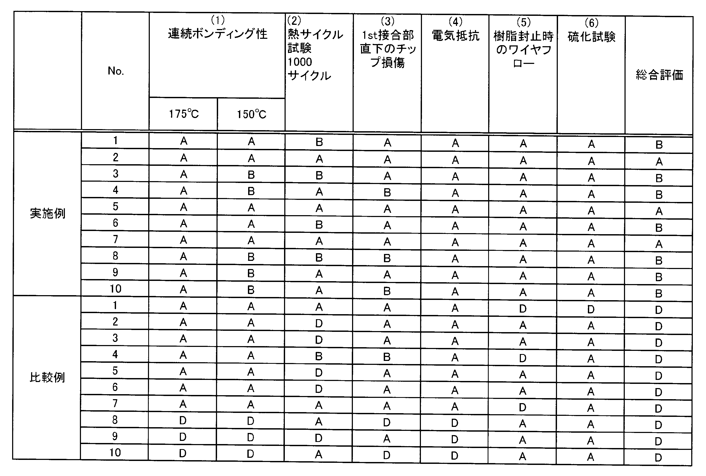
この表1、2において、Ca、Y、Sm、La、Ceから選ばれる1種以上の元素の合計が500質量ppmを超えると、比較例8、10からFAB表面に析出物の生成が確認され、1st接合部のチップ損傷が発生するために「1st接合部のチップ損傷」が「D」となり、総合評価でも「D」となっている。一方、これらの元素合計が20質量%ppm未満であると、比較例5、6、9から、耐熱性が低くなり、熱サイクル試験で「D」となって総合評価で「D」となっている。
また、Pd、Auの合計が1.0質量%未満であると、比較例1から、ワイヤの耐硫化性において「D」、4.0質量%を超えると、比較例8~10から、電気抵抗の評価において「D」となって、共に、総合評価で「D」となっている。
さらに、常温での引張強度(常温破断荷重)が18kgf/mm2未満であると、比較例1、4、7から、樹脂封止時のワイヤフローの評価において「D」となって総合評価で「D」となっている。一方、32kgf/mm2を超えると、比較例8~10から、2nd接合性が悪化するため、連続ボンディング性が「D」となって総合評価で「D」となっている。
また、250℃炉中で試験を行う引張試験での引張強度(高温破断荷重)が14kgf/mm2未満であると、比較例2、3、5、6、9から、熱サイクルへの耐性が低く、熱サイクル試験で「D」となって総合評価で「D」となっている。
また、250℃炉中で試験を行う引張試験での引張強度(高温破断荷重)が14kgf/mm2未満であると、比較例2、3、5、6、9から、熱サイクルへの耐性が低く、熱サイクル試験で「D」となって総合評価で「D」となっている。
これに対し、各実施例1~10は、いずれも、Pd、Auの合計が1.0~4.0質量%、Ca、Y、Sm、La、Ceから選ばれる1種以上の元素の合計が20質量ppm以上、500質量ppm以下含み、常温での引張強度が18~32kgf/mm2、250℃炉中で試験を行う引張試験での引張強度が14kgf/mm2以上であることから、連続ボンディング性、熱サイクル試験、1st接合部直下のチップ損傷の評価、電気抵抗、樹脂封止時のワイヤフローの評価、ワイヤの耐硫化性の各評価において、「A」又は「B」を得ており、総合評価においては、「B」以上を得て、実用上問題ないことがわかる。
また、Ca、Y、Sm、La、Ceから選ばれる1種以上の元素を含み、その合計が100質量ppm以下であれば、実施例1~3、5~7、9、比較例1~3、6、7、9から、1st接合部直下のチップ損傷の評価において「A」となり、高い信頼性を有することが理解できる。さらに、常温での引張強度が18~25kgf/mm2であると、実施例1、2、5~7、比較例2、3、5、6から、150℃における連続ボンディング性評価において「A」となり、低いステージ温度での良好な作業性を得られることが理解できる。また、250℃炉中での引張強度が15kgf/mm2以上であると、実施例2、4、5、7、9、10、比較例1、7、8、10から、熱サイクル試験において「A」となっている。
以上から、Pd、Auから選ばれる1種以上の元素を合計で1.0質量%以上、4.0質量%以下、Ca、希土類元素から選ばれる1種以上の元素を合計で20質量ppm以上、500質量ppm以下含み、残部がAgおよび不可避不純物からなり、ワイヤWの常温での引張強度が18~32kgf/mm2であり、ワイヤを250℃の炉中で20秒間加熱した後、そのまま250℃炉中で試験を行う引張試験での引張強度が14kgf/mm2以上であると、連続ボンディング性、熱サイクル試験、1st接合部直下のチップ損傷の評価、電気抵抗、樹脂封止時のワイヤフローの評価、ワイヤの耐硫化性の各評価において、実用上問題ないものとなり、また、そのCa、希土類元素から選ばれる1種以上の元素の含有量が20質量ppm以上、100質量ppm以下であると、1st接合部直下のチップ損傷の評価において「A」となって高い信頼性を有するものとなり、常温での引張強度が18~25kgf/mm2であると、150℃における連続ボンディング性評価において「A」となり、良好な作業性を得られるものとなり、さらに、250℃炉中での引張強度が15kgf/mm2以上であると、熱サイクルへの耐性が高いものとなる。
3、15 回路配線基板
5 半導体素子
13 LED
W ボンディング用ワイヤ
a 半導体素子(LED)の電極
b 溶融ボール
b’ 圧着ボール
c 回路配線基板の導体配線(リード端子)
5 半導体素子
13 LED
W ボンディング用ワイヤ
a 半導体素子(LED)の電極
b 溶融ボール
b’ 圧着ボール
c 回路配線基板の導体配線(リード端子)
Claims (4)
- 半導体素子(5、13)のNi/Pd/Au被覆電極(a)又はAu被覆電極(a)と回路配線基板(3、15)の導体配線(c)とをボールボンディング法によって接続するためのボンディング用ワイヤ(W)であって、
Pd、Auから選ばれる1種以上の元素を合計で1.0質量%以上、4.0質量%以下、Ca、希土類元素から選ばれる1種以上の元素を合計で20質量ppm以上、500質量ppm以下含み、
残部がAgおよび不可避不純物からなり、
そのワイヤ(W)の常温での引張強度が18~32kgf/mm2であり、ワイヤを250℃の炉中で加熱した後、そのまま250℃炉中で試験を行う引張試験での引張強度が14kgf/mm2以上であることを特徴とするボンディング用ワイヤ。 - 上記ワイヤ(W)のCa、希土類元素から選ばれる1種以上の元素の含有量が20質量ppm以上、100質量ppm以下である請求項1に記載のボンディング用ワイヤ。
- 上記ワイヤ(W)の常温での引張強度が18~25kgf/mm2である請求項1または2に記載のボンディング用ワイヤ。
- 上記ワイヤ(W)の250℃炉中での引張強度が15kgf/mm2以上である請求項1~3のいずれか1項に記載のボンディング用ワイヤ。
Priority Applications (1)
| Application Number | Priority Date | Filing Date | Title |
|---|---|---|---|
| KR1020157014935A KR101905942B1 (ko) | 2012-11-07 | 2013-11-06 | 본딩용 와이어 |
Applications Claiming Priority (2)
| Application Number | Priority Date | Filing Date | Title |
|---|---|---|---|
| JP2012245424A JP5671512B2 (ja) | 2012-11-07 | 2012-11-07 | ボンディング用ワイヤ |
| JP2012-245424 | 2012-11-07 |
Publications (1)
| Publication Number | Publication Date |
|---|---|
| WO2014073555A1 true WO2014073555A1 (ja) | 2014-05-15 |
Family
ID=50684657
Family Applications (1)
| Application Number | Title | Priority Date | Filing Date |
|---|---|---|---|
| PCT/JP2013/079980 Ceased WO2014073555A1 (ja) | 2012-11-07 | 2013-11-06 | ボンディング用ワイヤ |
Country Status (3)
| Country | Link |
|---|---|
| JP (1) | JP5671512B2 (ja) |
| KR (1) | KR101905942B1 (ja) |
| WO (1) | WO2014073555A1 (ja) |
Cited By (5)
| Publication number | Priority date | Publication date | Assignee | Title |
|---|---|---|---|---|
| CN104593634A (zh) * | 2014-12-31 | 2015-05-06 | 北京达博有色金属焊料有限责任公司 | 一种化学镀金钯键合银合金丝及其制备方法 |
| CN109182826A (zh) * | 2018-09-18 | 2019-01-11 | 重庆材料研究院有限公司 | 一种高强韧性、低电阻率的银金合金键合丝 |
| CN109983544A (zh) * | 2017-03-23 | 2019-07-05 | 积水化学工业株式会社 | 导电性粒子、导电材料以及连接结构体 |
| CN110699569A (zh) * | 2019-09-18 | 2020-01-17 | 广东佳博电子科技有限公司 | 一种晶粒分布稳固的键合银丝材料及其制备方法 |
| JP2025092437A (ja) * | 2023-12-07 | 2025-06-19 | 中国机械総院集団鄭州机械研究所有限公司 | ボンディングワイヤー、その調製方法およびledデバイス |
Families Citing this family (3)
| Publication number | Priority date | Publication date | Assignee | Title |
|---|---|---|---|---|
| JP6343197B2 (ja) * | 2014-07-16 | 2018-06-13 | タツタ電線株式会社 | ボンディング用ワイヤ |
| MY179434A (en) | 2016-03-11 | 2020-11-06 | Tatsuta Electric Wire & Cable Co Ltd | Bonding wire |
| JP7761766B2 (ja) * | 2022-07-14 | 2025-10-28 | 田中電子工業株式会社 | 発光ダイオード(led)用ボンディングワイヤ及びled用ボンディングワイヤの製造方法 |
Citations (5)
| Publication number | Priority date | Publication date | Assignee | Title |
|---|---|---|---|---|
| JP2003059964A (ja) * | 2001-08-10 | 2003-02-28 | Tanaka Electronics Ind Co Ltd | ボンディングワイヤ及びその製造方法 |
| JP2012151350A (ja) * | 2011-01-20 | 2012-08-09 | Tatsuta Electric Wire & Cable Co Ltd | ボールボンディング用ワイヤ |
| JP2012182205A (ja) * | 2011-02-28 | 2012-09-20 | Tatsuta Electric Wire & Cable Co Ltd | ボンディングワイヤ及びその製造方法 |
| JP2013048169A (ja) * | 2011-08-29 | 2013-03-07 | Tatsuta Electric Wire & Cable Co Ltd | ボールボンディング用ワイヤ |
| JP2013135042A (ja) * | 2011-12-26 | 2013-07-08 | Tatsuta Electric Wire & Cable Co Ltd | ボールボンディング用ワイヤ |
Family Cites Families (2)
| Publication number | Priority date | Publication date | Assignee | Title |
|---|---|---|---|---|
| JPH11288962A (ja) * | 1998-04-01 | 1999-10-19 | Sumitomo Metal Mining Co Ltd | ボンディングワイヤ |
| DE19821395C2 (de) * | 1998-05-13 | 2000-06-29 | Heraeus Gmbh W C | Verwendung eines Feinstdrahtes aus einer nickelhaltigen Gold-Legierung |
-
2012
- 2012-11-07 JP JP2012245424A patent/JP5671512B2/ja active Active
-
2013
- 2013-11-06 WO PCT/JP2013/079980 patent/WO2014073555A1/ja not_active Ceased
- 2013-11-06 KR KR1020157014935A patent/KR101905942B1/ko active Active
Patent Citations (5)
| Publication number | Priority date | Publication date | Assignee | Title |
|---|---|---|---|---|
| JP2003059964A (ja) * | 2001-08-10 | 2003-02-28 | Tanaka Electronics Ind Co Ltd | ボンディングワイヤ及びその製造方法 |
| JP2012151350A (ja) * | 2011-01-20 | 2012-08-09 | Tatsuta Electric Wire & Cable Co Ltd | ボールボンディング用ワイヤ |
| JP2012182205A (ja) * | 2011-02-28 | 2012-09-20 | Tatsuta Electric Wire & Cable Co Ltd | ボンディングワイヤ及びその製造方法 |
| JP2013048169A (ja) * | 2011-08-29 | 2013-03-07 | Tatsuta Electric Wire & Cable Co Ltd | ボールボンディング用ワイヤ |
| JP2013135042A (ja) * | 2011-12-26 | 2013-07-08 | Tatsuta Electric Wire & Cable Co Ltd | ボールボンディング用ワイヤ |
Cited By (6)
| Publication number | Priority date | Publication date | Assignee | Title |
|---|---|---|---|---|
| CN104593634A (zh) * | 2014-12-31 | 2015-05-06 | 北京达博有色金属焊料有限责任公司 | 一种化学镀金钯键合银合金丝及其制备方法 |
| CN109983544A (zh) * | 2017-03-23 | 2019-07-05 | 积水化学工业株式会社 | 导电性粒子、导电材料以及连接结构体 |
| CN109182826A (zh) * | 2018-09-18 | 2019-01-11 | 重庆材料研究院有限公司 | 一种高强韧性、低电阻率的银金合金键合丝 |
| CN110699569A (zh) * | 2019-09-18 | 2020-01-17 | 广东佳博电子科技有限公司 | 一种晶粒分布稳固的键合银丝材料及其制备方法 |
| JP2025092437A (ja) * | 2023-12-07 | 2025-06-19 | 中国机械総院集団鄭州机械研究所有限公司 | ボンディングワイヤー、その調製方法およびledデバイス |
| JP7774697B2 (ja) | 2023-12-07 | 2025-11-21 | 中国机械総院集団鄭州机械研究所有限公司 | ボンディングワイヤー、その調製方法およびledデバイス |
Also Published As
| Publication number | Publication date |
|---|---|
| JP5671512B2 (ja) | 2015-02-18 |
| KR20150082518A (ko) | 2015-07-15 |
| KR101905942B1 (ko) | 2018-10-08 |
| JP2014096403A (ja) | 2014-05-22 |
Similar Documents
| Publication | Publication Date | Title |
|---|---|---|
| KR101536554B1 (ko) | 본딩용 와이어 | |
| JP5671512B2 (ja) | ボンディング用ワイヤ | |
| CN103155130B (zh) | Ag-Au-Pd三元合金接合线 | |
| KR101707244B1 (ko) | 반도체용 본딩 와이어 | |
| Uno | Bond reliability under humid environment for coated copper wire and bare copper wire | |
| JP5064577B2 (ja) | ボールボンディング用ワイヤ | |
| WO2013018238A1 (ja) | ボールボンディングワイヤ | |
| JP2010199528A (ja) | ボンディングワイヤ | |
| TW202020235A (zh) | 鈀被覆銅接合線及其製造方法 | |
| JP7542583B2 (ja) | ボンディングワイヤ及び半導体装置 | |
| JP6343197B2 (ja) | ボンディング用ワイヤ | |
| JP6103806B2 (ja) | ボールボンディング用ワイヤ | |
| JP5996853B2 (ja) | ボールボンディング用ワイヤ | |
| JP4726206B2 (ja) | 高い初期接合性、高い接合信頼性、圧着ボールの高い真円性、高い直進性、高い耐樹脂流れ性および低い比抵抗を有するボンディングワイヤ用金合金線 | |
| CN111656501B (zh) | 接合线 | |
| Cao et al. | Effect of Ag-4Pd alloy bonding wire properties and structure on bond strengths and reliability | |
| JP6714150B2 (ja) | ボンディングワイヤ及び半導体装置 | |
| JP2013042105A (ja) | ボンディングワイヤ | |
| JP2016072261A (ja) | 銀金合金ボンディングワイヤ | |
| JP2011155129A (ja) | 高温半導体装置用金合金ボンディングワイヤ | |
| WO2006134824A1 (ja) | 高い初期接合性、高い接合信頼性、圧着ボールの高い真円性、高い直進性および高い耐樹脂流れ性を有するボンディングワイヤ用金合金線 | |
| JP2012109556A (ja) | バンプ用ワイヤ |
Legal Events
| Date | Code | Title | Description |
|---|---|---|---|
| 121 | Ep: the epo has been informed by wipo that ep was designated in this application |
Ref document number: 13853212 Country of ref document: EP Kind code of ref document: A1 |
|
| NENP | Non-entry into the national phase |
Ref country code: DE |
|
| ENP | Entry into the national phase |
Ref document number: 20157014935 Country of ref document: KR Kind code of ref document: A |
|
| 122 | Ep: pct application non-entry in european phase |
Ref document number: 13853212 Country of ref document: EP Kind code of ref document: A1 |