WO2014073486A1 - アクティブマトリクス基板、及び表示装置 - Google Patents
アクティブマトリクス基板、及び表示装置 Download PDFInfo
- Publication number
- WO2014073486A1 WO2014073486A1 PCT/JP2013/079730 JP2013079730W WO2014073486A1 WO 2014073486 A1 WO2014073486 A1 WO 2014073486A1 JP 2013079730 W JP2013079730 W JP 2013079730W WO 2014073486 A1 WO2014073486 A1 WO 2014073486A1
- Authority
- WO
- WIPO (PCT)
- Prior art keywords
- bus line
- line
- gate
- data bus
- mounting
- Prior art date
- Legal status (The legal status is an assumption and is not a legal conclusion. Google has not performed a legal analysis and makes no representation as to the accuracy of the status listed.)
- Ceased
Links
Images






Classifications
-
- G—PHYSICS
- G02—OPTICS
- G02F—OPTICAL DEVICES OR ARRANGEMENTS FOR THE CONTROL OF LIGHT BY MODIFICATION OF THE OPTICAL PROPERTIES OF THE MEDIA OF THE ELEMENTS INVOLVED THEREIN; NON-LINEAR OPTICS; FREQUENCY-CHANGING OF LIGHT; OPTICAL LOGIC ELEMENTS; OPTICAL ANALOGUE/DIGITAL CONVERTERS
- G02F1/00—Devices or arrangements for the control of the intensity, colour, phase, polarisation or direction of light arriving from an independent light source, e.g. switching, gating or modulating; Non-linear optics
- G02F1/01—Devices or arrangements for the control of the intensity, colour, phase, polarisation or direction of light arriving from an independent light source, e.g. switching, gating or modulating; Non-linear optics for the control of the intensity, phase, polarisation or colour
- G02F1/13—Devices or arrangements for the control of the intensity, colour, phase, polarisation or direction of light arriving from an independent light source, e.g. switching, gating or modulating; Non-linear optics for the control of the intensity, phase, polarisation or colour based on liquid crystals, e.g. single liquid crystal display cells
- G02F1/133—Constructional arrangements; Operation of liquid crystal cells; Circuit arrangements
- G02F1/136—Liquid crystal cells structurally associated with a semi-conducting layer or substrate, e.g. cells forming part of an integrated circuit
- G02F1/1362—Active matrix addressed cells
- G02F1/136286—Wiring, e.g. gate line, drain line
-
- G—PHYSICS
- G02—OPTICS
- G02F—OPTICAL DEVICES OR ARRANGEMENTS FOR THE CONTROL OF LIGHT BY MODIFICATION OF THE OPTICAL PROPERTIES OF THE MEDIA OF THE ELEMENTS INVOLVED THEREIN; NON-LINEAR OPTICS; FREQUENCY-CHANGING OF LIGHT; OPTICAL LOGIC ELEMENTS; OPTICAL ANALOGUE/DIGITAL CONVERTERS
- G02F1/00—Devices or arrangements for the control of the intensity, colour, phase, polarisation or direction of light arriving from an independent light source, e.g. switching, gating or modulating; Non-linear optics
- G02F1/01—Devices or arrangements for the control of the intensity, colour, phase, polarisation or direction of light arriving from an independent light source, e.g. switching, gating or modulating; Non-linear optics for the control of the intensity, phase, polarisation or colour
- G02F1/13—Devices or arrangements for the control of the intensity, colour, phase, polarisation or direction of light arriving from an independent light source, e.g. switching, gating or modulating; Non-linear optics for the control of the intensity, phase, polarisation or colour based on liquid crystals, e.g. single liquid crystal display cells
- G02F1/133—Constructional arrangements; Operation of liquid crystal cells; Circuit arrangements
- G02F1/1333—Constructional arrangements; Manufacturing methods
- G02F1/1345—Conductors connecting electrodes to cell terminals
-
- G—PHYSICS
- G02—OPTICS
- G02F—OPTICAL DEVICES OR ARRANGEMENTS FOR THE CONTROL OF LIGHT BY MODIFICATION OF THE OPTICAL PROPERTIES OF THE MEDIA OF THE ELEMENTS INVOLVED THEREIN; NON-LINEAR OPTICS; FREQUENCY-CHANGING OF LIGHT; OPTICAL LOGIC ELEMENTS; OPTICAL ANALOGUE/DIGITAL CONVERTERS
- G02F1/00—Devices or arrangements for the control of the intensity, colour, phase, polarisation or direction of light arriving from an independent light source, e.g. switching, gating or modulating; Non-linear optics
- G02F1/01—Devices or arrangements for the control of the intensity, colour, phase, polarisation or direction of light arriving from an independent light source, e.g. switching, gating or modulating; Non-linear optics for the control of the intensity, phase, polarisation or colour
- G02F1/13—Devices or arrangements for the control of the intensity, colour, phase, polarisation or direction of light arriving from an independent light source, e.g. switching, gating or modulating; Non-linear optics for the control of the intensity, phase, polarisation or colour based on liquid crystals, e.g. single liquid crystal display cells
- G02F1/133—Constructional arrangements; Operation of liquid crystal cells; Circuit arrangements
- G02F1/136—Liquid crystal cells structurally associated with a semi-conducting layer or substrate, e.g. cells forming part of an integrated circuit
- G02F1/1362—Active matrix addressed cells
- G02F1/1368—Active matrix addressed cells in which the switching element is a three-electrode device
-
- H—ELECTRICITY
- H10—SEMICONDUCTOR DEVICES; ELECTRIC SOLID-STATE DEVICES NOT OTHERWISE PROVIDED FOR
- H10D—INORGANIC ELECTRIC SEMICONDUCTOR DEVICES
- H10D86/00—Integrated devices formed in or on insulating or conducting substrates, e.g. formed in silicon-on-insulator [SOI] substrates or on stainless steel or glass substrates
- H10D86/40—Integrated devices formed in or on insulating or conducting substrates, e.g. formed in silicon-on-insulator [SOI] substrates or on stainless steel or glass substrates characterised by multiple TFTs
- H10D86/421—Integrated devices formed in or on insulating or conducting substrates, e.g. formed in silicon-on-insulator [SOI] substrates or on stainless steel or glass substrates characterised by multiple TFTs having a particular composition, shape or crystalline structure of the active layer
- H10D86/423—Integrated devices formed in or on insulating or conducting substrates, e.g. formed in silicon-on-insulator [SOI] substrates or on stainless steel or glass substrates characterised by multiple TFTs having a particular composition, shape or crystalline structure of the active layer comprising semiconductor materials not belonging to the Group IV, e.g. InGaZnO
-
- H—ELECTRICITY
- H10—SEMICONDUCTOR DEVICES; ELECTRIC SOLID-STATE DEVICES NOT OTHERWISE PROVIDED FOR
- H10D—INORGANIC ELECTRIC SEMICONDUCTOR DEVICES
- H10D86/00—Integrated devices formed in or on insulating or conducting substrates, e.g. formed in silicon-on-insulator [SOI] substrates or on stainless steel or glass substrates
- H10D86/40—Integrated devices formed in or on insulating or conducting substrates, e.g. formed in silicon-on-insulator [SOI] substrates or on stainless steel or glass substrates characterised by multiple TFTs
- H10D86/441—Interconnections, e.g. scanning lines
-
- H—ELECTRICITY
- H10—SEMICONDUCTOR DEVICES; ELECTRIC SOLID-STATE DEVICES NOT OTHERWISE PROVIDED FOR
- H10D—INORGANIC ELECTRIC SEMICONDUCTOR DEVICES
- H10D86/00—Integrated devices formed in or on insulating or conducting substrates, e.g. formed in silicon-on-insulator [SOI] substrates or on stainless steel or glass substrates
- H10D86/40—Integrated devices formed in or on insulating or conducting substrates, e.g. formed in silicon-on-insulator [SOI] substrates or on stainless steel or glass substrates characterised by multiple TFTs
- H10D86/60—Integrated devices formed in or on insulating or conducting substrates, e.g. formed in silicon-on-insulator [SOI] substrates or on stainless steel or glass substrates characterised by multiple TFTs wherein the TFTs are in active matrices
-
- G—PHYSICS
- G02—OPTICS
- G02F—OPTICAL DEVICES OR ARRANGEMENTS FOR THE CONTROL OF LIGHT BY MODIFICATION OF THE OPTICAL PROPERTIES OF THE MEDIA OF THE ELEMENTS INVOLVED THEREIN; NON-LINEAR OPTICS; FREQUENCY-CHANGING OF LIGHT; OPTICAL LOGIC ELEMENTS; OPTICAL ANALOGUE/DIGITAL CONVERTERS
- G02F1/00—Devices or arrangements for the control of the intensity, colour, phase, polarisation or direction of light arriving from an independent light source, e.g. switching, gating or modulating; Non-linear optics
- G02F1/01—Devices or arrangements for the control of the intensity, colour, phase, polarisation or direction of light arriving from an independent light source, e.g. switching, gating or modulating; Non-linear optics for the control of the intensity, phase, polarisation or colour
- G02F1/13—Devices or arrangements for the control of the intensity, colour, phase, polarisation or direction of light arriving from an independent light source, e.g. switching, gating or modulating; Non-linear optics for the control of the intensity, phase, polarisation or colour based on liquid crystals, e.g. single liquid crystal display cells
- G02F1/133—Constructional arrangements; Operation of liquid crystal cells; Circuit arrangements
- G02F1/1333—Constructional arrangements; Manufacturing methods
- G02F1/1345—Conductors connecting electrodes to cell terminals
- G02F1/13456—Cell terminals located on one side of the display only
-
- G—PHYSICS
- G02—OPTICS
- G02F—OPTICAL DEVICES OR ARRANGEMENTS FOR THE CONTROL OF LIGHT BY MODIFICATION OF THE OPTICAL PROPERTIES OF THE MEDIA OF THE ELEMENTS INVOLVED THEREIN; NON-LINEAR OPTICS; FREQUENCY-CHANGING OF LIGHT; OPTICAL LOGIC ELEMENTS; OPTICAL ANALOGUE/DIGITAL CONVERTERS
- G02F1/00—Devices or arrangements for the control of the intensity, colour, phase, polarisation or direction of light arriving from an independent light source, e.g. switching, gating or modulating; Non-linear optics
- G02F1/01—Devices or arrangements for the control of the intensity, colour, phase, polarisation or direction of light arriving from an independent light source, e.g. switching, gating or modulating; Non-linear optics for the control of the intensity, phase, polarisation or colour
- G02F1/13—Devices or arrangements for the control of the intensity, colour, phase, polarisation or direction of light arriving from an independent light source, e.g. switching, gating or modulating; Non-linear optics for the control of the intensity, phase, polarisation or colour based on liquid crystals, e.g. single liquid crystal display cells
- G02F1/133—Constructional arrangements; Operation of liquid crystal cells; Circuit arrangements
- G02F1/136—Liquid crystal cells structurally associated with a semi-conducting layer or substrate, e.g. cells forming part of an integrated circuit
- G02F1/1362—Active matrix addressed cells
- G02F1/136254—Checking; Testing
Definitions
- the present invention relates to an active matrix substrate having a gate bus line and a data bus line, and a display device using the active matrix substrate.
- liquid crystal display devices have been widely used in liquid crystal televisions, monitors, mobile phones and the like as flat panel displays having features such as thinness and light weight compared to conventional cathode ray tubes.
- a liquid crystal display device one using an active matrix substrate for a liquid crystal panel as a display panel is known.
- a plurality of data bus lines (source wiring) and a plurality of gate bus lines (scanning wiring) are wired in a matrix.
- a switching element such as a thin film transistor (TFT: Thin Film Transistor) is disposed in the vicinity of the intersection of the data bus line and the gate bus line. Pixels having pixel electrodes connected to the switching elements are arranged in a matrix in the effective display area.
- TFT Thin Film Transistor
- the conventional active matrix substrate as described above corresponds to the vicinity of the driver chip (IC chip) mounting portion of the data driver (source driver) and / or gate driver as the liquid crystal display device is narrowed.
- IC chip driver chip
- gate driver gate driver
- the driver mounting portion ITO (terminal upper layer electrode of the mounting terminal) connected to the bump provided on the driver side, and It has been proposed to provide a first portion having a terminal contact hole for connecting a data bus line or a gate bus line corresponding to ITO and a second portion having only the ITO.
- the mounting terminals of the driver mounting portion can be formed even when the wiring pitch of the data bus line and / or the gate bus line is reduced with the increase in definition in the liquid crystal display device. It was supposed to be possible.
- the area of the driver mounting portion that is, the driver mounting area is small (when the driver IC chip is small). For this reason, for example, a space for wirings and elements provided outside the effective display area, such as inspection thin film transistors and inspection wirings, often increases. As a result, there may be a case where the functions are reduced by reducing the wiring and elements outside the effective display area.
- the present invention provides an active matrix substrate that can maintain the functions of wiring and elements outside the display area and can efficiently arrange these wirings and elements even when the driver mounting area is small, and uses this It is an object to provide a display device.
- An active matrix substrate in an example of the present invention a base material, a plurality of gate bus lines provided on the base material, A plurality of data bus lines provided in different layers through the gate bus line and an insulating film; A first switching element connected to the gate bus line and the data bus line; A mounting terminal for supplying a signal from a driver to the gate bus line or the data bus line; A plurality of lead lines connecting the mounting terminal and the gate bus line or the data bus line; A plurality of second switching elements respectively connected to the plurality of lead lines; A first common wiring connected in common to at least two of the plurality of second switching elements; A plurality of third switching elements connected to an end of the gate bus line or the data bus line to which the mounting terminal is not connected; A second common wiring connected in common to at least two of the plurality of third switching elements.
- the functions of the wiring and elements outside the display area can be maintained and the wirings and elements can be efficiently arranged.
- FIG. 1 is a diagram for explaining an example of a liquid crystal display device using an active matrix substrate according to the first embodiment of the present invention.
- FIG. 2 is a diagram for explaining the configuration of the liquid crystal panel shown in FIG.
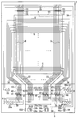
- FIG. 3 is a plan view showing a configuration example of the active matrix substrate.
- FIG. 4 is an enlarged plan view of the mounting area of FIG. 3 and its peripheral part.
- FIG. 5 is an enlarged plan view of the third thin film transistor of FIG. 3 and its peripheral portion.
- FIG. 6 is a diagram illustrating a configuration example of the mounting terminal and its peripheral portion.
- 7 is a cross-sectional view taken along line VII-VII in FIG. 8 is a cross-sectional view taken along line VIII-VIII in FIG.
- FIG. 9 is a cross-sectional view taken along line IX-IX in FIG.
- FIG. 10 is a diagram showing a configuration example of an active matrix substrate according to the second embodiment of the present invention.
- FIG. 11 is an enlarged view of the non-facing region in FIG.
- FIG. 12 is a diagram illustrating a configuration example of the mounting terminal of the gate bus line and its peripheral portion.
- An active matrix substrate includes a plurality of gate bus lines, A plurality of data bus lines provided in different layers through the gate bus line and an insulating film; A first switching element connected to the gate bus line and the data bus line; A mounting terminal for supplying a signal from a driver to the gate bus line or the data bus line; A plurality of lead lines connecting the mounting terminal and the gate bus line or the data bus line; A plurality of second switching elements respectively connected to the plurality of lead lines; A first common wiring connected in common to at least two of the plurality of second switching elements; A plurality of third switching elements connected to an end of the gate bus line or the data bus line to which the mounting terminal is not connected; A second common wiring connected in common to at least two of the plurality of third switching elements.
- the second switching element is connected to a plurality of lead lines connecting the gate bus line or the data bus line and the mounting terminal, and the mounting terminal of the gate bus line or the data bus line is not connected.
- a third switching element is connected to the end.
- the second switching element is connected to the first shared wiring, and the third switching element is connected to the second common wiring.
- the first common wiring may be connected to all of the plurality of second switching elements. Thereby, if there is at least one first common wiring, a signal can be supplied to the second switching element. Therefore, simplification of the wiring configuration on the mounting terminal side becomes easier.
- a plurality of the second common wirings may be provided, and a predetermined number of the third switching elements may be connected to the plurality of second common wirings. Accordingly, it is possible to perform operation processing such as inspection processing and voltage application processing for each predetermined number using the third common wiring, and it is easier to simplify the configuration of the first common wiring on the mounting terminal side. Become.
- the mounting terminal is disposed in a mounting region where the driver is mounted, and the plurality of second switching elements are also disposed in a mounting region where the driver is mounted. It can.
- the second switching elements are compactly integrated in the driver mounting area, and a more efficient arrangement is possible.
- two adjacent lead lines are formed of the same conductive layer as the gate bus line, and the two other lead lines are the data bus. It can be set as the structure formed with the same electroconductive layer as a line. In this case, even if the density of the lead lines increases, it is possible to suppress the occurrence of a short circuit or disconnection of the lead lines.
- the one lead line and the other lead line adjacent to each other are connected to the same conductive layer at the mounting terminal and connected to the first common wiring via the same conductive layer.
- the mounting terminal also serves as a connection changing portion, so that it is not necessary to provide a connection changing portion separately.
- the plurality of lead lines are connected to the common wiring in the same layer, the structure of the common wiring can be simplified.
- the second switching element connected to the data bus line through the lead line and the second switching element connected to the gate bus line through the lead line are in one mounting region or adjacent to each other. It is possible to adopt a configuration that is arranged in a plurality of mounting areas and connected to the same control wiring. This facilitates integration of the second switching elements and simplification of the control wiring.
- an oxide semiconductor is preferably used for each of the first and second switching elements.
- a high-performance and compact switching element can be easily configured, and signal control using the second switching element can be performed with high accuracy.
- a display device is characterized by using any of the active matrix substrates described above.
- the driver mounting area is small, it is possible to maintain the functions of the wiring and elements outside the display area and to efficiently arrange these wirings and elements. Therefore, a high-performance and compact display device can be easily configured.
- FIG. 1 is a diagram for explaining a liquid crystal display device using an active matrix substrate according to the first embodiment of the present invention.
- the liquid crystal display device 1 according to the present embodiment includes a liquid crystal panel 2 in which the upper side of FIG. 1 is installed as a viewing side (display surface side), and a non-display surface side of the liquid crystal panel 2 (lower side of FIG. 1). And a backlight device 3 that generates illumination light for illuminating the liquid crystal panel 2.
- the liquid crystal panel 2 includes a counter substrate 4 constituting the pair of substrates and the active matrix substrate 5 of the present invention, and polarizing plates 6 and 7 provided on the outer surfaces of the counter substrate 4 and the active matrix substrate 5, respectively. Yes. A liquid crystal layer described later is sandwiched between the counter substrate 4 and the active matrix substrate 5.
- the counter substrate 4 and the active matrix substrate 5 are made of a transparent transparent resin such as a flat transparent glass material or an acrylic resin. Resin films such as TAC (triacetyl cellulose) or PVA (polyvinyl alcohol) are used for the polarizing plates 6 and 7 and correspond to cover at least the effective display area of the display surface provided in the liquid crystal panel 2. It is bonded to the counter substrate 4 or the active matrix substrate 5. In some cases, a ⁇ / 4 retardation plate (quarter wavelength plate) is disposed between the polarizing plates 6 and 7 and the liquid crystal layer.
- the active matrix substrate 5 constitutes one of the pair of substrates.
- pixel electrodes and thin film transistors thin film transistors (in accordance with a plurality of pixels included in the display surface of the liquid crystal panel 2) are provided.
- a TFT (Thin Film Transistor) or the like is formed between the liquid crystal layer (details will be described later).
- the counter substrate 4 constitutes the other substrate (counter substrate) of the pair of substrates, and a color filter, a counter electrode, and the like are formed between the liquid crystal layer and the counter substrate 4 ( Not shown).
- the liquid crystal panel 2 is provided with an FPC (Flexible Printed Circuit) 8 connected to a control device (not shown) for controlling the drive of the liquid crystal panel 2 and operates the liquid crystal layer in units of pixels.
- FPC Flexible Printed Circuit
- the display surface is driven in units of pixels and a desired image is displayed on the display surface.
- the liquid crystal mode and pixel structure of the liquid crystal panel 2 are arbitrary. Moreover, the drive mode of the liquid crystal panel 2 is also arbitrary. That is, as the liquid crystal panel 2, any liquid crystal panel that can display information can be used. Therefore, the detailed structure of the liquid crystal panel 2 is not shown in FIG.
- the backlight device 3 includes a light emitting diode 9 as a light source, and a light guide plate 10 disposed to face the light emitting diode 9.
- the light emitting diode 9 and the light guide plate 10 are sandwiched by the bezel 14 having an L-shaped cross section in a state where the liquid crystal panel 2 is installed above the light guide plate 10.
- a case 11 is placed on the counter substrate 4.
- the backlight device 3 is assembled to the liquid crystal panel 2 and is integrated as a transmissive liquid crystal display device 1 in which illumination light from the backlight device 3 is incident on the liquid crystal panel 2.
- the light guide plate 10 for example, a synthetic resin such as a transparent acrylic resin is used, and light from the light emitting diode 9 enters.
- a reflection sheet 12 is installed on the opposite side (opposite surface side) of the light guide plate 10 to the liquid crystal panel 2.
- an optical sheet 13 such as a lens sheet or a diffusion sheet is provided on the liquid crystal panel 2 side (light emitting surface side) of the light guide plate 10, and the inside of the light guide plate 10 has a predetermined light guide direction (left side in FIG. 1). The light from the light emitting diode 9 guided in the direction from the right side to the right side is changed to the planar illumination light having uniform luminance and applied to the liquid crystal panel 2.
- the present embodiment is not limited to this, and a direct type backlight device is used. May be.
- a backlight device having other light sources such as a cold cathode fluorescent tube and a hot cathode fluorescent tube other than the light emitting diode can also be used.
- liquid crystal panel 2 of the present embodiment will be specifically described with reference to FIG.
- FIG. 2 is a diagram for explaining the configuration of the liquid crystal panel shown in FIG.
- the liquid crystal display device 1 includes a panel control unit 15 that performs drive control of the liquid crystal panel 2 (FIG. 1) as the display unit that displays information such as characters and images, and the panel control.
- a data driver (source driver) 16 and a gate driver 17 that operate based on an instruction signal from the unit 15 are provided.
- the panel control unit 15 is provided in the control device, and receives a video signal from the outside of the liquid crystal display device 1. Further, the panel control unit 15 performs predetermined image processing on the input video signal to generate each instruction signal to the data driver 16 and the gate driver 17, and the input video signal. A frame buffer 15b capable of storing display data for one frame included. Then, the panel control unit 15 performs drive control of the data driver 16 and the gate driver 17 according to the input video signal, so that information corresponding to the video signal is displayed on the liquid crystal panel 2.
- the data driver 16 and the gate driver 17 are installed on the active matrix substrate 5. Specifically, the data driver 16 is installed on the surface of the active matrix substrate 5 along the lateral direction of the liquid crystal panel 2 in the outer region of the effective display area A of the liquid crystal panel 2 as a display panel. . Further, the gate driver 17 is installed on the surface of the active matrix substrate 5 so as to be along the vertical direction of the liquid crystal panel 2 in the outer region of the effective display region A. As described in detail later, the gate driver 17 may be divided into two gate drivers provided so as to sandwich the effective display area A, or the gate driver 17 may be the liquid crystal. You may arrange
- the data driver 16 and the gate driver 17 are driving circuits that drive a plurality of pixels P provided on the liquid crystal panel 2 side by pixel, and the data driver 16 and the gate driver 17 include a plurality of data bus lines ( Source wirings) D1 to DM (M is an integer of 2 or more, hereinafter collectively referred to as “D”) and a plurality of gate bus lines (gate wirings) G1 to GN (N is an integer of 2 or more; Are generally connected by "G").
- the data bus lines D and the gate bus lines G are arranged in a matrix so as to intersect each other on a transparent glass material or a transparent synthetic resin substrate described later included in the active matrix substrate 5. Yes.
- the data bus lines D are provided on the substrate so as to be parallel to the matrix column direction (vertical direction of the liquid crystal panel 2), and the gate bus lines G are arranged in the matrix row direction (the liquid crystal panel 2). In the horizontal direction) on the base material.
- a first thin film transistor 18 as a first switching element and a pixel electrode 19 connected to the first thin film transistor 18 are provided.
- the pixel P is provided.
- the counter electrode 20 is configured to face the pixel electrode 19 with the liquid crystal layer provided on the liquid crystal panel 2 interposed therebetween. That is, in the active matrix substrate 5, the first thin film transistor 18 and the pixel electrode 19 are provided for each pixel.
- regions of a plurality of pixels P are formed in regions partitioned by the data bus lines D and the gate bus lines G in a matrix.
- the plurality of pixels P include red (R), green (G), and blue (B) pixels.
- the RGB pixels are sequentially arranged in this order, for example, in parallel with the gate bus lines G1 to GN. Further, these RGB pixels can display corresponding colors by the color filter layer provided on the counter substrate 4 side.
- the gate driver 17 turns on the gate electrode of the corresponding first thin film transistor 18 for the gate bus lines G1 to GN based on the instruction signal from the image processing unit 15a. Scan signals (gate signals) are sequentially output.
- the data driver 16 applies data signals (voltage signals (gradation voltages)) corresponding to the luminance (gradation) of the display image based on the instruction signal from the image processing unit 15a to the corresponding data bus lines D1 to DM. Output to.
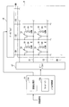
- FIG. 3 is a plan view showing a configuration example of the active matrix substrate.
- the active matrix substrate 5 includes a region covered with the counter substrate 4 (hereinafter referred to as a counter region) and a region not covered with the counter substrate 4 (hereinafter referred to as a non-opposing region).
- an effective display area A is provided in the facing area.
- a plurality of data bus lines D and a plurality of gate bus lines G orthogonal to each other are arranged in a matrix.
- the data bus line D or the gate bus line G refers to a wiring provided in the effective display area A.
- a wiring provided outside the effective display area A and connected to the data bus line D or the gate bus line G is referred to as a lead line or the like.
- the gate drivers 17a and 17b are monolithically formed on the base material of the active matrix substrate 5 at a position sandwiching the effective display area A from the left and right. In all of the plurality of gate bus lines G, the left end is connected to the gate driver 17a, and the right end is connected to the gate driver 17b.
- the gate drivers 17a and 17b are connected to the gate driver driving signal terminal 21b via the gate driver driving signal wiring 21a.
- the gate driver driving signal terminal 21b is connected to the FPC connection terminal of the FPC 8.
- the gate driver 17a, 17b receives an instruction signal from the image processing unit 15a. It is designed to be entered through.
- the configuration of the gate driver is not limited to the above example.
- the plurality of gate bus lines G may be alternately connected to the left and right gate drivers 17a and 17b, or the gate drivers may be provided only on one side with respect to the effective display area A.
- the structure which mounts the gate drivers 17a and 17b which consist of IC chips on the said base material may be sufficient.
- an auxiliary capacitance electrode CS for generating a predetermined auxiliary capacitance for each pixel P is provided.
- the auxiliary capacitance electrode CS is connected to the auxiliary capacitance electrode driving signal terminal CS2 via the auxiliary capacitance electrode driving signal wiring CS1.
- the auxiliary capacitor electrode drive signal terminal CS2 is connected to the FPC connection terminal of the FPC 8. A voltage is supplied from the FPC 8 to the auxiliary capacitance electrode CS.
- the auxiliary capacitance electrode CS constitutes a common electrode, is formed of a transparent electrode material, and is provided below the pixel electrode 19.
- the data driver 16 can be constituted by, for example, an IC chip (driver chip). Outside the effective display area A, the active matrix substrate 5 is mounted on the base material 5a. A rectangular area indicated by a broken line DA in FIG. 3 is a data driver mounting area. In this example, the mounting area is arranged in the non-facing area. When the data driver is mounted, the mounting area is covered with the data driver.
- bumps (electrodes) of the data driver 16 are connected to mounting terminals DT3 and DT4 connected to the data bus line D of the active matrix substrate 5 and mounting terminals 28a for connecting to the FPC 8. ing.
- a lead wire 22 is connected to each data bus line D, and each lead wire 22 is connected to a mounting terminal DT3 or DT4.
- the lead line 22 is wired in an oblique direction with respect to the data bus line D. That is, the lead-out lines are aggregated from the data bus line D to the mounting terminals DT3 and DT4 that are arranged at a narrower interval than the interval of the data bus line D. Thereby, the mounting area
- positioned can be made small.
- a portion where the lead wire 22 wired in an oblique direction with respect to the data bus line D is arranged is called a fan-out portion (an oblique portion).
- the input mounting terminal 28a on the FPC side is connected to the data driver driving signal terminal 28c through the data driver driving signal wiring 28b.
- the data driver drive signal terminal 28c is connected to the FPC connection terminal of the FPC 8. Thereby, an instruction signal from the image processing unit 15a is input to the data driver 16 via the FPC 8.
- a second thin film transistor 45 which is an example of a second switching element, is connected to each of the mounting terminals DT3 and DT4 connected to the data bus line D via the lead line 22.
- a control line 46 for transmitting a control signal for controlling ON / OFF of the second thin film transistor 45 is connected to the plurality of second thin film transistors 45.
- the control line 46 is connected to the terminal 46a, and the terminal 46a is further connected to the input terminal 46c via the wiring 46b.
- the plurality of second thin film transistors 45 are connected to a first common wiring 47 for transmitting a signal input to the data bus line D via the second thin film transistors 45.
- one first common wiring 47 is connected to all the plurality of second thin film transistors 45 connected to the data bus line D.
- a terminal 47 a is connected to the first common wiring 47.
- the terminal 47a is connected to the input terminal 47c through the wiring 47b.
- the FPC connection terminals of the FPC 8 are connected to the input terminals 47c and 46c.
- the second thin film transistor 45 As described above, in the example illustrated in FIG. 3, with respect to the data bus line D, on the data driver 16 (driver chip) side, the lead line 22, the mounting terminals DT ⁇ b> 3 and DT ⁇ b> 4, the second thin film transistor 45, Common wiring 47, terminal 47a, wiring 47b, and input terminal 47c are sequentially connected. With this configuration, it is possible to input a signal to the data bus line D via the second thin film transistor 45 independently of the drive signal input from the driver via the mounting terminals DT3 and DT4. That is, a signal system different from the signal input system from the driver can be separately provided for the data bus line D.
- a voltage for an inspection signal for the data bus line D or a voltage application process for orientation control can be input from the terminal 47a or the input terminal 47c.
- the input terminal 47c is connected to the ground via the FPC 8, and a signal for turning off each second thin film transistor 45 is supplied to the input terminal 46c. Can be entered.
- a third thin film transistor 52 which is an example of a third switching element, is connected to the end of the data bus line D on the side where the mounting terminals DT3 and DT4 are not connected.
- the third thin film transistors 52 are connected to the plurality of data bus lines D, respectively.
- Each of the plurality of third thin film transistors 52 is connected to one of the three second common wirings 54.
- the second common wiring 54 is connected to the terminal 55.
- the end of the data bus line D on the side where the mounting terminal DT3 or DT4 is not connected is drawn out of the effective display area A by a plurality of lead lines 51.
- the third thin film transistor 52 connected to each of the plurality of lead lines 51 is connected to the second common wiring 54 via the connection wiring 53.
- the lead line 51, the third thin film transistor 52, the connection wiring 53, the three second common wirings 54, and the terminal 55. are connected sequentially.
- input / output of signals to and from the data bus line D can be performed in three systems under the control of the third thin film transistor 52 independently of the driver drive signal.
- the connection configuration of the third thin film transistor 52 is not limited to the example illustrated in FIG. 3.
- the third thin film transistor 52 may be connected to the data bus line D at the boundary of the effective display area A.
- the third thin film transistor 52 is connected to a control line 56 for transmitting a control signal for controlling ON / OFF.
- the gate electrode (not shown) is configured integrally with the control line 56.
- a terminal 57 is connected to the control line 56, and this terminal 57 is connected to an input terminal 58 through a wiring.
- the input terminal 58 is connected to the FPC connection terminal of the FPC 8.
- a control signal for performing ON / OFF operation of the third thin film transistor 52 is input from the terminal 57 or the input terminal 58 and input to the data bus line D.
- the signal is input from the terminal 55.
- a signal for turning off each third thin film transistor 52 is input to the input terminal 58 via the FPC 8.
- the first common wiring 47 is connected to the mounting terminals DT3 and DT4 connected to the data bus line D via the second thin film transistor 45, and the mounting terminal of the data bus line D is connected.
- the side where no is provided is connected to the second common wiring 54 through the third thin film transistor 52.
- all the second thin film transistors 45 connected to the mounting terminals DT3 and DT4 are all connected to one common wiring 47, and the third thin film transistors 52 on the side where no mounting terminal is provided. Is connected to one of the plurality of second common wires. That is, a predetermined number of third thin film transistors 52 are connected to each of the plurality of second common wires.
- the second common wiring 54 can be provided for each RGB color. These second common wirings 54 can be connected to the data bus lines D corresponding to the respective RGB colors via the third thin film transistors 52 for each of the RGB colors. That is, the data bus lines corresponding to RGB colors are connected to different second common lines 54. Thereby, for example, the inspection operation of the data bus line D can be performed for each color of RGB.
- one first common wiring 47 is provided on the input side of the data bus line D (that is, the driver chip mounting region side). In the inspection operation using the first common wiring 47, it is possible to detect the disconnection of each of the data bus line D and the lead line 22, the defect of the first thin film transistor 18, and the like. However, with only this one system, it is not possible to perform monochrome display for each of RGB, and it is also impossible to detect a short circuit between adjacent data bus lines D or between adjacent lead lines 22.
- the active matrix substrate 5 of the present embodiment for example, it is possible to apply a voltage from the second common wiring 54 during the alignment process of the liquid crystal layer (voltage application process for implementing the PSA technique). is there. In that case, the time required for the alignment treatment can be shortened by simultaneously applying a voltage from the first common wiring 47.
- the PSA technique is a technique for forming an alignment maintaining layer (Alignment Sustaining Layer) that gives a pretilt to the liquid crystal when no voltage is applied in order to regulate the alignment direction of the liquid crystal molecules when no voltage is applied.
- This alignment maintaining layer is formed by forming a liquid crystal cell and then photopolymerizing a photopolymerizable monomer (or oligomer) premixed in a liquid crystal material, typically with a voltage applied to the liquid crystal layer. Formed as a layer.
- FIG. 4 is an enlarged plan view of a mounting area of the data driver shown in FIG. 3 and its peripheral portion.
- FIG. 5 is an enlarged plan view of the third thin film transistor 52 shown in FIG. 3 and its peripheral portion.
- a gate layer wirings and terminals formed in the same layer (hereinafter referred to as a gate layer) where the gate bus line G is formed are indicated by dotted lines.
- Wirings and terminals formed on a layer different from the layer of the gate bus line G with an insulating film for example, the same layer as the data bus line D (hereinafter referred to as a source layer)
- a point where the wiring formed in the source layer and the wiring formed in the gate layer are connected is represented by a black circle.
- the lead lines 22 drawn from the data bus line D two adjacent lead lines 22 are formed in different layers. Thereby, in the fan-out part FA, even when the interval between the lead lines 22 is narrowed, the lead lines are not easily short-circuited or disconnected. In particular, since the lead lines 22 are collected in the mounting area, the distance between the lead lines 22 becomes narrower as the mounting area is approached. By arranging the lead lines 22 in different layers alternately, it is possible to suppress the occurrence of a short circuit or disconnection between adjacent lead lines.
- the lead lines 22 formed in different layers adjacent to each other are connected to the second thin film transistor 45 by being connected to the same conductive layer (here, the source layer) at the mounting terminal DT3 or DT4.
- the mounting terminal DT3 or DT4 and the second thin film transistor 45 are connected by the wiring connected to the source layer by the mounting terminals DT3 and DT4.
- the first common wiring 47 is formed in the gate layer. Therefore, the second thin film transistor 45 and the first common wiring 47 are connected via the source layer wiring and the contact hole connecting the source layer and the gate layer.
- the mounting terminals DT3 and DT4 also serve as a connection changing function, it is not necessary to provide a connection changing part separately. Further, in the mounting terminals DT3 and DT4, the lead line 22 formed in the gate layer is switched from the gate layer to the source layer, so that the lead line 22 in a state separated into the gate layer and the source layer in the fan-out portion FA is lengthened. Can be secured. For this reason, it is possible to reduce the probability that adjacent lead wires 22 are short-circuited. Further, by connecting the plurality of mounting terminals DT3, DT4 to the first common wiring 47 via the same layer wiring, the configuration of the plurality of second thin film transistors 45 and the first common wiring 47 is simplified. can do. For example, in the example shown in FIG.
- a plurality of layers in the source layer are compared with the first common wiring 47 having a simple configuration linearly formed by one line in one layer (a gate layer in this example).
- the second thin film transistors 45 are connected to each other through contact holes. Further, the structure of the control line 46 of the second thin film transistor 45 can be simplified by being formed integrally with the gate electrodes of the plurality of thin film transistors 45 formed in the gate layer.
- the mounting terminals DT3 and DT4 are provided in the mounting area of the data driver 16 indicated by DA. It can arrange efficiently.
- lead lines 51r, 51g, and 51b are provided for each RGB color.
- the lead lines 51r, 51g, and 51b are respectively connected to the end portions of the RGB data bus line D on the non-input side (the side where no mounting terminal is provided).
- a drain electrode (not shown) of the third thin film transistor 52 is connected to each of the lead lines 51r, 51g, and 51b.
- the source electrode (not shown) of the third thin film transistor 52 is connected to the second common wirings 54r, 54g, and 54b provided for each of the RGB colors via the connection wirings 53r, 53g, and 53b.
- the lead lines 51r, 51g, 51b and the connection lines 53r, 53g, 53g are all formed so as to extend in the same direction as the data bus line D.
- All the gate electrodes of the third thin film transistors 52 are connected to one control line 56. Specifically, the gate electrodes and the control lines 56 of all the third thin film transistors 52 are integrally formed in the gate layer.
- corresponding lead lines 51r, 51g, and 51b are connected via the third thin film transistor 52 for each of RGB colors. That is, a predetermined number of third thin film transistors 52 are connected for each RGB, and a predetermined number of RGB data bus lines D are connected.
- the RGB data bus line D is connected to the second common wirings 54r, 54g, and 54b for each of the RGB colors. For this reason, different signals can be input for each of the RGB data bus lines D, and operations can be performed independently of each other.
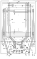
- FIG. 6 is a diagram illustrating a configuration example of the mounting terminal and its peripheral portion.
- 7 is a cross-sectional view taken along line VII-VII in FIG. 8 is a cross-sectional view taken along line VIII-VIII in FIG. 9 is a cross-sectional view taken along line IX-IX in FIG.
- the portions where wirings are provided in the gate layer are indicated by dots.
- lead lines 22r, 22g, and 22b respectively corresponding to, for example, RGB colors are sequentially arranged along the horizontal direction of the figure.
- Each lead line 22r, 22g, and 22b is connected to the mounting terminal DT3 or DT4.
- Bumps (electrodes) of the data driver 16 are connected to the mounting terminals DT3 and DT4.
- the mounting terminals DT3 and DT4 are provided in a two-stage staggered arrangement. That is, the mounting terminals DT3 and DT4 connected to the two adjacent lead lines are arranged so as to be shifted from each other in the direction of the lead line, and the two lead lines arranged on both sides of the one lead line are arranged.
- the mounting terminals to be connected are arranged at adjacent positions without being displaced in the lead line direction. Thereby, the plurality of mounting terminals DT3 and DT4 can be efficiently arranged, and the probability of occurrence of a short circuit in the vicinity of the two adjacent mounting terminals DT3 and DT4 can be reduced.
- two adjacent one lead lines 22 are formed of the same conductive layer as the gate bus line G, and the other two adjacent data bus line lead lines 22 is formed of the same conductive layer as the data bus line D.
- two adjacent lead lines 22 are formed in the gate layer on the active matrix substrate 5, and the other two adjacent lead lines 22 are gate insulating films 29 covering the gate layer. Is formed in the source layer above.
- the lead line 22 formed of the same conductive layer as the gate bus line G is connected to the second terminal lower layer electrode formed of the same conductive layer as the data bus line D, so that the second thin film transistor It is connected to the drain electrode. That is, the mounting terminal DT3 has a function of connecting the lead wire 22 to a different layer. This specific configuration will be described later with reference to FIG.
- the second thin film transistor 45 includes a drain electrode 45d connected to the lead line 22 and a source electrode 45s provided at a position facing the drain electrode 45d in the same layer as the drain electrode 45d. Under the drain electrode 45d and the source electrode 45s, a semiconductor layer 45h is provided at a position overlapping with these. In the lower layer of the semiconductor layer 45h, a gate electrode 45g is provided at a position overlapping the semiconductor layer 45h. The gate electrode 45g is formed integrally with the control line 46 in the gate layer. The plurality of second thin film transistors 45 share a gate electrode formed continuously with the control line 46.
- width details 22a each having a narrow width dimension are provided at portions overlapping the gate electrode formed integrally with the control line 46, respectively.
- width details 50a each having a narrow width dimension are provided at portions overlapping the gate electrode formed integrally with the control line 46, respectively.
- the width details 22a and 50a By providing the width details 22a and 50a, the area where the control line 46 and the lead lines 22r, 22g and 22b overlap and the area where the control line 46 and the connection lines 50r, 50g and 50b overlap are suppressed. Can do.
- signal delay in the data bus line D can be suppressed, and deterioration of display quality after the data driver 16 is mounted on the chip (that is, the final product of the liquid crystal display device 1) can be prevented.
- the delay of the inspection control signal with respect to the control line 26 can be suppressed at the time of inspection, display unevenness can be easily reduced when inspection display is performed, and erroneous detection of defects can be suppressed. Can do.
- a control line 46 (gate electrode) is formed in a region sandwiched between two second thin film transistors 45 arranged on both sides of one lead line 22 or connection wiring 50. There is a portion 46d that is not. That is, a gate electrode is provided in a part of a region sandwiched between two thin film transistors arranged with the lead line 22 or the connection wiring 50 interposed therebetween so that a control signal can be easily transmitted between the two thin film transistors. By removing the gate electrode, the area where the lead line 22 or the connection wiring 50 and the gate electrode overlap can be reduced.
- the second thin film transistor 45 has a two-stage staggered arrangement so as to match the mounting terminals DT3 and DT4. That is, two thin film transistors connected to two adjacent lead lines are arranged so as to be shifted from each other in the direction of the lead line, and are connected to two lead lines arranged on both sides of one lead line. The thin film transistors are arranged in adjacent positions without being displaced in the lead line direction. Further, the second thin film transistor 45 is arranged so as to shift in accordance with the shift of the mounting terminals DT3 and DT4. Thereby, the plurality of mounting terminals DT3 and DT4 and the second thin film transistor 45 can be efficiently arranged, and the probability that a short circuit occurs in the vicinity of the two adjacent second thin film transistors 45 can be reduced.
- connection wirings 50r, 50g, or 50b provided for each of RGB is connected to the source electrode 45s of the second thin film transistor 45.
- the connection wirings 50r, 50g, and 50b are formed in the source layer, and the first common wiring 47 is formed in the gate layer. Therefore, the first common wiring 47 is connected to the connection wirings 50r, 50g, and 50b via the terminal contact hole H3.
- the first common wiring 47 is formed by a single line extending linearly in a direction perpendicular to the lead line 22 and the connection wiring 50. Further, in the portion where the connection wirings 50r, 50g, 50b overlap with the first common wiring 47, each connection wiring 50r, 50g, 50b is connected to the adjacent connection wiring. As a result, the connection wiring 50 is integrally formed along the first common electrode 47. A terminal contact hole H3 is provided in the integrally formed portion.
- the first common wiring 47 when adjacent connection wirings are interconnected on the first common wiring 47, the first common wiring can be reduced in resistance, so that the outer shape of the display device (for example, the driver mounting region) is further increased. Even small cases can be accommodated. Further, when the first common wiring 47 is disconnected, the interconnecting portion of the connection wiring functions as a redundant wiring, so that defective products at the time of manufacturing can be reduced.
- FIG. 7 shows an example of a configuration in which the lead line 22g drawn from the data bus line D through the gate layer is connected to the source layer at the mounting terminal DT3.
- the lead line 22g is formed of the same conductive layer as the gate bus line G on the base material 5a of the active matrix substrate 5 between the data bus line D and the mounting terminal DT3 (FIG. 7). Right end side).
- the end of the lead wire 22g is used as the first terminal lower layer electrode 36a in the mounting terminal DT3.
- the second terminal lower layer electrode 36b formed of the same conductive layer as the data bus line D and the terminal upper layer electrode 34 are provided on the first terminal lower layer electrode 36a.
- the second terminal lower layer electrode 36b is connected to the drain electrode 45d (see FIG. 9) of the second thin film transistor 45 as the lead line 22g.
- the terminal upper layer electrode 34 can be formed of, for example, the same conductive layer as the pixel electrode 19.
- the lead line 22 formed of the same conductive layer as the gate bus line G is connected to the lead line 22 of the same conductive layer as the data bus line D and is connected to the second thin film transistor 45.
- a gate insulating film 29, a channel protective layer 30, and interlayer insulating films 31 and 33 are provided on a lead line 22g formed of the same conductive layer as the gate bus line G.
- the first terminal lower layer electrode 36a and the first terminal electrode Ha are formed through the terminal contact hole H2a formed by hollowing out the gate insulating film 29, the channel protective layer 30, and the interlayer insulating films 31 and 33.
- the second terminal lower layer electrode 36b is connected to each other, and the second terminal lower layer electrode 36b and the terminal upper layer electrode 34 are connected to each other.
- connection from the lead line 22 formed of the same conductive layer as the gate bus line G to the same conductive layer as the data bus line D can be performed in the terminal contact hole H2a. For this reason, it is possible to omit the installation of the area for reconnection, and the external dimensions of the active matrix substrate 5 can be easily reduced.
- FIG. 8 shows a configuration example when the lead-out line 22g is formed of the same conductive layer as the data bus line D between the data bus line D and the mounting terminal DT4.
- the lead line 22 is provided on the gate insulating film 29 and the channel protective layer 30 provided on the substrate 5a.
- the first terminal lower layer electrode 37a is formed of the same conductive layer as the gate bus line G on the base material 5a.
- the lead wire 22g is used as the second terminal lower layer electrode 37b in the mounting terminal DT3.
- the second terminal lower layer electrode 37b is connected to the drain electrode 45d (see FIG. 9) of the second thin film transistor 45.
- H2b, the first terminal lower layer electrodes 36a, 37a and the second terminal lower layer electrodes 36b, 37b are connected to each other, and the second terminal lower layer electrodes 36b, 37b and the terminal upper layer electrode 34 are connected to each other.
- the mounting terminals DT3 and DT4 have the same configuration regardless of the configuration of the lead wires 22, thereby facilitating the inspection of the mounting state of the data driver (driver) 16 on the mounting terminals DT3 and DT4. be able to.
- the connection between the driver chip of the data driver 16 and the mounting terminal DT3 or DT4 is made through an anisotropic conductive film (ACF).
- ACF anisotropic conductive film
- an indentation inspection of conductive particles contained in the layer is performed. This indentation inspection is performed by observing the uneven shape formed on the mounting terminal DT3 or DT4 by the conductive particles from the back surface of the active matrix substrate 5, and conducting particles between the driver chip (bumps thereof) and the mounting terminals DT3 or DT4. This is a test to measure the number of If the film configurations of the mounting terminals DT3 and DT4 are different, the determination becomes complicated, but the determination is simplified by making the film configurations of the mounting terminals DT3 and DT4 the same as in the above configuration. be able to.
- FIG. 9 is a diagram showing a cross-sectional configuration example of the second thin film transistor 45 portion.
- the gate electrode 45g formed integrally with the control line 46 is formed on the gate layer on the substrate 5a.
- An insulating film 29 is formed so as to cover the gate electrode 45g, and a semiconductor layer 45h is provided above the gate electrode 45g with the insulating film 29 interposed therebetween.
- a channel protective layer 30 is provided so as to cover the semiconductor layer 45h. In the portion where the semiconductor layer 45h and the drain electrode 45d provided thereon overlap, the channel protection layer 30 is partially removed, and the semiconductor layer 45h and the drain electrode 45d are connected in that portion.
- the channel protection layer 30 is partially removed, and the semiconductor layer 45h and the source electrode 45s are connected in that portion.
- Interlayer insulating films 31 and 33 are provided so as to cover the drain electrode 45d and the source electrode 45s.
- the source electrode 45s is formed in the source layer in the same manner as the drain electrode 45d.
- the source electrode 45s constitutes an end portion of the connection wiring 50g.
- the semiconductor layer 45h can be formed of, for example, an oxide semiconductor.
- the semiconductor layer of the first thin film transistor 18 can also be formed using an oxide semiconductor.
- the gate electrode 45g of the second thin film transistor 45 in the gate layer is, for example, the same metal material as the gate electrode of the first thin film transistor 18 provided in the effective display region (a single layer or a plurality of kinds of stacked metal materials). And it can form on the base material 5a by the same manufacturing process.
- at least one of the lead line 22 of the gate layer, the control line 46, the first terminal lower layer electrodes 36a and 37a, and the first common wiring 47 is also the same metal material as the gate electrode of the first thin film transistor 18. And can be formed in the same manufacturing process.
- At least one of the lead line 22, the second terminal lower electrodes 36b and 37b, the source electrode 45s, the drain electrode 45d, and the connection wiring 50 in the source layer is, for example, the source electrode of the first thin film transistor 18 and It can be formed by the same metal material as the drain electrode (single layer or plural kinds of stacked metal materials) and the same manufacturing process.
- the present invention is not limited to the above embodiments.
- the second and third thin film transistors 45 and 52 and the first and second common wirings 47 and 54 are connected to the data bus line D, but the gates are used instead of the data bus lines.
- a configuration in which these are connected to the bus line is also possible.
- FIG. 10 is a diagram showing a configuration example of an active matrix substrate according to the second embodiment of the present invention.
- the first embodiment is an example of a configuration in which the gate driver is formed monolithically on the active matrix substrate 5.
- the present embodiment is an example of a configuration in which both a gate driver and a data driver are provided in one driver chip. Therefore, in the configuration example shown in FIG. 10, the mounting terminals connected to the data bus line D and the mounting terminals connected to the gate bus line G are arranged side by side in the non-facing region.
- the mounting terminal connected to the data bus line D and the mounting terminal connected to the gate bus line G are arranged in one driver mounting area.
- a driver mounting area is a driver mounting area.
- a driver chip (not shown) in which a gate driver and a data driver are integrally formed is mounted in this mounting area.
- the gate driver and the data driver can also be configured by independent driver chips.
- the gate driver mounting area and the data driver mounting area are arranged side by side.
- each of the plurality of data bus lines D is connected to a lead line 22, and the lead line 22 is connected to the mounting terminal DT3 or DT4, respectively.
- a second thin film transistor 45 is connected to the mounting terminal DT3 or DT4.
- the plurality of second thin film transistors 45 are all connected to one common wiring.
- a control line 46 for sending a control signal to the second thin film transistor 45 is also connected to the gate electrodes of the plurality of second thin film transistors 45.
- the first common wiring 47 may be connected to a terminal 47a, and the terminal 47a may be further connected to an input terminal (not shown) via a wiring (not shown).
- the control line 46 is connected to the terminal 46a, and the terminal 46a is further connected to the input terminal 46c via the wiring 46b.
- the control line 46 is also connected to the gate electrode of the second thin film transistor 41 connected to the gate bus line G.
- a plurality of second common wirings are respectively connected via the third thin film transistors 52, as in the first embodiment. 54 is connected.
- a control line 56 is connected to the gate electrode of the third thin film transistor 52.
- a lead line 38 is connected to the plurality of gate bus lines G.
- the gate bus lines G are alternately arranged such that the lead line 38 is connected to one end side (left side of the effective display area A) and the lead line 38 is connected to the other end side (right side).
- the lead line 38 passes through the left and right areas of the effective display area A and is connected to the mounting terminal 43 in the non-facing area.
- the mounting terminals 43 connected to the gate bus line G are arranged on both sides of the mounting terminals DT3 and DT4 connected to the data bus line D. In other words, the mounting terminals DT3 and DT4 are arranged in the central portion on the effective display area side in the non-facing area, and the mounting terminals 43 are arranged side by side on the left and right sides thereof.
- the lead line 38 connected from the left side of the gate bus line is connected to the mounting terminal 43 arranged on the left side of the mounting terminals DT3 and DT4 of the data bus line, and the leading line 38 connected from the right side is connected to the mounting terminal 43. It is connected to a mounting terminal 43 arranged on the right side of DT3 and DT4.
- the second thin film transistor 41 for the gate bus line is connected to the mounting terminal 43.
- Each second thin film transistor 41 is connected to one of a plurality (four in this example) of first common wirings 39.
- the first common wiring 39 is connected to the terminal 39e.
- a control line 46 is connected to the plurality of second thin film transistors 41.
- the control line 46 is also connected to the second thin film transistor 45 for the data bus line.
- the data bus line D has a configuration in which a plurality of signal paths are added to the side where the mounting terminal is not provided and one signal path is provided on the mounting terminal side.
- a plurality of signal paths are added to the left and right sides of the gate bus line G. Also with this configuration, it is possible to realize highly accurate and diverse signal control in the signal system while efficiently arranging wiring and elements for the signal system independent of the signal system from the driver.
- the storage capacitor electrode drive signal terminal CS2 is close to the mounting terminal of the data bus line D so that the resistance of the storage capacitor electrode drive signal line CS1 does not increase (that is, the wiring length does not increase).
- the common electrode signal line is often not arranged near the mounting terminal of the gate bus line G. Therefore, as shown in FIG. 10, a plurality of signal paths are added in the vicinity of the mounting terminal of the gate bus line G to enable more precise and diverse signal control and the mounting terminal of the data bus line D.
- the DT3 and DT4 side can be simplified by using one system.
- the additional form of the signal system is not limited to the example shown in FIG.
- the form of an additional signal system for the data bus line or the gate bus line can be modified.
- the gate bus line G one system can be added on the side of one mounting terminal 43 of the left and right, and a plurality of systems can be added on the side of the other mounting terminal 43.
- both the gate bus line G and the data bus line D one system can be added on one side and a plurality of systems can be added on the other side.
- FIG. 11 is an enlarged view of a non-facing region of the active matrix substrate 5 shown in FIG.
- the lead line 22, the mounting terminals DT3 and DT4, the second thin film transistor 45, and the first common wiring 47 connected to the data bus line D are the same as the example shown in FIG. 3 in the first embodiment. It can be constituted as follows.
- wirings and terminals formed in the gate layer are indicated by dotted lines, and wirings and terminals formed in the source layer are indicated by solid lines.
- a point where the wiring formed in the source layer and the wiring formed in the gate layer are connected is represented by a black circle.
- the lead line 38 between the gate bus line G and the mounting terminal 43 includes a lead line formed of the same conductive layer as the gate bus line G and a conductive layer same as the data bus line D. And a formed lead line. That is, in the lead line 38, two adjacent lead lines (38b) (for example, 38a and 38b) are formed in the gate layer, and the other two lead lines (38a) are formed in the source layer. Is done.
- the lead lines 38 b and 38 d formed in the gate layer are connected to the source layer by the mounting terminal 43.
- the mounting terminal 43 and each second thin film transistor 41 are connected by a wiring formed in the source layer.
- the gate electrode of the second thin film transistor 41 is connected to a control line 46 formed in the gate layer.
- the gate electrodes of all the second thin film transistors 41 connected to the gate bus line G are connected to one control line 46.
- the control line 46 is formed to extend linearly in the direction in which the mounting terminals 43 of the gate bus lines and the mounting terminals DT3 and DT4 of the data bus lines are arranged.
- the control line 46 is also connected to the gate electrodes of all the second thin film transistors 45 connected to the data bus line D. In this way, by providing the control line 46 so as to cross the mounting area and arranging the second thin film transistors 41 and 45 along the control line 46, an efficient arrangement can be realized.
- Each second thin film transistor 41 is connected to any one of a plurality (four in this example) of first common wires 38a, 38b, 38c, and 38d. That is, a plurality of first common wires are provided, and each first common wire is connected to a predetermined number of second thin film transistors 41. Thereby, a different signal can be input for each of the predetermined number of second thin film transistors 41.
- first common wirings 39 are connected to different first common wirings 39, respectively.
- the lead lines 38b and 38d are both formed of the same conductive layer as the gate bus line G, but these lead lines 38b and 38d are connected to different first common lines 39b and 39d.
- the lead lines 38a and 38c are both formed of the same conductive layer as the data bus line D. However, the lead lines 38a and 38c are connected to different first common lines 39a and 39c.
- the first common wiring 39 is used in each of the lead line 38 formed of the same conductive layer as the gate bus line G and the lead line 38 formed of the same conductive layer as the data bus line D.
- the mounting terminals of the gate bus line G are provided in the driver mounting area. 43, the second thin film transistor 41, and the first common wiring 39 can be arranged efficiently.
- FIG. 12 is a diagram illustrating a configuration example of the mounting terminal 43 of the gate bus line and its peripheral portion.
- the mounting terminal 43a can be the same as the configuration shown in FIGS. 6 and 7, and the mounting terminal 43b can be the same as the configuration shown in FIGS.
- the drain electrode 41d, the source electrode 41s, the semiconductor layer 41h, and the gate electrode 41g of the second thin film transistor 41 in FIG. 12 can have the same structure as that shown in FIGS.
- Connection wires 42a, 42b, 42c, and 42d are connected to the source electrode 41s of the second thin film transistor 41.
- the connection wirings 42a, 42b, 42c, and 42d formed in the source layer are connected to the first common wirings 39a, 39b, 39c, and 39d formed in the gate layer through the terminal contact holes H5a, H5b, H5c, and H5d. Connected.
- first common wirings 39a, 39b, 39c, and 39d extending in a direction perpendicular to the lead line 38 or the connection wiring 42 are arranged in order.
- the first common wiring 39a and the first common wiring 39c adjacent to the first common wiring 39a are connected to a predetermined number of second thin film transistors 41 via a predetermined number of terminal contact holes H5a and H5c and source layer connection wirings 42a and 42c. Connected to.
- the predetermined number of second thin film transistors 41 are connected to the predetermined number of gate bus lines G through the mounting terminals 43b and the source layer lead lines 38a and 38c.
- the common wirings 39b and 39d adjacent to the first common wirings 39a and 39c are connected to the mounting terminals 43a through a predetermined number of terminal contact holes H5b and H5d, source layer connection wirings 42b and 42d, and a predetermined number of second thin film transistors 41.
- a predetermined number of terminal contact holes H5b and H5d Source layer connection wirings 42b and 42d
- a predetermined number of second thin film transistors 41 are connected to the lead lines 38b and 38d of the gate layer at the mounting terminal 43a and connected to a predetermined number of gate bus lines G.
- two adjacent lead lines ie, 38a and 38b, 38b and 38c, 38c and 38d, 38d and 38a
- two adjacent first common wires 39a and 39b, 39b and 39c, 39c.
- 39d and 39d and 39a respectively.
- two adjacent lead lines (38a and 38c, 38b and 38d) in the same layer are connected to two different first common lines (39a and 39c, 39b and 39d).
- the third thin film transistor (third switching element) 52 connected to the end of the data bus line D on the side where the mounting terminal DT3 or DT4 is not connected, A second common wiring 54 connected in common to the plurality of third thin film transistors 52 is provided.
- the configuration on the mounting terminal DT3 or DT4 side such as the configuration of the first common wiring 47, can be simplified.
- the second thin film transistor (second switching element) 45 can be arranged more easily. Furthermore, according to the above-described embodiment, it is possible to reduce the mounting area of the driver.
- the auxiliary capacitance electrode driving signal wiring CS1 of the auxiliary capacitance electrode (common electrode) CS is enlarged, that is, the auxiliary capacitance electrode driving signal wiring CS1 is made thicker, and the auxiliary capacitance electrode driving signal wiring is increased.
- the resistance of CS1 can be reduced. As a result, it is possible to suppress the occurrence of display defects such as flicker and shadowing due to the delay of the signal (voltage signal) to the auxiliary capacitance electrode CS.
- two or more data bus lines or gate bus lines via the third thin film transistor 52 are provided on the non-input side (the side where no mounting terminal is provided).
- the outer shape of the display device for example, the driver mounting area
- the thin film transistor 45 is small by disposing a single signal path through the thin film transistor 45 on the mounting terminal side with respect to the active matrix substrate 5 on which the signal path is formed. Even in this case, it is possible to control the input / output of signals for a range that covers not only the data bus line or gate bus line but also the lead line.
- the effect of performing an inspection using the added system will be described.
- the data bus line or the gate bus line is mounted.
- the disconnection of the lead wire between terminals cannot be inspected.
- it is possible to detect disconnection of the leader line by adding one or more signal paths on the mounting terminal side and two or more signal paths on the side where the mounting terminal is not provided. .
- the arrangement region of the second thin film transistor 45 may be narrower than the region necessary for laser cutting.
- the width necessary for laser cutting is about 200 ⁇ m, whereas in the example shown in FIG. 6, for example, the arrangement region of the second thin film transistor 45 may be about 78 ⁇ m.
- first common wires 47 may be provided. That is, the first common wiring may be connected to at least two of the plurality of second thin film transistors 45. Further, the number of second common wires 54 is not limited to three, and the number of first common wires 39 is not limited to four.
- the second thin film transistor and the first common wiring may be provided between the fan-out portion or the mounting terminal and the fan-out portion.
- the configuration of the mounting terminals is not limited to the above example. Instead of reconnecting with the mounting terminals, a reconnecting part can be provided separately.
- the structure which covers a part of 2nd thin-film transistor connected to a mounting terminal may be sufficient as the terminal upper electrode of a mounting terminal.
- the data bus line D is provided on the gate bus line G via the gate insulating film 29.
- the gate bus line G may be provided on the data bus line D via the insulating film.
- the bus line G in the horizontal direction on the paper is the gate bus line and the bus line D in the vertical direction on the paper is the data bus line.
- the bus lines G may be switched.
- the bus line indicated by G in FIG. 10 (the bus line in the horizontal direction on the paper) may be a data bus line
- the bus line indicated by D (the bus line in the vertical direction on the paper) may be a gate bus line.
- the mounting terminal of the data bus line is provided below the effective display area, but the position of the mounting terminal is not limited to this.
- the mounting terminal may be provided on at least one side of the effective display area on the left or right.
- the active matrix substrate of the present invention is not limited to this, and an effective display area having a plurality of pixels and pixels
- the active matrix substrate of the present invention can be applied to any display device having a wiring for transmitting a signal for driving the signal.
- the present invention can be applied to an organic EL display, a microcapsule-type electrophoresis display device, and other display devices.
- a microcapsule-type electrophoresis display device can be configured to display an image, for example, by applying a voltage to each microcapsule layer formed in an effective display region for each pixel.
- the display device includes, for example, a substrate including a wiring of an effective display region connected to a pixel electrode provided for each pixel via a switching element, and a lead line connected to the wiring of the effective display region.
- this substrate can be configured like the active matrix substrate in the above embodiment.
- the active matrix substrate of the present invention can be applied to various sensor substrates such as a sensor substrate for an X-ray detection device.
- the configuration in which the mounting terminals DT are arranged in a two-stage staggered arrangement has been described.
- the active matrix substrate of the present invention is not limited to this.
- the mounting terminals DT are arranged in a three-stage staggered arrangement. (In other words, three adjacent mounting terminals DT may be sequentially shifted so as to be arranged at different positions in the linear direction.)
- This embodiment can be applied to, for example, a CPA mode liquid crystal panel (a so-called vertical electric field liquid crystal panel) which is a kind of vertical alignment mode, but is not limited thereto.
- a CPA mode liquid crystal panel a so-called vertical electric field liquid crystal panel
- the present invention can also be applied to other vertical alignment mode liquid crystal panels using fishbone pixel electrodes and horizontal alignment mode liquid crystal panels (so-called lateral electric field liquid crystal panels).
- the fishbone type pixel electrode can be represented by an azimuth angle that takes a positive angle counterclockwise with the right direction in the horizontal direction (direction in which the gate bus line extends) being 0 °, for example, 45 °, 135 °. It has a plurality of elongated electrode portions (branches) extending at 225 ° and 315 °, respectively. Between the elongated electrode portions, elongated notches (slits) extending in the corresponding directions are provided.
- the fishbone pixel electrode has a spine (trunk) that extends along the vertical direction (the direction in which the data bus line extends) in the center of the pixel. Each of the elongated electrode portions is connected to the spine.
- the extending direction of the elongated electrode portion (or slit) is different from each other in each of the four regions obtained by dividing the pixel P into 4 ⁇ 2 ⁇ 2.
- four liquid crystal alignment regions (4-domain liquid crystal alignment) corresponding to the four regions are formed in one pixel P.
- the alignment states of the liquid crystal molecules are substantially the same, and in different domains, the alignment states of the liquid crystal molecules are different from each other.
- the liquid crystal molecules are parallel to the slit extending direction and the upper end of the liquid crystal molecules. Is oriented so as to fall toward the inside of the pixel P.
- the structure such as the alignment control projection CT for controlling the alignment of the counter substrate 4 is not essential.
- the vertical alignment mode using the fishbone type pixel electrode it is preferable to implement in combination with the polymer alignment support technology (PSA technology) as in the CPA mode.
- PSA technology polymer alignment support technology
- a horizontal alignment film is provided on each inner surface of the active matrix substrate 5 and the counter substrate 4, and liquid crystal having positive dielectric anisotropy is used for the liquid crystal layer. ing. Furthermore, an auxiliary capacitance electrode as a common electrode is used as a counter electrode.
- a plurality of slits for example, 2 to 4 ⁇ m width
- a horizontal electric field is generated between the counter electrode (common electrode), The orientation of the liquid crystal is controlled. In this horizontal alignment mode, it is not necessary to form the counter electrode 20 on the counter substrate 4.
- the counter electrode as the common electrode is made of a transparent electrode material and is provided below the pixel electrode, like the auxiliary capacitance electrode.
- the counter electrode as the common electrode may be provided above the pixel electrode, unlike the auxiliary capacitance electrode.
- the slit is not formed in the pixel electrode, and a plurality of slits (for example, 2 to 4 ⁇ m width) parallel to each other are formed in the counter electrode.
- the terminal upper layer electrode 34 of the mounting terminal DT is formed of the same conductive layer as the pixel electrode 19 .
- the active matrix substrate of the present invention is not limited to this.
- the terminal upper layer electrode and the pixel electrode may be formed of different conductive layers.
- the terminal upper layer electrode may be formed in the same layer as the counter electrode. It is also possible to form a terminal upper layer electrode by newly adding a conductive layer different from the pixel electrode and the counter electrode.
- the terminal upper layer electrode and the pixel electrode are formed of the same conductive layer, an active matrix substrate having a simple structure and a simplified manufacturing process can be easily configured. It is preferable in that it can be performed.
- the gate driver is monolithically formed on the active matrix substrate.
- the gate driver and the data driver including the driver chip (driver IC) are activated.
- the configuration arranged on the matrix substrate has been described.
- the active matrix substrate of the present invention is not limited to this.
- the gate driver may be formed monolithically on the active matrix substrate.
- the configuration in which the data bus line is provided in the pixel for each color of red (R), green (G), and blue (B) is described.
- the active matrix substrate of the present invention is not limited to this.
- the configuration may be such that RGB pixels are sequentially provided for one data bus line.
- the configuration in which the data bus line is provided in the pixels for each of the three colors has been described, but four or more colors (for example, RGB + Yellow or RGB + White) may be used.
- four second common wires are provided on the side where no mounting terminal is provided, and the data bus lines corresponding to the respective colors are respectively connected to four different second common wires. it can. As a result, four paths can be added to the side where the mounting terminals are not provided.
- the switching element of the present invention is not limited to this.
- other field effect transistors may be used. It can also be used.
- the present invention is useful for an active matrix substrate on which a second switching element can be easily arranged even when a driver mounting area is small, and a display device using the active matrix substrate.
Landscapes
- Physics & Mathematics (AREA)
- Nonlinear Science (AREA)
- Mathematical Physics (AREA)
- Chemical & Material Sciences (AREA)
- Crystallography & Structural Chemistry (AREA)
- General Physics & Mathematics (AREA)
- Optics & Photonics (AREA)
- Engineering & Computer Science (AREA)
- Microelectronics & Electronic Packaging (AREA)
- Liquid Crystal (AREA)
- Devices For Indicating Variable Information By Combining Individual Elements (AREA)
Abstract
アクティブマトリクス基板(5)において、実装端子(DT3)と、実装端子(DT4)とデータバスライン(D)とを接続する引き出し線(22)と、複数のデータバスライン(D)に共通して接続される第1の共通配線(47)と、引き出し線(22)と第1の共通配線(47)との間に接続された第2の薄膜トランジスタ(第2のスイッチング素子)(45)が設けられている。また、データバスライン(D)における実装端子(DT3)が接続されていない側の端部は、第3の薄膜トランジスタ(52)を介して第2の共通配線(54)に接続される。
Description
本発明は、ゲートバスラインとデータバスラインを有するアクティブマトリクス基板、及びこれを用いた表示装置に関する。
近年、例えば液晶表示装置は、在来のブラウン管に比べて薄型、軽量などの特長を有するフラットパネルディスプレイとして、液晶テレビ、モニター、携帯電話などに幅広く利用されている。このような液晶表示装置では、アクティブマトリクス基板を、表示パネルとしての液晶パネルに用いたものが知られている。アクティブマトリクス基板の有効表示領域には、複数のデータバスライン(ソース配線)及び複数のゲートバスライン(走査配線)がマトリクス状に配線される。データバスラインとゲートバスラインとの交差部の近傍に薄膜トランジスタ(TFT:Thin Film Transistor)等のスイッチング素子が配置される。このスイッチング素子に接続された画素電極を有する画素が有効表示領域においてマトリクス状に配置される。
また、上記のような従来のアクティブマトリクス基板では、液晶表示装置の狭額縁化に伴って、データドライバ(ソースドライバ)及び/又はゲートドライバのドライバチップ(ICチップ)実装部の近傍に、対応するデータバスライン又はゲートバスラインを検査するための検査用薄膜トランジスタを配置する構成が知られている。
さらに、従来のアクティブマトリクス基板では、例えば下記特許文献1に記載されているように、ドライバ実装部において、ドライバ側に設けられたバンプに接続されるITO(実装端子の端子上層電極)、及び当該ITOと対応するデータバスライン又はゲートバスラインを接続するための端子コンタクトホールを有する第1部分と、上記ITOだけを有する第2部分を設けることが提案されている。そして、この従来のアクティブマトリクス基板では、液晶表示装置での高精細化に伴って、データバスライン及び/又はゲートバスラインの配線ピッチを小さくしたときでも、ドライバ実装部の実装端子を形成することが可能であるとされていた。
しかしながら、上記のような従来のアクティブマトリクス基板では、ドライバ実装部の領域、すなわちドライバ実装領域が小さい場合(ドライバICチップが小さい場合)が多くなっている。そのため、例えば、検査用薄膜トランジスタや検査用配線等のように、有効表示領域外に設けられる配線や素子のためのスペースが不足することが多くなる。その結果、有効表示領域外の配線や素子を減らし機能を削減せざるを得ない場合が生じる。
そこで、本発明は、ドライバの実装領域が小さい場合でも、表示領域外における配線や素子の機能を保持して、これらの配線や素子を効率よく配置することのできるアクティブマトリクス基板、及びこれを用いた表示装置を提供することを目的とする。
本発明の一例におけるアクティブマトリクス基板は、基材と、前記基材上に設けられた複数のゲートバスラインと、
前記ゲートバスラインと絶縁膜を介して異なる層に設けられた複数のデータバスラインと、
前記ゲートバスラインと前記データバスラインに接続された第1のスイッチング素子と、
前記ゲートバスライン又は前記データバスラインにドライバからの信号を供給するための実装端子と、
前記実装端子と、前記ゲートバスライン又は前記データバスラインとを接続する複数の引き出し線と、
前記複数の引き出し線に、それぞれ接続された複数の第2のスイッチング素子と、
前記複数の第2のスイッチング素子のうちの少なくとも2つに共通して接続される第1の共通配線と、
前記ゲートバスライン又は前記データバスラインにおける、前記実装端子が接続されていない側の端部に接続された複数の第3のスイッチング素子と、
前記複数の第3のスイッチング素子のうち少なくとも2つに共通して接続される第2の共通配線とを備える。
前記ゲートバスラインと絶縁膜を介して異なる層に設けられた複数のデータバスラインと、
前記ゲートバスラインと前記データバスラインに接続された第1のスイッチング素子と、
前記ゲートバスライン又は前記データバスラインにドライバからの信号を供給するための実装端子と、
前記実装端子と、前記ゲートバスライン又は前記データバスラインとを接続する複数の引き出し線と、
前記複数の引き出し線に、それぞれ接続された複数の第2のスイッチング素子と、
前記複数の第2のスイッチング素子のうちの少なくとも2つに共通して接続される第1の共通配線と、
前記ゲートバスライン又は前記データバスラインにおける、前記実装端子が接続されていない側の端部に接続された複数の第3のスイッチング素子と、
前記複数の第3のスイッチング素子のうち少なくとも2つに共通して接続される第2の共通配線とを備える。
本願発明の実施形態によれば、ドライバの実装領域が小さい場合でも、表示領域外における配線や素子の機能を保持して、これらの配線や素子を効率よく配置することができる。
本発明の一実施形態にかかるアクティブマトリクス基板は、複数のゲートバスラインと、
前記ゲートバスラインと絶縁膜を介して異なる層に設けられた複数のデータバスラインと、
前記ゲートバスラインと前記データバスラインに接続された第1のスイッチング素子と、
前記ゲートバスライン又は前記データバスラインにドライバからの信号を供給するための実装端子と、
前記実装端子と、前記ゲートバスライン又は前記データバスラインとを接続する複数の引き出し線と、
前記複数の引き出し線に、それぞれ接続された複数の第2のスイッチング素子と、
前記複数の第2のスイッチング素子のうちの少なくとも2つに共通して接続される第1の共通配線と、
前記ゲートバスライン又は前記データバスラインにおける、前記実装端子が接続されていない側の端部に接続された複数の第3のスイッチング素子と、
前記複数の第3のスイッチング素子のうち少なくとも2つに共通して接続される第2の共通配線とを備える。
前記ゲートバスラインと絶縁膜を介して異なる層に設けられた複数のデータバスラインと、
前記ゲートバスラインと前記データバスラインに接続された第1のスイッチング素子と、
前記ゲートバスライン又は前記データバスラインにドライバからの信号を供給するための実装端子と、
前記実装端子と、前記ゲートバスライン又は前記データバスラインとを接続する複数の引き出し線と、
前記複数の引き出し線に、それぞれ接続された複数の第2のスイッチング素子と、
前記複数の第2のスイッチング素子のうちの少なくとも2つに共通して接続される第1の共通配線と、
前記ゲートバスライン又は前記データバスラインにおける、前記実装端子が接続されていない側の端部に接続された複数の第3のスイッチング素子と、
前記複数の第3のスイッチング素子のうち少なくとも2つに共通して接続される第2の共通配線とを備える。
上記アクティブマトリクス基板では、ゲートバスライン又はデータバスラインと実装端子を接続する複数の引き出し線に第2のスイッチング素子が接続され、ゲートバスライン又はデータバスラインの実装端子が接続されていない側の端部に第3のスイッチング素子が接続される。第2のスイッチング素子は第1の共有配線に、第3のスイッチング素子は第2の共通配線に、それぞれ接続される。この構成により、ゲートバスライン又はデータバスラインの実装端子接続側と、実装端子が接続されていない側の双方に、素子及び配線を分散させて効率よく配置することができる。その結果、第1の共通配線の構成等の実装端子側の構成を簡略化することができる。さらに、ゲートバスライン又はデータバスラインだけでなく、実装端子とゲートバスライン又はデータバスラインの間を繋ぐ引き出し線へも、第2、第3のスイッチング素子信号による制御下で信号を通すことができる。
上記アクティブマトリクス基板において、前記第1の共通配線は、前記複数の第2のスイッチング素子の全てに接続されている構成としてもよい。これにより、最低でも1本の第1の共通配線があれば、第2のスイッチング素子へ信号を供給することができる。そのため、実装端子側の配線構成の簡略化がより容易になる。
上記アクティブマトリクス基板において、前記第2の共通配線は複数設けられ、前記複数の各第2の共通配線には、所定数の前記第3のスイッチング素子が接続されている構成としてもよい。これにより、第3の共通配線を用いて、所定数毎に検査処理や電圧印加処理などの動作処理が可能になるとともに、実装端子側の第1の共通配線の構成の簡略化がより容易になる。
上記アクティブマトリクス基板において、前記実装端子は、前記ドライバが実装される実装領域に配置され、前記複数の第2のスイッチング素子も、前記ドライバが実装される実装領域に配置される構成とすることができる。第2のスイッチング素子がドライバ実装領域内にコンパクトにまとめられ、さらに効率のよい配置が可能になる。
上記アクティブマトリクス基板において、複数の前記引き出し線において、隣接する2本の一方の引き出し線が、前記ゲートバスラインと同じ導電層により形成され、隣接する2本の他方の引き出し線が、前記データバスラインと同じ導電層により形成されている構成とすることができる。この場合、引き出し線の密度が高くなっても、引き出し線の短絡や断線の発生を抑制することができる。
上記アクティブマトリクス基板において、互いに隣接する前記一方の引き出し線及び前記他方の引き出し線は、前記実装端子において、同じ導電層に繋ぎ替えられ、同じ導電層を経由して前記第1の共通配線に接続される構成とすることができる。これにより、実装端子が繋ぎ替え部を兼ねるので、別途、繋ぎ替え部を設ける必要がなくなる。また、複数の引き出し線が同じ層で共通配線と接続されるので、共通配線の構造も簡略化できる。
上記アクティブマトリクス基板において、前記データバスラインに前記引き出し線を通じて接続される第2のスイッチング素子と、前記ゲートバスラインに前記引き出し線を通じて接続される第2のスイッチング素子は、1つの実装領域又は隣接する複数の実装領域に配置され、かつ、同じ制御配線に接続される構成とすることができる。これにより、第2のスイッチング素子の集約化及び制御配線の簡略化が容易になる。
上記アクティブマトリクス基板において、前記第1及び第2の各スイッチング素子では、酸化物半導体が用いられていることが好ましい。この場合、高性能でコンパクトなスイッチング素子を容易に構成することができるとともに、第2のスイッチング素子を用いた信号制御を高精度に行うことができる。
また、本発明の一実施形態における表示装置は、上記いずれかのアクティブマトリクス基板を用いたことを特徴とするものである。このような表示装置では、ドライバの実装領域が小さい場合でも、表示領域外における配線や素子の機能を保持して、これらの配線や素子を効率よく配置することができる。そのため、高性能でコンパクトな表示装置を容易に構成することができる。
以下、本発明のアクティブマトリクス基板及び表示装置の好ましい実施形態について、図面を参照しながら説明する。なお、以下の説明では、本発明を透過型の液晶表示装置に適用した場合を例示して説明する。また、各図中の構成部材の寸法は、実際の構成部材の寸法及び各構成部材の寸法比率等を忠実に表したものではない。
[第1の実施形態]
〔表示装置の構成例〕
図1は、本発明の第1の実施形態にかかるアクティブマトリクス基板を用いた液晶表示装置を説明する図である。図1において、本実施形態の液晶表示装置1は、図1の上側が視認側(表示面側)として設置される液晶パネル2と、液晶パネル2の非表示面側(図1の下側)に配置されて、当該液晶パネル2を照明する照明光を発生するバックライト装置3とが設けられている。
〔表示装置の構成例〕
図1は、本発明の第1の実施形態にかかるアクティブマトリクス基板を用いた液晶表示装置を説明する図である。図1において、本実施形態の液晶表示装置1は、図1の上側が視認側(表示面側)として設置される液晶パネル2と、液晶パネル2の非表示面側(図1の下側)に配置されて、当該液晶パネル2を照明する照明光を発生するバックライト装置3とが設けられている。
液晶パネル2は、一対の基板を構成する対向基板4及び本発明のアクティブマトリクス基板5と、対向基板4及びアクティブマトリクス基板5の各外側表面にそれぞれ設けられた偏光板6、7とを備えている。対向基板4とアクティブマトリクス基板5との間には、後述の液晶層が挟持されている。また、対向基板4及びアクティブマトリクス基板5には、平板状の透明なガラス材又はアクリル樹脂などの透明な合成樹脂が使用されている。偏光板6、7には、TAC(トリアセチルセルロース)又はPVA(ポリビニルアルコール)などの樹脂フィルムが使用されており、液晶パネル2に設けられた表示面の有効表示領域を少なくとも覆うように対応する対向基板4又はアクティブマトリクス基板5に貼り合わせられている。なお、偏光板6、7と液晶層との間にλ/4位相差板(4分の1波長板)を配置する場合もある。
また、アクティブマトリクス基板5は、上記一対の基板の一方の基板を構成するものであり、アクティブマトリクス基板5では、液晶パネル2の表示面に含まれる複数の画素に応じて、画素電極や薄膜トランジスタ(TFT:Thin Film Transistor)などが上記液晶層との間に形成されている(詳細は後述。)。一方、対向基板4は、一対の基板の他方の基板(対向基板)を構成するものであり、対向基板4には、カラーフィルタや対向電極などが上記液晶層との間に形成されている(図示せず)。
また、液晶パネル2では、当該液晶パネル2の駆動制御を行う制御装置(図示せず)に接続されたFPC(Flexible Printed Circuit)8が設けられており、上記液晶層を画素単位に動作することで表示面を画素単位に駆動して、当該表示面上に所望画像を表示するようになっている。
尚、液晶パネル2の液晶モードや画素構造は任意である。また、液晶パネル2の駆動モードも任意である。すなわち、液晶パネル2としては、情報を表示できる任意の液晶パネルを用いることができる。それ故、図1においては液晶パネル2の詳細な構造を図示せず、その説明も省略する。
バックライト装置3は、光源としての発光ダイオード9と、発光ダイオード9に対向して配置された導光板10とを備えている。また、バックライト装置3では、断面L字状のベゼル14により、導光板10の上方に液晶パネル2が設置された状態で、発光ダイオード9及び導光板10が挟持されている。また、対向基板4には、ケース11が載置されている。これにより、バックライト装置3は、液晶パネル2に組み付けられて、当該バックライト装置3からの照明光が液晶パネル2に入射される透過型の液晶表示装置1として一体化されている。
導光板10には、例えば透明なアクリル樹脂などの合成樹脂が用いられており、発光ダイオード9からの光が入光される。導光板10の液晶パネル2と反対側(対向面側)には、反射シート12が設置されている。また、導光板10の液晶パネル2側(発光面側)には、レンズシートや拡散シートなどの光学シート13が設けられており、導光板10の内部を所定の導光方向(図1の左側から右側への方向)に導かれた発光ダイオード9からの光が均一な輝度をもつ平面状の上記照明光に変えられて液晶パネル2に与えられる。
尚、上記の説明では、導光板10を有するエッジライト型のバックライト装置3を用いた構成について説明したが、本実施形態はこれに限定されるものではなく、直下型のバックライト装置を用いてもよい。また、発光ダイオード以外の冷陰極蛍光管や熱陰極蛍光管などの他の光源を有するバックライト装置も用いることができる。
次に、図2も参照して、本実施形態の液晶パネル2について具体的に説明する。
図2は、図1に示した液晶パネルの構成を説明する図である。
図2において、液晶表示装置1(図1)には、文字や画像等の情報を表示する上記表示部としての液晶パネル2(図1)の駆動制御を行うパネル制御部15と、このパネル制御部15からの指示信号を基に動作するデータドライバ(ソースドライバ)16及びゲートドライバ17が設けられている。
パネル制御部15は、上記制御装置内に設けられたものであり、液晶表示装置1の外部からの映像信号が入力されるようになっている。また、パネル制御部15は、入力された映像信号に対して所定の画像処理を行ってデータドライバ16及びゲートドライバ17への各指示信号を生成する画像処理部15aと、入力された映像信号に含まれた1フレーム分の表示データを記憶可能なフレームバッファ15bとを備えている。そして、パネル制御部15が、入力された映像信号に応じて、データドライバ16及びゲートドライバ17の駆動制御を行うことにより、その映像信号に応じた情報が液晶パネル2に表示される。
データドライバ16及びゲートドライバ17は、アクティブマトリクス基板5上に設置されている。具体的には、データドライバ16は、アクティブマトリクス基板5の表面上において、表示パネルとしての液晶パネル2の有効表示領域Aの外側領域で当該液晶パネル2の横方向に沿うように設置されている。また、ゲートドライバ17は、アクティブマトリクス基板5の表面上において、上記有効表示領域Aの外側領域で当該液晶パネル2の縦方向に沿うように設置されている。なお、ゲートドライバ17として、後に詳述するように、有効表示領域Aを挟むように設けられた、2つのゲートドライバに分けられたものが用いられてもよいし、ゲートドライバ17を、当該液晶パネル2の横方向に沿うように配置してもよい。
また、データドライバ16及びゲートドライバ17は、液晶パネル2側に設けられた複数の画素Pを画素単位に駆動する駆動回路であり、データドライバ16及びゲートドライバ17には、複数のデータバスライン(ソース配線)D1~DM(Mは、2以上の整数、以下、"D"にて総称する。)及び複数のゲートバスライン(ゲート配線)G1~GN(Nは、2以上の整数、以下、"G"にて総称する。)がそれぞれ接続されている。これらのデータバスラインD及びゲートバスラインGは、アクティブマトリクス基板5に含まれた透明なガラス材又は透明な合成樹脂製の後述の基材上で互いに交差するように、マトリクス状に配列されている。すなわち、データバスラインDは、マトリクス状の列方向(液晶パネル2の縦方向)に平行となるように上記基材上に設けられ、ゲートバスラインGは、マトリクス状の行方向(液晶パネル2の横方向)に平行となるように上記基材上に設けられている。
また、これらのデータバスラインDと、ゲートバスラインGとの交差部の近傍には、第1のスイッチング素子としての第1の薄膜トランジスタ18と、第1の薄膜トランジスタ18に接続された画素電極19を有する上記画素Pが設けられている。また、各画素Pでは、対向電極20が液晶パネル2に設けられた上記液晶層を間に挟んだ状態で画素電極19に対向するよう構成されている。すなわち、アクティブマトリクス基板5では、第1の薄膜トランジスタ18及び画素電極19が画素単位に設けられている。
また、アクティブマトリクス基板5では、データバスラインDと、ゲートバスラインGとによってマトリクス状に区画された各領域に、複数の各画素Pの領域が形成されている。これら複数の画素Pには、赤色(R)、緑色(G)、及び青色(B)の画素が含まれている。また、これらのRGBの画素は、例えばこの順番で、各ゲートバスラインG1~GNに平行に順次配設されている。さらに、これらのRGBの画素は、対向基板4側に設けられた上記カラーフィルタ層により、対応する色の表示を行えるようになっている。
また、アクティブマトリクス基板5では、ゲートドライバ17は、画像処理部15aからの指示信号に基づいて、ゲートバスラインG1~GNに対して、対応する第1の薄膜トランジスタ18のゲート電極をオン状態にする走査信号(ゲート信号)を順次出力する。また、データドライバ16は、画像処理部15aからの指示信号に基づいて、表示画像の輝度(階調)に応じたデータ信号(電圧信号(階調電圧))を対応するデータバスラインD1~DMに出力する。
〔アクティブマトリクス基板の構成例〕
次に、本実施形態のアクティブマトリクス基板5の具体例を説明する。
次に、本実施形態のアクティブマトリクス基板5の具体例を説明する。
図3は、アクティブマトリクス基板の構成例を示す平面図である。図3に示す例では、アクティブマトリクス基板5は、対向基板4に覆われる領域(以下、対向領域と称する。)と、対向基板4に覆われない領域(以下、非対向領域と称する。)を有する。図3に一点鎖線にて示すように、対向領域において、有効表示領域Aが設けられる。有効表示領域Aにおいて、互いに直交する複数のデータバスラインD及び複数のゲートバスラインGがマトリクス状に配列されている。なお、以降の説明において、データバスラインD又はゲートバスラインGは、有効表示領域A内に設けられている配線を指すものとする。有効表示領域Aの外に設けられた配線であって、データバスラインD又はゲートバスラインGに接続された配線は引き出し線等と称するものとする。
ゲートドライバ17a、17bは、アクティブマトリクス基板5の上記基材上で、有効表示領域Aを左右から挟む位置に、モノリシックに形成されている。これらの複数のゲートバスラインGの全てにおいて、左側端部をゲートドライバ17aに接続し、右側端部をゲートドライバ17bに接続される。また、これらのゲートドライバ17a、17bは、ゲートドライバ駆動用信号配線21aを介してゲートドライバ駆動用信号端子21bに接続されている。そして、このゲートドライバ駆動用信号端子21bには、上記FPC8のFPC接続端子が接続されるようになっており、これらの各ゲートドライバ17a、17bには、画像処理部15aからの指示信号がFPC8を経て入力されるようになっている。
なお、ゲートドライバの構成は上記例に限られない。例えば、複数のゲートバスラインGは、左右のゲートドライバ17a、17bに、交互に接続されていてもよいし、ゲートドライバが有効表示領域Aに対して一方側にのみ設けられてもよい。また、ICチップからなるゲートドライバ17a、17bを上記基材上に実装する構成でもよい。
また、アクティブマトリクス基板5の上記基材5a上には、画素P毎に所定の補助容量を発生するための補助容量電極CSが設けられている。この補助容量電極CSは、補助容量電極駆動用信号配線CS1を介して補助容量電極駆動用信号端子CS2に接続される。そして、この補助容量電極駆動用信号端子CS2には、上記FPC8のFPC接続端子が接続されるようになっている。FPC8から補助容量電極CSに対して電圧が供給される。また、補助容量電極CSは、共通電極を構成するものであり、透明電極材料で形成され、画素電極19の下方に設けられている。
データドライバ16は、例えばICチップ(ドライバチップ)により構成することができる。有効表示領域Aの外側で、アクティブマトリクス基板5の基材5aの部分に対し、実装されるようになっている。図3に破線DAにて示す矩形状の領域が、データドライバの実装領域である。本例では、非対向領域に実装領域が配置される。データドライバ実装時には、実装領域がデータドライバに覆われる。
具体例として、データドライバ16のバンプ(電極)が、アクティブマトリクス基板5のデータバスラインDに接続された実装端子DT3、DT4と、FPC8と接続するための実装端子28aに接続されるようになっている。
データバスラインDのそれぞれには引き出し線22が接続され、各引き出し線22は、実装端子DT3又はDT4に接続される。引き出し線22は、データバスラインDに対して、斜め方向に配線されている。すなわち、データバスラインDの間隔より狭い間隔で並んだ実装端子DT3、DT4へ、データバスラインDから引き出し線が集約される構成となる。これにより、実装端子DT3、DT4が配置される実装領域を小さくすることができる。このように、データバスラインDに対して、斜め方向に配線された引き出し線22が配置される部分は、ファンアウト部(斜め部)と称される。
FPC側の入力用の実装端子28aは、データドライバ駆動用信号配線28bを介してデータドライバ駆動用信号端子28cに接続されている。このデータドライバ駆動用信号端子28cには、上記FPC8のFPC接続端子が接続されるようになっている。これにより、データドライバ16には、画像処理部15aからの指示信号がFPC8を経て入力されるようになっている。
〔信号系統の追加例〕
以下に、ドライバ等からの駆動信号を入力するための系統に加えて、別の系統を追加する場合の構成例を説明する。図3に示す例では、データバスラインDに引き出し線22を介して接続された実装端子DT3、DT4のそれぞれに、第2のスイッチング素子の一例である第2の薄膜トランジスタ45が接続される。第2の薄膜トランジスタ45のON/OFFを制御する制御信号を伝達するための制御線46が、複数の第2の薄膜トランジスタ45に接続される。制御線46は、端子46aに接続され、端子46aはさらに配線46bを介して入力端子46cに接続される。また、複数の第2の薄膜トランジスタ45には、第2の薄膜トランジスタ45を介してデータバスラインDへ入力する信号を伝達するための第1の共通配線47が接続される。本例では、1本の第1の共通配線47が、データバスラインDに接続される複数の第2の薄膜トランジスタ45全てに接続される。第1の共通配線47には、端子47aが接続されている。この端子47aは、配線47bを介して入力端子47cに接続されている。これらの入力端子47c、46cには、上記FPC8のFPC接続端子が接続されるようになっている。
以下に、ドライバ等からの駆動信号を入力するための系統に加えて、別の系統を追加する場合の構成例を説明する。図3に示す例では、データバスラインDに引き出し線22を介して接続された実装端子DT3、DT4のそれぞれに、第2のスイッチング素子の一例である第2の薄膜トランジスタ45が接続される。第2の薄膜トランジスタ45のON/OFFを制御する制御信号を伝達するための制御線46が、複数の第2の薄膜トランジスタ45に接続される。制御線46は、端子46aに接続され、端子46aはさらに配線46bを介して入力端子46cに接続される。また、複数の第2の薄膜トランジスタ45には、第2の薄膜トランジスタ45を介してデータバスラインDへ入力する信号を伝達するための第1の共通配線47が接続される。本例では、1本の第1の共通配線47が、データバスラインDに接続される複数の第2の薄膜トランジスタ45全てに接続される。第1の共通配線47には、端子47aが接続されている。この端子47aは、配線47bを介して入力端子47cに接続されている。これらの入力端子47c、46cには、上記FPC8のFPC接続端子が接続されるようになっている。
このように、図3に示す例では、データバスラインDに対し、そのデータドライバ16(ドライバチップ)側において、引き出し線22と、実装端子DT3、DT4と、第2の薄膜トランジスタ45と、第1の共通配線47と、端子47a、配線47b、入力端子47cが順次接続されている。この構成により、ドライバから実装端子DT3、DT4を介して入力される駆動信号とは独立して、第2の薄膜トランジスタ45を介してデータバスラインDへ信号を入力することができる。すなわち、データバスラインDに対してドライバからの信号入力系統とは異なる信号系統を別途設けることができる。
例えば、ドライバ実装前であっても、データバスラインDに対する検査のための検査信号や配向制御のための電圧印加処理等の電圧を、端子47a又は入力端子47cから入力することができる。また、ドライバ実装後の液晶表示装置1の最終製品の状態において、入力端子47cは、上記FPC8を介してグランド接続し、入力端子46cには、各第2の薄膜トランジスタ45をOFFさせるような信号を入力することができる。
図3に示す例では、データバスラインDにおける、実装端子DT3、DT4が接続されていない側の端部に、第3のスイッチング素子の一例である第3の薄膜トランジスタ52が接続される。第3の薄膜トランジスタ52は、複数のデータバスラインDにそれぞれ接続される。複数の第3の薄膜トランジスタ52のそれぞれは3本の第2の共通配線54のいずれかに接続される。第2の共通配線54は、端子55にそれぞれ接続されている。
具体的には、データバスラインDの、実装端子DT3又はDT4が接続されていない側の端部は、複数の各引き出し線51により、有効表示領域Aの外部に引き出されている。また、複数の各引き出し線51に接続された第3の薄膜トランジスタ52は、接続配線53を介して第2の共通配線54へ接続されている。
言い換えれば、データバスラインDに対し、実装端子が設けられていない側において、引き出し線51と、第3の薄膜トランジスタ52と、接続配線53と、3本の第2の共通配線54と、端子55が順次接続されている。この構成により、ドライバの駆動信号とは独立して、第3の薄膜トランジスタ52による制御下でデータバスラインDと信号の入出力を3系統で行うことができる。なお、第3の薄膜トランジスタ52の接続構成は図3に示す例に限られない。例えば、有効表示領域Aの境界で第3の薄膜トランジスタ52がデータバスラインDに接続されてもよい。
また、第3の薄膜トランジスタ52は、ON/OFFを制御する制御信号を伝達するための制御線56が接続される。例えば、第3の薄膜トランジスタ52では、そのゲート電極(図示せず)が制御線56と一体的に構成される。また、この制御線56には、端子57が接続されており、この端子57は、配線を介して入力端子58に接続されている。この入力端子58には、上記FPC8のFPC接続端子が接続されるようになっている。
例えば、検査処理や電圧印加処理を行う際には、第3の薄膜トランジスタ52のON/OFF動作を行うための制御信号が、端子57又は入力端子58から入力され、データバスラインDへ入力するための信号が端子55から入力される。また、液晶表示装置1の最終製品では、入力端子58には、上記FPC8を介して、各第3の薄膜トランジスタ52をOFFさせるような信号が入力される。
このように、図3に示す例では、データバスラインDに接続される実装端子DT3、DT4に第2の薄膜トランジスタ45を介して第1の共通配線47が接続され、データバスラインDの実装端子が設けられていない側は、第3の薄膜トランジスタ52を介して第2の共通配線54に接続される。この構成により、ドライバからの信号系統とは独立した信号系統のための配線及び素子を、実装端子側と、実装端子が設けられていない側に分散させて、効率よく配置することができる。さらに、この構成により、ドライバからの信号系統とは独立した信号系統において、高精度かつ多様な信号制御が可能になる。
例えば、図3に示す例では、実装端子DT3、DT4側に接続された第2の薄膜トランジスタ45は全て1本の共通配線47に接続され、実装端子が設けられない側の各第3の薄膜トランジスタ52は、複数の第2の共通配線のいずれかに接続される。すなわち、所定数の第3の薄膜トランジスタ52が、複数の第2の共通配線のそれぞれに接続される。このように、実装端子側は1つの系統、実装端子が設けられない側は複数の系統を設けることで、実装端子側の領域が狭い場合でも、高精度かつ多様な信号制御が可能になる。
例えば、RGBの色毎に、第2の共通配線54を設けることができる。これらの第2の共通配線54では、RGBの色毎に、第3の薄膜トランジスタ52を介して、RGBの各色に対応するデータバスラインDに接続することができる。すなわち、RGBの各色に対応するデータバスラインは互いに異なる第2の共通配線54に接続される。これにより、例えば、RGBの色毎に、データバスラインDの検査動作を行うことができる。
一方で、図3に示す例では、データバスラインDの入力側(つまり、上記ドライバチップの実装領域側)に、1本の第1の共通配線47が設けられる。この第1の共通配線47を用いた検査動作では、データバスラインD及び引き出し線22の各々の断線や、第1の薄膜トランジスタ18の欠陥等を検出することは可能である。しかしながら、この1系統のみでは、RGBそれぞれの単色表示を行うことができず、また隣接するデータバスラインD間、又は隣接する引き出し線22間の短絡も検出することができない。そこで、データバスラインDの非入力側(実装領域が設けられない側)に、RGB毎に設けられた3本の第2の共通配線54を設けることにより、RGBの単色表示を行ったり、隣接するデータバスラインD間、又は隣接する引き出し線22間の短絡を検出したりすることができるようになる。また、第2の共通配線54のみを用いた検査では、引き出し線22の断線を検出することができないが、第1の共通配線47を用いた検査と組み合わせると引き出し線22の断線検出も可能になる。
また、本実施形態のアクティブマトリクス基板5では、例えば、液晶層の配向処理(PSA技術を実施するための電圧印加処理)の際に、第2の共通配線54から電圧を印加する事も可能である。その場合、第1の共通配線47からも同時に電圧を印加することにより、当該配向処理に要する時間を短縮することができる。なお、PSA技術とは、電圧無印加時の液晶分子の配向方向を規制するために、電圧無印加時の液晶にプレチルトを与える配向維持層(Alignment Sustaining Layer)を形成する技術である。この配向維持層は、液晶セルを形成した後、液晶材料に予め混合しておいた光重合性モノマー(又はオリゴマー)を典型的には液晶層に電圧を印加した状態で光重合することによってポリマー層として形成される。
〔配線構成の具体例〕
図4は、図3に示したデータドライバの実装領域及びその周辺部の拡大平面図である。図5は、図3に示した第3の薄膜トランジスタ52及びその周辺部の拡大平面図である。図4、図5においては、ゲートバスラインGが形成される層と同じ層(以下、ゲート層と称する)に形成される配線及び端子は点線で表示している。ゲートバスラインGの層とは絶縁膜を隔てて異なる層(例えば、データバスラインDが形成される層と同じ層(以下、ソース層と称する。))に形成される配線及び端子は実線で表示している。ソース層に形成されている配線と、ゲート層に形成されている配線とが接続されるポイントは、黒丸で表している。
図4は、図3に示したデータドライバの実装領域及びその周辺部の拡大平面図である。図5は、図3に示した第3の薄膜トランジスタ52及びその周辺部の拡大平面図である。図4、図5においては、ゲートバスラインGが形成される層と同じ層(以下、ゲート層と称する)に形成される配線及び端子は点線で表示している。ゲートバスラインGの層とは絶縁膜を隔てて異なる層(例えば、データバスラインDが形成される層と同じ層(以下、ソース層と称する。))に形成される配線及び端子は実線で表示している。ソース層に形成されている配線と、ゲート層に形成されている配線とが接続されるポイントは、黒丸で表している。
図4に示す例では、データバスラインDから引き出された複数の引き出し線22において、隣り合う2本の引き出し線22はそれぞれ異なる層に形成される。これにより、ファンアウト部FAにおいて、引き出し線22の間隔が狭くなった場合でも、引き出し線の短絡や断線が起こりにくくなる。特に、引き出し線22は、実装領域に集約されるので、実装領域に近づくにつれて引き出し線22の間隔が狭くなる。引き出し線22を交互に異なる層に配置することで、隣り合う引き出し線間での短絡や断線の発生を抑えることができる。
また、互いに隣接し異なる層に形成された引き出し線22は、実装端子DT3又はDT4において、同じ導電層(ここでは、ソース層)に繋ぎ替えられて第2の薄膜トランジスタ45へ接続される。実装端子DT3、DT4でソース層に繋ぎ替えられた配線により、実装端子DT3又はDT4と第2の薄膜トランジスタ45が接続される。第1の共通配線47は、ゲート層に形成される。そのため、第2の薄膜トランジスタ45と第1の共通配線47は、ソース層の配線及びソース層とゲート層間を接続するコンタクトホールを経由して接続される。
このように、実装端子DT3,DT4が、繋ぎ替え機能を兼ねるので、別途、繋ぎ替え部を設ける必要がなくなる。また、実装端子DT3、DT4において、ゲート層に形成された引き出し線22をゲート層からソース層へ繋ぎ替えることにより、ファンアウト部FAにおいてゲート層とソース層に分離した状態の引き出し線22を長く確保することができる。このため、隣接する引き出し線22同士が短絡する確率を低減することができる。さらに、複数の実装端子DT3,DT4から第1の共通配線47までは同じ層の配線を経由して接続することで、複数の第2の薄膜トランジスタ45及び第1の共通配線47の構成を簡略化することができる。例えば、図4に示す例では、1つの層(本例ではゲート層)に1本の線で直線的に形成された単純な構成の第1の共通配線47に対して、ソース層において複数の第2の薄膜トランジスタ45を、コンタクトホールを介してそれぞれ接続している。また、第2の薄膜トランジスタ45の制御線46は、ゲート層に形成された複数の薄膜トランジスタ45のゲート電極と一体的に形成することで、構成を簡略化することもできる。
このように、図4に示す構成によれば、DAにて示したデータドライバ16の実装領域に、実装端子DT3、DT4、第2の薄膜トランジスタ45、第1の共通配線47、及び制御線46を効率よく配置することができる。
図5に示す、実装端子が設けられていない側の配線構成例では、RGBの色毎に、引き出し線51r、51g、及び51bが設けられている。これらの引き出し線51r、51g、及び51bは、それぞれRGBのデータバスラインDの非入力側(実装端子が設けられていない側)の端部に接続されている。また、各引き出し線51r、51g、及び51bには、第3の薄膜トランジスタ52の図示しないドレイン電極が接続されている。また、第3の薄膜トランジスタ52のソース電極(図示せず)は、接続配線53r、53g、53bを介して、RGBの色毎に設けられた第2の共通配線54r、54g、及び54bにそれぞれ接続されている。引き出し線51r、51g、51b及び接続配線53r、53g、53gは、いずれもデータバスラインDと同じ方向に延びて形成される。
全ての第3の薄膜トランジスタ52のゲート電極は、1本の制御線56に接続される。具体的には、全ての第3の薄膜トランジスタ52のゲート電極と制御線56がゲート層において一体的に形成される。第2の共通配線54r、54g、及び54bでは、RGBの色毎に、第3の薄膜トランジスタ52を介して、対応する引き出し線51r、51g、及び51bが接続されている。すなわち、RGB毎に所定数の第3の薄膜トランジスタ52が、所定数のRGB毎のデータバスラインDが接続されている。これにより、RGBのデータバスラインDは、RGBの色毎に、それぞれ第2の共通配線54r、54g、及び54bに接続されるようになっている。そのため、RGBのデータバスラインD毎に、異なる信号を入力可能として、互いに独立した動作を行うことができる。
〔実装端子及びその周辺部の構成例〕
図6は、実装端子及びその周辺部の構成例を示す図である。図7は、図6のVII-VII線断面図である。図8は、図6のVIII-VIII線断面図である。図9は、図6のIX-IX線断面図である。なお、図6において、ゲート層に配線が設けられる箇所はドットで示している。
図6は、実装端子及びその周辺部の構成例を示す図である。図7は、図6のVII-VII線断面図である。図8は、図6のVIII-VIII線断面図である。図9は、図6のIX-IX線断面図である。なお、図6において、ゲート層に配線が設けられる箇所はドットで示している。
図6に示す例では、図の左右方向に沿って、例えばRGBの色にそれぞれ対応した引き出し線22r、22g、及び22bが順次配列されている。各引き出し線22r、22g、及び22bは、実装端子DT3又はDT4に接続されている。実装端子DT3及びDT4には、データドライバ16のバンプ(電極)が接続されるようになっている。実装端子DT3と実装端子DT4とは、2段千鳥配置で設けられている。すなわち、隣接する2つの引き出し線に接続された実装端子DT3及びDT4は、引き出し線の方向に互いにずれて配置され、1本の引き出し線を挟んでその両隣に配置される2本の引き出し線に接続される実装端子は、引き出し線方向にずれないで、隣り合う位置に配置される。これにより、複数の実装端子DT3及びDT4を効率よく配置することができ、近接する2つの実装端子DT3及びDT4の付近において短絡が発生する確率を低減することができる。
また、複数の引き出し線22r、22g及び22bのうち、隣接する2本の一方の引き出し線22が、ゲートバスラインGと同じ導電層により形成され、隣接する2本の他方のデータバスライン引き出し線22が、データバスラインDと同じ導電層で形成されている。具体的には、隣接する2本の一方の引き出し線22が、アクティブマトリクス基板5上のゲート層に形成され、隣接する2本の他方の引き出し線22が、このゲート層を覆うゲート絶縁膜29の上方のソース層に形成されている。
実装端子DT3では、ゲートバスラインGと同じ導電層により形成された引き出し線22を、データバスラインDと同じ導電層により形成された第2の端子下層電極に繋ぎ替えて、第2の薄膜トランジスタのドレイン電極に接続されるようになっている。すなわち、実装端子DT3は、引き出し線22を異なる層へ繋ぎ替える機能が付与されている。この具体的な構成については、図7を参照して後述する。
第2の薄膜トランジスタ45は、引き出し線22に接続されるドレイン電極45dと、ドレイン電極45dと同じ層において対向する位置に設けられるソース電極45sを備える。ドレイン電極45dとソース電極45sの下層において、これらと重なる位置に半導体層45hが設けられる。半導体層45hの下層において、半導体層45hと重なる位置には、ゲート電極45gが設けられる。ゲート電極45gは、ゲート層において、制御線46と一体的に形成される。複数の第2の薄膜トランジスタ45が、制御線46と連続して形成されたゲート電極を共有する構成となっている。
また、図6に示す例では、引き出し線22r、22g、22bにおいて、制御線46と一体形成されたゲート電極と重なる部分には、幅寸法が細く形成された幅細部22aがそれぞれ設けられている。同様に、接続配線50r、50g、及び50bにおいて、制御線46と一体形成されたゲート電極と重なる部分には、幅寸法が細く形成された幅細部50aがそれぞれ設けられている。
このように、幅細部22a、50aを設けることにより、制御線46と引き出し線22r、22g、22bとが重なる面積、及び制御線46と接続配線50r、50g、50bとが重なる面積を抑制することができる。この結果、アクティブマトリクス基板5では、データバスラインDでの信号遅延を抑制でき、データドライバ16のチップ実装後(すなわち、液晶表示装置1の最終製品)の表示品位の低下を防ぐことができる。また、検査時において、制御線26に対する検査用制御信号の遅延を抑制することができるため、検査表示を行ったときに、表示ムラを容易に少なくすることができ、不良の誤検出を抑えることができる。
また、上記の説明以外に、例えば制御線26の幅寸法又は配置面積を小さくして、対応する引き出し線22と信号を伝達する配線とが重なる面積を小さくする構成も可能である。例えば、図6に示す例では、1本の引き出し線22又は接続配線50を挟んで両側に配置される2つの第2の薄膜トランジスタ45に挟まれる領域には、制御線46(ゲート電極)が形成されない部分46dがある。すなわち、引き出し線22又は接続配線50を挟んで配置される2つの薄膜トランジスタに挟まれる領域には一部にゲート電極を設けて、2つの薄膜トランジスタ間で制御信号を伝達しやすくすることともに、一部でゲート電極を除去して、引き出し線22又は接続配線50とゲート電極が重なる面積を小さくすることができる。
第2の薄膜トランジスタ45は、実装端子DT3及びDT4と合うように、2段千鳥配置になっている。すなわち、隣接する2つの引き出し線に接続された2つの薄膜トランジスタは、引き出し線の方向に互いにずれて配置され、1本の引き出し線を挟んでその両隣に配置される2本の引き出し線に接続される薄膜トランジスタは、引き出し線方向にずれないで、隣り合う位置に配置される。さらに、第2の薄膜トランジスタ45は、実装端子DT3及びDT4のずれに合わせてずれるように配置される。これにより、複数の実装端子DT3及びDT4並びに第2の薄膜トランジスタ45を効率よく配置することができ、近接する2つの第2の薄膜トランジスタ45の付近において短絡が発生する確率を低減することができる。
第2の薄膜トランジスタ45のソース電極45sには、RGB毎に設けられた接続配線50r、50g又は50bのいずれかが接続されている。接続配線50r、50g、及び50bは、ソース層に形成され、第1の共通配線47は、ゲート層に形成されている。そのため、接続配線50r、50g、及び50bには、端子コンタクトホールH3を介して、第1の共通配線47が接続されている。
第1の共通配線47は、引き出し線22及び接続配線50に垂直な方向に直線状に延びる1本の線で形成されている。また、接続配線50r、50g、50bが第1の共通配線47と重なる部分において、各接続配線50r、50g、50bは、隣の接続配線とつながっている。これにより、接続配線50は、第1の共通電極47に沿って一体的に形成される。この一体的に形成された部分に端子コンタクトホールH3が設けられる。
このように、第1の共通配線47上で、隣接する接続配線を相互接続すると、第1の共通配線を低抵抗化することができるため、表示装置の外形(例えば、ドライバ実装領域)がさらに小さい場合にも対応することができる。また、第1の共通配線47が断線した場合には、接続配線の相互接続部が冗長配線として機能するため、製造時の不良品を少なくできる。
〔断面構造例の説明〕
図7は、データバスラインDからゲート層を通って引き出された引き出し線22gを、実装端子DT3においてソース層へ繋ぎ替える構成の例を示している。図7の例では、引き出し線22gは、データバスラインDから実装端子DT3までの間では、アクティブマトリクス基板5の基材5a上でゲートバスラインGと同じ導電層により形成されている(図7の右端側)。引き出し線22gの端部は、実装端子DT3において、第1の端子下層電極36aとして用いられている。実装端子DT3において、第1の端子下層電極36aの上には、データバスラインDと同じ導電層により形成された第2の端子下層電極36bと、端子上層電極34とが設けられる。第2の端子下層電極36bは、引き出し線22gとして、第2の薄膜トランジスタ45のドレイン電極45d(図9参照)へ接続される。端子上層電極34は、例えば、画素電極19と同じ導電層により形成することができる。これにより、ゲートバスラインGと同じ導電層により形成された引き出し線22は、データバスラインDと同じ導電層の引き出し線22に繋ぎ替えられ、第2の薄膜トランジスタ45へ接続される。
図7は、データバスラインDからゲート層を通って引き出された引き出し線22gを、実装端子DT3においてソース層へ繋ぎ替える構成の例を示している。図7の例では、引き出し線22gは、データバスラインDから実装端子DT3までの間では、アクティブマトリクス基板5の基材5a上でゲートバスラインGと同じ導電層により形成されている(図7の右端側)。引き出し線22gの端部は、実装端子DT3において、第1の端子下層電極36aとして用いられている。実装端子DT3において、第1の端子下層電極36aの上には、データバスラインDと同じ導電層により形成された第2の端子下層電極36bと、端子上層電極34とが設けられる。第2の端子下層電極36bは、引き出し線22gとして、第2の薄膜トランジスタ45のドレイン電極45d(図9参照)へ接続される。端子上層電極34は、例えば、画素電極19と同じ導電層により形成することができる。これにより、ゲートバスラインGと同じ導電層により形成された引き出し線22は、データバスラインDと同じ導電層の引き出し線22に繋ぎ替えられ、第2の薄膜トランジスタ45へ接続される。
実装端子DT3の外側では、ゲートバスラインGと同じ導電層で形成された引き出し線22gの上に、ゲート絶縁膜29、チャネル保護層30、並びに層間絶縁膜31及び33が設けられる。実装端子DT3の部分では、これらのゲート絶縁膜29と、チャネル保護層30と、層間絶縁膜31及び33をくりぬいて形成された端子コンタクトホールH2aを介して、第1の端子下層電極36aと第2の端子下層電極36bとが互いに接続され、さらに第2の端子下層電極36bと端子上層電極34とが互いに接続されている。
このように、ゲートバスラインGと同じ導電層により形成された引き出し線22から、データバスラインDと同じ導電層への繋ぎ替えを、端子コンタクトホールH2aで行うことができる。そのため、当該繋ぎ替えのための領域の設置を省略することが可能となって、アクティブマトリクス基板5の外形寸法を容易に低減することができる。
図8は、データバスラインDから実装端子DT4までの間で、引き出し線22gがデータバスラインDと同じ導電層で形成された場合の構成例である。図8に示す例では、実装端子DT4の外側では、引き出し線22は、基材5aに設けられたゲート絶縁膜29及びチャネル保護層30の上に設けられる。実装端子DT4において、基材5a上のゲートバスラインGと同じ導電層により第1の端子下層電極37aが形成される。引き出し線22gは、実装端子DT3において、第2の端子下層電極37bとして用いられている。第2の端子下層電極37bは、第2の薄膜トランジスタ45のドレイン電極45d(図9参照)へ接続される。
図7及び図8に示す構成では、いずれも、実装端子DT3、DT4の部分において、ゲート絶縁膜29と、チャネル保護層30と、層間絶縁膜31及び33をくりぬいて形成された端子コンタクトホールH2a、H2bを介して、第1の端子下層電極36a、37aと第2の端子下層電極36b、37bとが互いに接続され、さらに第2の端子下層電極36b、37bと端子上層電極34とが互いに接続されている。このように、引き出し線22の構成に関わらず、実装端子DT3及びDT4の構成を同じ構成とすることで、実装端子DT3及びDT4へのデータドライバ(ドライバ)16の実装状態の検査を容易にすることができる。
一例として、データドライバ16のドライバチップと実装端子DT3又はDT4との接続は、異方性導電膜(ACF:Anisotropic Conductive Film)を介して行うが、ドライバチップ実装後の接触検査として、ACFの導電層に含まれる導電粒子の圧痕検査を行う場合がある。この圧痕検査は、導電性粒子によって実装端子DT3又はDT4に形成される凹凸形状を、アクティブマトリクス基板5の裏面から観察して、ドライバチップ(のバンプ)と実装端子DT3又はDT4間の導電性粒子の数を計測する検査である。実装端子DT3及びDT4において、その膜構成が異なると、その判定が煩雑になるが、上記構成のように、実装端子DT3及びDT4の各膜構成を同じにすることで、上記判定を単純化することができる。
図9は、第2の薄膜トランジスタ45の部分の断面構成例を示す図である。図9に示す例では、制御線46と一体的に形成されたゲート電極45gが基材5a上のゲート層に形成される。ゲート電極45gを覆うように絶縁膜29が形成され、ゲート電極45gの上方に絶縁膜29を介して半導体層45hが設けられる。半導体層45hを覆うようにチャネル保護層30が設けられる。半導体層45hとその上に設けられたドレイン電極45dが重なる部分において、チャネル保護層30が一部除去され、その部分において、半導体層45hとドレイン電極45dが接続される。半導体層45hとその上に設けられたソース電極45sが重なる部分においても、チャネル保護層30が一部除去され、その部分において、半導体層45hとソース電極45sが接続される。ドレイン電極45d及びソース電極45sを覆うように層間絶縁膜31及び33が設けられる。
第2の薄膜トランジスタ45では、そのソース電極45sはドレイン電極45dと同様に、ソース層に形成されている。図9の例では、ソース電極45sは、接続配線50gの端部を構成している。
また、第2の薄膜トランジスタ45では、その半導体層45hは、例えば、酸化物半導体によって構成することができる。第1の薄膜トランジスタ18の半導体層も同様に、酸化物半導体で構成することができる。
また。上記のゲート層における第2の薄膜トランジスタ45のゲート電極45gは、例えば、有効表示領域に設けられる第1の薄膜トランジスタ18のゲート電極と同一の金属材料(単層又は積層された複数種類の金属材料)及び同じ製造工程によって基材5a上に形成することができる。同様に、ゲート層の引き出し線22、制御線46、第1の端子下層電極36a、37a、及び、第1の共通配線47の少なくとも1つも、第1の薄膜トランジスタ18のゲート電極と同一の金属材料及び同一の製造工程で形成することができる。
一方、上記ソース層における引き出し線22、第2の端子下部電極36b、37b、ソース電極45s、ドレイン電極45d、及び、接続配線50の少なくとも1つは、例えば、第1の薄膜トランジスタ18のソース電極及びドレイン電極と同一の金属材料(単層又は積層された複数種類の金属材料)及び同じ製造工程によって形成することができる。
上記の実施形態はすべて例示であって本発明は上記実施形態に限定されない。例えば、上記例では、データバスラインDに第2、3の薄膜トランジスタ45、52、及び、第1、第2の共通配線47、54が接続される構成であるが、データバスラインの代わりにゲートバスラインにこれらが接続される構成も可能である。
[第2の実施形態]
図10は、本発明の第2の実施形態にかかるアクティブマトリクス基板の構成例を示す図である。上記第1の本実施形態では、ゲートドライバをアクティブマトリクス基板5上にモノリシックに形成した構成の例である。これに対して、本実施形態は、1つのドライバチップにゲートドライバとデータドライバの両方が備えられた構成の例である。そのために、図10に示す構成例では、データバスラインDに接続される実装端子と、ゲートバスラインGに接続される実装端子が、非対向領域に並んで配置される。データバスラインDに接続される実装端子と、ゲートバスラインGに接続される実装端子は1つのドライバ実装領域に配置される。図10において破線DAで示す矩形状の領域が、ドライバの実装領域である。ゲートドライバとデータドライバとを一体的に構成したドライバチップ(図示せず)が、この実装領域に実装される。なお、ゲートドライバとデータドライバはそれぞれ独立したドライバチップで構成することもできる。その場合は、ゲートドライバの実装領域とデータドライバの実装領域が並んで配置される。
図10は、本発明の第2の実施形態にかかるアクティブマトリクス基板の構成例を示す図である。上記第1の本実施形態では、ゲートドライバをアクティブマトリクス基板5上にモノリシックに形成した構成の例である。これに対して、本実施形態は、1つのドライバチップにゲートドライバとデータドライバの両方が備えられた構成の例である。そのために、図10に示す構成例では、データバスラインDに接続される実装端子と、ゲートバスラインGに接続される実装端子が、非対向領域に並んで配置される。データバスラインDに接続される実装端子と、ゲートバスラインGに接続される実装端子は1つのドライバ実装領域に配置される。図10において破線DAで示す矩形状の領域が、ドライバの実装領域である。ゲートドライバとデータドライバとを一体的に構成したドライバチップ(図示せず)が、この実装領域に実装される。なお、ゲートドライバとデータドライバはそれぞれ独立したドライバチップで構成することもできる。その場合は、ゲートドライバの実装領域とデータドライバの実装領域が並んで配置される。
複数のデータバスラインDそれぞれには、上記第1の実施形態と同様に、引き出し線22が接続され、引き出し線22は、それぞれ実装端子DT3又はDT4へ接続される。実装端子DT3又はDT4には、第2の薄膜トランジスタ45が接続される。複数の第2の薄膜トランジスタ45はすべて1本の共通配線に接続される。また、第2の薄膜トランジスタ45へ制御信号を送るための制御線46も、複数の第2の薄膜トランジスタ45のゲート電極へ接続される。第1の共通配線47は、端子47aに接続され、端子47aは配線(図示せず)を介してさらに入力端子(図示せず)に接続されてもよい。制御線46は、端子46aに接続され、端子46aはさらに配線46bを介して入力端子46cに接続される。なお、制御線46は、ゲートバスラインGに接続された第2の薄膜トランジスタ41のゲート電極にも接続されている。
また、複数のデータバスラインDの実装端子DT3、DT4が設けられていない側は、上記の第1の実施形態と同様に、それぞれ、第3の薄膜トランジスタ52を介して複数の第2の共通配線54のいずれかに接続される。第3の薄膜トランジスタ52のゲート電極には制御線56が接続される。この構成により、実装端子側で1系統、実装端子が設けられていない側で複数系統のデータバスラインへの信号経路が追加される。
複数のゲートバスラインGには、引き出し線38が接続される。ゲートバスラインGは、一方端側(有効表示領域Aの左側)に引き出し線38が接続されるものと、他方端側(右側)に引き出し線38が接続されるものが交互に並んで配置される。引き出し線38は、有効表示領域Aの左右の領域を通って、非対向領域の実装端子43へ接続される。ゲートバスラインGへ接続される実装端子43は、データバスラインDへ接続される実装端子DT3、DT4の両側に配置されている。すなわち、非対向領域において有効表示領域側の中央部に実装端子DT3、DT4が配置され、その左右に、実装端子43が並んで配置されている。そのため、ゲートバスラインの左から接続された引き出し線38は、データバスラインの実装端子DT3、DT4の左に配置された実装端子43に接続され、右から接続された引き出し線38は、実装端子DT3、DT4の右に配置された実装端子43に接続される。
実装端子43には、ゲートバスライン用の第2の薄膜トランジスタ41が接続される。各第2の薄膜トランジスタ41は複数(本例では4本)の第1の共通配線39のいずれかに接続される。第1の共通配線39は、端子39eに接続される。また、複数の第2の薄膜トランジスタ41には制御線46が接続される。この制御線46は、上述したように、データバスライン用の第2の薄膜トランジスタ45にも接続されている。この構成により、ドライバから実装端子43を介して入力される駆動信号とは独立して、第2の薄膜トランジスタ41を介してゲートバスラインGへ信号を入力することができる。すなわち、ゲートバスラインGに対してドライバからの信号入力系統とは異なる信号系統を別途設けることができる。
図10に示す例では、データバスラインDに対しては、実装端子が設けられていない側に複数系統の信号経路を追加し、実装端子側に1系統の信号経路とする構成としているのに対して、ゲートバスラインGに対しては、左右それぞれにおいて複数の系統の信号経路が追加される構成となっている。この構成によっても、ドライバからの信号系統とは独立した信号系統のための配線及び素子を、効率よく配置しつつも、信号系統において高精度かつ多様な信号制御を実現することが可能になる。
例えば、データバスラインDの実装端子DT3、DT4付近の領域は、例えば、補助容量電極駆動用信号配線CS1のような共通電極信号線を配置すると、追加の信号系統のためのスペースを確保するのが難しくなる。この場合、補助容量電極駆動用信号配線CS1の抵抗が大きくならないように(すなわち配線の長さが長くならないように)、補助容量電極駆動用信号端子CS2はデータバスラインDの実装端子の近くに形成される場合が多い。そのため、ゲートバスラインGの実装端子付近は、共通電極信号線が配置されない場合が多い。そこで、図10のように、ゲートバスラインGの実装端子付近に、複数の系統の信号経路を追加して、より高精度かつ多様な信号制御を可能にするとともに、データバスラインDの実装端子DT3、DT4側は、1系統にして構造を簡略化することができる。
なお、信号系統の追加形態は、図10に示す例に限られない。共通電極信号及び実装端子の配置に応じて、データバスライン又はゲートバスラインに対する追加の信号系の形態を変形することができる。例えば、ゲートバスラインGに対して、左右のうち一方の実装端子43の側では1系統、他方の実装端子43の側で複数系統を追加することもできる。また、ゲートバスラインG及びデータバスラインDの両方に対して、一方側で1系統、他方側で複数系統を追加する構成とすることができる。
〔配線構成の具体例〕
図11は、図10に示すアクティブマトリクス基板5の非対向領域の拡大図である。図11において、データバスラインDに接続される引き出し線22、実装端子DT3、DT4、第2の薄膜トランジスタ45、第1の共通配線47は、第1の実施形態において図3に示した例と同じように構成することができる。図11においては、ゲート層に形成される配線及び端子は点線で、ソース層に形成される配線及び端子は実線で表示している。ソース層に形成されている配線と、ゲート層に形成されている配線とが接続されるポイントは、黒丸で表している。
図11は、図10に示すアクティブマトリクス基板5の非対向領域の拡大図である。図11において、データバスラインDに接続される引き出し線22、実装端子DT3、DT4、第2の薄膜トランジスタ45、第1の共通配線47は、第1の実施形態において図3に示した例と同じように構成することができる。図11においては、ゲート層に形成される配線及び端子は点線で、ソース層に形成される配線及び端子は実線で表示している。ソース層に形成されている配線と、ゲート層に形成されている配線とが接続されるポイントは、黒丸で表している。
図11に示すように、ゲートバスラインGから実装端子43までの間における引き出し線38には、ゲートバスラインGと同じ導電層により形成された引き出し線と、データバスラインDと同じ導電層により形成された引き出し線とが含まれている。すなわち、引き出し線38では、隣接する2本(例えば、38aと38b)の一方の引き出し線(38b)がゲート層に形成され、隣接する2本の他方の引き出し線(38a)がソース層に形成される。ゲート層に形成された引き出し線38b、38dは、実装端子43でソース層に繋ぎ替えられる。
実装端子43と各第2の薄膜トランジスタ41は、ソース層に形成された配線により接続される。第2の薄膜トランジスタ41のゲート電極はゲート層に形成される制御線46に接続される。図11に示す例では、ゲートバスラインGへ繋がるすべての第2の薄膜トランジスタ41のゲート電極は、1本の制御線46に接続される。この制御線46は、ゲートバスラインの実装端子43及びデータバスラインの実装端子DT3、DT4が並ぶ方向へ直線状に延びて形成される。そして、この制御線46は、データバスラインDへ繋がるすべての第2の薄膜トランジスタ45のゲート電極にも接続されている。このように、実装領域を横断するように制御線46を設け、制御線46に沿って第2の薄膜トランジスタ41、45を配置することで、効率のよい配置が実現できる。
各第2の薄膜トランジスタ41は、複数(本例では4本)の第1の共通配線38a、38b、38c、38dのうちいずれかに接続される。すなわち、第1の共通配線は複数設けられ、それぞれ第1の共通配線は、所定数の第2の薄膜トランジスタ41へ接続される。これにより、所定数の第2の薄膜トランジスタ41ごとに異なる信号を入力することができる。
また、図11に示す例では、第1の共通配線は複数あり、同じ層に形成された引き出し線38において隣接する2本の引き出し線に、それぞれ接続された2つの第2の薄膜トランジスタ41は、互いに異なる第1の共通配線39にそれぞれ接続されている。
具体的にいえば、引き出し線38b及び38dは、ともにゲートバスラインGと同じ導電層により形成されているが、これらの引き出し線38b及び38dは、互いに異なる第1の共通配線39b及び39dに接続されている。また、引き出し線38a及び38cは、ともにデータバスラインDと同じ導電層により形成されているが、これらの引き出し線38a及び38cは、互いに異なる第1の共通配線39a及び39cに接続されている。
これにより、例えば、ゲートバスラインGと同じ導電層により形成された引き出し線38及びデータバスラインDと同じ導電層により形成された引き出し線38の各々において、第1の共通配線39を用いることにより、隣り合う配線間で短絡が発生しているか否かについての検査動作を容易に行うことができる。
図11に示す構成によれば、ドライバの実装領域に、データバスラインDの実装端子DT3、DT4,第2の薄膜トランジスタ45、及び第1の共通配線47に加えて、ゲートバスラインGの実装端子43、第2の薄膜トランジスタ41及び第1の共通配線39を、効率よく配置することができる。
〔実装端子及びその周辺部の構成例〕
図12は、ゲートバスラインの実装端子43及びその周辺部の構成例を示す図である。図12において、実装端子43aは図6及び図7に示す構成と同様に、実装端子43bは、図6及び図8に示す構成と同様にすることができる。図12の第2の薄膜トランジスタ41のドレイン電極41d、ソース電極41s、半導体層41h、ゲート電極41gも図6及び図9に示す構成と同様にすることができる。
図12は、ゲートバスラインの実装端子43及びその周辺部の構成例を示す図である。図12において、実装端子43aは図6及び図7に示す構成と同様に、実装端子43bは、図6及び図8に示す構成と同様にすることができる。図12の第2の薄膜トランジスタ41のドレイン電極41d、ソース電極41s、半導体層41h、ゲート電極41gも図6及び図9に示す構成と同様にすることができる。
第2の薄膜トランジスタ41のソース電極41sには、接続配線42a、42b、42c、42dが接続される。ソース層に形成された接続配線42a、42b、42c、42dは、端子コンタクトホールH5a、H5b、H5c、H5dを介して、ゲート層に形成された第1の共通配線39a、39b、39c、39dに接続される。
具体的には、引き出し線38又は接続配線42に垂直な方向に延びる4本の第1の共通配線39a、39b、39c、39dが、順に並んで配置される。第1の共通配線39a及びその2つ隣の第1の共通配線39cは、所定数の端子コンタクトホールH5a、H5c及びソース層の接続配線42a、42cを介して、所定数の第2の薄膜トランジスタ41へ接続される。所定数の第2の薄膜トランジスタ41は、実装端子43b及びソース層の引き出し線38a、38cを通って所定数のゲートバスラインGへ接続される。
第1の共通配線39a、39cの隣の共通配線39b、39dは、所定数の端子コンタクトホールH5b、H5d、ソース層の接続配線42b、42d、所定数の第2の薄膜トランジスタ41を経て実装端子43aに接続され、実装端子43aでゲート層の引き出し線38b、38dに繋ぎ替えられて、所定数のゲートバスラインGへ接続される。
このように、隣接する2つの引き出し線(すなわち、38aと38b、38bと38c、38cと38d、38dと38a)は、隣接する2つの第1の共通配線(39aと39b、39bと39c、39cと39d、39dと39a)にそれぞれ接続される。また、同じ層で隣り合う2つの引き出し線(38aと38c、38bと38d)は、異なる2つの第1の共通配線(39aと39c、39bと39d)へ接続される。
〔実施形態による効果〕
上記の第1及び第2の実施形態では、データバスラインDにおける、実装端子DT3又はDT4が接続されていない側の端部に接続された第3の薄膜トランジスタ(第3のスイッチング素子)52と、複数の第3の薄膜トランジスタ52に共通して接続される第2の共通配線54が設けられている。これにより、上記第1の共通配線47の構成等の実装端子DT3又はDT4側の構成を簡略化することができる。その結果、ドライバの実装領域が小さい場合でも、第2の薄膜トランジスタ(第2のスイッチング素子)45をより容易に配置することができる。さらには、上記実施形態によれば、ドライバの実装領域を狭くすることが可能となり、このため、さらなるアクティブマトリクス基板5、ひいては液晶表示装置1の外形縮小を行うことができる。また、補助容量電極(共通電極)CSの補助容量電極駆動用信号配線CS1を配線する領域を大きくすること、つまり補助容量電極駆動用信号配線CS1を太くして、当該補助容量電極駆動用信号配線CS1の低抵抗化を図ることができる。この結果、補助容量電極CSへの信号(電圧信号)の遅延に起因する、フリッカやシャドーイング等の表示不良の発生を抑制することができる。
上記の第1及び第2の実施形態では、データバスラインDにおける、実装端子DT3又はDT4が接続されていない側の端部に接続された第3の薄膜トランジスタ(第3のスイッチング素子)52と、複数の第3の薄膜トランジスタ52に共通して接続される第2の共通配線54が設けられている。これにより、上記第1の共通配線47の構成等の実装端子DT3又はDT4側の構成を簡略化することができる。その結果、ドライバの実装領域が小さい場合でも、第2の薄膜トランジスタ(第2のスイッチング素子)45をより容易に配置することができる。さらには、上記実施形態によれば、ドライバの実装領域を狭くすることが可能となり、このため、さらなるアクティブマトリクス基板5、ひいては液晶表示装置1の外形縮小を行うことができる。また、補助容量電極(共通電極)CSの補助容量電極駆動用信号配線CS1を配線する領域を大きくすること、つまり補助容量電極駆動用信号配線CS1を太くして、当該補助容量電極駆動用信号配線CS1の低抵抗化を図ることができる。この結果、補助容量電極CSへの信号(電圧信号)の遅延に起因する、フリッカやシャドーイング等の表示不良の発生を抑制することができる。
また、例えば、図3に示した構成のように、非入力側(実装端子が設けられていない側)に、第3の薄膜トランジスタ52を介した2系統以上のデータバスライン又はゲートバスラインへの信号経路を形成したアクティブマトリクス基板5に対して、さらに、実装端子側に薄膜トランジスタ45を介した1系統の信号経路を配置することで、表示装置の外形(例えば、ドライバ実装領域)が小さい場合であっても、データバスライン又はゲートバスラインのみならず引き出し線も網羅した範囲に対しての信号の入出力制御が可能になる。
ここで、一例として、追加された系統を用いて検査を行う場合の効果を説明する。例えば、実装端子側には検査のための信号入力経路の追加をせず、実装端子が設けられていない側に2系統以上の信号経路を追加した構成では、データバスライン又はゲートバスラインと実装端子間の引き出し線の断線の検査ができない。これに対して、本実施形態のように、実装端子側に1系統、実装端子が設けられていない側に2系統以上の信号経路を追加することで、引き出し線の断線の検出が可能になる。
また、引き出し線の断線を検出するために、実装端子側の引き出し線間を接続するショートバーを配置し、実装端子が設けられない側に2系統以上の信号入力経路を追加する構成も考えられる。この場合、検査後に、ショートバーと実装端子を、例えば、レーザカットにより切断する工程が必要となる。これに対して、本実施形態では、切断構成は不要である。また、第2の薄膜トランジスタ45の配置領域は、レーザカットに必要な領域よりより狭くてすむ。例えば、レーザカットに必要な幅は200μm前後であるのに対して、例えば、図6に示す例では、第2の薄膜トランジスタ45の配置領域は78μm程度で済む。
〔その他の変形例〕
尚、上記の実施形態はすべて例示であって制限的なものではない。本発明の技術的範囲は特許請求の範囲によって規定され、そこに記載された構成と均等の範囲内のすべての変更も本発明の技術的範囲に含まれる。
尚、上記の実施形態はすべて例示であって制限的なものではない。本発明の技術的範囲は特許請求の範囲によって規定され、そこに記載された構成と均等の範囲内のすべての変更も本発明の技術的範囲に含まれる。
例えば、第1の共通配線47は、複数設けられる構成であってもよい。すなわち、第1の共通配線は、複数の第2の薄膜トランジスタ45のうち少なくとも2つ以上に接続されればよい。また、第2の共通配線54の本数も3本に限られないし、第1の共通配線39の本数も4本に限られない。
第2の薄膜トランジスタ及び第1の共通配線は、ファンアウト部、又は、実装端子とファンアウト部の間に設けられてもよい。また、実装端子の構成も上記例に限られない。実装端子で繋ぎ替えするのではなく、繋ぎ替え部を別途設けることもできる。また、実装端子の端子上部電極が、実装端子に接続される第2の薄膜トランジスタの一部を覆う構成であってもよい。
上記例では、ゲートバスラインGの上にゲート絶縁膜29を介してデータバスラインDが設けられるが、逆に、データバスラインD上に絶縁膜を介してゲートバスラインGが設けられてもよい。また、上記例では、紙面横方向のバスラインGがゲートバスラインであり、紙面縦方向のバスラインDがデータバスラインであったが、入れ替わっていてもよい。例えば、図10のGで示すバスライン(紙面横方向のバスライン)がデータバスラインで、Dで示すバスライン(紙面縦方向のバスライン)がゲートバスラインであってもよい。
また、上記例では、データバスラインの実装端子が、有効表示領域の下側に設けられていたが、実装端子の位置はこれに限定されない。実装端子は、有効表示領域の上、左又は右の少なくとも1つの側に設けられる構成であってもよい。
上記の説明では、本発明を透過型の液晶表示装置に適用した場合について説明したが、本発明のアクティブマトリクス基板はこれに限定されるものではなく、複数の画素を有する有効表示領域と、画素を駆動するための信号を伝達する配線を有するあらゆる表示装置に対して本発明のアクティブマトリクス基板を適用することができる。例えば、有機ELディスプレイ、又は、マイクロカプセル型電気泳動方式の表示装置その他表示装置に本発明を適応することができる。マイクロカプセル型電気泳動方式の表示装置は、例えば、有効表示領域に形成されたマイクロカプセル層に画素ごとに電圧を印加することで、画像を表示する構成とすることができる。表示装置は、例えば、画素ごとに設けられた画素電極にスイッチング素子を介して接続された有効表示領域の配線と、有効表示領域の配線に接続された引き出し線を備える基板を備える構成とすることができ、この基板を例えば、上記実施形態におけるアクティブマトリクス基板のように構成することができる。また、このような表示装置以外に、本発明のアクティブマトリクス基板は、例えばX線検出装置用のセンサ基板等の各種センサ基板に適用することができる。
また、上記の説明では、実装端子DTを2段千鳥配置にした構成について説明したが、本発明のアクティブマトリクス基板は、これに限定されるものではなく、例えば実装端子DTを3段千鳥配置に構成してもよい(すなわち、隣接する3つの実装端子DTを、直線方向で互いに異なる位置に配置されるように順次ずらして配置してもよい。)。
本実施形態は、例えば、垂直配向モードの一種であるCPAモードの液晶パネル(いわゆる、縦電界の液晶パネル)に適用することができるが、これに限定されるものではない。例えば、フィッシュボーン型の画素電極を用いた他の垂直配向モードの液晶パネルや、水平配向モードの液晶パネル(いわゆる、横電界の液晶パネル)にも適用することができる。
具体的には、フィッシュボーン型の画素電極は、水平方向(ゲートバスラインの延びる方向)の右向きを0°として反時計回りに正の角度をとる方位角で表わすと、例えば、45°、135°、225°、及び315°のそれぞれに延びる複数の細長電極部分(枝部)を有している。細長電極部分の間には、対応する方向に延びる細長い切り欠き(スリット)が設けられている。また、フィッシュボーン型の画素電極は、画素の中央部を垂直方向(データバスラインの延びる方向)に沿って延びる背骨部(幹部)を有している。細長電極部分のそれぞれは背骨部に接続されている。
細長電極部分(又はスリット)の延びる方向は、画素Pを縦横2×2に4等分することによって得られる4領域のそれぞれで互いに異なっている。これによって、電圧印加時には、1つの画素P内において、4領域に対応する4つの液晶配向領域(4ドメイン液晶配向)が形成される。液晶ドメイン内では液晶分子の配向状態がほぼ同等であるとともに、異なるドメインでは液晶分子の配向状態が互いに異なる。
より具体的には、フィッシュボーン型の画素電極と対向電極20との間に電圧が印加されたとき、それぞれのドメインにおいて、液晶分子は、スリットの延びる方向に平行、且つ、液晶分子の上端部が画素Pの内側に向って倒れるように配向する。
また、フィッシュボーン型の画素電極を用いた垂直配向モードでは、対向基板4の配向制御用の配向制御突起CT等の構造物は必須の構成ではない。
さらに、フィッシュボーン型の画素電極を用いた垂直配向モードでは、CPAモードと同様に、上記ポリマー配向支持技術(PSA技術)と併せて実施することが好ましい。
また、水平配向モードの液晶パネルでは、水平配向膜がアクティブマトリクス基板5と対向基板4の各内側表面上に設けられており、さらに液晶層に、誘電率異方性が正の液晶が使用されている。さらに、共通電極としての補助容量電極を対向電極として利用している。そして、水平配向モードの液晶パネルでは、画素電極に互いに平行なスリット(例えば、2~4μm幅)を複数本形成し、上記対向電極(共通電極)との間で横電界を生じさせることで、液晶の配向を制御するようになっている。また、この水平配向モードでは、対向基板4に対向電極20を形成する必要はない。さらに、この水平配向モードでは、共通電極としての対向電極が、補助容量電極と同様に、透明電極材料により構成されるとともに、画素電極の下方に設けられている。また、水平配向モードでは、共通電極としての対向電極が、補助容量電極と異なり、画素電極の上方に設けられる場合もある。この場合、画素電極には、前記のスリットが形成されず、対向電極に互いに平行なスリット(例えば、2~4μm幅)が複数本形成される。
また、上記の説明では、実装端子DTの端子上層電極34が画素電極19と同じ導電層によって形成されている場合について説明したが、本発明のアクティブマトリクス基板は、これに限定されるものではなく、端子上層電極と画素電極とを互いに異なる導電層によって形成してもよい。例えば、水平配向モードの液晶パネルにおいて、共通電極としての対向電極が、画素電極の上方に設けられる場合に、端子上層電極を対向電極と同じ層に形成してもよい。また、画素電極や対向電極と異なる導電層を新たに追加して、端子上層電極を形成することも可能である。
但し、上記の各実施形態のように、端子上層電極と画素電極とを同じ導電層によって形成する場合の方が、構造簡単で、かつ、製造工程を簡略化したアクティブマトリクス基板を容易に構成することができる点で好ましい。
また、上記第1~第5の実施形態の説明では、アクティブマトリクス基板上にゲートドライバをモノリシックに形成し、第6の実施形態では、ドライバチップ(ドライバIC)からなるゲートドライバ及びデータドライバをアクティブマトリクス基板上に配置した構成について説明した。しかしながら、本発明のアクティブマトリクス基板は、これに限定されるものではなく、例えば第6の実施形態において、ゲートドライバをアクティブマトリクス基板上にモノリシックに形成してもよい。
また、上記の説明では、赤色(R)、緑色(G)、及び青色(B)の色毎の画素にデータバスラインを設けた構成について説明したが、本発明のアクティブマトリクス基板はこれに限定されるものではなく、例えば1本のデータバスラインに対して、RGBの画素を順次設ける構成でもよい。
また、上記の説明では、3色毎の画素にデータバスラインを設けた構成について説明したが、4色以上(例えばRGB+Yellowや、RGB+White)であってもよい。この場合、例えば、実装端子が設けられていない側に、第2の共通配線を4本設けて、各色に対応するデータバスラインを、異なる4本の第2の共通配線へそれぞれ接続することができる。これにより、実装端子が設けられていない側に4系統の経路を追加することができる。
また、上記の説明では、第1~第3の各スイッチング素子として、薄膜トランジスタを用いた場合について説明したが、本発明のスイッチング素子はこれに限定されるものではなく、例えば他の電界効果トランジスタを使用することもできる。
また、上記の説明以外に、上記第1~第2の各実施形態を適宜組み合わせたものでもよい。
本発明は、ドライバの実装領域が小さい場合でも、第2のスイッチング素子を容易に配置することができるアクティブマトリクス基板、及びこれを用いた表示装置に対して有用である。
1 液晶表示装置(表示装置)
5 アクティブマトリクス基板
5a 基材
16 データドライバ
17、17a、17b ゲートドライバ
18 第1の薄膜トランジスタ(第1のスイッチング素子)
19 画素電極
22、22r、22g、22b、38、38a、38b、38c、38d 引き出し線
45、41 第2の薄膜トランジスタ(第2のスイッチング素子)
45d、41d ドレイン電極
45s、41s ソース電極
45g、41g ゲート電極
45h、41h 半導体層
47、39、39a、39b、39c、39d 第1の共通配線
29 ゲート絶縁膜
31、33 層間絶縁膜
34 端子上層電極
36a、37a 第1の端子下層電極
36b、37b 第2の端子下層電極
52 第3の薄膜トランジスタ(第3のスイッチング素子)
54、54r、54g、54b 第2の共通配線
G、G1~GN ゲートバスライン
D、D1~DM データバスライン
DT3、DT4、43 実装端子
H2a、H2b、H3、H5a、H5b、H5c、H5d 端子コンタクトホール
CS 補助容量電極(共通電極)
5 アクティブマトリクス基板
5a 基材
16 データドライバ
17、17a、17b ゲートドライバ
18 第1の薄膜トランジスタ(第1のスイッチング素子)
19 画素電極
22、22r、22g、22b、38、38a、38b、38c、38d 引き出し線
45、41 第2の薄膜トランジスタ(第2のスイッチング素子)
45d、41d ドレイン電極
45s、41s ソース電極
45g、41g ゲート電極
45h、41h 半導体層
47、39、39a、39b、39c、39d 第1の共通配線
29 ゲート絶縁膜
31、33 層間絶縁膜
34 端子上層電極
36a、37a 第1の端子下層電極
36b、37b 第2の端子下層電極
52 第3の薄膜トランジスタ(第3のスイッチング素子)
54、54r、54g、54b 第2の共通配線
G、G1~GN ゲートバスライン
D、D1~DM データバスライン
DT3、DT4、43 実装端子
H2a、H2b、H3、H5a、H5b、H5c、H5d 端子コンタクトホール
CS 補助容量電極(共通電極)
Claims (10)
- 基材と、
前記基材上に設けられた複数のゲートバスラインと、
前記ゲートバスラインと絶縁膜を介して異なる層に設けられた複数のデータバスラインと、
前記ゲートバスラインと前記データバスラインに接続された第1のスイッチング素子と、
前記ゲートバスライン又は前記データバスラインにドライバからの信号を供給するための実装端子と、
前記実装端子と、前記ゲートバスライン又は前記データバスラインとを接続する複数の引き出し線と、
前記複数の引き出し線に、それぞれ接続された複数の第2のスイッチング素子と、
前記複数の第2のスイッチング素子のうちの少なくとも2つに共通して接続される第1の共通配線と、
前記ゲートバスライン又は前記データバスラインにおける、前記実装端子が接続されていない側の端部に接続された複数の第3のスイッチング素子と、
前記複数の第3のスイッチング素子のうち少なくとも2つに共通して接続される第2の共通配線とを備える、アクティブマトリクス基板。 - 前記第1の共通配線は、前記複数の第2のスイッチング素子の全てに接続されている、請求項1に記載のアクティブマトリクス基板。
- 前記第2の共通配線は複数設けられ、前記複数の各第2の共通配線には、所定数の前記第3のスイッチング素子が接続されている、請求項1又は2に記載のアクティブマトリクス基板。
- 前記実装端子は、前記ドライバが実装される実装領域に配置され、前記複数の第2のスイッチング素子も、前記ドライバが実装される実装領域に配置される、請求項1に記載のアクティブマトリクス基板。
- 複数の前記引き出し線において、隣接する2本の一方の引き出し線が、前記ゲートバスラインと同じ導電層により形成され、
隣接する2本の他方の引き出し線が、前記データバスラインと同じ導電層により形成されている請求項1~3のいずれか1項に記載のアクティブマトリクス基板。 - 互いに隣接する前記一方の引き出し線及び前記他方の引き出し線は、前記実装端子において、同じ導電層に繋ぎ替えられ、同じ導電層を経由して前記第1の共通配線に接続される、請求項5に記載のアクティブマトリクス基板。
- 前記第2のスイッチング素子は、前記実装端子を介して前記引き出し線に接続されている、請求項1~6のいずれか1項に記載のアクティブマトリクス基板。
- 前記データバスラインに前記引き出し線を通じて接続される第2のスイッチング素子と、前記ゲートバスラインに前記引き出し線を通じて接続される第2のスイッチング素子は、1つの実装領域又は隣接する複数の実装領域に配置され、かつ、同じ制御配線に接続される、請求項1~7のいずれか1項に記載のアクティブマトリクス基板。
- 前記第1及び第2の各スイッチング素子では、酸化物半導体が用いられている請求項1~8のいずれか1項に記載のアクティブマトリクス基板。
- 請求項1~9のいずれか1項に記載のアクティブマトリクス基板を用いたことを特徴とする表示装置。
Priority Applications (1)
| Application Number | Priority Date | Filing Date | Title |
|---|---|---|---|
| US14/438,678 US9448454B2 (en) | 2012-11-08 | 2013-11-01 | Active matrix substrate and display device |
Applications Claiming Priority (2)
| Application Number | Priority Date | Filing Date | Title |
|---|---|---|---|
| JP2012246030 | 2012-11-08 | ||
| JP2012-246030 | 2012-11-08 |
Publications (1)
| Publication Number | Publication Date |
|---|---|
| WO2014073486A1 true WO2014073486A1 (ja) | 2014-05-15 |
Family
ID=50684592
Family Applications (1)
| Application Number | Title | Priority Date | Filing Date |
|---|---|---|---|
| PCT/JP2013/079730 Ceased WO2014073486A1 (ja) | 2012-11-08 | 2013-11-01 | アクティブマトリクス基板、及び表示装置 |
Country Status (2)
| Country | Link |
|---|---|
| US (1) | US9448454B2 (ja) |
| WO (1) | WO2014073486A1 (ja) |
Cited By (4)
| Publication number | Priority date | Publication date | Assignee | Title |
|---|---|---|---|---|
| WO2017033759A1 (ja) * | 2015-08-21 | 2017-03-02 | シャープ株式会社 | 表示装置 |
| US20180039146A1 (en) * | 2015-03-02 | 2018-02-08 | Sharp Kabushiki Kaisha | Active matrix substrate, and display device including same |
| CN109791746A (zh) * | 2016-09-29 | 2019-05-21 | 夏普株式会社 | 有源矩阵基板、显示面板以及具备显示面板的显示装置 |
| US10777159B2 (en) | 2014-12-26 | 2020-09-15 | Samsung Display Co., Ltd. | Gate driver and display apparatus having the same |
Families Citing this family (10)
| Publication number | Priority date | Publication date | Assignee | Title |
|---|---|---|---|---|
| JP6196387B2 (ja) * | 2014-08-07 | 2017-09-13 | シャープ株式会社 | アクティブマトリクス基板 |
| KR20160062310A (ko) * | 2014-11-24 | 2016-06-02 | 삼성디스플레이 주식회사 | 표시 장치 |
| JPWO2016152492A1 (ja) * | 2015-03-26 | 2017-12-28 | 富士フイルム株式会社 | マトリクス装置およびマトリクス装置の製造方法 |
| KR102315889B1 (ko) * | 2015-04-14 | 2021-10-21 | 삼성디스플레이 주식회사 | 표시 패널 |
| TWI610281B (zh) * | 2017-03-09 | 2018-01-01 | 友達光電股份有限公司 | 顯示面板 |
| JP6983006B2 (ja) * | 2017-08-23 | 2021-12-17 | 株式会社ジャパンディスプレイ | 表示装置 |
| KR102484450B1 (ko) * | 2018-03-19 | 2023-01-05 | 삼성디스플레이 주식회사 | 평판표시장치 |
| KR102499175B1 (ko) * | 2018-04-06 | 2023-02-13 | 티씨엘 차이나 스타 옵토일렉트로닉스 테크놀로지 컴퍼니 리미티드 | 표시장치 |
| CN109491154A (zh) * | 2018-12-29 | 2019-03-19 | 厦门天马微电子有限公司 | 显示面板、显示装置及其制造方法 |
| US11099442B2 (en) * | 2019-07-01 | 2021-08-24 | Sharp Kabushiki Kaisha | Display device |
Citations (5)
| Publication number | Priority date | Publication date | Assignee | Title |
|---|---|---|---|---|
| JP2005241988A (ja) * | 2004-02-26 | 2005-09-08 | Alps Electric Co Ltd | 表示装置 |
| JP2007219046A (ja) * | 2006-02-15 | 2007-08-30 | Epson Imaging Devices Corp | 液晶表示パネル |
| JP2009103872A (ja) * | 2007-10-23 | 2009-05-14 | Sharp Corp | アクティブマトリクス基板及び液晶表示装置、並びにアクティブマトリクス基板の製造方法 |
| JP2011243972A (ja) * | 2010-04-23 | 2011-12-01 | Semiconductor Energy Lab Co Ltd | 半導体装置の作製方法、及び半導体装置 |
| JP2013148803A (ja) * | 2012-01-23 | 2013-08-01 | Japan Display Inc | 表示装置 |
Family Cites Families (5)
| Publication number | Priority date | Publication date | Assignee | Title |
|---|---|---|---|---|
| KR101076446B1 (ko) * | 2007-04-13 | 2011-10-25 | 엘지디스플레이 주식회사 | 박막 트랜지스터 기판 및 그를 구비하는 평판 표시장치 |
| JP4448535B2 (ja) | 2007-12-18 | 2010-04-14 | 株式会社 日立ディスプレイズ | 表示装置 |
| KR20090075554A (ko) * | 2008-01-04 | 2009-07-08 | 삼성전자주식회사 | 액정 표시 장치와 그 제조 방법 |
| KR101305379B1 (ko) * | 2009-07-21 | 2013-09-06 | 엘지디스플레이 주식회사 | 씨오지 타입 액정표시장치 및 이의 검사방법 |
| KR101586522B1 (ko) * | 2010-01-06 | 2016-01-18 | 가부시키가이샤 제이올레드 | 액티브 매트릭스 기판, 표시 패널 및 이들의 검사 방법 |
-
2013
- 2013-11-01 US US14/438,678 patent/US9448454B2/en active Active
- 2013-11-01 WO PCT/JP2013/079730 patent/WO2014073486A1/ja not_active Ceased
Patent Citations (5)
| Publication number | Priority date | Publication date | Assignee | Title |
|---|---|---|---|---|
| JP2005241988A (ja) * | 2004-02-26 | 2005-09-08 | Alps Electric Co Ltd | 表示装置 |
| JP2007219046A (ja) * | 2006-02-15 | 2007-08-30 | Epson Imaging Devices Corp | 液晶表示パネル |
| JP2009103872A (ja) * | 2007-10-23 | 2009-05-14 | Sharp Corp | アクティブマトリクス基板及び液晶表示装置、並びにアクティブマトリクス基板の製造方法 |
| JP2011243972A (ja) * | 2010-04-23 | 2011-12-01 | Semiconductor Energy Lab Co Ltd | 半導体装置の作製方法、及び半導体装置 |
| JP2013148803A (ja) * | 2012-01-23 | 2013-08-01 | Japan Display Inc | 表示装置 |
Cited By (7)
| Publication number | Priority date | Publication date | Assignee | Title |
|---|---|---|---|---|
| US10777159B2 (en) | 2014-12-26 | 2020-09-15 | Samsung Display Co., Ltd. | Gate driver and display apparatus having the same |
| US20180039146A1 (en) * | 2015-03-02 | 2018-02-08 | Sharp Kabushiki Kaisha | Active matrix substrate, and display device including same |
| WO2017033759A1 (ja) * | 2015-08-21 | 2017-03-02 | シャープ株式会社 | 表示装置 |
| CN107924651A (zh) * | 2015-08-21 | 2018-04-17 | 夏普株式会社 | 显示装置 |
| JPWO2017033759A1 (ja) * | 2015-08-21 | 2018-06-21 | シャープ株式会社 | 表示装置 |
| CN109791746A (zh) * | 2016-09-29 | 2019-05-21 | 夏普株式会社 | 有源矩阵基板、显示面板以及具备显示面板的显示装置 |
| CN109791746B (zh) * | 2016-09-29 | 2021-06-08 | 夏普株式会社 | 有源矩阵基板、显示面板以及具备显示面板的显示装置 |
Also Published As
| Publication number | Publication date |
|---|---|
| US20150301420A1 (en) | 2015-10-22 |
| US9448454B2 (en) | 2016-09-20 |
Similar Documents
| Publication | Publication Date | Title |
|---|---|---|
| WO2014073486A1 (ja) | アクティブマトリクス基板、及び表示装置 | |
| US9536905B2 (en) | Active matrix substrate and display device using same | |
| US12591342B2 (en) | Display device | |
| CN104769657B (zh) | 有源矩阵基板和显示装置 | |
| JP5917694B2 (ja) | 表示装置 | |
| US10585515B2 (en) | Display device with position inputting function | |
| JP5976195B2 (ja) | 表示装置 | |
| US10964284B2 (en) | Electronic component board and display panel | |
| US10698545B2 (en) | Display device with position input function | |
| US9746729B2 (en) | Liquid crystal display | |
| US10712852B2 (en) | Display device with position inputting function | |
| US9275932B2 (en) | Active matrix substrate, and display device | |
| US10847109B2 (en) | Active matrix substrate and display panel | |
| WO2014073485A1 (ja) | アクティブマトリクス基板、及び表示装置 | |
| WO2015064252A1 (ja) | 透明液晶表示装置 | |
| US9766516B2 (en) | Display device | |
| JP2007086506A (ja) | 電気光学装置及び電子機器 | |
| JP6503052B2 (ja) | 液晶表示装置 | |
| JP2023087819A (ja) | アクティブマトリクス基板、および表示パネル |
Legal Events
| Date | Code | Title | Description |
|---|---|---|---|
| 121 | Ep: the epo has been informed by wipo that ep was designated in this application |
Ref document number: 13853252 Country of ref document: EP Kind code of ref document: A1 |
|
| WWE | Wipo information: entry into national phase |
Ref document number: 14438678 Country of ref document: US |
|
| NENP | Non-entry into the national phase |
Ref country code: DE |
|
| 122 | Ep: pct application non-entry in european phase |
Ref document number: 13853252 Country of ref document: EP Kind code of ref document: A1 |
|
| NENP | Non-entry into the national phase |
Ref country code: JP |