WO2014073398A1 - 半導体デバイス検査装置及び半導体デバイス検査方法 - Google Patents
半導体デバイス検査装置及び半導体デバイス検査方法 Download PDFInfo
- Publication number
- WO2014073398A1 WO2014073398A1 PCT/JP2013/078987 JP2013078987W WO2014073398A1 WO 2014073398 A1 WO2014073398 A1 WO 2014073398A1 JP 2013078987 W JP2013078987 W JP 2013078987W WO 2014073398 A1 WO2014073398 A1 WO 2014073398A1
- Authority
- WO
- WIPO (PCT)
- Prior art keywords
- signal
- frequency band
- semiconductor device
- measurement
- detection signal
- Prior art date
- Legal status (The legal status is an assumption and is not a legal conclusion. Google has not performed a legal analysis and makes no representation as to the accuracy of the status listed.)
- Ceased
Links
Images





Classifications
-
- G—PHYSICS
- G01—MEASURING; TESTING
- G01R—MEASURING ELECTRIC VARIABLES; MEASURING MAGNETIC VARIABLES
- G01R31/00—Arrangements for testing electric properties; Arrangements for locating electric faults; Arrangements for electrical testing characterised by what is being tested not provided for elsewhere
- G01R31/28—Testing of electronic circuits, e.g. by signal tracer
- G01R31/302—Contactless testing
- G01R31/308—Contactless testing using non-ionising electromagnetic radiation, e.g. optical radiation
- G01R31/311—Contactless testing using non-ionising electromagnetic radiation, e.g. optical radiation of integrated circuits
-
- G—PHYSICS
- G01—MEASURING; TESTING
- G01N—INVESTIGATING OR ANALYSING MATERIALS BY DETERMINING THEIR CHEMICAL OR PHYSICAL PROPERTIES
- G01N21/00—Investigating or analysing materials by the use of optical means, i.e. using sub-millimetre waves, infrared, visible or ultraviolet light
- G01N21/84—Systems specially adapted for particular applications
- G01N21/88—Investigating the presence of flaws or contamination
- G01N21/95—Investigating the presence of flaws or contamination characterised by the material or shape of the object to be examined
- G01N21/956—Inspecting patterns on the surface of objects
- G01N21/95607—Inspecting patterns on the surface of objects using a comparative method
-
- G—PHYSICS
- G01—MEASURING; TESTING
- G01R—MEASURING ELECTRIC VARIABLES; MEASURING MAGNETIC VARIABLES
- G01R1/00—Details of instruments or arrangements of the types included in groups G01R5/00 - G01R13/00 and G01R31/00
- G01R1/02—General constructional details
- G01R1/06—Measuring leads; Measuring probes
- G01R1/067—Measuring probes
- G01R1/07—Non contact-making probes
- G01R1/071—Non contact-making probes containing electro-optic elements
-
- G—PHYSICS
- G01—MEASURING; TESTING
- G01R—MEASURING ELECTRIC VARIABLES; MEASURING MAGNETIC VARIABLES
- G01R31/00—Arrangements for testing electric properties; Arrangements for locating electric faults; Arrangements for electrical testing characterised by what is being tested not provided for elsewhere
- G01R31/26—Testing of individual semiconductor devices
-
- G—PHYSICS
- G01—MEASURING; TESTING
- G01R—MEASURING ELECTRIC VARIABLES; MEASURING MAGNETIC VARIABLES
- G01R31/00—Arrangements for testing electric properties; Arrangements for locating electric faults; Arrangements for electrical testing characterised by what is being tested not provided for elsewhere
- G01R31/26—Testing of individual semiconductor devices
- G01R31/2601—Apparatus or methods therefor
-
- G—PHYSICS
- G01—MEASURING; TESTING
- G01R—MEASURING ELECTRIC VARIABLES; MEASURING MAGNETIC VARIABLES
- G01R31/00—Arrangements for testing electric properties; Arrangements for locating electric faults; Arrangements for electrical testing characterised by what is being tested not provided for elsewhere
- G01R31/28—Testing of electronic circuits, e.g. by signal tracer
- G01R31/2851—Testing of integrated circuits [IC]
-
- G—PHYSICS
- G01—MEASURING; TESTING
- G01R—MEASURING ELECTRIC VARIABLES; MEASURING MAGNETIC VARIABLES
- G01R31/00—Arrangements for testing electric properties; Arrangements for locating electric faults; Arrangements for electrical testing characterised by what is being tested not provided for elsewhere
- G01R31/28—Testing of electronic circuits, e.g. by signal tracer
- G01R31/302—Contactless testing
- G01R31/308—Contactless testing using non-ionising electromagnetic radiation, e.g. optical radiation
Definitions
- the present invention relates to a semiconductor device inspection apparatus and a semiconductor device inspection method.
- optical probing techniques called EOP (Electro Optical Probing) and EOFM (Electro-Optical Frequency Mapping) are known.
- EOP Electro Optical Probing
- EOFM Electro-Optical Frequency Mapping
- light emitted from a light source is irradiated onto an integrated circuit, and reflected light reflected by the integrated circuit is detected by an optical sensor to obtain a detection signal.
- a target frequency is selected, and the amplitude energy is displayed as a time course or displayed as a two-dimensional mapping.
- the position of the circuit operating at the target frequency can be specified.
- the S / N is defined by shot noise of the reflected light, excess noise of the light source, thermal noise of the optical sensor, and the like. Therefore, in order to ensure a sufficient S / N, it is necessary to extend the scanning time or increase the amount of light while using a stable light source.
- an object of the present invention is to provide a semiconductor device inspection apparatus and a semiconductor device inspection method that can shorten the measurement time and increase the accuracy of measurement results.
- a semiconductor device inspection apparatus includes a light generation unit that generates light applied to a semiconductor device that is a device to be inspected, and a semiconductor when light generated by the light generation unit is applied to the semiconductor device. Detects reflected light reflected by the device and outputs a detection signal; a frequency band setting unit that sets a measurement frequency band and a reference frequency band for the detection signal; and a measurement from the detection signal in the measurement frequency band
- a signal generation unit that generates a signal and generates a reference signal from a detection signal in a reference frequency band; and a signal acquisition unit that acquires an analysis signal by calculating a difference between the measurement signal and the reference signal, and has a frequency
- the band setting unit calculates the level of the detection signal based on the power, the level is a level obtained by adding 3 dB to the reference white noise level. Le below become the frequency domain, sets the reference frequency band.
- the measurement signal and the reference signal are generated based on the detection signal in the measurement frequency band and the detection signal in the reference frequency band detected at the same timing.
- the reference frequency band is set in a frequency region in which the level is equal to or lower than a level obtained by adding 3 dB to the standard white noise level.
- the analysis signal acquired by calculating the difference between the measurement signal and the reference signal is obtained by removing shot noise, excess noise, and the like.
- the detection signal in the measurement frequency band and the detection signal in the reference frequency band are detected at the same timing, the measurement time can be shortened compared to the case where they are detected at different timings. it can.
- the detection signal in the measurement frequency band and the detection signal in the reference frequency band are detected under the same conditions, the measurement results are more accurate than when they are detected under different conditions. Can be planned.
- the frequency band setting unit may set the reference frequency band in a frequency region where the frequency is higher than the measurement frequency band. According to this configuration, it is possible to suppress the influence of 1 / F noise that tends to appear in a relatively low frequency range from reaching the detection signal in the measurement frequency band.
- the frequency band setting unit may set the reference frequency band so as to include the frequency of the system noise included in the measurement frequency band. According to this configuration, the system noise can be removed from the analysis signal by calculating the difference between the measurement signal and the reference signal.
- the semiconductor device inspection apparatus further includes an electric signal applying unit that applies a first electric signal having a first modulation frequency to the semiconductor device, and the frequency band setting unit is a natural number of the first modulation frequency.
- the measurement frequency band may be set so as to include a double frequency. According to this configuration, the measurement frequency band can be optimally set.
- the electrical signal application unit applies a second electrical signal having a second modulation frequency different from the first modulation frequency to the semiconductor device together with the first electrical signal, and sets a frequency band.
- the unit may set the measurement frequency band to include a frequency that is a natural number multiple of the first modulation frequency, and may set the reference frequency band to include a frequency that is a natural number multiple of the second modulation frequency. According to this configuration, it is possible to acquire another analysis signal from which shot noise, excess noise, and the like are removed in the reference frequency band in addition to the measurement frequency band.
- the semiconductor device inspection apparatus may further include a first power source that operates the light generation unit, and a second power source that is provided separately from the first power source and operates the light detection unit.
- a first power source that operates the light generation unit
- a second power source that is provided separately from the first power source and operates the light detection unit.
- Good By calculating the difference between the measurement signal and the reference signal, in order to obtain an analysis signal from which shot noise and excess noise have been removed, the generation of system noise is suppressed in the frequency domain where the reference frequency band is set. There is a need. Therefore, by providing the first power supply and the second power supply separately, it is not necessary to provide a DD converter or the like that causes system noise. Therefore, in the frequency region where the reference frequency band is set, the system noise is reduced. Occurrence can be suppressed.
- the signal generation unit includes a spectrum analyzer that generates the measurement signal from the detection signal in the measurement frequency band and generates the reference signal from the detection signal in the reference frequency band. Also good.
- the signal generation unit may include a first lock-in amplifier that generates a measurement signal from a detection signal in the measurement frequency band, and a second lock-in amplifier that generates a reference signal from the detection signal in the reference frequency band. Good.
- the signal generation unit may include a first spectrum analyzer that generates a measurement signal from a detection signal in the measurement frequency band, and a second spectrum analyzer that generates a reference signal from the detection signal in the reference frequency band. According to these configurations, the measurement signal and the reference signal can be efficiently generated based on the detection signal in the measurement frequency band and the detection signal in the reference frequency band detected at the same timing.
- a semiconductor device inspection apparatus includes a light generation unit that generates light applied to a semiconductor device that is a device to be inspected, and a semiconductor when light generated by the light generation unit is applied to the semiconductor device. Detects reflected light reflected by the device and outputs a detection signal; a frequency band setting unit that sets a measurement frequency band and a reference frequency band for the detection signal; and a measurement from the detection signal in the measurement frequency band
- a signal generation unit that generates a signal and generates a reference signal from a detection signal in a reference frequency band
- a signal acquisition unit that acquires an analysis signal by calculating a difference between the measurement signal and the reference signal, and has a frequency
- the band setting unit calculates the level of the detection signal based on the amplitude energy, the level adds 6 dB to the reference white noise level. To levels below become the frequency domain, it sets the reference frequency band.
- a semiconductor device inspection method includes a light detection step of irradiating a semiconductor device, which is a device under test, with light, detecting reflected light reflected by the semiconductor device, and outputting a detection signal; A frequency band setting step for setting a measurement frequency band and a reference frequency band for the signal; a signal generation step for generating a measurement signal from the detection signal in the measurement frequency band; and generating a reference signal from the detection signal in the reference frequency band; A signal acquisition step of acquiring an analysis signal by calculating a difference between the measurement signal and the reference signal.
- the frequency band setting step when the level of the detection signal is calculated based on the power, the level is The reference frequency band is set in a frequency region that is equal to or lower than a level obtained by adding 3 dB to the standard white noise level.
- a semiconductor device inspection method includes a light detection step of irradiating a semiconductor device, which is a device under test, with light, detecting reflected light reflected by the semiconductor device, and outputting a detection signal; A frequency band setting step for setting a measurement frequency band and a reference frequency band for the signal; a signal generation step for generating a measurement signal from the detection signal in the measurement frequency band; and generating a reference signal from the detection signal in the reference frequency band; A signal acquisition step of acquiring an analysis signal by calculating a difference between the measurement signal and the reference signal, and in the frequency band setting step, the level of the detection signal is calculated based on the amplitude energy.
- the reference frequency band is set in a frequency region that is equal to or lower than a level obtained by adding 6 dB to the standard white noise level.
- semiconductor device inspection apparatuses and semiconductor device inspection methods can also reduce the measurement time and increase the accuracy of measurement results for the same reason as the semiconductor device inspection apparatus described above.
- the present invention it is possible to provide a semiconductor device inspection apparatus and a semiconductor device inspection method capable of reducing the measurement time and increasing the accuracy of measurement results.
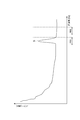
- FIG. 4 is a graph showing frequency characteristics of a detection signal for explaining a first setting example of a measurement frequency band and a reference frequency band in the semiconductor device inspection apparatus of FIG. 1.
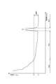
- 2 is a graph showing frequency characteristics of a detection signal for explaining a frequency region in which a reference frequency band can be set in the semiconductor device inspection apparatus of FIG. 1. It is a graph which shows the frequency characteristic of a detection signal in case system noise is superimposed on white noise.
- 2 is a semiconductor device image based on each of a measurement signal, a reference signal, and an analysis signal acquired by the semiconductor device inspection apparatus of FIG. 1.
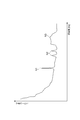
- 6 is a graph showing frequency characteristics of a detection signal for explaining a second setting example of a measurement frequency band and a reference frequency band in the semiconductor device inspection apparatus of FIG. 1.
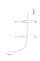
- 6 is a graph showing frequency characteristics of a detection signal for explaining a third setting example of a measurement frequency band and a reference frequency band in the semiconductor device inspection apparatus of FIG. 1.
- 8 is a semiconductor device image based on the analysis signal acquired by the semiconductor device inspection apparatus of FIG. 1 in the case of FIG. It is a block diagram of the semiconductor device test
- the semiconductor device inspection apparatus 1 is an apparatus for inspecting the semiconductor device 10 such as specifying an abnormality occurrence location in the semiconductor device 10 that is a device under test (DUT).
- the semiconductor device 10 includes an integrated circuit having a PN junction such as a transistor (for example, a small scale integrated circuit (SSI), a medium scale integrated circuit (MSI), a large scale integrated circuit (LSI: Large). Scale Integration), Very Large Scale Integration (VLSI), Ultra Large Scale Integration (ULSI), Giga Scale Integration (GSI), High Current / High Voltage There are MOS transistors and bipolar transistors.
- the semiconductor device 10 may be a semiconductor device that can be modulated by heat on a substrate.
- the semiconductor device inspection apparatus 1 includes a laser light source (light generation unit) 2.
- the laser light source 2 is operated by the first power source 3 and emits light irradiated on the semiconductor device 10.
- the light emitted from the laser light source 2 is guided to the scanning optical system 7 through the polarization-preserving single mode optical fiber 5 for probe light.
- the scan optical system 7 has a scan head 8 and a lens system 9. Thereby, the light guided to the scanning optical system 7 forms an image at a predetermined position of the semiconductor device 10, and the irradiation region of the light is scanned two-dimensionally with respect to the semiconductor device 10. Note that the scanning optical system 7 and the semiconductor device 10 are arranged in the dark box 6.
- the reflected light reflected by the semiconductor device 10 when the light emitted from the laser light source 2 is applied to the semiconductor device 10 is guided to the optical sensor (light detection unit) 12 through the optical fiber 11 for return light.
- the optical sensor 12 is operated by a second power source 13 provided separately from the first power source 3, and detects reflected light and outputs a detection signal.
- the detection signal output from the optical sensor 12 is input to the spectrum analyzer (signal generation unit) 15 via the amplifier 14.
- the spectrum analyzer 15 is electrically connected to the control device 18 via each of the frequency band setting unit 16 and the signal acquisition unit 17.
- the control device 18 forms a semiconductor device image based on the analysis signal acquired by the signal acquisition unit 17 and causes the display device 19 to display the semiconductor device image.
- a laser scan controller 21 is electrically connected to the control device 18.
- the laser scan controller 21 controls the laser light source 2 and the scan optical system 7.
- the spectrum analyzer 15 is electrically connected to a tester unit (electric signal applying unit) 22 including a tester, a pulse generator, and a power source.
- the tester unit 22 applies an electrical signal having a predetermined modulation frequency to the semiconductor device 10. Thereby, the semiconductor device 10 is driven at the time of inspection.
- the frequency band setting unit 16 sets a measurement frequency band FR1 and a reference frequency band FR2 for the detection signal input to the spectrum analyzer 15.
- the measurement frequency band FR1 is a frequency band including the frequency of the measurement signal S (N times (N is a natural number) the modulation frequency of the electric signal applied to the semiconductor device 10).
- the reference frequency band FR2 is a frequency band set in order to remove noise from the detection signal in the measurement frequency band FR1.
- the frequency band setting unit 16 calculates the level of the detection signal based on the power
- the level is equal to or lower than a level L2 obtained by adding 3 decibels to the reference white noise level L1.
- the reference white noise level L1 is a predetermined region (measurement region or measurement region) of the semiconductor device 10 in a state where the semiconductor device 10 is not driven (that is, a state where no electrical signal is input from the tester unit 22).
- This is a white noise level generated in the measurement frequency band FR1 when light is irradiated to the reference region and the reflected light reflected in the predetermined region is detected.
- the frequency band setting unit 16 does not need to detect the frequency region FD1 for setting the reference white noise level L1 and the reference frequency band FR2, and sets the reference frequency band FR2. Can be determined in advance. In the first example shown in FIG.
- the frequency band setting unit 16 sets the reference frequency band FR2 in the frequency region FD1 having a higher frequency than the measurement frequency band FR1. This is because, as shown in FIG. 3, there is a tendency that a frequency region FD2 in which 1 / F noise appears in a frequency region having a frequency lower than that of the measurement frequency band FR1.
- the spectrum analyzer 15 generates a measurement signal from the detection signal in the measurement frequency band FR1, and also generates a reference signal from the detection signal in the reference frequency band FR2.
- the spectrum analyzer 15 can simultaneously generate signals in a plurality of frequency bands.
- An example of such a spectrum analyzer is a cross domain analyzer manufactured by Advantest Corporation.
- the signal acquisition unit 17 acquires the analysis signal by calculating the difference between the measurement signal generated by the spectrum analyzer 15 and the reference signal. Thereby, an analysis signal from which shot noise, excess noise, and the like are removed can be acquired.
- S / N is a system noise related to the optical sensor 12 in addition to white noise such as shot noise of reflected light, excess noise of the laser light source 2 and thermal noise of the optical sensor 12, as shown in FIG. N1, system noise N2 related to the laser light source 2, and system noise N3 related to circuit operation, and the like.
- the shot noise is expressed as current noise i sn , and is expressed by the following equation, assuming that the charge of the electron is e, the photocurrent I D , the dark current I d , and the observed frequency band ⁇ f.
- excess noise is proportional to the amount of light, and its multiplier varies depending on the laser light source 2.
- shot noise and excess noise increase depending on the amount of reflected light. Specifically, shot noise is proportional to the square root of the amount of light, and excess noise is proportional to the amount of light.
- pattern image noise the semiconductor device image of FIG. An image similar to the semiconductor device image based on the signal (the semiconductor device image in FIG. 5A and corresponding to the semiconductor device image based on the measurement signal described above) is obtained.
- a signal in a predetermined frequency band is detected in the detection signal of the reflected light.
- the operating state of the semiconductor device can be detected by displaying the amplitude image, phase image, and IQ image obtained at this time on a display device.
- the image noise depending on the intensity of the reflected light from the surface of the semiconductor device is superimposed on the amplitude image signal as if it were a pattern image. Therefore, even if the signals are integrated for improving the S / N ratio of the image, the image noise is not lost and the signal is obscured.
- a generally used lock-in method an S / N improvement method by acquiring a frequency synchronized with a pulse train of a signal
- system noise such as system noise N1 related to the optical sensor 12, system noise N2 related to the laser light source 2, and system noise N3 related to circuit operation.
- system noise N1 and N2 caused by digital power sources such as a switching power source and a DD converter are removed by providing a first power source 3 for the laser light source 2 and a second power source 13 for the optical sensor 12 separately. is doing.
- the system noise N3 related to the circuit operation is removed by controlling the laser light source 2 and the optical sensor 12 from the outside without using an IC or the like used for controlling the laser light source 2 and the optical sensor 12 or the like.
- the range in which the measurement signal S exists is selected as the center frequency, and the bandwidth of the measurement frequency band FR1 is set directly or as a time constant.
- the bandwidth of the reference frequency band FR2 is set directly or as a time constant so that the center frequency is slightly shifted (for example, adjacent to each other continuously) so as to have the same bandwidth as the measurement frequency band FR1.
- the noise level when measuring with the same bandwidth or time constant is equivalent at a close frequency.
- the power at the frequency of the measurement frequency band FR1 is converted into amplitude energy. Further, the power at the frequency of the reference frequency band FR2 is also converted into amplitude energy. Then, if the difference between the converted amplitude energies is taken, it is possible to obtain the amplitude energy from which shot noise, excess noise and the like are removed.
- mapping based on this amplitude energy as shown in FIG. 5C, an optical signal map (corresponding to the above-described semiconductor device image based on the analysis signal) modulated by the response of the semiconductor device 10 is obtained. It can be obtained in real time.
- the semiconductor device 10 is irradiated with light, the reflected light reflected by the semiconductor device 10 is detected, and the detection signal is output.
- a frequency band setting step for setting the measurement frequency band FR1 and the reference frequency band FR2, a signal generation step for generating a measurement signal from the detection signal in the measurement frequency band FR1, and generating a reference signal from the detection signal in the reference frequency band FR2.
- a semiconductor device inspection method including a signal acquisition step of acquiring an analysis signal by calculating a difference between the measurement signal and the reference signal is performed.
- the level of the detection signal when the level of the detection signal is calculated based on the power, the level is referred to the frequency region FD1 where the level is equal to or lower than the level L2 obtained by adding 3 dB to the standard white noise level L1.
- the frequency band FR2 is set.
- the level of the detection signal when the level of the detection signal is calculated based on the amplitude energy, the level is equal to or lower than the level L2 obtained by adding 6 dB to the reference white noise level L1.
- the reference frequency band FR2 To the reference frequency band FR2.
- the measurement signal and the reference signal are generated based on the detection signal in the measurement frequency band FR1 and the detection signal in the reference frequency band FR2 detected at the same timing.
- the reference frequency band FR2 is set in the frequency region FD1 where the level is equal to or lower than the level L2 obtained by adding 3 dB to the standard white noise level L1. Is done.
- the analysis signal acquired by calculating the difference between the measurement signal and the reference signal is obtained by removing shot noise, excess noise, and the like.
- the measurement time can be shortened compared to the case where they are detected at different timings. be able to.
- the detection signal in the measurement frequency band FR1 and the detection signal in the reference frequency band FR2 are detected under the same conditions, the measurement results are more accurate than when they are detected under different conditions. Can be achieved.
- a sufficient signal strength exceeding the level L2 can be ensured by adjusting the band filter or the integration time (number of integrations) of the detection signal.
- the reference frequency band FR2 is set in a frequency region exceeding the level L2, not only the noise component but also the signal component disappears when the difference between the measurement signal and the reference signal is taken.
- the frequency band setting unit 16 sets the reference frequency band FR2 in the frequency region FD1 having a higher frequency than the measurement frequency band FR1. Thereby, it is possible to suppress the influence of the 1 / F noise that tends to appear in a relatively low frequency range from reaching the detection signal in the measurement frequency band FR1.
- the first power source 3 for the laser light source 2 and the second power source 13 for the optical sensor 12 are provided separately.
- a DD converter or the like that causes system noise, so that generation of system noise can be suppressed in the frequency region FD1 in which the reference frequency band FR2 is set.
- system noise is generated in the frequency domain FD1 in which the reference frequency band FR2 is set. This configuration is extremely important because it needs to be suppressed.
- a spectrum analyzer 15 that can simultaneously generate signals in a plurality of frequency bands is used. Accordingly, the measurement signal and the reference signal can be efficiently generated based on the detection signal in the measurement frequency band FR1 and the detection signal in the reference frequency band FR2 detected at the same timing.
- the measurement frequency band FR1 and the reference frequency band FR2 can be set as follows.
- the frequency characteristics of the detection signal can be displayed on the display device 19, and the user can manually set the frequency bands FR1 and FR2 while checking the screen. Further, it is possible to detect the power peak frequency, automatically set the measurement frequency band FR1 based on the detected peak frequency, and automatically set the reference frequency band FR2 within a range shifted by the set frequency. Further, the modulation frequency of the electrical signal applied to the semiconductor device 10 is acquired, and the measurement frequency band FR1 can be automatically set so as to include a frequency N times (N is a natural number) the modulation frequency. In that case, the measurement frequency band FR1 can be optimally set.
- the frequency dependent noise generated by the laser light source 2 can be obtained by measuring the light regularly reflected by a reference sample (mirror or the like). Moreover, when it measures without putting light, the frequency dependent noise produced by another apparatus can be acquired, and the frequency which generate
- the difference between the measurement signal and the reference signal may be calculated for each pixel or the entire screen.
- the measurement frequency band FR1 and the reference frequency band FR2 are set for each of the two frequencies, and the difference between the measurement signal and the reference signal is calculated for each of the two frequencies. While removing noise, excess noise, and the like, one signal can be displayed as positive with respect to the average and the other signal can be displayed as negative.
- FIG. 6 is a graph showing frequency characteristics of detection signals for explaining a second setting example of the measurement frequency band FR1 and the reference frequency band FR2.
- the frequency band setting unit 16 sets the frequency of the system noise N included in the measurement frequency band FR1.
- the reference frequency band FR2 is set so as to be included. That is, the measurement frequency band FR1 and the reference frequency band FR2 are set so that both of them include the system noise N. According to this, the system noise N can be removed from the analysis signal by calculating the difference between the measurement signal and the reference signal.
- This technique is particularly effective for samples in which a reference signal cannot be obtained, the base clock is unstable, and RBW must be wide.
- the measurement frequency band FR1 and the reference frequency band FR2 so as not to include the frequency of the system noise N. May be set.
- FIG. 7 is a graph showing frequency characteristics of detection signals for explaining a third setting example of the measurement frequency band FR1 and the reference frequency band FR2.
- the tester unit 22 has a first electric signal E1 having a first modulation frequency and a second electric signal E2 having a second modulation frequency different from the first modulation frequency (for example, for data
- the frequency band setting unit 16 uses the first modulation frequency and the second electric signal E2 of the first electric signal E1.
- the measurement frequency band FR1 and the reference frequency band FR2 are set based on the second modulation frequency.
- the measurement frequency band FR1 is set to include a frequency N times (N is a natural number) the first modulation frequency of the first electric signal E1, and the reference frequency band FR2 is the second modulation of the second electric signal E2.
- the frequency is set to include a frequency N times (N is a natural number).
- the light generation unit that generates light applied to the semiconductor device is not limited to the laser light source 2 and may be another light source such as a superluminescent diode.
- heat may be applied to the semiconductor device 10 instead of the electrical signal.
- the measurement frequency band FR1 is set to include a frequency N times (N is a natural number) the modulation frequency of heat applied to the semiconductor device 10.
- the semiconductor device inspection apparatus 1 replaces the spectrum analyzer 15 that can simultaneously generate signals in a plurality of frequency bands with the measurement signal from the detection signal in the measurement frequency band FR1.
- a first spectrum analyzer (signal generation unit) 15A to be generated and a second spectrum analyzer (signal generation unit) 15B to generate a reference signal from a detection signal in the reference frequency band FR2 may be provided.
- the detection signal output from the amplifier 14 is branched by the branch circuit 23 and input to the spectrum analyzers 15A and 15B.
- the semiconductor device inspection apparatus 1 replaces the spectrum analyzers 15A and 15B with a first lock-in amplifier (signal generation unit) 24A that generates a measurement signal from a detection signal in the measurement frequency band FR1, and a detection in the reference frequency band FR2.
- a second lock-in amplifier (signal generation unit) 24B that generates a reference signal from the signal.
- the measurement signal and the reference signal can be efficiently generated based on the detection signal in the measurement frequency band FR1 and the detection signal in the reference frequency band FR2 detected at the same timing.
- the reference frequency band FR2 is set to a frequency region that is not less than the maximum frequency of the frequency region FD2 in which 1 / F noise appears and not more than N times (N is a natural number) the modulation frequency of the electric signal applied to the semiconductor device 10. May be. Also in this case, the reference frequency band FR2 can be optimally set.
- SYMBOLS 1 ... Semiconductor device inspection apparatus, 2 ... Laser light source (light generation part), 3 ... 1st power supply, 10 ... Semiconductor device, 12 ... Optical sensor (light detection part), 13 ... 2nd power supply, 15 ... Spectrum analyzer (signal) Generation unit), 15A ... first spectrum analyzer (signal generation unit), 15B ... second spectrum analyzer (signal generation unit), 16 ... frequency band setting unit, 17 ... signal acquisition unit, 22 ... tester unit (electric signal application unit) ), 24A, first lock-in amplifier (signal generation unit), 24B, second lock-in amplifier (signal generation unit).
Landscapes
- Physics & Mathematics (AREA)
- Engineering & Computer Science (AREA)
- General Physics & Mathematics (AREA)
- Health & Medical Sciences (AREA)
- Computer Hardware Design (AREA)
- Microelectronics & Electronic Packaging (AREA)
- General Engineering & Computer Science (AREA)
- Computer Vision & Pattern Recognition (AREA)
- Electromagnetism (AREA)
- Toxicology (AREA)
- Life Sciences & Earth Sciences (AREA)
- Chemical & Material Sciences (AREA)
- Analytical Chemistry (AREA)
- Biochemistry (AREA)
- General Health & Medical Sciences (AREA)
- Immunology (AREA)
- Pathology (AREA)
- Tests Of Electronic Circuits (AREA)
- Investigating Or Analysing Materials By Optical Means (AREA)
- Testing Or Measuring Of Semiconductors Or The Like (AREA)
Abstract
半導体デバイス検査装置1は、光を出射するレーザ光源2と、当該光の半導体デバイス10での反射光を検出し、検出信号を出力する光センサ12と、検出信号に対して測定周波数帯域及び参照周波数帯域を設定する周波数帯域設定部16と、測定周波数帯域及び参照周波数帯域における検出信号から測定信号及び参照信号を生成するスペクトラムアナライザ15と、測定信号と参照信号との差分を算出することで、解析信号を取得する信号取得部17と、を備える。周波数帯域設定部16は、検出信号のレベルをパワーに基づいて算出した場合に、当該レベルが、基準となるホワイトノイズレベルに3デシベルを加算したレベル以下となる周波数領域に、参照周波数帯域を設定する。
Description
本発明は、半導体デバイス検査装置及び半導体デバイス検査方法に関する。
集積回路を検査する技術として、EOP(Electro Optical Probing)やEOFM(Electro-Optical Frequency Mapping)と称される光プロービング技術が知られている。光プロービング技術では、光源から出射された光を集積回路に照射し、集積回路で反射された反射光を光センサで検出して、検出信号を取得する。そして、取得した検出信号において、目的とする周波数を選び出し、その振幅エネルギーを時間的な経過として表示したり、2次元のマッピングとして表示したりする。これより、目的とした周波数で動作している回路の位置を特定することができる。
上述したような光プロービング技術では、反射光に含まれる変調信号が極めて少ないため、S/Nは、反射光のショットノイズ、光源の過剰雑音及び光センサのサーマルノイズ等に規定されてしまう。そのため、十分なS/Nを確保するためには、安定な光源を使用しつつスキャン時間を延ばしたり、光量を増やしたりする必要がある。
しかしながら、ショットノイズを根本的に除去することは不可能であり、ショットノイズ成分がパターン像として計測結果に重畳することは避けられない。しかも、計測結果には、光量の平方根に比例するショットノイズ成分に加え、光量に比例する過剰雑音成分も重畳する。したがって、単純なパターン像の画像処理でショットノイズ及び過剰雑音を除去することは困難である。
そこで、本発明は、計測時間の短縮化及び計測結果の高精度化を図ることができる半導体デバイス検査装置及び半導体デバイス検査方法を提供することを目的とする。
本発明の一側面に係る半導体デバイス検査装置は、被検査デバイスである半導体デバイスに照射される光を発生する光発生部と、光発生部が発生した光が半導体デバイスに照射されたときに半導体デバイスで反射された反射光を検出し、検出信号を出力する光検出部と、検出信号に対して測定周波数帯域及び参照周波数帯域を設定する周波数帯域設定部と、測定周波数帯域における検出信号から測定信号を生成し、参照周波数帯域における検出信号から参照信号を生成する信号生成部と、測定信号と参照信号との差分を算出することにより、解析信号を取得する信号取得部と、を備え、周波数帯域設定部は、検出信号のレベルをパワーに基づいて算出した場合に、当該レベルが、基準となるホワイトノイズレベルに3デシベルを加算したレベル以下となる周波数領域に、参照周波数帯域を設定する。
この半導体デバイス検査装置では、同一のタイミングで検出された測定周波数帯域における検出信号及び参照周波数帯域における検出信号に基づいて、測定信号及び参照信号が生成される。ここで、参照周波数帯域は、検出信号のレベルをパワーに基づいて算出した場合に、当該レベルが、基準となるホワイトノイズレベルに3デシベルを加算したレベル以下となる周波数領域に設定される。これにより、測定信号と参照信号との差分を算出することで取得された解析信号は、ショットノイズ及び過剰雑音等が除去されたものとなる。このように、測定周波数帯域における検出信号及び参照周波数帯域における検出信号が同一のタイミングで検出されるので、それらが別々のタイミングで検出される場合に比べ、計測時間の短時間化を図ることができる。しかも、測定周波数帯域における検出信号及び参照周波数帯域における検出信号が同一の条件下で検出されることになるので、それらが別々の条件下で検出される場合に比べ、計測結果の高精度化を図ることができる。
本発明の一側面に係る半導体デバイス検査装置では、周波数帯域設定部は、測定周波数帯域よりも周波数が高い周波数領域に、参照周波数帯域を設定してもよい。この構成によれば、比較的低い周波数領域に現れる傾向がある1/Fノイズの影響が測定周波数帯域における検出信号に及ぶのを抑制することができる。
本発明の一側面に係る半導体デバイス検査装置では、周波数帯域設定部は、測定周波数帯域に含まれるシステムノイズの周波数を含むように、参照周波数帯域を設定してもよい。この構成によれば、測定信号と参照信号との差分を算出することで、解析信号からシステムノイズを除去することができる。
本発明の一側面に係る半導体デバイス検査装置は、第1変調周波数を有する第1電気信号を半導体デバイスに印加する電気信号印加部を更に備え、周波数帯域設定部は、第1変調周波数の自然数倍の周波数を含むように、測定周波数帯域を設定してもよい。この構成によれば、測定周波数帯域の設定を最適に行うことができる。
本発明の一側面に係る半導体デバイス検査装置では、電気信号印加部は、第1変調周波数と異なる第2変調周波数を有する第2電気信号を第1電気信号と共に半導体デバイスに印加し、周波数帯域設定部は、第1変調周波数の自然数倍の周波数を含むように、測定周波数帯域を設定し、第2変調周波数の自然数倍の周波数を含むように、参照周波数帯域を設定してもよい。この構成によれば、測定周波数帯域に加え、参照周波数帯域においても、ショットノイズ及び過剰雑音等が除去された別の解析信号を取得することができる。
本発明の一側面に係る半導体デバイス検査装置は、光発生部を動作させる第1電源と、第1電源と別体で設けられ、光検出部を動作させる第2電源と、を更に備えてもよい。測定信号と参照信号との差分を算出することで、ショットノイズ及び過剰雑音等が除去された解析信号を取得するためには、参照周波数帯域が設定される周波数領域においてシステムノイズの発生を抑制する必要がある。そこで、第1電源と第2電源とを別体で設けることにより、システムノイズの発生要因となるDDコンバータ等を設けることが不要になるため、参照周波数帯域が設定される周波数領域においてシステムノイズの発生を抑制することができる。
本発明の一側面に係る半導体デバイス検査装置では、信号生成部は、測定周波数帯域における検出信号から測定信号を生成すると共に、参照周波数帯域における検出信号から参照信号を生成するスペクトラムアナライザを有してもよい。或いは、信号生成部は、測定周波数帯域における検出信号から測定信号を生成する第1ロックインアンプと、参照周波数帯域における検出信号から参照信号を生成する第2ロックインアンプと、を有してもよい。或いは、信号生成部は、測定周波数帯域における検出信号から測定信号を生成する第1スペクトラムアナライザと、参照周波数帯域における検出信号から参照信号を生成する第2スペクトラムアナライザと、を有してもよい。これらの構成によれば、同一のタイミングで検出された測定周波数帯域における検出信号及び参照周波数帯域における検出信号に基づいて、測定信号及び参照信号を効率良く生成することができる。
本発明の一側面に係る半導体デバイス検査装置は、被検査デバイスである半導体デバイスに照射される光を発生する光発生部と、光発生部が発生した光が半導体デバイスに照射されたときに半導体デバイスで反射された反射光を検出し、検出信号を出力する光検出部と、検出信号に対して測定周波数帯域及び参照周波数帯域を設定する周波数帯域設定部と、測定周波数帯域における検出信号から測定信号を生成し、参照周波数帯域における検出信号から参照信号を生成する信号生成部と、測定信号と参照信号との差分を算出することにより、解析信号を取得する信号取得部と、を備え、周波数帯域設定部は、検出信号のレベルを振幅エネルギーに基づいて算出した場合に、当該レベルが、基準となるホワイトノイズレベルに6デシベルを加算したレベル以下となる周波数領域に、参照周波数帯域を設定する。
本発明の一側面に係る半導体デバイス検査方法は、被検査デバイスである半導体デバイスに光を照射し、半導体デバイスで反射された反射光を検出して、検出信号を出力する光検出工程と、検出信号に対して測定周波数帯域及び参照周波数帯域を設定する周波数帯域設定工程と、測定周波数帯域における検出信号から測定信号を生成し、参照周波数帯域における検出信号から参照信号を生成する信号生成工程と、測定信号と参照信号との差分を算出することにより、解析信号を取得する信号取得工程と、を備え、周波数帯域設定工程では、検出信号のレベルをパワーに基づいて算出した場合に、当該レベルが、基準となるホワイトノイズレベルに3デシベルを加算したレベル以下となる周波数領域に、参照周波数帯域を設定する。
本発明の一側面に係る半導体デバイス検査方法は、被検査デバイスである半導体デバイスに光を照射し、半導体デバイスで反射された反射光を検出して、検出信号を出力する光検出工程と、検出信号に対して測定周波数帯域及び参照周波数帯域を設定する周波数帯域設定工程と、測定周波数帯域における検出信号から測定信号を生成し、参照周波数帯域における検出信号から参照信号を生成する信号生成工程と、測定信号と参照信号との差分を算出することにより、解析信号を取得する信号取得工程と、を備え、周波数帯域設定工程では、検出信号のレベルを振幅エネルギーに基づいて算出した場合に、当該レベルが、基準となるホワイトノイズレベルに6デシベルを加算したレベル以下となる周波数領域に、参照周波数帯域を設定する。
これらの半導体デバイス検査装置及び半導体デバイス検査方法によっても、上述した半導体デバイス検査装置と同様の理由により、計測時間の短縮化及び計測結果の高精度化を図ることができる。
本発明一側面に係るによれば、計測時間の短縮化及び計測結果の高精度化を図ることができる半導体デバイス検査装置及び半導体デバイス検査方法を提供することが可能となる。
以下、本発明の一実施形態について、図面を参照して詳細に説明する。なお、各図において同一又は相当部分には同一符号を付し、重複する説明を省略する。
図1に示されるように、半導体デバイス検査装置1は、被検査デバイス(DUT:Device Under Test)である半導体デバイス10において異常発生箇所を特定するなど、半導体デバイス10を検査するための装置である。半導体デバイス10としては、トランジスタ等のPNジャンクションを有する集積回路(例えば、小規模集積回路(SSI:Small Scale Integration)、中規模集積回路(MSI:Medium Scale Integration)、大規模集積回路(LSI:Large Scale Integration)、超大規模集積回路(VLSI:Very Large Scale Integration)、超々大規模集積回路(ULSI:Ultra Large Scale Integration)、ギガ・スケール集積回路(GSI:Giga Scale Integration))、大電流用/高圧用MOSトランジスタ及びバイポーラトランジスタ等がある。また、半導体デバイス10は、熱による変調を基板にかけられる半導体デバイスであってもよい。
半導体デバイス検査装置1は、レーザ光源(光発生部)2を備えている。レーザ光源2は、第1電源3によって動作させられ、半導体デバイス10に照射される光を出射する。レーザ光源2から出射された光は、プローブ光用の偏光保存シングルモード光ファイバ5を介して、スキャン光学系7に導光される。スキャン光学系7は、スキャンヘッド8及びレンズ系9を有している。これにより、スキャン光学系7に導光された光は、半導体デバイス10の所定位置に結像され、当該光の照射領域は、半導体デバイス10に対して2次元的に走査される。なお、スキャン光学系7及び半導体デバイス10は、暗箱6内に配置されている。
レーザ光源2から出射された光が半導体デバイス10に照射されたときに半導体デバイス10で反射された反射光は、戻り光用の光ファイバ11を介して、光センサ(光検出部)12に導光される。光センサ12は、第1電源3と別体で設けられた第2電源13によって動作させられ、反射光を検出して検出信号を出力する。光センサ12から出力された検出信号は、アンプ14を介して、スペクトラムアナライザ(信号生成部)15に入力される。スペクトラムアナライザ15は、周波数帯域設定部16及び信号取得部17のそれぞれを介して、制御装置18と電気的に接続されている。制御装置18は、信号取得部17によって取得された解析信号に基づいて半導体デバイス像を形成し、当該半導体デバイス像を表示装置19に表示させる。
制御装置18には、レーザスキャンコントローラ21が電気的に接続されている。レーザスキャンコントローラ21は、レーザ光源2及びスキャン光学系7を制御する。スペクトラムアナライザ15には、テスタ、パルスジェネレータ及び電源を含むテスタユニット(電気信号印加部)22が電気的に接続されている。テスタユニット22は、所定の変調周波数を有する電気信号を半導体デバイス10に印加する。これにより、半導体デバイス10は、検査時に駆動させられる。
次に、周波数帯域設定部16、スペクトラムアナライザ15及び信号取得部17について、より詳細に説明する。図2に示されるように、周波数帯域設定部16は、スペクトラムアナライザ15に入力された検出信号に対して測定周波数帯域FR1及び参照周波数帯域FR2を設定する。測定周波数帯域FR1は、測定信号Sの周波数(半導体デバイス10に印加する電気信号の変調周波数のN倍(Nは自然数)の周波数)を含む周波数帯域である。一方、参照周波数帯域FR2は、測定周波数帯域FR1における検出信号からノイズを除去するために設定される周波数帯域である。
図3に示されるように、周波数帯域設定部16は、検出信号のレベルをパワーに基づいて算出した場合に、当該レベルが、基準となるホワイトノイズレベルL1に3デシベルを加算したレベルL2以下となる周波数領域FD1に、参照周波数帯域FR2を設定する。これは、レベルL2がホワイトノイズレベルL1の約2倍であることを意味する(10log10L2-10log10L1=10log10(L2/L1)=3、L2≒L1×2)。なお、検出信号のレベルを振幅エネルギーに基づいて算出した場合には、基準となるホワイトノイズレベルL1に6デシベルを加算したレベルL2以下となる周波数領域FD1に、参照周波数帯域FR2を設定することになる(20log10L2-20log10L1=20log10(L2/L1)=6、L2≒L1×2)。
一例として、基準となるホワイトノイズレベルL1は、半導体デバイス10が駆動させられていない状態(すなわち、テスタユニット22から電気信号が入力されていない状態)で、半導体デバイス10の所定領域(計測領域又は参照領域)に光を照射し、当該所定領域で反射された反射光を検出した場合に、測定周波数帯域FR1に発生するホワイトノイズレベルである。なお、周波数帯域設定部16は、基準となるホワイトノイズレベルL1、及び参照周波数帯域FR2を設定するための周波数領域FD1を、計測の度に検出する必要はなく、参照周波数帯域FR2を設定する領域を予め決定しておくことができる。図2に示される第1例では、周波数帯域設定部16は、測定周波数帯域FR1よりも周波数が高い周波数領域FD1に、参照周波数帯域FR2を設定している。これは、図3に示されるように、測定周波数帯域FR1よりも周波数が低い周波数領域に、1/Fノイズが現れる周波数領域FD2が存在する傾向があるからである。
スペクトラムアナライザ15は、測定周波数帯域FR1における検出信号から測定信号を生成すると共に、参照周波数帯域FR2における検出信号から参照信号を生成する。このように、スペクトラムアナライザ15は、複数の周波数帯域における信号の生成を同時に実施することができるものである。このようなスペクトラムアナライザとしては、例えば、アドバンテスト社のクロス・ドメイン・アナライザがある。信号取得部17は、スペクトラムアナライザ15によって生成された測定信号と参照信号との差分を算出することにより、解析信号を取得する。これにより、ショットノイズ及び過剰雑音等が除去された解析信号を取得することができる。
次に、信号取得部17におけるノイズの除去について、より詳細に説明する。光プロービング技術において、S/Nは、図4に示されるように、反射光のショットノイズ、レーザ光源2の過剰雑音及び光センサ12のサーマルノイズ等のホワイトノイズに加え、光センサ12に関するシステムノイズN1、レーザ光源2に関するシステムノイズN2、及び回路動作に関するシステムノイズN3等のシステムノイズによって規定される。
ショットノイズは、電流ノイズisnとして示され、電子の電荷e、光電流ID、ダーク電流Id、観察する周波数帯Δfとすると、次式で表される。これに対し、過剰雑音は、光の光量に比例し、その乗数は、レーザ光源2により様々である。

光プロービング技術において、ショットノイズ及び過剰雑音は、反射光の光量に依存して増加する。具体的には、ショットノイズは光量の平方根に比例し、過剰雑音は光量に比例する。その結果、ノイズ成分が重畳された状態でマッピングすると、図5の(a),(b)に示されるように、パターン像ノイズ(図5の(b)の半導体デバイス像であり、上述した参照信号に基づく半導体デバイス像に相当する)に類似する画像(図5の(a)の半導体デバイス像であり、上述した測定信号に基づく半導体デバイス像に相当する)が得られる。
ここで、ショットノイズを根本的に除去することは不可能であり、ショットノイズ成分がパターン像として計測結果に重畳することは避けられない。しかも、計測結果には、光量の平方根に比例するショットノイズ成分に加え、光量に比例する過剰雑音成分も重畳する。したがって、単純なパターン像の画像処理でショットノイズ及び過剰雑音を除去することは困難である。
そこで、既存の光プロービング技術では、反射光の検出信号において、所定周波数帯域の信号を検出する。このとき得られた振幅像、位相像及びIQ像を表示装置に表示することにより、半導体デバイスの動作状態を検出することができる。ところが、振幅像の信号には、上述したように、半導体デバイスの表面からの反射光の強度に依存した画像ノイズが、あたかもパターン像のように重畳してしまう。そのため、画像のS/N向上のために信号を積算しても、画像ノイズが消えることはなく、信号を覆い隠してしまう。なお、一般によく用いられるロックイン法(信号のパルス列に対して同期した周波数を取得することによるS/N向上手法)は、ここまでの方法と同じことである。
上述した半導体デバイス検査装置1によれば、上記問題を解決することができる。まず、光センサ12に関するシステムノイズN1、レーザ光源2に関するシステムノイズN2、及び回路動作に関するシステムノイズN3等のシステムノイズ(図4参照)を除去する必要がある。そのために、レーザ光源2用の第1電源3と光センサ12用の第2電源13とを別体で設けることで、スイッチング電源及びDDコンバータ等のデジタル電源に起因するシステムノイズN1,N2を除去している。また、レーザ光源2及び光センサ12等の制御に用いるIC等を使用せず、レーザ光源2及び光センサ12等を外部から制御することで、回路動作に関するシステムノイズN3を除去している。
そして、計測の際には、測定信号Sの存在する範囲を中心周波数として選択し、直接又は時定数として測定周波数帯域FR1のバンド幅を設定する。また、中心周波数をわずかにずらしたところに(例えば、連続して隣り合うところに)、測定周波数帯域FR1と同じバンド幅を有するように、直接又は時定数として参照周波数帯域FR2のバンド幅を設定する。特に周波数に依存するノイズがない場合には、同じバンド幅又は時定数で計測する際のノイズレベルは近い周波数で同等になる。
続いて、測定周波数帯域FR1の周波数におけるパワーを振幅エネルギーに換算する。また、参照周波数帯域FR2の周波数におけるパワーも振幅エネルギーに変換する。そして、変換された振幅エネルギー同士の差分をとると、ショットノイズ及び過剰雑音等が除去された振幅エネルギーを取得することができる。この振幅エネルギーを基にマッピングすることで、図5の(c)に示されるように、半導体デバイス10の応答によって変調された光信号マップ(上述した解析信号に基づく半導体デバイス像に相当する)をリアルタイムに得ることができる。
以上説明したように、半導体デバイス検査装置1では、半導体デバイス10に光を照射し、半導体デバイス10で反射された反射光を検出して、検出信号を出力する光検出工程と、検出信号に対して測定周波数帯域FR1及び参照周波数帯域FR2を設定する周波数帯域設定工程と、測定周波数帯域FR1における検出信号から測定信号を生成し、参照周波数帯域FR2における検出信号から参照信号を生成する信号生成工程と、測定信号と参照信号との差分を算出することにより、解析信号を取得する信号取得工程と、を備える半導体デバイス検査方法が実施される。そして、周波数帯域設定工程では、検出信号のレベルをパワーに基づいて算出した場合に、当該レベルが、基準となるホワイトノイズレベルL1に3デシベルを加算したレベルL2以下となる周波数領域FD1に、参照周波数帯域FR2を設定する。換言すれば、周波数帯域設定工程では、検出信号のレベルを振幅エネルギーに基づいて算出した場合に、当該レベルが、基準となるホワイトノイズレベルL1に6デシベルを加算したレベルL2以下となる周波数領域FD1に、参照周波数帯域FR2を設定する。
このように、半導体デバイス検査装置1では、同一のタイミングで検出された測定周波数帯域FR1における検出信号及び参照周波数帯域FR2における検出信号に基づいて、測定信号及び参照信号が生成される。ここで、参照周波数帯域FR2は、検出信号のレベルをパワーに基づいて算出した場合に、当該レベルが、基準となるホワイトノイズレベルL1に3デシベルを加算したレベルL2以下となる周波数領域FD1に設定される。これにより、測定信号と参照信号との差分を算出することで取得された解析信号は、ショットノイズ及び過剰雑音等が除去されたものとなる。このように、測定周波数帯域FR1における検出信号及び参照周波数帯域FR2における検出信号が同一のタイミングで検出されるので、それらが別々のタイミングで検出される場合に比べ、計測時間の短時間化を図ることができる。しかも、測定周波数帯域FR1における検出信号及び参照周波数帯域FR2における検出信号が同一の条件下で検出されることになるので、それらが別々の条件下で検出される場合に比べ、計測結果の高精度化を図ることができる。
なお、帯域フィルタ又は検出信号の積算時間(積算回数)を調整することで、測定信号がレベルL2を超える十分な信号強度を確保することができる。ただし、レベルL2を超える周波数領域に参照周波数帯域FR2を設定すると、測定信号と参照信号との差分をとったときに、ノイズ成分だけでなく信号成分が消えてしまうことになる。
また、半導体デバイス検査装置1では、周波数帯域設定部16が、測定周波数帯域FR1よりも周波数が高い周波数領域FD1に、参照周波数帯域FR2を設定する。これにより、比較的低い周波数領域に現れる傾向がある1/Fノイズの影響が測定周波数帯域FR1における検出信号に及ぶのを抑制することができる。
また、半導体デバイス検査装置1では、レーザ光源2用の第1電源3と光センサ12用の第2電源13とが別体で設けられている。これにより、システムノイズの発生要因となるDDコンバータ等を設けることが不要になるため、参照周波数帯域FR2が設定される周波数領域FD1においてシステムノイズの発生を抑制することができる。測定信号と参照信号との差分を算出することで、ショットノイズ及び過剰雑音等が除去された解析信号を取得するためには、参照周波数帯域FR2が設定される周波数領域FD1においてシステムノイズの発生を抑制することが必要であることから、この構成は、極めて重要である。
また、半導体デバイス検査装置1では、複数の周波数帯域における信号の生成を同時に実施することができるスペクトラムアナライザ15が用いられている。これにより、同一のタイミングで検出された測定周波数帯域FR1における検出信号及び参照周波数帯域FR2における検出信号に基づいて、測定信号及び参照信号を効率良く生成することができる。
なお、測定周波数帯域FR1及び参照周波数帯域FR2の設定は、次のように行うことができる。例えば、表示装置19に検出信号の周波数特性を表示させ、ユーザが画面を確認しながら各周波数帯域FR1,FR2を手動で設定することができる。また、パワーのピーク周波数を検出し、それを基に測定周波数帯域FR1を自動で設定し、設定された周波数の分だけずれた範囲に参照周波数帯域FR2を自動で設定することができる。また、半導体デバイス10に印加する電気信号の変調周波数を取得し、その変調周波数のN倍(Nは自然数)の周波数を含むように、測定周波数帯域FR1を自動で設定することができる。その場合、測定周波数帯域FR1の設定を最適に行うことができる。
また、レーザ光源2によって生じる周波数依存ノイズは、リファレンスサンプル(鏡等)で正反射した光を計測することで、発生する周波数を取得することができる。また、光を入れずに計測した場合、その他の装置によって生じる周波数依存ノイズを取得することができ、それにより、発生する周波数を取得することができる。
また、測定信号と参照信号との差分の算出は、ピクセルごとに行ってもよいし、画面全体で行ってもよい。また、2つの周波数を同時に観察したい場合には、当該2つの周波数のそれぞれに測定周波数帯域FR1及び参照周波数帯域FR2を設定し、それらについて測定信号と参照信号との差分の算出することにより、ショットノイズ及び過剰雑音等が除去しつつ、平均に対して一方の信号を正として表示すると共に他方の信号を負として表示することができる。
図6は、測定周波数帯域FR1及び参照周波数帯域FR2の第2設定例を説明するための検出信号の周波数特性を示すグラフである。図6に示されるように、例えば、除去しきれないシステムノイズNが測定信号Sの近傍に存在する場合には、周波数帯域設定部16は、測定周波数帯域FR1に含まれるシステムノイズNの周波数を含むように、参照周波数帯域FR2を設定する。すなわち、測定周波数帯域FR1及び参照周波数帯域FR2は、それらの両方がシステムノイズNを含むように設定される。これによれば、測定信号と参照信号との差分を算出することで、解析信号からシステムノイズNを除去することができる。本手法は、特に、リファレンス信号が得られず、ベースクロックが不安定で、RBWを広くとらなくてはならないサンプルの際に有効となる。なお、例えば、除去しきれないシステムノイズNの周波数に対して測定信号Sの周波数をシフトさせることができる場合には、システムノイズNの周波数を含まないように測定周波数帯域FR1及び参照周波数帯域FR2を設定してもよい。
図7は、測定周波数帯域FR1及び参照周波数帯域FR2の第3設定例を説明するための検出信号の周波数特性を示すグラフである。図7に示されるように、例えば、テスタユニット22が、第1変調周波数を有する第1電気信号E1、及び第1変調周波数と異なる第2変調周波数を有する第2電気信号E2(例えば、データ用フリップフロップ及びクロックバッファ)を半導体デバイス10に印加する場合において、それらの信号による変調を同時に観察したいときには、周波数帯域設定部16は、第1電気信号E1の第1変調周波数及び第2電気信号E2の第2変調周波数に基づいて、測定周波数帯域FR1及び参照周波数帯域FR2を設定する。すなわち、測定周波数帯域FR1は、第1電気信号E1の第1変調周波数のN倍(Nは自然数)の周波数を含むように設定され、参照周波数帯域FR2は、第2電気信号E2の第2変調周波数のN倍(Nは自然数)の周波数を含むように設定される。これによれば、測定周波数帯域FR1に基づく測定信号S1と参照周波数帯域FR2に基づく測定信号S2との差分を算出することで、測定周波数帯域FR1に加え、参照周波数帯域FR2においても、ショットノイズ及び過剰雑音等が除去された別の解析信号を取得することができる。そして、図8に示されるように、測定信号S1に対応する領域を白、測定信号S2に対応する領域を黒というように、色分けされた半導体デバイス像を得ることができる。
以上、本発明の一実施形態について説明したが、本発明は、上記実施形態に限定されるものではない。例えば、半導体デバイスに照射される光を発生する光発生部は、レーザ光源2に限定されず、スーパールミネッセントダイオード等の他の光源であってもよい。また、半導体デバイス10に対し、電気信号に代えて、熱を印加してもよい。その場合、測定周波数帯域FR1は、半導体デバイス10に印加する熱の変調周波数のN倍(Nは自然数)の周波数を含むように設定される。また、図9に示されるように、半導体デバイス検査装置1は、複数の周波数帯域における信号の生成を同時に実施することができるスペクトラムアナライザ15に代えて、測定周波数帯域FR1における検出信号から測定信号を生成する第1スペクトラムアナライザ(信号生成部)15Aと、参照周波数帯域FR2における検出信号から参照信号を生成する第2スペクトラムアナライザ(信号生成部)15Bと、を備えるものであってもよい。その場合には、アンプ14から出力された検出信号は、分岐回路23によって分岐され、各スペクトラムアナライザ15A,15Bに入力される。更に、半導体デバイス検査装置1は、スペクトラムアナライザ15A,15Bに代えて、測定周波数帯域FR1における検出信号から測定信号を生成する第1ロックインアンプ(信号生成部)24Aと、参照周波数帯域FR2における検出信号から参照信号を生成する第2ロックインアンプ(信号生成部)24Bと、を備えるものであってもよい。いずれの構成によっても、同一のタイミングで検出された測定周波数帯域FR1における検出信号及び参照周波数帯域FR2における検出信号に基づいて、測定信号及び参照信号を効率良く生成することができる。また、参照周波数帯域FR2は、1/Fノイズが現れる周波数領域FD2の最大周波数以上且つ半導体デバイス10に印加する電気信号の変調周波数のN倍(Nは自然数)の周波数以下の周波数領域に設定されてもよい。この場合にも、参照周波数帯域FR2の設定を最適に行うことができる。
1…半導体デバイス検査装置、2…レーザ光源(光発生部)、3…第1電源、10…半導体デバイス、12…光センサ(光検出部)、13…第2電源、15…スペクトラムアナライザ(信号生成部)、15A…第1スペクトラムアナライザ(信号生成部)、15B…第2スペクトラムアナライザ(信号生成部)、16…周波数帯域設定部、17…信号取得部、22…テスタユニット(電気信号印加部)、24A…第1ロックインアンプ(信号生成部)、24B…第2ロックインアンプ(信号生成部)。
Claims (12)
- 被検査デバイスである半導体デバイスに照射される光を発生する光発生部と、
前記光発生部が発生した前記光が前記半導体デバイスに照射されたときに前記半導体デバイスで反射された反射光を検出し、検出信号を出力する光検出部と、
前記検出信号に対して測定周波数帯域及び参照周波数帯域を設定する周波数帯域設定部と、
前記測定周波数帯域における前記検出信号から測定信号を生成し、前記参照周波数帯域における前記検出信号から参照信号を生成する信号生成部と、
前記測定信号と前記参照信号との差分を算出することにより、解析信号を取得する信号取得部と、を備え、
前記周波数帯域設定部は、前記検出信号のレベルをパワーに基づいて算出した場合に、当該レベルが、基準となるホワイトノイズレベルに3デシベルを加算したレベル以下となる周波数領域に、前記参照周波数帯域を設定する、半導体デバイス検査装置。 - 前記周波数帯域設定部は、前記測定周波数帯域よりも周波数が高い前記周波数領域に、前記参照周波数帯域を設定する、請求項1記載の半導体デバイス検査装置。
- 前記周波数帯域設定部は、前記測定周波数帯域に含まれるシステムノイズの周波数を含むように、前記参照周波数帯域を設定する、請求項1記載の半導体デバイス検査装置。
- 第1変調周波数を有する第1電気信号を前記半導体デバイスに印加する電気信号印加部を更に備え、
前記周波数帯域設定部は、前記第1変調周波数の自然数倍の周波数を含むように、前記測定周波数帯域を設定する、請求項1記載の半導体デバイス検査装置。 - 前記電気信号印加部は、前記第1変調周波数と異なる第2変調周波数を有する第2電気信号を前記第1電気信号と共に前記半導体デバイスに印加し、
前記周波数帯域設定部は、前記第1変調周波数の自然数倍の周波数を含むように、前記測定周波数帯域を設定し、前記第2変調周波数の自然数倍の周波数を含むように、前記参照周波数帯域を設定する、請求項4記載の半導体デバイス検査装置。 - 前記光発生部を動作させる第1電源と、
前記第1電源と別体で設けられ、前記光検出部を動作させる第2電源と、を更に備える、請求項1~5のいずれか一項記載の半導体デバイス検査装置。 - 前記信号生成部は、前記測定周波数帯域における前記検出信号から前記測定信号を生成すると共に、前記参照周波数帯域における前記検出信号から前記参照信号を生成するスペクトラムアナライザを有する、請求項1~6のいずれか一項記載の半導体デバイス検査装置。
- 前記信号生成部は、前記測定周波数帯域における前記検出信号から前記測定信号を生成する第1ロックインアンプと、前記参照周波数帯域における前記検出信号から前記参照信号を生成する第2ロックインアンプと、を有する、請求項1~6のいずれか一項記載の半導体デバイス検査装置。
- 前記信号生成部は、前記測定周波数帯域における前記検出信号から前記測定信号を生成する第1スペクトラムアナライザと、前記参照周波数帯域における前記検出信号から前記参照信号を生成する第2スペクトラムアナライザと、を有する、請求項1~6のいずれか一項記載の半導体デバイス検査装置。
- 被検査デバイスである半導体デバイスに照射される光を発生する光発生部と、
前記光発生部が発生した前記光が前記半導体デバイスに照射されたときに前記半導体デバイスで反射された反射光を検出し、検出信号を出力する光検出部と、
前記検出信号に対して測定周波数帯域及び参照周波数帯域を設定する周波数帯域設定部と、
前記測定周波数帯域における前記検出信号から測定信号を生成し、前記参照周波数帯域における前記検出信号から参照信号を生成する信号生成部と、
前記測定信号と前記参照信号との差分を算出することにより、解析信号を取得する信号取得部と、を備え、
前記周波数帯域設定部は、前記検出信号のレベルを振幅エネルギーに基づいて算出した場合に、当該レベルが、基準となるホワイトノイズレベルに6デシベルを加算したレベル以下となる周波数領域に、前記参照周波数帯域を設定する、半導体デバイス検査装置。 - 被検査デバイスである半導体デバイスに光を照射し、前記半導体デバイスで反射された反射光を検出して、検出信号を出力する光検出工程と、
前記検出信号に対して測定周波数帯域及び参照周波数帯域を設定する周波数帯域設定工程と、
前記測定周波数帯域における前記検出信号から測定信号を生成し、前記参照周波数帯域における前記検出信号から参照信号を生成する信号生成工程と、
前記測定信号と前記参照信号との差分を算出することにより、解析信号を取得する信号取得工程と、を備え、
前記周波数帯域設定工程では、前記検出信号のレベルをパワーに基づいて算出した場合に、当該レベルが、基準となるホワイトノイズレベルに3デシベルを加算したレベル以下となる周波数領域に、前記参照周波数帯域を設定する、半導体デバイス検査方法。 - 被検査デバイスである半導体デバイスに光を照射し、前記半導体デバイスで反射された反射光を検出して、検出信号を出力する光検出工程と、
前記検出信号に対して測定周波数帯域及び参照周波数帯域を設定する周波数帯域設定工程と、
前記測定周波数帯域における前記検出信号から測定信号を生成し、前記参照周波数帯域における前記検出信号から参照信号を生成する信号生成工程と、
前記測定信号と前記参照信号との差分を算出することにより、解析信号を取得する信号取得工程と、を備え、
前記周波数帯域設定工程では、前記検出信号のレベルを振幅エネルギーに基づいて算出した場合に、当該レベルが、基準となるホワイトノイズレベルに6デシベルを加算したレベル以下となる周波数領域に、前記参照周波数帯域を設定する、半導体デバイス検査方法。
Priority Applications (3)
| Application Number | Priority Date | Filing Date | Title |
|---|---|---|---|
| US14/440,175 US9588175B2 (en) | 2012-11-06 | 2013-10-25 | Semiconductor device inspection device and semiconductor device inspection method |
| US15/400,064 US10060975B2 (en) | 2012-11-06 | 2017-01-06 | Semiconductor device inspection device and semiconductor device inspection method |
| US16/030,233 US10705139B2 (en) | 2012-11-06 | 2018-07-09 | Semiconductor device inspection device and semiconductor device inspection method |
Applications Claiming Priority (2)
| Application Number | Priority Date | Filing Date | Title |
|---|---|---|---|
| JP2012-244636 | 2012-11-06 | ||
| JP2012244636A JP6166032B2 (ja) | 2012-11-06 | 2012-11-06 | 半導体デバイス検査装置及び半導体デバイス検査方法 |
Related Child Applications (2)
| Application Number | Title | Priority Date | Filing Date |
|---|---|---|---|
| US14/440,175 A-371-Of-International US9588175B2 (en) | 2012-11-06 | 2013-10-25 | Semiconductor device inspection device and semiconductor device inspection method |
| US15/400,064 Continuation US10060975B2 (en) | 2012-11-06 | 2017-01-06 | Semiconductor device inspection device and semiconductor device inspection method |
Publications (1)
| Publication Number | Publication Date |
|---|---|
| WO2014073398A1 true WO2014073398A1 (ja) | 2014-05-15 |
Family
ID=50684508
Family Applications (1)
| Application Number | Title | Priority Date | Filing Date |
|---|---|---|---|
| PCT/JP2013/078987 Ceased WO2014073398A1 (ja) | 2012-11-06 | 2013-10-25 | 半導体デバイス検査装置及び半導体デバイス検査方法 |
Country Status (4)
| Country | Link |
|---|---|
| US (3) | US9588175B2 (ja) |
| JP (1) | JP6166032B2 (ja) |
| TW (1) | TWI595227B (ja) |
| WO (1) | WO2014073398A1 (ja) |
Families Citing this family (10)
| Publication number | Priority date | Publication date | Assignee | Title |
|---|---|---|---|---|
| WO2014119676A1 (ja) * | 2013-02-01 | 2014-08-07 | 浜松ホトニクス株式会社 | 半導体デバイス検査装置及び半導体デバイス検査方法 |
| JP6283501B2 (ja) | 2013-11-12 | 2018-02-21 | 浜松ホトニクス株式会社 | 周波数解析装置及び周波数解析方法 |
| JP6283507B2 (ja) | 2013-11-29 | 2018-02-21 | 浜松ホトニクス株式会社 | 半導体デバイス計測装置及び半導体デバイス計測方法 |
| JP6391370B2 (ja) * | 2014-08-29 | 2018-09-19 | キヤノン株式会社 | 光ポンピング磁力計及び磁気センシング方法 |
| TWI627418B (zh) * | 2016-05-13 | 2018-06-21 | 南韓商英泰克普拉斯有限公司 | 半導體元件檢查裝置 |
| JP6714485B2 (ja) | 2016-09-28 | 2020-06-24 | 浜松ホトニクス株式会社 | 半導体デバイス検査方法及び半導体デバイス検査装置 |
| WO2019131410A1 (ja) | 2017-12-27 | 2019-07-04 | 株式会社Photo electron Soul | 試料検査装置、および、試料検査方法 |
| JP6611387B1 (ja) * | 2018-08-30 | 2019-11-27 | 浜松ホトニクス株式会社 | 半導体試料の検査装置及び検査方法 |
| JP7554052B2 (ja) | 2020-01-31 | 2024-09-19 | 浜松ホトニクス株式会社 | 半導体故障解析装置 |
| KR102773941B1 (ko) | 2020-02-18 | 2025-02-27 | 하마마츠 포토닉스 가부시키가이샤 | 반도체 고장 해석 장치 및 반도체 고장 해석 방법 |
Citations (3)
| Publication number | Priority date | Publication date | Assignee | Title |
|---|---|---|---|---|
| JPH01169862A (ja) * | 1987-12-25 | 1989-07-05 | Hitachi Ltd | 荷電粒子線装置 |
| JPH07260891A (ja) * | 1994-03-18 | 1995-10-13 | Fujitsu Ltd | 電圧測定方法及び装置 |
| WO2006011423A1 (ja) * | 2004-07-28 | 2006-02-02 | Matsushita Electric Industrial Co., Ltd. | 受信装置 |
Family Cites Families (26)
| Publication number | Priority date | Publication date | Assignee | Title |
|---|---|---|---|---|
| JPH0769364B2 (ja) * | 1987-03-06 | 1995-07-31 | アンリツ株式会社 | スペクトラムアナライザ |
| JP3352543B2 (ja) * | 1994-09-29 | 2002-12-03 | 浜松ホトニクス株式会社 | 電圧測定装置 |
| JPH1084250A (ja) * | 1996-09-09 | 1998-03-31 | Omron Corp | ノイズ除去フィルタ |
| JPH11133118A (ja) * | 1997-10-29 | 1999-05-21 | Hamamatsu Photonics Kk | 基板検査装置 |
| WO2000079248A1 (fr) * | 1999-06-21 | 2000-12-28 | Hamamatsu Photonics K.K. | Spectrometre a ondes terahertz |
| US6252222B1 (en) | 2000-01-13 | 2001-06-26 | Schlumberger Technologies, Inc. | Differential pulsed laser beam probing of integrated circuits |
| US6478625B2 (en) * | 2000-07-11 | 2002-11-12 | Bernard R. Tolmie | Electrical-optical hybrid connector |
| JP2004144685A (ja) * | 2002-10-28 | 2004-05-20 | Hitachi Ltd | 半導体デバイス製造ラインにおける外観検査装置の機差調整方法及びそのシステム |
| JP4516294B2 (ja) * | 2003-09-30 | 2010-08-04 | パナソニック株式会社 | 半導体装置及び半導体装置の製造方法 |
| EP1743576B1 (en) * | 2004-05-06 | 2018-01-24 | Nippon Telegraph And Telephone Corporation | Component concentration measuring device and method of controlling component concentration measuring device |
| JP4578942B2 (ja) * | 2004-11-10 | 2010-11-10 | オリンパス株式会社 | 内視鏡形状検出装置 |
| US7659981B2 (en) | 2005-08-26 | 2010-02-09 | Dcg Systems, Inc. | Apparatus and method for probing integrated circuits using polarization difference probing |
| JP3784823B1 (ja) * | 2005-07-15 | 2006-06-14 | 国立大学法人徳島大学 | 距離測定装置、距離測定方法および距離測定プログラム |
| US7733100B2 (en) * | 2005-08-26 | 2010-06-08 | Dcg Systems, Inc. | System and method for modulation mapping |
| TW200717682A (en) | 2005-10-11 | 2007-05-01 | Orbotech Ltd | Method for inspecting microelectronic components on a substrate and apparatus for testing same |
| JP4420051B2 (ja) * | 2007-03-28 | 2010-02-24 | ソニー株式会社 | レーザ光発生装置 |
| US20100158189A1 (en) | 2007-05-15 | 2010-06-24 | Hamamatsu Foundation For Science And Technology Promotion | Mossbauer spectrometer |
| WO2009028063A1 (ja) * | 2007-08-30 | 2009-03-05 | Mitsui Engineering & Shipbuilding Co., Ltd. | Fret検出方法及び装置 |
| JP5187843B2 (ja) * | 2008-09-01 | 2013-04-24 | 浜松ホトニクス株式会社 | 半導体検査装置及び検査方法 |
| JP4564567B2 (ja) * | 2009-02-13 | 2010-10-20 | 三井造船株式会社 | 蛍光検出装置及び蛍光検出方法 |
| SG10201401887YA (en) | 2009-05-01 | 2014-06-27 | Dcg Systems Inc | Systems and method for laser voltage imaging state mapping |
| JP2012008261A (ja) * | 2010-06-23 | 2012-01-12 | Hamamatsu Photonics Kk | 画像生成装置 |
| JP5429494B2 (ja) * | 2010-07-20 | 2014-02-26 | 横河電機株式会社 | 多チャンネル測光測定装置 |
| US9279723B2 (en) * | 2010-08-19 | 2016-03-08 | Novatrans Group Sa | Terahertz spectroscopy system and method |
| JP5595883B2 (ja) * | 2010-11-29 | 2014-09-24 | 株式会社東芝 | 無線通信装置 |
| EP2816388A4 (en) * | 2012-02-15 | 2015-07-22 | Olympus Corp | LASER SCANNING TYPE VISUALIZATION DEVICE |
-
2012
- 2012-11-06 JP JP2012244636A patent/JP6166032B2/ja active Active
-
2013
- 2013-10-25 US US14/440,175 patent/US9588175B2/en active Active
- 2013-10-25 WO PCT/JP2013/078987 patent/WO2014073398A1/ja not_active Ceased
- 2013-11-06 TW TW102140334A patent/TWI595227B/zh active
-
2017
- 2017-01-06 US US15/400,064 patent/US10060975B2/en active Active
-
2018
- 2018-07-09 US US16/030,233 patent/US10705139B2/en active Active
Patent Citations (3)
| Publication number | Priority date | Publication date | Assignee | Title |
|---|---|---|---|---|
| JPH01169862A (ja) * | 1987-12-25 | 1989-07-05 | Hitachi Ltd | 荷電粒子線装置 |
| JPH07260891A (ja) * | 1994-03-18 | 1995-10-13 | Fujitsu Ltd | 電圧測定方法及び装置 |
| WO2006011423A1 (ja) * | 2004-07-28 | 2006-02-02 | Matsushita Electric Industrial Co., Ltd. | 受信装置 |
Also Published As
| Publication number | Publication date |
|---|---|
| JP6166032B2 (ja) | 2017-07-19 |
| US20170123003A1 (en) | 2017-05-04 |
| TWI595227B (zh) | 2017-08-11 |
| US10060975B2 (en) | 2018-08-28 |
| JP2014092514A (ja) | 2014-05-19 |
| US20150276865A1 (en) | 2015-10-01 |
| TW201428264A (zh) | 2014-07-16 |
| US9588175B2 (en) | 2017-03-07 |
| US10705139B2 (en) | 2020-07-07 |
| US20180348297A1 (en) | 2018-12-06 |
Similar Documents
| Publication | Publication Date | Title |
|---|---|---|
| JP6166032B2 (ja) | 半導体デバイス検査装置及び半導体デバイス検査方法 | |
| US10191104B2 (en) | Semiconductor device inspection device and semiconductor device inspection method | |
| KR102270039B1 (ko) | 반도체 디바이스 테스트 장치 및 반도체 디바이스 테스트 방법 | |
| US9618550B2 (en) | Apparatus for frequency analyzing a measurement target and method of frequency analyzing a measurement target | |
| JP6824351B1 (ja) | 半導体試料の検査装置及び検査方法 | |
| US10139447B2 (en) | Image generation apparatus and image generation method |
Legal Events
| Date | Code | Title | Description |
|---|---|---|---|
| 121 | Ep: the epo has been informed by wipo that ep was designated in this application |
Ref document number: 13853710 Country of ref document: EP Kind code of ref document: A1 |
|
| WWE | Wipo information: entry into national phase |
Ref document number: 14440175 Country of ref document: US |
|
| NENP | Non-entry into the national phase |
Ref country code: DE |
|
| 122 | Ep: pct application non-entry in european phase |
Ref document number: 13853710 Country of ref document: EP Kind code of ref document: A1 |