WO2014069032A1 - 電界効果型半導体装置及びその製造方法 - Google Patents
電界効果型半導体装置及びその製造方法 Download PDFInfo
- Publication number
- WO2014069032A1 WO2014069032A1 PCT/JP2013/066369 JP2013066369W WO2014069032A1 WO 2014069032 A1 WO2014069032 A1 WO 2014069032A1 JP 2013066369 W JP2013066369 W JP 2013066369W WO 2014069032 A1 WO2014069032 A1 WO 2014069032A1
- Authority
- WO
- WIPO (PCT)
- Prior art keywords
- layer
- gao
- semiconductor device
- field effect
- effect semiconductor
- Prior art date
- Legal status (The legal status is an assumption and is not a legal conclusion. Google has not performed a legal analysis and makes no representation as to the accuracy of the status listed.)
- Ceased
Links
Images




Classifications
-
- H—ELECTRICITY
- H10—SEMICONDUCTOR DEVICES; ELECTRIC SOLID-STATE DEVICES NOT OTHERWISE PROVIDED FOR
- H10D—INORGANIC ELECTRIC SEMICONDUCTOR DEVICES
- H10D30/00—Field-effect transistors [FET]
- H10D30/01—Manufacture or treatment
- H10D30/021—Manufacture or treatment of FETs having insulated gates [IGFET]
-
- H—ELECTRICITY
- H10—SEMICONDUCTOR DEVICES; ELECTRIC SOLID-STATE DEVICES NOT OTHERWISE PROVIDED FOR
- H10D—INORGANIC ELECTRIC SEMICONDUCTOR DEVICES
- H10D30/00—Field-effect transistors [FET]
- H10D30/60—Insulated-gate field-effect transistors [IGFET]
-
- H—ELECTRICITY
- H10—SEMICONDUCTOR DEVICES; ELECTRIC SOLID-STATE DEVICES NOT OTHERWISE PROVIDED FOR
- H10D—INORGANIC ELECTRIC SEMICONDUCTOR DEVICES
- H10D64/00—Electrodes of devices having potential barriers
- H10D64/01—Manufacture or treatment
- H10D64/013—Manufacture or treatment of electrodes having a conductor capacitively coupled to a semiconductor by an insulator
- H10D64/01358—Manufacture or treatment of electrodes having a conductor capacitively coupled to a semiconductor by an insulator the insulator being formed after the semiconductor body, the semiconductor being a Group III-V material
-
- H—ELECTRICITY
- H10—SEMICONDUCTOR DEVICES; ELECTRIC SOLID-STATE DEVICES NOT OTHERWISE PROVIDED FOR
- H10D—INORGANIC ELECTRIC SEMICONDUCTOR DEVICES
- H10D64/00—Electrodes of devices having potential barriers
- H10D64/60—Electrodes characterised by their materials
- H10D64/66—Electrodes having a conductor capacitively coupled to a semiconductor by an insulator, e.g. MIS electrodes
- H10D64/68—Electrodes having a conductor capacitively coupled to a semiconductor by an insulator, e.g. MIS electrodes characterised by the insulator, e.g. by the gate insulator
- H10D64/681—Electrodes having a conductor capacitively coupled to a semiconductor by an insulator, e.g. MIS electrodes characterised by the insulator, e.g. by the gate insulator having a compositional variation, e.g. multilayered
- H10D64/685—Electrodes having a conductor capacitively coupled to a semiconductor by an insulator, e.g. MIS electrodes characterised by the insulator, e.g. by the gate insulator having a compositional variation, e.g. multilayered being perpendicular to the channel plane
-
- H—ELECTRICITY
- H10—SEMICONDUCTOR DEVICES; ELECTRIC SOLID-STATE DEVICES NOT OTHERWISE PROVIDED FOR
- H10D—INORGANIC ELECTRIC SEMICONDUCTOR DEVICES
- H10D62/00—Semiconductor bodies, or regions thereof, of devices having potential barriers
- H10D62/80—Semiconductor bodies, or regions thereof, of devices having potential barriers characterised by the materials
- H10D62/85—Semiconductor bodies, or regions thereof, of devices having potential barriers characterised by the materials being Group III-V materials, e.g. GaAs
- H10D62/852—Semiconductor bodies, or regions thereof, of devices having potential barriers characterised by the materials being Group III-V materials, e.g. GaAs being Group III-V materials comprising three or more elements, e.g. AlGaN or InAsSbP
Definitions
- the present invention relates to a field effect semiconductor device and a manufacturing method thereof.
- Non-Patent Document 1 Al 2 O 3 (for example, see Non-Patent Document 1) formed by atomic layer deposition (ALD) or Ga 2 O 3 (Gd 2 O 3 ) (GGO) (for example, formed by vacuum evaporation) (for example, (See Non-Patent Document 2), it is reported that a relatively good InGaAs MOS interface can be formed.
- ALD atomic layer deposition
- Gd 2 O 3 Ga 2 O 3
- vacuum evaporation for example, (See Non-Patent Document 2
- the problem to be solved by the invention is that a field effect semiconductor capable of contributing to low power consumption by improving the mobility and reducing the S value by making it possible to manufacture a MOSFET having a low interface state density in a wide energy range in the band gap.
- An apparatus and a method for manufacturing the same are provided.
- a method of manufacturing a field effect semiconductor device includes a gate made of a GaO x layer formed on a surface of a semiconductor layer and a high-k film formed on the surface of the GaO x layer. An insulating film and a gate electrode formed on the surface of the gate insulating film are provided.
- a method of manufacturing a field effect semiconductor device comprising a step of forming a GaO x layer on a surface of a semiconductor layer and a high-k on the surface of the GaO x layer.
- the method includes a step of forming a gate insulating film and a step of forming a gate electrode on the surface of the gate insulating film.
- a high-quality MOS interface can be formed by inserting a GaO x layer between a semiconductor layer for forming a channel and a gate insulating film, and the interface can be formed over a wide energy range in the band gap.
- a MOSFET with a low level density can be manufactured. Therefore, low power consumption is achieved by improving mobility and reducing S value.
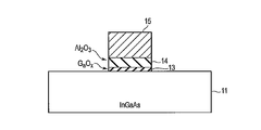
- FIG. 1 is a cross-sectional view showing a schematic structure of the field effect semiconductor device according to the first embodiment.
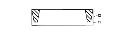
- FIG. 2A is a cross-sectional view showing the manufacturing process of the field effect semiconductor device according to the first embodiment.
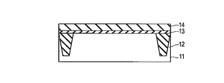
- FIG. 2B is a cross-sectional view showing the manufacturing process of the field effect semiconductor device according to the first embodiment.
- FIG. 2C is a cross-sectional view showing the manufacturing process of the field effect semiconductor device according to the first embodiment.
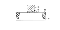
- FIG. 2D is a cross-sectional view illustrating the manufacturing process of the field effect semiconductor device according to the first embodiment.
- FIG. 2E is a cross-sectional view illustrating the manufacturing process of the field effect semiconductor device according to the first embodiment.
- FIG. 3 is a characteristic diagram showing the dependence of the film thickness of the GaO x layer on the number of times of raw material supply.
- FIG. 4 is a characteristic diagram showing the effect of interfacial layer insertion of the GaO x layer on the interface state density.
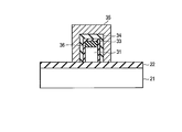
- FIG. 5A is a cross-sectional view illustrating a schematic structure of the field effect semiconductor device according to the second embodiment.
- FIG. 5B is a cross-sectional view illustrating a schematic structure of the field effect semiconductor device according to the second embodiment.
- FIG. 1 is a cross-sectional view showing a schematic structure of a field effect semiconductor device according to the first embodiment of the present invention.
- a GaO x (0 ⁇ x ⁇ 1) layer 13 having a thickness of 0.5 nm or less is formed on the semiconductor layer 11 made of In y Ga 1-y As (0 ⁇ y ⁇ 1), and Al 2 is formed thereon.
- a gate insulating film 14 made of O 3 is laminated. Further, a gate electrode 15 is formed on the gate insulating film 14. The gate electrode 15, the gate insulating film 14, and the GaO x layer 13 are processed into a gate pattern. Source / drain regions (not shown) are formed on the surface of the semiconductor layer 11 on both sides of the gate pattern.
- the film thickness of the gate insulating film 14 Although there is no restriction
- the source / drain (S / D) electrode may be formed after impurity diffusion is performed to form a diffusion layer, or as a so-called metal S / D structure in which a metal electrode such as Ni—InGaAs is adjacent to the gate end. Also good. That is, there is no restriction on the S / D structure.
- the gate insulating film 14 formed on the GaO x layer 13 is not limited to Al 2 O 3 but may be a high-k film (high dielectric constant insulating film).
- the method for forming the InGaAs layer as the semiconductor layer 11 is not limited, and it can be formed by epitaxial growth on a compound semiconductor substrate such as InP or GaAs, or a Si or Ge substrate, or by bonding to various base substrates. .
- an element isolation insulating film 12 made of an insulating film such as SiO 2 is formed on the surface portion of the semiconductor layer 11 in accordance with various substrate structures.
- a GaO x layer 13 that is a feature of the present embodiment is formed on the semiconductor layer 11.
- Trimethylgallium (TMG) or triethylgallium (TEG) can be used as the Ga raw material, and H 2 O or ozone (O 3 ) can be used as the oxidizing agent.
- the first supply source is preferably a Ga source. This is because the surface oxidation by directly supplying the oxidizing agent to the substrate surface is suppressed and the natural oxide film remaining on the substrate surface is removed by TMG or TEG. Further, it is desirable to appropriately replace the film forming chamber atmosphere with a non-source gas such as nitrogen when switching the gas.
- the film forming temperature is preferably 400 ° C. or lower, particularly 300 ° C. or lower in order to keep the interface characteristics of InGaAs as the semiconductor layer 11 good.
- FIG. 3 shows the dependence of the film thickness of GaO x formed as described above on the number of times of raw material supply (one cycle of TMG / H 2 O being supplied once).
- the film thickness was estimated by a spectroscopic ellipsometry method assuming a refractive index of Ga 2 O 3 .
- the film thickness estimated by the spectroscopic ellipsometry was obtained by analyzing the Ga2p peak in the X-ray photoelectron spectroscopy using AlK ⁇ rays as the excitation source, assuming that the escape depth of Ga2p photoelectrons is 0.8 nm. It was in good agreement with the value.
- the GaO x film formation mode differs from normal ALD ( ⁇ 0.1 nm / cycle), and almost self-stops at a film thickness of about 0.3 nm. That is, it was found that an ultrathin GaO x layer having a thickness of 0.3 nm or less can be formed accurately and uniformly without adjusting the number of times of supplying raw materials in detail.
- the fact that the growth stops at an extremely thin film thickness of 0.3 nm means that the film thickness becomes constant regardless of the number of cycles. This means that a GaO x layer with high film thickness reproducibility can be formed by a method equivalent to ALD.
- the upper limit of the film thickness was 0.3 nm.
- the film thickness did not exceed 0.5 nm even when the temperature and other conditions were changed. That is, a GaOx layer having a thickness of 0.5 nm or less can be formed by a method equivalent to ALD in which Ga source gas and oxidant gas such as water and ozone are alternately supplied.
- Al 2 O 3 is continuously formed as the gate insulating film 14 by the ALD method.
- Al 2 O 3 can be formed by changing the growth gas after forming the GaO x layer 13 in the same chamber. Therefore, the gate insulating film 14 can be easily formed, and the GaO x layer 13 can be covered with Al 2 O 3 without being exposed to the atmosphere.
- Trimethylaluminum can be used as the Al raw material for forming Al 2 O 3, and H 2 O or ozone (O 3 ) can be used as the oxidizing agent.
- the film formation temperature is 400 ° C. or less, and the film thickness is 5 nm or less. Note that heat treatment at 600 ° C. or lower may be performed after GaO x or Al 2 O 3 film formation or both.
- the GaO x / Al 2 O 3 / InGaAs MOS interface formed in this way has a minimum value of 1/2 as compared with the Al 2 O 3 / InGaAs MOS interface without the GaO x layer. It was confirmed that the interface state density was reduced. Moreover, it was confirmed that the insertion of GaO x significantly reduces the energy position dependency of the interface state density, and the difference becomes more remarkable at energy positions other than the minimum value. That is, the interface state density could be lowered over a wide energy range in the band gap.
- the so-called passivation effect that the interface state density can be reduced by inserting the GaO x layer is as follows. That is, dangling bonds existing at the interface are considered to be one of the origins of the interface state, but when GaO x is formed, an interface with few dangling bonds can be formed. . This is not necessarily limited to the interface of InGaAs, but can be expected similarly for other semiconductor materials.
- TaN for example, is deposited by sputtering as the material of the gate electrode 15 as shown in FIG. 2D. Subsequently, as shown in FIG. 2E, the gate electrode 15, the gate insulating film 14, and the GaO x layer 13 are processed into a gate pattern.
- the GaO x layer 13 having a small thickness is inserted between the semiconductor layer 11 made of In y Ga 1-y As and the gate insulating film 14 made of Al 2 O 3. Accordingly, a high-quality MOS interface can be formed, and a MOSFET having a low interface state density can be manufactured in a wide energy range in the band gap. For this reason, low power consumption is achieved by the mobility improvement and the S value reduction effect.
- the GaO x layer 13 can be manufactured by a method equivalent to ALD without using an ultrahigh vacuum deposition method. Furthermore, it is possible to form the Al 2 O 3 is a gate insulating film 14 in succession GaO x layer 13, the complexity of the process by inserting the GaO x layer 13 hardly occurs.
- FIGS. 5A and 5B are sectional views showing a schematic structure of a field effect semiconductor device according to the second embodiment of the present invention.
- FIG. 5A shows an example in which a gate electrode is formed on three surfaces of the Fin structure
- FIG. 5B shows an example in which a gate electrode is formed on two surfaces of the Fin structure.
- an In y Ga 1-y As (0 ⁇ y ⁇ 1) layer as a Fin structure (semiconductor layer) 31 is formed on the insulating film 22 on the support substrate 21.
- the Fin structure 31 may be the same material as the support substrate 21 or may be a different material.
- a gate electrode 35 is formed on the surface of the Fin structure 31 through a GaO x layer 33 and an Al 2 O 3 film 34 as a gate insulating film. That is, the GaO x layer 33 and the Al 2 O 3 film 34 are laminated on both side surfaces and the upper surface of the Fin structure 31, and the gate electrode 35 is formed thereon. The gate electrode 35 controls the channels on both side surfaces and the upper surface of the Fin structure.
- the GaO x layer 33 and the Al 2 O 3 film 34 may be formed in the same manner as in the first embodiment. Furthermore, the gate electrode 35 may be formed in the same manner as in the first embodiment.
- the insulating mask material 36 used for the Fin formation remains on the Fin structure. For this reason, the gate electrode 35 controls the channels on both side surfaces of the Fin structure.
- a high-quality MOS interface can be formed by inserting the GaO x layer 33 between the Fin structure 31 forming the channel and the gate insulating film 34, and a wide energy in the band gap can be formed.
- a MOSFET having a low interface state density in a range can be manufactured. Therefore, the same effect as the first embodiment can be obtained.
- the semiconductor layer to be a channel material is In y Ga 1-y As (0 ⁇ x ⁇ 1), but the semiconductor layer is not limited to In y Ga 1-y As. .
- the semiconductor a compound composed of some of (Al, Ga, In) (Group III element) and (N, P, As, Sb) (Group V element), for example, InP, In y Ga It can be applied to 1-y Sb (0 ⁇ y ⁇ 1) and the like.
- the channel does not need to have a uniform composition, and it is possible to adopt a structure in which the composition is changed in a graded manner or a structure in which the above compounds are arbitrarily stacked.
- the gate insulating film is not limited to Al 2 O 3 , and may be a high-k film, and HfO 2 , ZrO 2 , La 2 O 3 , or a mixture of them can be used as appropriate.
- the method for forming the GaO x layer is not necessarily limited to the same method as the ALD method in which the source gas and the oxidant gas are alternately supplied, and the GaO x layer can be grown in a range of 0.5 nm or less. If applicable.
- a GaO x layer can be grown by simultaneously supplying a Ga source gas and an oxidant gas. In this method, if the growth does not self-stop, the film thickness may be adjusted to 0.5 nm or less by adjusting the time.
- the example applied to the Fin structure has been described.
- the present invention can also be applied to nanowires.
- a gate all-around MOS can be realized.
- it is effective to apply not only to a Fin structure on an insulating film but also to a so-called bulk Fin structure manufactured on a bulk substrate.
Landscapes
- Insulated Gate Type Field-Effect Transistor (AREA)
- Thin Film Transistor (AREA)
Abstract
電界効果型半導体装置であって、半導体層(11)の表面上に形成されたGaOx 層(13)と、GaOx 層(13)の表面上に形成された、high-k 膜からなるゲート絶縁膜(14)と、ゲート絶縁膜(14)の表面上に形成されたゲート電極(15)とを備えている。そして、GaOx層13の存在により、バンドギャップ中の広いエネルギー範囲で界面準位密度を低くすることができる。
Description
本発明は、電界効果型半導体装置及びその製造方法に関する。
素子の微細化限界に直面しつつある現在、微細化によらないLSIの低消費電力化が大きな課題となっている。例えば、MOSFETのチャネルに従来のSiよりも移動度の高い III-V族半導体を用いる研究が精力的に行われている。III-V族半導体の中では、Siの5~10倍程度の電子移動度を有するInGaAsが特に有望視されている。
一方、III-V族半導体を用いた高性能MOSFETの実現には、界面準位密度の低い高品質なMOS界面の形成が必須である。そのために、原子層堆積法(ALD法)で成膜したAl2O3 (例えば、非特許文献1参照)や真空蒸着法で形成したGa2O3(Gd2O3 )(GGO)(例えば、非特許文献2参照)により、比較的良好なInGaAsのMOS界面が形成可能であることが報告されている。
R. M. Wallace et al., MRS BULLETIN, Vol. 34, p493 (2009)
M. Hong et al., MRS BULLETIN, Vol. 34, p514 (2009)
GGOを用いたMOSFETの形成では、GGOの高い吸湿性のため、GGO成膜後に、真空一環で保護酸化膜(Al2O3 等)若しくはゲート電極を形成する必要がある。この場合、成膜方式としては超高真空蒸着法を用いる必要がある。しかし、超高真空蒸着法は、量産性、大面積均一性に課題があり、工業的応用には適さない。
一方、量産性、均一性に優れるALD法を用いたAl2O3/InGaAsのMOSFETの形成では、バンドギャップ中の広いエネルギー範囲で低い界面準位密度は得られない。即ち、界面準位密度のは、バンドギャップ中での最小値では1011cm-2/eV台の値が達成されているものの、狭いエネルギー範囲で1012cm-2/eV以上に増大する。MOSFETの高性能化には、より広いエネルギー範囲でより低い界面準位密度の実現が必要である。
発明が解決しようとする課題は、バンドギャップ中の広いエネルギー範囲で界面準位密度の低いMOSFETが作製可能となり、移動度向上及びS値低減効果により低消費電力化に寄与し得る電界効果型半導体装置及びその製造方法を提供することである。
本発明の一態様に係わる電界効果型半導体装置の製造方法は、半導体層の表面上に形成されたGaOx 層と、前記GaOx 層の表面上に形成された、high-k 膜からなるゲート絶縁膜と、前記ゲート絶縁膜の表面上に形成されたゲート電極と、を具備したことを特徴とする。
また、本発明の別の一態様に係わる電界効果型半導体装置の製造方法は、半導体層の表面上にGaOx 層を形成する工程と、前記GaOx 層の表面上に、high-k からなるゲート絶縁膜を形成する工程と、前記ゲート絶縁膜の表面上にゲート電極を形成する工程と、を含むことを特徴とする。
本発明によれば、チャネルを形成するための半導体層とゲート絶縁膜との間にGaOx 層を挿入することにより、高品質のMOS界面を形成できると共に、バンドギャップ中の広いエネルギー範囲で界面準位密度の低いMOSFETが作製可能となる。従って、移動度向上、S値低減効果により、低消費電力化が達成される。
以下、本発明の詳細を図示の実施形態によって説明する。
(第1の実施形態)
図1は、本発明の第1の実施形態に係わる電界効果型半導体装置の概略構造を示す断面図である。
図1は、本発明の第1の実施形態に係わる電界効果型半導体装置の概略構造を示す断面図である。
InyGa1-yAs(0≦y≦1)からなる半導体層11上に、0.5nm以下の膜厚でGaOx(0<x<1)層13が形成され、その上にAl2O3 からなるゲート絶縁膜14が積層されている。さらに、ゲート絶縁膜14上にはゲート電極15が形成されている。ゲート電極15,ゲート絶縁膜14,及びGaOx 層13はゲートパターンに加工されている。そして、ゲートパターンの両側で半導体層11の表面部に、図示しないソース/ドレイン領域が形成されている。
ゲート絶縁膜14の膜厚に制限は無いが、実効酸化膜厚低減の観点から、5nm以下にすることが望ましい。ゲート絶縁膜14上のゲート電極材料としては、Ta,TaN,Ti,TiN,Ni,Au,Pt等の各種金属を用いることができる。また、NiSixやNiGex等の合金、更には高濃度ドーピングを施したpoly-Si1-xGex 等を用いることもできる。つまり、ゲート電極材料に制限は無い。ソース・ドレイン(S/D)電極は、不純物ドーピングを施して拡散層を形成した後に形成しても良いし、ゲート端にNi-InGaAs等の金属電極を隣接させる、いわゆるメタルS/D構造としても良い。つまり、S/D構造に制限は無い。また、GaOx 層13上に形成されるゲート絶縁膜14もAl2O3 に限るものではなく、high-k 膜(高誘電率絶縁膜)であればよい。
次に、本実施形態の電界効果型半導体装置の製造方法を、図2A~2Eを参照して説明する。
半導体層11としてのInGaAs層の形成法に制限は無く、InPやGaAs等の化合物半導体基板、若しくはSiやGe基板上にエピタキシャル成長で形成することや、各種母体基板に貼り合わせて形成することができる。
まず、図2Aに示すように、各種基板構造に応じて半導体層11の表面部に、SiO2 等の絶縁膜からなる素子分離絶縁膜12を形成する。
次いで、図2Bに示すように、半導体層11上に本実施形態の特徴であるGaOx 層13を形成する。このGaOx 成膜前には、NH4OH,(NH4)S,HF,HCl等の溶液を用いて、半導体層11上の自然酸化膜を除去することが望ましい。Ga原料としては、トリメチルガリウム(TMG)やトリエチルガリウム(TEG)を用いることができ、酸化剤としてはH2O若しくはオゾン(O3)を用いることができる。
これらの原料ガス及び酸化剤ガスを400℃以下に昇温した基板に交互に供給してGaOx の成膜を行うが、最初の供給原料はGa原料とすることが望ましい。これは、基板表面に直接酸化剤を供給することによる表面の酸化を抑制すると共に、TMGやTEGにより基板表面に残存する自然酸化膜を除去する効果があるためである。また、ガス切り替え時には、窒素等の非原料ガスによる成膜室雰囲気の置換を適宜実施することが望ましい。なお、成膜温度としては、半導体層11としてのInGaAsの界面特性を良好に保つには400℃以下、特に300℃以下が望ましい。
図3に、上記のようにして成膜されたGaOx の膜厚の、原料供給回数(TMG/H2Oそれぞれ1回供給したことをもって1サイクルとする)依存性を示す。膜厚は、Ga2O3 の屈折率を仮定し、分光エリプソメトリ法によって見積もった。なお、分光エリプソメトリ法によって見積もった膜厚は、AlKα線を励起源としたX線光電子分光法において、Ga2p光電子の脱出深さを0.8nmと仮定し、Ga2pピークの解析を行って得た値と良く一致した。GaOx の成膜様式は、通常のALD(~0.1nm/cycle)とは異なり、膜厚0.3nm程度でほぼ自己停止することが分かった。即ち、原料供給回数を詳細に調整することなく、0.3nm以下の極薄GaOx 層を精度良く均一に形成できることが分かった。
ここで、0.3nmという極めて薄い膜厚で成長が停止するのは、サイクル数によらず膜厚一定になることを意味する。これは、ALDと同等の方式で膜厚の再現性が高いGaOx 層を形成できることを意味する。
また、上記の例では膜厚の上限が0.3nmであったが、各種実験の結果、温度や他の条件を変えても、膜厚が0.5nmを越えることはなかった。即ち、Gaの原料ガスと水やオゾン等の酸化剤ガスとを交互に供給するALDと同等の方式により0.5nm以下の膜厚のGaOx層を形成することができる。
0.5nm以下のGaOx 層13の形成後、図2Cに示すように、ゲート絶縁膜14として、Al2O3 の成膜を連続してALD法によって行う。Al2O3 の形成は、同じチャンバ内でGaOx 層13を形成した後に、成長ガスを変えることによって可能である。このため、ゲート絶縁膜14の形成が容易であると共に、GaOx 層13を大気に晒すことなくAl2O3 で覆うことができる。
Al2O3 形成のためのAl原料としては、トリメチルアルミニウム(TMA)を用いることができ、酸化剤としてはH2O若しくはオゾン(O3)を用いることができる。成膜温度は、400℃以下とし、膜厚は5nm以下とする。なお、GaOx 又はAl2O3 成膜後、若しくはその両方で600℃以下の熱処理を行っても良い。
このように形成したGaOx/Al2O3/InGaAsのMOS界面では、図4に示すように、GaOx 層の無いAl2O3/InGaAsのMOS界面に比べて、最小値で1/2程度、界面準位密度が低減することが確認された。また、GaOx の挿入により界面準位密度のエネルギー位置依存性が大幅に減少し、上記最小値以外のエネルギー位置においては、その差はより顕著となることが確認された。即ち、バンドギャップ中の広いエネルギー範囲で界面準位密度を低くすることができた。
ここで、GaOx 層の挿入により界面準位密度を低減できると云う、いわゆるパッシベーション効果は、次のような理由によると推察される。即ち、界面に存在する未結合手(ダングリングボンド)が界面準位の起源の一つと考えられているが、GaOx を形成するとダングリングボンドの少ない界面を作ることが可能となるためである。これは、必ずしもInGaAsの界面に限らず、他の半導体材料でも同様に期待できる。
ゲート絶縁膜成膜後、図2Dに示すようにゲート電極15の材料として、例えばTaNをスパッタリングで堆積させる。続いて、図2Eに示すように、ゲート電極15,ゲート絶縁膜14,及びGaOx 層13をゲートパターンに加工する。
これ以降のS/D電極形成、その他の後工程に制限は無く、適宜用途に応じたプロセスを行い、InGaAsのMOSFETを作製する。また、S/D部を先に形成した後、ゲートスタックを形成する、いわゆる、ゲートラストプロセスを採用することも無論可能である。
このように本実施形態によれば、InyGa1-yAsからなる半導体層11とAl2 O3 からなるゲート絶縁膜14との間に、膜厚の薄いGaOx 層13を挿入することにより、高品質のMOS界面を形成できると共に、バンドギャップ中の広いエネルギー範囲で界面準位密度の低いMOSFETが作製可能となる。このため、移動度向上、S値低減効果により、低消費電力化が達成される。
また、GaOx 層13は、超高真空蒸着法を用いる必要なく、ALDと同等の方式で作製することが可能である。さらに、GaOx 層13に連続してゲート絶縁膜14であるAl2O3 を形成できるので、GaOx 層13を挿入することによるプロセスの複雑化は殆ど生じない。
(第2の実施形態)
図5A,5Bは、本発明の第2の実施形態に係わる電界効果型半導体装置の概略構造を示す断面図である。
図5A,5Bは、本発明の第2の実施形態に係わる電界効果型半導体装置の概略構造を示す断面図である。
本実施形態が先に説明した第1の実施形態と異なる点は、GaOx 層の挿入をFin構造に適用したことである。図5AはFin構造の3面にゲート電極を形成したもの、図5BはFin構造の2面にゲート電極を形成した例である。
図5Aに示すように、支持基板21上の絶縁膜22上にFin構造(半導体層)31としてのInyGa1-yAs(0≦y≦1)層が形成されている。このFin構造31は、支持基板21と同じ材料であっても良いし、別の材料であっても良い。
Fin構造31の表面上には、GaOx 層33及びゲート絶縁膜としてのAl2O3 膜34を介して、ゲート電極が35が形成されている。即ち、Fin構造31の両側面及び上面にGaOx 層33及びAl2O3 膜34が積層され、その上にゲート電極35が形成されている。そして、ゲート電極35はFin構造の両側面及び上面のチャネルを制御するようになっている。GaOx 層33及びAl2O3 膜34の形成は第1の実施形態と同様にすればよい。さらに、ゲート電極35の形成も第1の実施形態と同様にすればよい。
また、図5Bでは、Fin構造上にFin形成のために使用した絶縁性のマスク材36が残っている。このため、ゲート電極35はFin構造の両側面のチャネルを制御するようになっている。
このような構成であっても、チャネルを成すFin構造31とゲート絶縁膜34との間にGaOx 層33を挿入することにより、高品質のMOS界面を形成できると共に、バンドギャップ中の広いエネルギー範囲で界面準位密度の低いMOSFETが作製可能となる。従って、第1の実施形態と同様の効果が得られる。
(変形例)
なお、本発明は上述した各実施形態に限定されるものではない。
なお、本発明は上述した各実施形態に限定されるものではない。
実施形態では、チャネル材料とすべき半導体層をInyGa1-yAs(0≦x≦1)にすることを前提としていたが、半導体層はInyGa1-yAsに限るものではない。本発明では、半導体としては、(Al,Ga,In)(III族元素)と(N,P,As,Sb)(V族元素)の幾つかで構成される化合物、例えばInP,InyGa1-ySb(0≦y≦1)等に適用することができる。さらに、(C,Si,Ge,Sn)(IV族元素)の幾つかで構成される化合物、例えばSiyGe1-y(0≦y≦1)に適用することも可能である。また、無論、チャネルは均一組成である必要はなく、傾斜的に組成が変調されたものや上記化合物が任意に積層された構造にも採用することが可能である。
また、ゲート絶縁膜はAl2O3 に限るものではなく、high-k 膜であればよく、HfO2 ,ZrO2 ,La2O3 、又はこれらを適宜混合したものを用いることができる。
また、GaOx 層の形成方法は、必ずしも原料ガスと酸化剤ガスを交互に供給するALD法と同等の方式に限るものではなく、GaOx 層を0.5nm以下の範囲で成長できる方法であれば適用可能である。例えば、Ga原料ガスと酸化剤ガスを同時に供給してGaOx 層を成長することも可能である。この方法で、もし成長が自己停止しない場合は、時間調整で膜厚を0.5nm以下にすればよい。
また、第2の実施形態ではFin構造に適用した例を説明したが、本発明はナノワイヤーに適用することも可能である。この場合、ゲートオールアラウンドのMOSを実現することが可能となる。また、絶縁膜上のFin構造のみならず、バルク基板上に作製した、いわゆるバルクFin構造に適用することも無論有効である。
本発明の幾つかの実施形態を説明したが、これらの実施形態は、例として提示したものであり、発明の範囲を限定することは意図していない。これら実施形態は、その他の様々な形態で実施されることが可能であり、発明の要旨を逸脱しない範囲で、種々の省略、置き換え、変更を行うことができる。これら実施形態やその変形は、発明の範囲や要旨に含まれると同様に、特許請求の範囲に記載された発明とその均等の範囲に含まれるものである。
11…InyGa1-yAs層(半導体層)
12…素子分離絶縁膜
13,33…GaOx 層
14,34…Al2O3 膜(ゲート絶縁膜)
15,35…ゲート電極
21…支持基板
22…絶縁膜
31…InyGa1-yAs層(Fin構造)
36…マスク材
12…素子分離絶縁膜
13,33…GaOx 層
14,34…Al2O3 膜(ゲート絶縁膜)
15,35…ゲート電極
21…支持基板
22…絶縁膜
31…InyGa1-yAs層(Fin構造)
36…マスク材
Claims (18)
- 半導体層の表面上に形成されたGaOx 層と、
前記GaOx 層の表面上に形成された、high-k 膜からなるゲート絶縁膜と、
前記ゲート絶縁膜の表面上に形成されたゲート電極と、
を具備したことを特徴とする電界効果型半導体装置。 - 前記半導体層は、InyGa1-yAs(0≦y≦1),InP,InyGa1-ySb(0≦y≦1),SiyGe1-y(0≦y≦1)の何れかであることを特徴とする請求項1記載の電界効果型半導体装置。
- 前記GaOx 層は、膜厚が0.5nm以下であることを特徴とする請求項1記載の電界効果型半導体装置。
- 前記GaOx 層は、膜厚が0.3nm以下であることを特徴とする請求項1記載の電界効果型半導体装置。
- 前記ゲート絶縁膜は、Al2O3 で形成されていることを特徴とする請求項1記載の電界効果型半導体装置。
- 支持基板上にフィン状に形成された半導体層と、
前記半導体層の表面上に形成されたGaOx 層と、
前記GaOx 層の表面上に形成された、high-k 膜からなるゲート絶縁膜と、
前記ゲート絶縁膜の表面上に形成されたゲート電極と、
を具備したことを特徴とする電界効果型半導体装置。 - 前記半導体層は、InyGa1-yAs(0≦y≦1),InP,InyGa1-ySb(0≦y≦1),SiyGe1-y(0≦y≦1)の何れかであることを特徴とする請求項5記載の電界効果型半導体装置。
- 前記GaOx 層は、膜厚が0.5nm以下であることを特徴とする請求項6記載の電界効果型半導体装置。
- 前記GaOx 層は、膜厚が0.3nm以下であることを特徴とする請求項6記載の電界効果型半導体装置。
- 前記ゲート絶縁膜は、Al2O3 で形成されていることを特徴とする請求項6記載の電界効果型半導体装置。
- 半導体層の表面上にGaOx 層を形成する工程と、
前記GaOx 層の表面上に、high-k からなるゲート絶縁膜を形成する工程と、
前記ゲート絶縁膜の表面上にゲート電極を形成する工程と、
を含むことを特徴とする電界効果型半導体装置の製造方法。 - 前記GaOx 層を形成する工程として、前記半導体層の表面部にGaの原料ガスと酸化剤ガスとを交互に供給して前記GaOx 層を成長することを特徴とする請求項11記載の電界効果型半導体装置の製造方法。
- 前記GaOx 層を成長する際の成膜温度を400℃以下に設定したことを特徴とする請求項12記載の電界効果型半導体装置の製造方法。
- 前記原料ガスと前記酸化剤ガスとを交互に供給する際に、最初に前記原料ガスの供給を行うことを特徴とする請求項12記載の電界効果型半導体装置の製造方法。
- 前記GaOx 層と前記ゲート絶縁膜を、同一チャンバ内で連続して形成することを特徴とする請求項11記載の電界効果型半導体装置の製造方法。
- 前記GaOx 層の形成前に、前記半導体層の表面の自然酸化膜を除去するために、溶液を用いて表面処理することを特徴とする請求項11記載の電界効果型半導体装置の製造方法。
- 前記GaOx 層の成長膜厚を0.5nm以下に設定することを特徴とする請求項12記載の電界効果型半導体装置の製造方法。
- ゲート絶縁膜として、Al2 O3 を用いることを特徴とする請求項11記載の電界効果型半導体装置の製造方法。
Applications Claiming Priority (2)
| Application Number | Priority Date | Filing Date | Title |
|---|---|---|---|
| JP2012241762A JP2014093348A (ja) | 2012-11-01 | 2012-11-01 | 電界効果型半導体装置及びその製造方法 |
| JP2012-241762 | 2012-11-01 |
Publications (1)
| Publication Number | Publication Date |
|---|---|
| WO2014069032A1 true WO2014069032A1 (ja) | 2014-05-08 |
Family
ID=50626963
Family Applications (1)
| Application Number | Title | Priority Date | Filing Date |
|---|---|---|---|
| PCT/JP2013/066369 Ceased WO2014069032A1 (ja) | 2012-11-01 | 2013-06-13 | 電界効果型半導体装置及びその製造方法 |
Country Status (3)
| Country | Link |
|---|---|
| JP (1) | JP2014093348A (ja) |
| TW (1) | TW201419535A (ja) |
| WO (1) | WO2014069032A1 (ja) |
Families Citing this family (1)
| Publication number | Priority date | Publication date | Assignee | Title |
|---|---|---|---|---|
| JP7130986B2 (ja) * | 2018-03-01 | 2022-09-06 | 富士電機株式会社 | 半導体装置の製造方法 |
Citations (6)
| Publication number | Priority date | Publication date | Assignee | Title |
|---|---|---|---|---|
| JP2005328059A (ja) * | 2004-05-14 | 2005-11-24 | Internatl Business Mach Corp <Ibm> | 高誘電率ゲート酸化物を有する電界効果トランジスタの閾値及びフラットバンド電圧安定化層 |
| JP2008521215A (ja) * | 2004-11-15 | 2008-06-19 | インターナショナル・ビジネス・マシーンズ・コーポレーション | 半導体構造およびそれを形成する方法(金属酸化物の付着を介して形成されたしきい電圧制御層を含む窒素含有電界効果トランジスタ・ゲート・スタック) |
| JP2010093247A (ja) * | 2008-09-16 | 2010-04-22 | Imec | 非シリコンチャネルmosデバイス中のフェルミレベルピンニングの低減方法 |
| JP2010153845A (ja) * | 2008-11-28 | 2010-07-08 | Sumitomo Chemical Co Ltd | 半導体基板の製造方法、半導体基板、電子デバイスの製造方法、および反応装置 |
| JP2010272632A (ja) * | 2009-05-20 | 2010-12-02 | Furukawa Electric Co Ltd:The | 電界効果トランジスタ |
| JP2011192834A (ja) * | 2010-03-15 | 2011-09-29 | Advanced Power Device Research Association | 半導体装置および半導体装置の製造方法 |
-
2012
- 2012-11-01 JP JP2012241762A patent/JP2014093348A/ja active Pending
-
2013
- 2013-06-13 WO PCT/JP2013/066369 patent/WO2014069032A1/ja not_active Ceased
- 2013-06-20 TW TW102121930A patent/TW201419535A/zh unknown
Patent Citations (6)
| Publication number | Priority date | Publication date | Assignee | Title |
|---|---|---|---|---|
| JP2005328059A (ja) * | 2004-05-14 | 2005-11-24 | Internatl Business Mach Corp <Ibm> | 高誘電率ゲート酸化物を有する電界効果トランジスタの閾値及びフラットバンド電圧安定化層 |
| JP2008521215A (ja) * | 2004-11-15 | 2008-06-19 | インターナショナル・ビジネス・マシーンズ・コーポレーション | 半導体構造およびそれを形成する方法(金属酸化物の付着を介して形成されたしきい電圧制御層を含む窒素含有電界効果トランジスタ・ゲート・スタック) |
| JP2010093247A (ja) * | 2008-09-16 | 2010-04-22 | Imec | 非シリコンチャネルmosデバイス中のフェルミレベルピンニングの低減方法 |
| JP2010153845A (ja) * | 2008-11-28 | 2010-07-08 | Sumitomo Chemical Co Ltd | 半導体基板の製造方法、半導体基板、電子デバイスの製造方法、および反応装置 |
| JP2010272632A (ja) * | 2009-05-20 | 2010-12-02 | Furukawa Electric Co Ltd:The | 電界効果トランジスタ |
| JP2011192834A (ja) * | 2010-03-15 | 2011-09-29 | Advanced Power Device Research Association | 半導体装置および半導体装置の製造方法 |
Also Published As
| Publication number | Publication date |
|---|---|
| JP2014093348A (ja) | 2014-05-19 |
| TW201419535A (zh) | 2014-05-16 |
Similar Documents
| Publication | Publication Date | Title |
|---|---|---|
| US8124513B2 (en) | Germanium field effect transistors and fabrication thereof | |
| TWI397124B (zh) | 半導體裝置的製造方法 | |
| US10847424B2 (en) | Method for forming a nanowire device | |
| CN102339858B (zh) | p型半导体器件及其制造方法 | |
| CN111384178B (zh) | 半导体器件以及用于制造此类半导体器件的方法 | |
| US9245970B2 (en) | Semiconductor structure having interfacial layer and high-k dielectric layer | |
| CN106486549A (zh) | 用于finfet器件中的栅极氧化物的均匀性的平坦sti表面 | |
| TW201409697A (zh) | 具有鎢閘極電極的半導體裝置及其製造方法 | |
| JP2016018888A (ja) | 半導体装置およびその製造方法 | |
| KR101521555B1 (ko) | 게르마늄 응축 공정을 이용한 기판 제조 방법 및 이를 이용한 반도체 소자의 제조 방법 | |
| US9954077B2 (en) | Apparatus and method for multiple gate transistors | |
| Litta et al. | Thulium silicate interfacial layer for scalable high-k/metal gate stacks | |
| US8404575B2 (en) | Semiconductor device and method for manufacturing same | |
| KR20070112783A (ko) | 질화 게이트 유전체의 제조 방법 | |
| US8232581B2 (en) | Method for manufacturing an III-V engineered substrate and the III-V engineered substrate thereof | |
| WO2004107451A1 (ja) | Mis型電界効果トランジスタを備える半導体装置及びその製造方法並びに金属酸化膜の形成方法 | |
| CN106571387A (zh) | 基于高K材料的叠栅AlGaN/GaN高电子迁移率MOS器件 | |
| TW201830526A (zh) | 製造半導體裝置的方法 | |
| TWI546958B (zh) | Gold and oxygen semi - high electron mobility transistor | |
| JP2014093348A (ja) | 電界効果型半導体装置及びその製造方法 | |
| KR20150014321A (ko) | 반도체 소자 및 그 제조 방법 | |
| JP2013008832A (ja) | 化合物半導体装置の製造方法 | |
| CN106876460B (zh) | 具有不对称结构的晶体管的形成方法 | |
| CN102054680A (zh) | 一种克服钼基金属栅叠层结构制备中钼与硅反应的方法 | |
| TWI653688B (zh) | 半導體裝置及其製造方法 |
Legal Events
| Date | Code | Title | Description |
|---|---|---|---|
| 121 | Ep: the epo has been informed by wipo that ep was designated in this application |
Ref document number: 13851616 Country of ref document: EP Kind code of ref document: A1 |
|
| NENP | Non-entry into the national phase |
Ref country code: DE |
|
| 122 | Ep: pct application non-entry in european phase |
Ref document number: 13851616 Country of ref document: EP Kind code of ref document: A1 |