WO2014065372A1 - 砥粒付ワイヤ工具 - Google Patents
砥粒付ワイヤ工具 Download PDFInfo
- Publication number
- WO2014065372A1 WO2014065372A1 PCT/JP2013/078834 JP2013078834W WO2014065372A1 WO 2014065372 A1 WO2014065372 A1 WO 2014065372A1 JP 2013078834 W JP2013078834 W JP 2013078834W WO 2014065372 A1 WO2014065372 A1 WO 2014065372A1
- Authority
- WO
- WIPO (PCT)
- Prior art keywords
- wire
- abrasive grains
- plating
- abrasive
- holes
- Prior art date
- Legal status (The legal status is an assumption and is not a legal conclusion. Google has not performed a legal analysis and makes no representation as to the accuracy of the status listed.)
- Ceased
Links
Images


Classifications
-
- B—PERFORMING OPERATIONS; TRANSPORTING
- B24—GRINDING; POLISHING
- B24B—MACHINES, DEVICES, OR PROCESSES FOR GRINDING OR POLISHING; DRESSING OR CONDITIONING OF ABRADING SURFACES; FEEDING OF GRINDING, POLISHING, OR LAPPING AGENTS
- B24B27/00—Other grinding machines or devices
- B24B27/06—Grinders for cutting-off
- B24B27/0633—Grinders for cutting-off using a cutting wire
-
- B—PERFORMING OPERATIONS; TRANSPORTING
- B28—WORKING CEMENT, CLAY, OR STONE
- B28D—WORKING STONE OR STONE-LIKE MATERIALS
- B28D5/00—Fine working of gems, jewels, crystals, e.g. of semiconductor material; apparatus or devices therefor
- B28D5/04—Fine working of gems, jewels, crystals, e.g. of semiconductor material; apparatus or devices therefor by tools other than rotary type, e.g. reciprocating tools
- B28D5/045—Fine working of gems, jewels, crystals, e.g. of semiconductor material; apparatus or devices therefor by tools other than rotary type, e.g. reciprocating tools by cutting with wires or closed-loop blades
Definitions
- the present invention relates to a wire tool with abrasive grains, and more particularly to a wire tool with abrasive grains in which abrasive grains are fixed to the outer peripheral surface of a wire by plating.
- wafers for solar power generation, for semiconductor devices, for LED devices or for growth substrates thereof are cut (including slices) using a dedicated cutting machine such as a multi-wire saw capable of obtaining a large number of wafers at one time.
- a dedicated cutting machine such as a multi-wire saw capable of obtaining a large number of wafers at one time.
- a wire tool with abrasive grains in which abrasive grains such as diamond particles are fixed to the outer peripheral surface is increasingly used.
- the following methods are known as methods for fixing abrasive grains (diamond particles etc.), and there are advantages and disadvantages as follows.
- (A) The method of fixing the abrasive grains with a resin is prepared by applying a mixture of resin and abrasive grains to a wire.
- the method of fixing by plating prepares a plating solution in which the abrasive grains are suspended, immerses the wire in the plating solution, and deposits the plating on the outer peripheral surface of the wire and coeposits the abrasive grains. It is for this reason, since the production efficiency at the time of producing an abrasive grain equipped wire tool is low, manufacturing cost is high. Moreover, it is said that the processing damage of the cut surface of a work material (wafer etc.) is large.
- the abrasive grains are fixedly adhered to the outer peripheral surface of the wire, and the adhered abrasive grains are randomly (irregularly) distributed on the outer peripheral surface of the wire.
- unnecessary abrasive grains that do not contribute to or inhibit cutting are also fixed. For this reason, the cost of the abrasive grain attached wire tool becomes high, and deterioration of cutting quality (roughness of the cut surface, shape change, etc.) of the material to be cut (wafer, etc.) is caused, and dispersion of quality is caused, and high efficiency processing Was inhibiting.
- chips (chips) generated by the predetermined fixed abrasives may be sandwiched between the fixed abrasives, or a work material may be cut by the adjacent fixed abrasives ( The wafer may be pressed against the wafer (or the like), leading to a reduction in cutting efficiency and deterioration in cutting quality (roughness of the cut surface, shape change, etc.).
- C At the time of cutting, since the fixed particles are continuously fixed in a helical curve, the wire is twisted, and there is a possibility that the wire may be broken due to twisting.
- the present invention solves the problems as described above, facilitates the discharge of chips and coolant, enables highly efficient cutting, and obtains a wire tool with abrasive grains for producing a high-quality wafer. It is in.
- a wire tool with abrasive grains according to the present invention comprises a wire, and abrasive grains fixed by current hole plating to current holes provided at a plurality of locations of an insulating layer covering the outer peripheral surface of the wire. And the current-carrying holes are arranged on the same line with a gap therebetween.
- the insulating layer is removed.
- the surface of the abrasive grains, the surface of the conductive hole plating, and the outer peripheral surface of the wire excluding the surface of the abrasive grains and the surface of the conductive hole plating are all surface plated It is characterized by being covered.
- the entire surface plating is a composite plating in which one or more of fine abrasive grains, cerium oxide fine particles and fine zircon sand are mixed.
- the gap is also the same in any pair of the current-carrying holes adjacent to each other.
- the conduction holes are circular, and a gap between the conduction holes is larger than 1/3 of a radius of the circle.
- the current-carrying holes are disposed on one or a plurality of spiral curves on the outer peripheral surface of the wire.
- the conduction holes are equiangularly arranged in a circumferential direction of the wire on a straight line parallel to the longitudinal direction of the wire. It features.
- one abrasive grain or a plurality of aggregated abrasive grains are fixed to each of the current-carrying holes, and the diameter of the one abrasive grain is fixed. Alternatively, the diameter of the mass is equal to or less than the diameter of the current-carrying hole.
- the outer peripheral surface of the abrasive is previously treated to be a material capable of conducting the surface of the abrasive before being fixed to the current-carrying hole. It is characterized by
- the abrasive grain equipped wire tool according to the present invention has the following effects since it has the above-mentioned configuration.
- (I) The conduction holes are disposed on the same line with a gap therebetween. For this reason, since the abrasive grains fixed to the current supply holes are separated from each other, a chip (chip) or coolant (cutting fluid) generated by a predetermined abrasive grain is between the adjacent abrasive grains Since it does not get caught, it slips between the predetermined abrasive grains and the abrasive grains adjacent to the abrasive grains and flows out, so clogging is suppressed and the effect of the coolant (cooling effect etc.) is enhanced and the cutting edge height is maintained.
- the chip and the coolant can pass by the abrasive grains, and for example, the discharge direction of the chip and the coolant in which a plurality of abrasive grains are gathered is guided in a certain direction Since the discharge direction of the tip and the coolant is not defined in a fixed direction (it is random), the possibility of wire breakage due to wire twisting can be reduced.
- abrasive grains are fixed to the current-carrying holes of the determined area (volume), a large amount of abrasive grains are not fixed unnecessarily, so the amount of raw material (abrasive grains) used can be reduced. The manufacturing cost can be reduced.
- a cutting edge is formed such that the amount of protrusion of the abrasive grains is increased, and therefore, the sharpness that can withstand cutting can be maintained.
- Vi Since the underlying plating covering the surface of the abrasive grains, the surface of the current hole plating and the outer peripheral surface of the wire is covered by the entire surface plating, the fixation of the abrasive grains is further strengthened and the wear of the outer peripheral surface of the wire Is further reduced. Thus, the further extension of the tool life reduces the working cost of cutting.
- the entire surface plating is a combination plating of one or more of fine abrasive grains, fine particles of cerium oxide and fine zircon sand, thereby cooperating with the abrasive grains to resist It also has the effect of improving wear resistance and adhesion resistance or lapping properties of chips, and the fine abrasive grains and the like being plated and co-deposited contribute to the cutting of wafers etc., thus improving cutting efficiency and cutting quality. (The reduction of rough surface and shape change of the cut surface) is further promoted.
- the gap between the current-carrying holes in the circumferential direction and the gap in the longitudinal direction may be the same or different. (When deployed in a plane, they may be arranged in a grid or may not be arranged in a grid).
- the current-carrying holes are arranged on a large number of spiral curves, the current-carrying holes are uniformly arranged on one spiral curve, and the other holes are uniformly arranged on the other spiral curve opposite to the spiral curve.
- the gap between the current-carrying holes may not necessarily be the same as the gap between the current-carrying holes disposed on one spiral curve or the gap between the current-carrying holes disposed on the other spiral curve.
- the current-carrying holes are arranged in one or more spiral curves, arranged on a straight line parallel to the longitudinal direction of the wire, or on a circumference perpendicular to the longitudinal direction of the wire The arrangement of the holes facilitates the formation of the conduction holes.
- the gap between the current-carrying holes in the circumferential direction and the gap in the longitudinal direction may be the same or different. You may
- the diameter of the wire can be reduced, the cutting allowance can be reduced, and the material yield of the work material (for example, a material such as a wafer) at the time of cutting can be improved. Manufacturing costs can be reduced.
- the material yield of the work material for example, a material such as a wafer
- Manufacturing costs can be reduced.
- by using a collection of a large number of fine abrasive grains (clusters) it is possible to reduce processing damage at the time of cutting (roughness and modification of the cut surface), so the product after cutting The surface quality of (for example, a wafer) can be improved.
- the diameter of one abrasive grain or the diameter of a lump is equal to or less than the diameter of the current passing hole, a gap is formed between one abrasive grain or the lumps, so the effect (i) Etc. are obtained.
- the outer peripheral surface of the abrasive is treated so as to be a material capable of electrically conducting the surface of the abrasive before being fixed to the electrically conducting hole, the material and the electrically conducting hole capable of electrically conducting the surface of the abrasive The bond with the plating is tighter and the fixation of the abrasive is tighter. In addition, even if it uses the abrasive grain which is not processed, such an abrasive grain can be fixed.
- FIG. 2 is a cross-sectional view in a front view and a cross-sectional view showing an enlarged cross section in a front view of the abrasive grain attached wire tool shown in FIG. 1;
- positioning of the electricity supply hole of the wire tool with an abrasive grain shown in FIG. 1 (uniformly arranged on the straight line parallel to an axial direction).
- FIG. 8 is an explanatory cross-sectional view showing an abrasive grain equipped wire tool according to a second embodiment of the present invention, in which a cross section in a front view is enlarged;
- FIG. 10 is an explanatory cross-sectional view showing an abrasive grain equipped wire tool according to a third embodiment of the present invention, in which a cross section in a front view is enlarged;
- FIG. 10 is an explanatory cross-sectional view showing a wire tool with abrasive grains according to a fourth embodiment of the present invention, in which a cross section in a front view is enlarged.
- FIG. 16 is an explanatory cross-sectional view showing an abrasive grain equipped wire tool according to a fifth embodiment of the present invention, in which a cross section in a front view is enlarged;
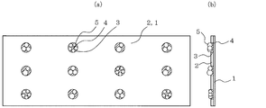
- FIGS. 1 and 2 illustrate a wire tool with abrasive grains according to a first embodiment of the present invention, wherein (a) of FIG. 1 is a side view and (b) of FIG. FIG. 2A is a cross-sectional view in a front view, and FIG. 2B is a cross-sectional view showing an enlarged cross section in a front view.
- the respective drawings are schematically illustrated, and Embodiment 1 is not limited to the illustrated embodiment, and in particular, the relative size (thickness) is exaggerated.
- a wire tool with abrasive grains (hereinafter referred to as "wire tool") 100 removes wire 1, insulating layer 2 covering the outer peripheral surface of wire 1, and part of insulating layer 2 A conductive hole 3 for exposing the outer peripheral surface of the wire 1 and an abrasive grain 5 fixed to the conductive hole 3 by the conductive hole plating 4 are provided. As described later, after fixing the abrasive grains 5, the insulating layer 2 may be removed, or after the insulating layer 2 is removed, the whole may be covered by "overall plating".
- the wire 1 is a wire having conductivity, and enables plating eutectic deposition and has a strength enough to withstand a tensile force acting on the wire 1 when cutting a wafer or the like.
- the outer diameter (D) of the wire 1 is determined by the cutting machine used, the tensile force acting on the wire, the wafer thickness, the number of wafers, and the environment and conditions of the cutting operation. Further, as described later, the size and arrangement of the current-carrying holes 3 or the size of the abrasive grains 5 may be appropriately selected according to the environment, conditions, and the like of the cutting operation.
- the material of the wire 1 is not limited, and is a high carbon piano wire, a stainless steel wire having high strength or high corrosion resistance, a maraging steel wire, or the like.
- the insulating layer 2 is for forming the conduction holes 3 and prevents the plating solution (the abrasive grains 5 for plating eutectoid mixing) from coming into contact with positions other than the conduction holes 3. There is. Therefore, the material (synthetic resin etc.) which forms the insulating layer 2 is not limited, and partial removal is easy for formation of the electricity supply hole 3, and it is for plating eutectoid (electroconductive hole plating 4 is formed Is desirable not to peel off.
- the thickness of the insulating layer 2 is selected depending on the size of the abrasive grains 5.
- the insulating layer 2 may be removed after the abrasive grains 5 are fixed. By removing it, a cutting edge is formed such that the amount of protrusion of the abrasive grains 5 is increased, and therefore, it is possible to maintain the sharpness that can withstand cutting.
- the conduction hole 3 is a part where the insulating layer 2 is partially removed and the outer peripheral surface of the wire 1 is exposed.
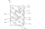
- the conduction holes 3 are cylindrical with a predetermined diameter, and are arranged at uniform intervals on one spiral curve 30 (drawn as a straight line in the developed view) on the outer peripheral surface of the wire 1.
- a gap G (exactly, a gap in the longitudinal direction) between the closest conductive holes 3 is larger than 1/3 of the radius R of the conductive holes 3 (G> R / 3).
- the formation procedure of the electrically-conductive hole 3 is not limited, either, For example, a laser beam etc. may be used to thermally remove a part thermally, or a part may be removed mechanically mechanically.
- the reason why the conduction hole 3 is made cylindrical is that the formation of the conduction hole 3 is easy, and the present invention does not limit the shape of the conduction hole 3 to a cylindrical shape. If the shape of the conduction hole 3 is not cylindrical, an equivalent cylinder of approximately the same volume (or cross-sectional area) is determined, and the gap between the conduction holes 3 closest to each other is larger than 1/3 of the radius R of the equivalent cylinder. Let's do it.
- the conduction hole 3 on the spiral curve 30 in the first turn and the conduction hole 3 on the spiral curve 30 in the second turn are close to each other.
- the clearance (H) between the closest ones of the above is larger than 1/3 of the radius R of the current-carrying hole 3 (H> R / 3).
- the conduction holes 3 are not limited to those arranged in a single spiral curve, and may be equally arranged in a large number of spiral curves, or equally divided in the circumferential direction of the wire 1 It may be evenly arranged on a line parallel to the axial direction at a plurality of arranged positions (this will be described in detail later).
- Electrode plating The conductive hole plating 4 is formed in the conductive hole 3 when the plating solution in which the abrasive grains 5 are mixed is subjected to plating coprecipitation (in the case of electrodeposition plating, when the abrasive grains 5 mixed in the plating solution are deposited).
- the abrasive grains 5 are firmly fixed to the surface of the wire 1.
- the procedure of electrodeposition plating is not limited, the use of nickel (Ni) plating or nickel-phosphorus (Ni-P) alloy plating results in high plating hardness and therefore wear resistance. And the holding power of the abrasive grains 5 can be increased.
- the abrasive 5 is, for example, hard particles such as silicon carbide, aluminum oxide, boron carbide, diamond, silicon nitride and the like. That is, they are the third, fourth or fifth group of the periodic table such as boron, silicon, aluminum, titanium, vanadium and the carbides, nitrides or oxides thereof.
- one abrasive grain 5 is fixed for each current passing hole 3 (at this time, the outer diameter of the abrasive grain 5 is smaller than the inner diameter of the current passing hole 3), but one will be described later.
- the plurality of abrasive grains 5 may be fixed to the current-carrying holes 3 of the above.
- the wire tool 100 Since the conductive holes 3 are arranged on the same line with a gap therebetween, the abrasive grains 5 fixed to the conductive holes 3 are also separated by a gap, and therefore generated by the predetermined abrasive grains 5
- a chip (chip, not shown) is not sandwiched between adjacent abrasive grains 5 and a material to be cut (wafer etc., illustrated by abrasive grains 5 with chips generated by predetermined abrasive grains 5 adjacent to each other) No risk of being pressed by Moreover, since the discharge
- the abrasive grains 5 are fixed to the conduction holes 3 of the determined area and the abrasive grains 5 are not fixed to the positions other than the conduction holes 3, a large amount of abrasive grains are not fixed unnecessarily. The amount of (abrasive grains) used can be reduced, and the manufacturing cost can be reduced. Further, since the conduction holes 3 are circular, the formation of the conduction holes 3 is easy, and the gap (G) between the conduction holes 3 is larger than 1/3 of the radius R of the conduction holes (G> R / From 3), the discharge of the tip and the coolant is promoted. Furthermore, even if the abrasive grains 5 fall off from the outer peripheral surface of the wire 1, they do not aggregate on the neighboring abrasive grains 5. Therefore, the cutting amount is stabilized and the cutting load is stabilized.
- the current flow holes are uniformly arranged in a single spiral curve, the formation of the current flow holes 3 is facilitated. If the gap (G) between the conduction holes 3 is increased, discharge of the chip and the coolant is promoted, but if the gap (G) and the pitch (P) are increased, per unit area of the outer peripheral surface of the wire 1 The number of abrasive grains (or agglomerates of abrasive grains) is reduced (the rate of abrasive grains is reduced). For this reason, the gap (G) and the pitch (P) are determined from the use conditions of the wire tool 100. For example, the gap (G) is approximately 30 times or less the radius R of the conduction hole Is desirable.
- FIG. 3 and FIG. 4 are developed views developed in a plane to explain variations of the arrangement of the conduction holes, and FIG. 3 is evenly arranged on a large number of spiral curves, and FIG. It is equally arranged on a straight line parallel to the axial direction at a plurality of positions equally divided in the circumferential direction.
- the same or corresponding parts as in FIG. 1 are denoted by the same reference numerals, and part of the description will be omitted.
- each drawing is schematically drawn and is not limited to the illustrated embodiment, and in particular, the relative size (thickness) is exaggerated.
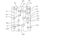
- the current-carrying holes 3 are disposed on the first spiral curve 30 a and the second spiral curve 30 b of the same pitch on the outer peripheral surface of the wire 1 with the same clearance. That is, in the first spiral curve 30a, the current-flowing holes 3a of the radius Ra are arranged at a constant value such that the gap (more precisely, the gap in the longitudinal direction) Ga is larger than 1/3 of the radius Ra.
- the conduction holes 3b of radius Rb are arranged on the curve 30b at a constant value such that the gap between them (more precisely, the clearance in the longitudinal direction) Gb is larger than 1/3 of the radius Rb. It is a generic term for the holes 3a and the current-carrying holes 3b).
- the description of suffixes “a, b” may be omitted for the common contents.
- the gap Hab between the closest ones of the conduction hole 3a on the first spiral curve 30a and the conduction hole 3b on the second spiral curve 30b is larger than 1/3 of the radius Ra and the radius Rb. (Hab> Ra / 3, and Hab> Rb / 3).
- the present invention is not limited to this, and may be three or more.
- the radius Ra and the radius Rb may be equalized, and the gap Ga and the gap Gb may be equalized.
- the conduction holes 3 are equiangularly arranged (at intervals of 90 °) at four places in the circumferential direction of the outer peripheral surface of the wire 1 and on straight lines 30 c, 30 d, 30 e, 30 f parallel to the axial direction of the wire 1. In each case, the gaps are the same. In the following description, the description of suffixes “c, d, e, f” of reference numerals may be omitted for common contents. That is, the conduction holes 3c of radius Rc are arranged on the straight line 30c, and the mutual gaps Gc are arranged at a constant value larger than 1/3 of the radius Rc.
- the straight lines 30d, 30e, and 30f respectively have radius Rd
- the conduction holes 3d, 3e and 3fc of Re and Rf are arranged at constant values in which the gaps Gd, Ge and Gf are larger than 1/3 of the radii Rd, Re and Rf.
- the clearance Hcd between the closest ones of the conduction holes 3c on the straight line 30c and the conduction holes 3d on the straight line 30d is larger than 1/3 of the radius Rc and the radius Rd (Hcd> Rc / 3, and Hcd> Rd / 3).
- the clearance Hde between the closest ones of the conduction holes 3d on the straight line 30d and the conduction holes 3e on the straight line 30e is larger than 1/3 of the radius Rd and the radius Re (Hde> Rd / 3 and Hde> Re / 3).
- “Hef> Re / 3 and Hef> Rf / 3” and “Hfc> Rf / 3 and Hfc> Rc / 3” are obtained.
- the present invention is not limited to this and may be five or more. Further, the respective radii Rc, Rd,... May be equalized (in this case, the gaps Gc, Gd,... Between the respective ones become equal). At this time, even if the conduction holes 3 disposed on a straight line can be regarded as disposed on a spiral curve as shown in FIG. 3 (Similarly, the conduction holes 3 disposed on a spiral curve) Even in some cases, it can be regarded as being placed on a straight line). Furthermore, the current-carrying holes 3c, 3d, 3e, 3f may be arranged in a grid.
- FIGS. 5 to 8 illustrate variations of the fixed state of the abrasive grains, wherein (a) is a developed view developed in a plane, and (b) is a cross-sectional view showing a cross section of a portion developed in a plane is there.
- the same or corresponding parts as in FIG. 1 are denoted by the same reference numerals, and part of the description will be omitted.
- spherical abrasive grains are illustrated, the present invention does not limit the shape of the abrasive grains to spherical.
- the conducting holes 3 shown in FIG. 5 to FIG. 8 are arranged at the same position in the axial direction, so in FIG.
- the radiuses Rc, Rd,... are equal to each other (precisely, the conductive holes 3 and the like are arranged at the same position in the axial direction at any position).
- the variation of the fixing situation of the abrasive grains can be applied to the embodiments shown in the second to fifth embodiments (FIGS. 9 to 12) described separately. is there.
- one abrasive particle 5 is fixed to each of the current supply holes 3.
- the diameter of the abrasive grains 5 is smaller than the diameter of the current passing hole 3 (for example, 40 to 60% of the diameter of the current passing hole 3). That is, the diameter of the abrasive grains mixed in the plating solution is made smaller than the diameter of the current passing hole 3.
- the center of the abrasive grains 5 and the center of the current-flowing holes 3 do not usually coincide with each other, and the amount of deviation and the direction of deviation are random.
- abrasive grain 5 In FIG. 6, several (about 2 to 5) abrasive grains 5 are fixed to each of the current-flowing holes 3 and the abrasive grains 5 are also joined by contact or plating. At this time, the diameter of the abrasive grains 5 is smaller than about 1 ⁇ 2 of the current-carrying holes 3 and larger than about 1/12. That is, since the diameter of the abrasive grains to be mixed in the plating solution is in the above range, the number of abrasive grains 5 to be fixed and the bonding form are different for each of the current-carrying holes 3.
- a large number (approximately 10 or more) of fine (for example, 1/12 or less of the diameter of the conduction hole 3) abrasive grains 5 are arranged in substantially the same plane in each of the conduction holes 3.
- the abrasive grains 5 are also bonded by plating. That is, the surfaces (apexes) of the abrasive grains 5 fixed to the current passing holes 3 are located substantially in the same plane. Then, since fine abrasive grains are mixed in the plating solution and subjected to plating co-precipitation, the number of the abrasive grains 5 to be fixed and the bonding form are different for each of the current-carrying holes 3.
- FIG. 8 shows that the fine abrasive grains 5 are accumulated and fixed in a three-dimensional manner in the conduction hole 3. That is, even when the diameter of the abrasive grains 5 is “fine”, for example, 10 ⁇ m or less, particularly 5 ⁇ m or less, the abrasive grains 5 are randomly fixed in the current-carrying holes 3 by plating eutectoid. Can hold each cutting edge.
- FIG. 8 shows that the fine abrasive grains 5 are accumulated and fixed in a three-dimensional manner in the conduction hole 3. That is, even when the diameter of the abrasive grains 5 is “fine”, for example, 10 ⁇ m or less, particularly 5 ⁇ m or less, the abrasive grains 5 are randomly fixed in the current-carrying holes 3 by plating eutectoid. Can hold each cutting edge.
- FIG. 8 shows that the fine abrasive grains 5 are accumulated and fixed in a three-dimensional manner in the conduction hole 3. That is, even
- the thickness of the insulating layer 2 is not limited, and it is fine by thinning the insulating layer or removing the insulating layer 2 as described later (see Embodiment 2).
- the abrasive grains 5 are used, a cutting edge having a large amount of protrusion can be formed, and can maintain the sharpness that can withstand cutting.
- Such fixation of the fine composite particles is effective for abrasive particles 5 having an outer diameter of less than 20 ⁇ m, particularly 10 ⁇ m or less, which makes it difficult to treat the surface of the abrasive particles with a material that can be energized (see Embodiment 5). It is
- the wire tool 100 can select suitably the variation of the fixed condition of an abrasive grain.
- even the fine abrasive grains 5 are firmly fixed in the form of clusters in the conduction holes 3. Therefore, as described above, a wafer or the like with efficient and stable quality while promoting the discharge of chips and coolant It will be possible to cut.
- FIG. 9 is an explanatory cross-sectional view of a wire tool with abrasive grains according to a second embodiment of the present invention, showing a cross section of a front view in an enlarged manner.
- the same or corresponding parts as in Embodiment 1 (FIG. 1 etc.) are assigned the same reference numerals, and part of the description will be omitted.
- the respective drawings are schematically illustrated, and the second embodiment is not limited to the illustrated embodiment. In particular, the relative size (thickness) is exaggerated.
- a wire tool with abrasive grains removes the insulating layer 2 covering the outer peripheral surface of the wire 1 of the wire tool 100 after fixing the abrasive grains 5.
- the conduction holes 3 do not exist as “holes”, and are replaced by the conduction hole plating 4. Therefore, the wire tool 200 has the same function and effect as the wire tool 100, and the cutting edge is formed such that the protrusion amount of the abrasive grains 5 is increased by removing the insulating layer 2, so cutting is performed. You can hold the sharpness that can withstand.
- the wire tool 200 can take each variation in the wire tool 100 demonstrated in Embodiment 1. FIG.
- FIG. 10 is an explanatory cross-sectional view of a wire tool with abrasive grains according to a third embodiment of the present invention, showing a cross section of a front view in an enlarged manner.
- the same or corresponding parts as in Embodiments 1 and 2 (FIG. 1 etc.) will be assigned the same reference numerals and part of the description will be omitted.
- the respective drawings are schematically illustrated, and the third embodiment is not limited to the illustrated embodiment, and in particular, the relative size (thickness) is exaggerated.
- the wire tool with abrasive grains (hereinafter referred to as “wire tool”) 300 is the outer surface of the wire 1, the surface of the current hole plating 4 and the surface of the abrasive grains 5 which were exposed in the wire tool 200.
- Plating hereinafter referred to as "full surface plating" 6.
- the outer peripheral surface of the bare wire 1 in the wire tool 200 is coated with the hard entire surface plating 6, the wear resistance is improved, the possibility of the wire cutting is reduced, and the cutting productivity is improved.
- the fixation of the abrasive grains 5 by the current hole plating 4 is reinforced by the whole surface plating 6, the risk of the abrasive grains 5 falling off is reduced.
- the entire surface plating 6 is formed of a composite plating solution in which one or more kinds of fine abrasive grains, cerium oxide fine particles and fine zircon sand are mixed, it cooperates with the abrasive grains 5 to resist It also has the effect of improving wear resistance and adhesion resistance or lapping properties of chips, and because the fine abrasive grains mixed (plating co-deposited) contributes to the cutting of wafers etc., the cutting efficiency is improved. Further, the improvement of cutting quality (reduction of rough surface of cut surface and shape change, etc.) is further promoted.
- FIG. 11 is an explanatory cross-sectional view of a wire tool with abrasive grains according to a fourth embodiment of the present invention, showing a cross section of a front view in an enlarged manner.
- the same or corresponding parts as in Embodiment 1 (FIG. 1 etc.) are assigned the same reference numerals, and part of the description will be omitted.
- the respective drawings are schematically illustrated, and the fourth embodiment is not limited to the illustrated embodiment, and in particular, the relative size (thickness) is exaggerated.
- a wire tool with abrasive grains (hereinafter referred to as “wire tool”) 400 is obtained by coating the outer peripheral surface of the wire 1 in the wire tool 100 with a wire undercoating 7 in advance. That is, since the insulating layer 2 is formed on the wire base plating 7 and the conduction hole 3 is formed in a part of the insulating layer 2, the wire base plating 7 is exposed at the bottom of the conduction hole 3. For this reason, since the abrasive grains 5 are fixed by the current hole plating 4 adhered to the wire base plating 7, the fixation becomes more rigid, and the possibility of the abrasive grains 5 falling off is further reduced.
- the wire 1 coated in advance by the wire base plating 7 can also be used in the second to third embodiments (the variation shown in the first embodiment can be adopted).
- FIG. 12 is an explanatory cross-sectional view of a wire tool with abrasive grains according to a fifth embodiment of the present invention, showing a cross section of a front view in an enlarged manner.
- the same or corresponding parts as in Embodiment 1 (FIG. 1 etc.) are assigned the same reference numerals, and part of the description will be omitted.
- the respective drawings are schematically illustrated, and the fifth embodiment is not limited to the illustrated embodiment. In particular, the relative size (thickness) is exaggerated.
- a wire tool with abrasive grains (hereinafter referred to as “wire tool”) 500 is a wire tool 100 in which the surface of the abrasive grains 5 is treated in advance to be a material 8 which can be energized. For this reason, when fixing the abrasive grains 5 to the conductive holes 3, the conductive hole plating 4 adheres to the material 8 which can conduct electricity on the surface of the abrasive grains, so the fixing becomes even more rigid and the risk of falling off the abrasive grains 5 is further reduced. Do.
- the abrasive grains 5 treated with the material 8 which can be energized on the surface in advance can also be used in the second to fourth embodiments (the variation shown in the first embodiment can be adopted).
- the present invention when cutting a wafer or the like, it becomes easy to discharge chips and coolant, and a quality wafer can be manufactured by improving the quality of the surface to be cut, and the life of the tool itself can be extended. In addition, high efficiency cutting can reduce cutting costs. From that, it can be widely used as various abrasive grain attached wire tools which cut various work materials.
Landscapes
- Engineering & Computer Science (AREA)
- Mechanical Engineering (AREA)
- Polishing Bodies And Polishing Tools (AREA)
- Chemical & Material Sciences (AREA)
- Ceramic Engineering (AREA)
- Inorganic Chemistry (AREA)
- Finish Polishing, Edge Sharpening, And Grinding By Specific Grinding Devices (AREA)
Priority Applications (5)
| Application Number | Priority Date | Filing Date | Title |
|---|---|---|---|
| CN201380055808.3A CN104903055A (zh) | 2012-10-26 | 2013-10-24 | 带磨粒线材工具 |
| KR1020157010721A KR20150060915A (ko) | 2012-10-26 | 2013-10-24 | 지립 부착 와이어 공구 |
| US14/437,988 US20150283666A1 (en) | 2012-10-26 | 2013-10-24 | Abrasive-grain wire tool |
| DE112013005160.5T DE112013005160T5 (de) | 2012-10-26 | 2013-10-24 | Schleifkorndrahtwerkzeug |
| HK16100535.4A HK1212653A1 (zh) | 2012-10-26 | 2013-10-24 | 带磨粒线材工具 |
Applications Claiming Priority (2)
| Application Number | Priority Date | Filing Date | Title |
|---|---|---|---|
| JP2012-237282 | 2012-10-26 | ||
| JP2012237282A JP2014083673A (ja) | 2012-10-26 | 2012-10-26 | 砥粒付ワイヤ工具 |
Publications (1)
| Publication Number | Publication Date |
|---|---|
| WO2014065372A1 true WO2014065372A1 (ja) | 2014-05-01 |
Family
ID=50544744
Family Applications (1)
| Application Number | Title | Priority Date | Filing Date |
|---|---|---|---|
| PCT/JP2013/078834 Ceased WO2014065372A1 (ja) | 2012-10-26 | 2013-10-24 | 砥粒付ワイヤ工具 |
Country Status (8)
| Country | Link |
|---|---|
| US (1) | US20150283666A1 (enExample) |
| JP (1) | JP2014083673A (enExample) |
| KR (1) | KR20150060915A (enExample) |
| CN (1) | CN104903055A (enExample) |
| DE (1) | DE112013005160T5 (enExample) |
| HK (1) | HK1212653A1 (enExample) |
| TW (1) | TWI576205B (enExample) |
| WO (1) | WO2014065372A1 (enExample) |
Families Citing this family (4)
| Publication number | Priority date | Publication date | Assignee | Title |
|---|---|---|---|---|
| JP6172053B2 (ja) * | 2014-05-28 | 2017-08-02 | 信越半導体株式会社 | 固定砥粒ワイヤ及びワイヤソー並びにワークの切断方法 |
| MX2018009428A (es) * | 2016-02-22 | 2018-11-09 | Almt Corp | Herramienta abrasiva. |
| SG11202111151XA (en) * | 2019-04-09 | 2021-11-29 | Entegris Inc | Segment designs for discs |
| CN114346922A (zh) * | 2021-12-17 | 2022-04-15 | 淄博理研泰山涂附磨具有限公司 | 一种一体覆胶的图案型涂附磨具及其制备方法 |
Citations (5)
| Publication number | Priority date | Publication date | Assignee | Title |
|---|---|---|---|---|
| JPH0796454A (ja) * | 1993-09-24 | 1995-04-11 | Kenichi Ishikawa | ダイヤモンド電着ワイヤ工具及びその製造方法 |
| JP2009066689A (ja) * | 2007-09-12 | 2009-04-02 | Read Co Ltd | 固定砥粒ワイヤーソー |
| WO2010141206A2 (en) * | 2009-06-05 | 2010-12-09 | Applied Materials, Inc. | Method and apparatus for manufacturing an abrasive wire |
| JP2011140095A (ja) * | 2010-01-07 | 2011-07-21 | Noritake Co Ltd | 電着ワイヤー工具およびその製造方法 |
| US20110263187A1 (en) * | 2010-04-27 | 2011-10-27 | Yen-Kang Liu | Wire saw and method for fabricating the same |
Family Cites Families (4)
| Publication number | Priority date | Publication date | Assignee | Title |
|---|---|---|---|---|
| JP3725098B2 (ja) * | 2002-07-17 | 2005-12-07 | 株式会社ノリタケスーパーアブレーシブ | ワイヤソー |
| CN101618575A (zh) * | 2008-07-01 | 2010-01-06 | 捷斯奥企业有限公司 | 具有磨粒的线材的制造方法 |
| JP5541941B2 (ja) * | 2010-02-15 | 2014-07-09 | 金井 宏彰 | 固定砥粒式ソーワイヤ |
| WO2011158834A1 (ja) * | 2010-06-15 | 2011-12-22 | 新日本製鐵株式会社 | ソーワイヤ |
-
2012
- 2012-10-26 JP JP2012237282A patent/JP2014083673A/ja active Pending
-
2013
- 2013-10-24 DE DE112013005160.5T patent/DE112013005160T5/de not_active Withdrawn
- 2013-10-24 US US14/437,988 patent/US20150283666A1/en not_active Abandoned
- 2013-10-24 WO PCT/JP2013/078834 patent/WO2014065372A1/ja not_active Ceased
- 2013-10-24 KR KR1020157010721A patent/KR20150060915A/ko not_active Ceased
- 2013-10-24 CN CN201380055808.3A patent/CN104903055A/zh active Pending
- 2013-10-24 HK HK16100535.4A patent/HK1212653A1/zh unknown
- 2013-10-25 TW TW102138638A patent/TWI576205B/zh not_active IP Right Cessation
Patent Citations (5)
| Publication number | Priority date | Publication date | Assignee | Title |
|---|---|---|---|---|
| JPH0796454A (ja) * | 1993-09-24 | 1995-04-11 | Kenichi Ishikawa | ダイヤモンド電着ワイヤ工具及びその製造方法 |
| JP2009066689A (ja) * | 2007-09-12 | 2009-04-02 | Read Co Ltd | 固定砥粒ワイヤーソー |
| WO2010141206A2 (en) * | 2009-06-05 | 2010-12-09 | Applied Materials, Inc. | Method and apparatus for manufacturing an abrasive wire |
| JP2011140095A (ja) * | 2010-01-07 | 2011-07-21 | Noritake Co Ltd | 電着ワイヤー工具およびその製造方法 |
| US20110263187A1 (en) * | 2010-04-27 | 2011-10-27 | Yen-Kang Liu | Wire saw and method for fabricating the same |
Also Published As
| Publication number | Publication date |
|---|---|
| JP2014083673A (ja) | 2014-05-12 |
| TW201429632A (zh) | 2014-08-01 |
| DE112013005160T5 (de) | 2015-08-06 |
| KR20150060915A (ko) | 2015-06-03 |
| TWI576205B (zh) | 2017-04-01 |
| HK1212653A1 (zh) | 2016-06-17 |
| US20150283666A1 (en) | 2015-10-08 |
| CN104903055A (zh) | 2015-09-09 |
Similar Documents
| Publication | Publication Date | Title |
|---|---|---|
| JP6352176B2 (ja) | 固定砥粒ワイヤーソーとその製造方法、及びそれを用いたワークの切断方法 | |
| CN101068654B (zh) | 非平面的化学机械抛光垫修整器及其相关方法 | |
| JP5541941B2 (ja) | 固定砥粒式ソーワイヤ | |
| WO2014065372A1 (ja) | 砥粒付ワイヤ工具 | |
| JP2009066689A (ja) | 固定砥粒ワイヤーソー | |
| JP5576177B2 (ja) | 固定砥粒ワイヤーソー及びその製造方法 | |
| US20090090066A1 (en) | Grinding tool and manufacturing method thereof | |
| JP5066508B2 (ja) | 固定砥粒ワイヤーソー | |
| JP5566922B2 (ja) | 固定砥粒ワイヤおよびその製造方法 | |
| JP2014188655A (ja) | 多結晶シリコン切削用ワイヤ工具、および、多結晶シリコンの切断方法 | |
| JP2012066335A (ja) | 電着固定砥粒ワイヤ | |
| JP2014172115A (ja) | 固定砥粒ワイヤ及び固定砥粒ワイヤ製造方法 | |
| CN206550880U (zh) | 一种金刚石微粉研磨块 | |
| CN107615476B (zh) | 切割用波纹单丝型钢丝 | |
| JP5567900B2 (ja) | 電着砥石及びその製造方法 | |
| CN212578932U (zh) | 一种金刚石定向有序排布的电镀金刚线 | |
| KR101177558B1 (ko) | Cmp 패드 컨디셔너 및 그 제조방법 | |
| TWI572439B (zh) | A fixed abrasive wire saw and its manufacturing method, and a method for cutting the workpiece using the same | |
| JP7162910B2 (ja) | 電着砥石及び製造方法 | |
| JPH0621656Y2 (ja) | ブレード形ダイヤモンドドレッサー | |
| JP6323785B2 (ja) | 網目研削砥石の製造方法 | |
| KR20130136985A (ko) | 파문형 전착 다이아몬드 와이어 | |
| TW201236786A (en) | A fixed abrasive sawing wire and a method to produce such wire | |
| JPWO2017014197A1 (ja) | 電着工具、歯車研削用ねじ状砥石、電着工具の製造方法及び歯車研削用ねじ状砥石の製造方法 | |
| JP2015107530A (ja) | ワイヤー工具及びワイヤー工具製造方法 |
Legal Events
| Date | Code | Title | Description |
|---|---|---|---|
| 121 | Ep: the epo has been informed by wipo that ep was designated in this application |
Ref document number: 13849832 Country of ref document: EP Kind code of ref document: A1 |
|
| WWE | Wipo information: entry into national phase |
Ref document number: 14437988 Country of ref document: US |
|
| ENP | Entry into the national phase |
Ref document number: 20157010721 Country of ref document: KR Kind code of ref document: A |
|
| NENP | Non-entry into the national phase |
Ref country code: DE |
|
| WWE | Wipo information: entry into national phase |
Ref document number: 1120130051605 Country of ref document: DE Ref document number: 112013005160 Country of ref document: DE |
|
| 122 | Ep: pct application non-entry in european phase |
Ref document number: 13849832 Country of ref document: EP Kind code of ref document: A1 |