WO2014064823A1 - 半導体膜の製造方法、太陽電池及びカルコパイライト化合物 - Google Patents
半導体膜の製造方法、太陽電池及びカルコパイライト化合物 Download PDFInfo
- Publication number
- WO2014064823A1 WO2014064823A1 PCT/JP2012/077675 JP2012077675W WO2014064823A1 WO 2014064823 A1 WO2014064823 A1 WO 2014064823A1 JP 2012077675 W JP2012077675 W JP 2012077675W WO 2014064823 A1 WO2014064823 A1 WO 2014064823A1
- Authority
- WO
- WIPO (PCT)
- Prior art keywords
- film
- sulfur
- chalcopyrite compound
- thin film
- gas
- Prior art date
- Legal status (The legal status is an assumption and is not a legal conclusion. Google has not performed a legal analysis and makes no representation as to the accuracy of the status listed.)
- Ceased
Links
Images


Classifications
-
- H—ELECTRICITY
- H10—SEMICONDUCTOR DEVICES; ELECTRIC SOLID-STATE DEVICES NOT OTHERWISE PROVIDED FOR
- H10F—INORGANIC SEMICONDUCTOR DEVICES SENSITIVE TO INFRARED RADIATION, LIGHT, ELECTROMAGNETIC RADIATION OF SHORTER WAVELENGTH OR CORPUSCULAR RADIATION
- H10F77/00—Constructional details of devices covered by this subclass
- H10F77/10—Semiconductor bodies
- H10F77/12—Active materials
- H10F77/126—Active materials comprising only Group I-III-VI chalcopyrite materials, e.g. CuInSe2, CuGaSe2 or CuInGaSe2 [CIGS]
-
- C—CHEMISTRY; METALLURGY
- C23—COATING METALLIC MATERIAL; COATING MATERIAL WITH METALLIC MATERIAL; CHEMICAL SURFACE TREATMENT; DIFFUSION TREATMENT OF METALLIC MATERIAL; COATING BY VACUUM EVAPORATION, BY SPUTTERING, BY ION IMPLANTATION OR BY CHEMICAL VAPOUR DEPOSITION, IN GENERAL; INHIBITING CORROSION OF METALLIC MATERIAL OR INCRUSTATION IN GENERAL
- C23C—COATING METALLIC MATERIAL; COATING MATERIAL WITH METALLIC MATERIAL; SURFACE TREATMENT OF METALLIC MATERIAL BY DIFFUSION INTO THE SURFACE, BY CHEMICAL CONVERSION OR SUBSTITUTION; COATING BY VACUUM EVAPORATION, BY SPUTTERING, BY ION IMPLANTATION OR BY CHEMICAL VAPOUR DEPOSITION, IN GENERAL
- C23C14/00—Coating by vacuum evaporation, by sputtering or by ion implantation of the coating forming material
- C23C14/06—Coating by vacuum evaporation, by sputtering or by ion implantation of the coating forming material characterised by the coating material
- C23C14/0623—Sulfides, selenides or tellurides
-
- C—CHEMISTRY; METALLURGY
- C23—COATING METALLIC MATERIAL; COATING MATERIAL WITH METALLIC MATERIAL; CHEMICAL SURFACE TREATMENT; DIFFUSION TREATMENT OF METALLIC MATERIAL; COATING BY VACUUM EVAPORATION, BY SPUTTERING, BY ION IMPLANTATION OR BY CHEMICAL VAPOUR DEPOSITION, IN GENERAL; INHIBITING CORROSION OF METALLIC MATERIAL OR INCRUSTATION IN GENERAL
- C23C—COATING METALLIC MATERIAL; COATING MATERIAL WITH METALLIC MATERIAL; SURFACE TREATMENT OF METALLIC MATERIAL BY DIFFUSION INTO THE SURFACE, BY CHEMICAL CONVERSION OR SUBSTITUTION; COATING BY VACUUM EVAPORATION, BY SPUTTERING, BY ION IMPLANTATION OR BY CHEMICAL VAPOUR DEPOSITION, IN GENERAL
- C23C14/00—Coating by vacuum evaporation, by sputtering or by ion implantation of the coating forming material
- C23C14/58—After-treatment
- C23C14/5806—Thermal treatment
-
- C—CHEMISTRY; METALLURGY
- C23—COATING METALLIC MATERIAL; COATING MATERIAL WITH METALLIC MATERIAL; CHEMICAL SURFACE TREATMENT; DIFFUSION TREATMENT OF METALLIC MATERIAL; COATING BY VACUUM EVAPORATION, BY SPUTTERING, BY ION IMPLANTATION OR BY CHEMICAL VAPOUR DEPOSITION, IN GENERAL; INHIBITING CORROSION OF METALLIC MATERIAL OR INCRUSTATION IN GENERAL
- C23C—COATING METALLIC MATERIAL; COATING MATERIAL WITH METALLIC MATERIAL; SURFACE TREATMENT OF METALLIC MATERIAL BY DIFFUSION INTO THE SURFACE, BY CHEMICAL CONVERSION OR SUBSTITUTION; COATING BY VACUUM EVAPORATION, BY SPUTTERING, BY ION IMPLANTATION OR BY CHEMICAL VAPOUR DEPOSITION, IN GENERAL
- C23C14/00—Coating by vacuum evaporation, by sputtering or by ion implantation of the coating forming material
- C23C14/58—After-treatment
- C23C14/5846—Reactive treatment
- C23C14/5866—Treatment with sulfur, selenium or tellurium
-
- H—ELECTRICITY
- H10—SEMICONDUCTOR DEVICES; ELECTRIC SOLID-STATE DEVICES NOT OTHERWISE PROVIDED FOR
- H10F—INORGANIC SEMICONDUCTOR DEVICES SENSITIVE TO INFRARED RADIATION, LIGHT, ELECTROMAGNETIC RADIATION OF SHORTER WAVELENGTH OR CORPUSCULAR RADIATION
- H10F71/00—Manufacture or treatment of devices covered by this subclass
-
- H—ELECTRICITY
- H10—SEMICONDUCTOR DEVICES; ELECTRIC SOLID-STATE DEVICES NOT OTHERWISE PROVIDED FOR
- H10F—INORGANIC SEMICONDUCTOR DEVICES SENSITIVE TO INFRARED RADIATION, LIGHT, ELECTROMAGNETIC RADIATION OF SHORTER WAVELENGTH OR CORPUSCULAR RADIATION
- H10F71/00—Manufacture or treatment of devices covered by this subclass
- H10F71/128—Annealing
-
- H—ELECTRICITY
- H10—SEMICONDUCTOR DEVICES; ELECTRIC SOLID-STATE DEVICES NOT OTHERWISE PROVIDED FOR
- H10P—GENERIC PROCESSES OR APPARATUS FOR THE MANUFACTURE OR TREATMENT OF DEVICES COVERED BY CLASS H10
- H10P14/00—Formation of materials, e.g. in the shape of layers or pillars
- H10P14/20—Formation of materials, e.g. in the shape of layers or pillars of semiconductor materials
- H10P14/29—Formation of materials, e.g. in the shape of layers or pillars of semiconductor materials characterised by the substrates
- H10P14/2901—Materials
- H10P14/2922—Materials being non-crystalline insulating materials, e.g. glass or polymers
-
- H—ELECTRICITY
- H10—SEMICONDUCTOR DEVICES; ELECTRIC SOLID-STATE DEVICES NOT OTHERWISE PROVIDED FOR
- H10P—GENERIC PROCESSES OR APPARATUS FOR THE MANUFACTURE OR TREATMENT OF DEVICES COVERED BY CLASS H10
- H10P14/00—Formation of materials, e.g. in the shape of layers or pillars
- H10P14/20—Formation of materials, e.g. in the shape of layers or pillars of semiconductor materials
- H10P14/34—Deposited materials, e.g. layers
- H10P14/3402—Deposited materials, e.g. layers characterised by the chemical composition
- H10P14/3436—Deposited materials, e.g. layers characterised by the chemical composition being chalcogenide semiconductor materials not being oxides, e.g. ternary compounds
-
- H—ELECTRICITY
- H10—SEMICONDUCTOR DEVICES; ELECTRIC SOLID-STATE DEVICES NOT OTHERWISE PROVIDED FOR
- H10P—GENERIC PROCESSES OR APPARATUS FOR THE MANUFACTURE OR TREATMENT OF DEVICES COVERED BY CLASS H10
- H10P14/00—Formation of materials, e.g. in the shape of layers or pillars
- H10P14/20—Formation of materials, e.g. in the shape of layers or pillars of semiconductor materials
- H10P14/38—Formation of materials, e.g. in the shape of layers or pillars of semiconductor materials characterised by treatments done after the formation of the materials
- H10P14/3802—Crystallisation or recrystallisation of non-monocrystalline semiconductor materials, e.g. regrowth
-
- Y—GENERAL TAGGING OF NEW TECHNOLOGICAL DEVELOPMENTS; GENERAL TAGGING OF CROSS-SECTIONAL TECHNOLOGIES SPANNING OVER SEVERAL SECTIONS OF THE IPC; TECHNICAL SUBJECTS COVERED BY FORMER USPC CROSS-REFERENCE ART COLLECTIONS [XRACs] AND DIGESTS
- Y02—TECHNOLOGIES OR APPLICATIONS FOR MITIGATION OR ADAPTATION AGAINST CLIMATE CHANGE
- Y02E—REDUCTION OF GREENHOUSE GAS [GHG] EMISSIONS, RELATED TO ENERGY GENERATION, TRANSMISSION OR DISTRIBUTION
- Y02E10/00—Energy generation through renewable energy sources
- Y02E10/50—Photovoltaic [PV] energy
- Y02E10/541—CuInSe2 material PV cells
-
- Y—GENERAL TAGGING OF NEW TECHNOLOGICAL DEVELOPMENTS; GENERAL TAGGING OF CROSS-SECTIONAL TECHNOLOGIES SPANNING OVER SEVERAL SECTIONS OF THE IPC; TECHNICAL SUBJECTS COVERED BY FORMER USPC CROSS-REFERENCE ART COLLECTIONS [XRACs] AND DIGESTS
- Y02—TECHNOLOGIES OR APPLICATIONS FOR MITIGATION OR ADAPTATION AGAINST CLIMATE CHANGE
- Y02P—CLIMATE CHANGE MITIGATION TECHNOLOGIES IN THE PRODUCTION OR PROCESSING OF GOODS
- Y02P70/00—Climate change mitigation technologies in the production process for final industrial or consumer products
- Y02P70/50—Manufacturing or production processes characterised by the final manufactured product
Definitions
- the present invention relates to a method for manufacturing a semiconductor film, a solar cell, and a chalcopyrite compound, and in particular, a solar cell with high photoelectric conversion efficiency and a composition of a light absorption layer thereof, and a method of manufacturing a semiconductor film as the light absorption layer.
- a solar cell with high photoelectric conversion efficiency and a composition of a light absorption layer thereof
- a method of manufacturing a semiconductor film as the light absorption layer is about.
- Fig. 4 shows a typical configuration of a solar cell.
- solar cells using a chalcopyrite compound as a light absorption layer having a structure in which a back electrode, a light absorption layer, a buffer layer such as ZnS, and a transparent electrode are laminated on a substrate have attracted attention.
- the chalcopyrite compound has a chemical formula consisting of Group 1B element X (X is Cu or Ag), Group 3B element Y (Y is Al, Ga, or In), and Group 6B element Z (Z is S, Se, or Te). is a compound semiconductor having XYZ 2. Chalcopyrite compounds exhibit different light absorption characteristics depending on their chemical composition. Among them, CuInSe 2 is attracting attention as a solar cell material because it exhibits higher light absorption than silicon in the infrared to ultraviolet wavelength region.
- Patent Documents 1 and 2 are publicly known documents relating to the technology for film formation.
- Patent Document 1 discloses a method of forming a CuInSe 2-x S x thin film by controlling the distribution of selenium and sulfur in the depth direction of the film and changing the forbidden band width in the depth direction of the film. ing. This document shows that a solar cell with a high open-circuit voltage can be configured by using a CuInSe 2-x S x thin film formed by this method as a light absorption layer.
- Patent Document 2 discloses a method for producing a semiconductor thin film made of a chalcopyrite compound quaternary alloy or an alloy of quinary alloy or higher.
- Patent Documents 1 and 2 describe a method for producing a stoichiometric chalcopyrite compound thin film that does not contain atomic defects.
- Non-Patent Document 1 stoichiometric chalcopyrite compounds are more unstable than non-stoichiometric chalcopyrite compounds containing Z atom defects.
- Z atom defects are generated in the film after film formation, and the stoichiometric chalcopyrite as claimed in the literature A compound thin film cannot be obtained.
- the Z atom defect in the thin film in the chalcopyrite compound acts as a recombination center of electrons and holes. Therefore, in order to obtain a chalcopyrite compound thin film having high photoelectric conversion efficiency, it is desirable to repair Z atom defects in the film.
- Patent Document 3 repairs a selenium atom defect in a film by annealing a CuInSe 2 thin film after the film forming process in a hydrogen selenide (H 2 Se) gas atmosphere at a processing temperature of 250 ° C. to 550 ° C. Describes the method. Also, if annealing is performed in a hydrogen sulfide (H 2 S) gas atmosphere instead of an H 2 Se atmosphere, sulfur atoms can enter the selenium atom defects in the film, and the forbidden band width only on the film surface can be changed. It is said that there is.
- H 2 Se hydrogen selenide
- Patent Document 4 a CuInSe 2 film after crystallization is rapidly cooled to 210 ° C. or less, and selenium (Se) gas annealing is performed to reduce generation of selenium atom defects after film formation, while selenium in the film is reduced. It describes a method for repairing generated selenium atom defects by diffusing atoms.
- Patent Documents 3 and 4 describe a method for repairing Z atom defects generated in a chalcopyrite compound thin film containing selenium as Z by annealing in a H 2 Se or Se gas atmosphere. .
- H 2 Se and Se gas have a problem of being toxic.
- the present invention aims to repair Z atom defects generated in a chalcopyrite compound thin film typified by CuInSe 2 without using a highly toxic gas and having the most appropriate forbidden band width.
- the purpose is to provide a layer.
- the above object is achieved by forming a chalcopyrite compound film and annealing it under a pressurized gas atmosphere under a pressurized condition.
- chalcopyrite compounds chemical formula of XYZ 2
- X is silver or copper
- Y is gallium
- Z is sulfur
- This chalcopyrite compound may be not only a ternary system but also a quaternary system or more such as containing two kinds of elements as Y.
- Patent Document 3 when H 2 S gas having low toxicity was used, only Z atom defects on the surface of the film were repaired by sulfur atoms. This indicates that, in Patent Document 3, only Z atom defects close to the crystal surface are repaired, and Z atom defects inside the crystal cannot be repaired. In this method, since only the film surface is repaired, the annealing time is considered to be about several seconds.
- the output voltage can be increased.
- the P / N junction of the CuInSe 2 solar cell is on the CuInSe 2 surface where sunlight enters.
- S is introduced into this surface, the forbidden bandwidth at the joint surface can be increased, and the output can be increased by increasing the output voltage. Subsequently, the carrier extraction efficiency is improved. If S is introduced into the surface to increase the forbidden bandwidth near the surface, the forbidden bandwidth can be graded. If there is a gradient in the forbidden control band, carriers (electrons and holes) due to light absorption can be efficiently extracted to the outside. As a result, the current increases and the output improves.
- Patent Document 3 the purpose is to repair only the film surface and provide a gradient in the forbidden band, and to provide a light absorption layer having the most suitable forbidden band as in the present application. This is completely different from what repairs Z atom defects in the entire film with sulfur atoms.
- the temperature in the annealing treatment is set to be lower than the melting point of selenium (217 ° C.) and higher than the melting point of sulfur (112 ° C.).
- the annealing temperature after film formation of the chalcopyrite compound is desirably as low as possible from the viewpoint of suppressing Z atom detachment from the film and minimizing Z atom defects in the film.
- the film processing temperature is lower than the melting point of Z, Z aggregates in the film, and the chemical composition of the film becomes Z excessive, which is not desirable.
- the processing temperature of the chalcopyrite compound containing selenium or sulfur as Z is lower than the melting point of selenium (217 ° C) and higher than the melting point of sulfur (112 ° C), so that the processing temperature of the film is lower than that of the prior art.
- the separation of Z atoms from the film was suppressed as much as possible, and at the same time, sulfur atoms were prevented from aggregating excessively in the film.
- the treatment temperature of the film cannot be made lower than the melting point of selenium in order to prevent selenium from aggregating in the film.
- the processing temperature of the film can be made lower than the melting point of selenium.
- the treatment temperature of the film cannot be made lower than the melting point of tellurium in order to prevent aggregation of tellurium in the film.
- a gas containing S such as H 2 S
- the treatment temperature of the film can be made lower than the melting point of tellurium, and the separation of tellurium from the film can be suppressed.
- the annealing process is performed by setting the pressure of the gas containing S to 2 atm to 100 atm. As a result, Z atom defects in this thin chalcopyrite thin film can be repaired with sulfur atoms.
- the pressure of the gas containing S is preferably higher from the viewpoint of Z atom repair in the chalcopyrite compound thin film, it is preferably 10 atm or more.
- the apparatus required for the treatment becomes more complicated. Therefore, it is suitable for mass production to repair Z atoms in a chalcopyrite thin film using a gas containing relatively low pressure S.
- the gas containing sulfur is preferably H 2 S gas.
- H 2 S gas has the smallest molecular weight as a molecule containing sulfur and is excellent in diffusibility, and is suitable for annealing a polycrystalline chalcopyrite compound thin film.
- H 2 S decomposes on the surface of a chalcopyrite compound the only product that is required for repairing H 2 and Z atom defects that easily detach from the surface is chemical residues that contaminate the surface. There are no advantages.
- a chalcopyrite compound having a chemical composition of XYSe x S y or XYTe x S y and a value of x + y of 1.95 or more and 2 or less.
- X is silver or copper
- Y is gallium, indium or aluminum
- Z is sulfur, selenium or tellurium.
- x + y is considered to be 1.90 or less because defects in the entire film cannot be repaired.
- the value of x + y is 1.95 or more and 2 or less.
- the CuInSe x S y thin film obtained by this treatment has a larger forbidden bandwidth than the CuInSe x thin film before the treatment, and the forbidden bandwidth of the film can convert sunlight into electric energy most efficiently by the treatment. It approaches the forbidden bandwidth 1.45eV.
- annealing may be performed for a time longer than -ln (0.05 / 2-x-y (0)) / kP.
- FIG. 1 the example of the manufacturing apparatus of the semiconductor thin film of this invention is shown.
- 1 is a pressurized chamber
- 2 is a nitrogen gas cylinder which is an inert gas source
- 3 is a nitrogen gas pipe
- 4 is a pressure pump which is a gas pressurizing device
- 5 is an H 2 S gas cylinder which is a sulfur gas source
- 6 is H 2 S gas piping
- 7 is a chalcopyrite thin film
- 8 is a substrate
- 9 is a thin film stage
- 10 is a heater
- 11 is an external power supply
- 12 is a power cable
- 13 is an electrical switch.
- the pressurizing chamber is connected to a pressurizing pump connected to the nitrogen gas cylinder and the H 2 S gas cylinder, and the inside of the chamber can be filled with nitrogen gas and pressurized H 2 S gas.
- the pressurizing chamber is made of stainless steel, and a gas having a pressure of 10 to 100 atm can be confined in the chamber.
- the inner wall surface of the pressure chamber is coated with gold. By doing so, the inner wall is not corroded when the chamber is filled with H 2 S gas.
- a thin film stage is installed in the pressurized chamber, and a chalcopyrite compound thin film formed on the substrate can be disposed on the stage.
- An electric heater is disposed on the lower surface of the thin film stage, and the electric heater is electrically connected to a power source installed outside the pressurizing chamber by a power cable. There is an electrical switch between the power supply heater and the power supply. By turning this switch on and off, the temperature of the thin film stage, the substrate disposed on the thin film stage, and the chalcopyrite compound thin film is the temperature required for processing. To be able to keep on.
- a method for processing a method for manufacturing a semiconductor thin film of the present invention will be described as an example process of CuInSe 2 thin film. The same applies to the treatment of other chalcopyrite thin films.
- FIG. 2 is a flowchart for processing a CuInSe 2 thin film according to the present invention.
- 14 is a CuInSe 2 film forming step
- 15 is a CuInSe 2 crystallization process step
- 16 is a step of introducing a CuInSe 2 thin film into the apparatus of FIG. 1
- 17 is an inert gas (here, nitrogen gas) in the pressurized chamber 1.
- 18 is a step of introducing sulfur gas into the pressurized chamber 1
- 19 is a step of processing Se deficiency in the CuInSe 2 thin film
- 20 is a step of taking out the thin film from the apparatus after completion of the processing.
- reference numerals 14 and 15 are processing steps according to a known technique
- reference numerals 16 to 20 are processing steps of the present invention.
- a CuInSe2 thin film is formed on the substrate by using a ternary co-evaporation method, a sputtering method, a roll-to-roll method, or the methods disclosed in Patent Documents 1 and 2, which are known techniques.
- the CuInSe 2 thin film is processed under a condition of 500 ° C. or higher in an H 2 Se gas atmosphere using a known technique to crystallize the thin film.
- a polycrystalline CuInSe 2 thin film is obtained.
- the CuInSe 2 thin film formed on the substrate is placed on the thin film stage 9 in the pressure chamber 1.
- the CuInSe2 thin film corresponds to 7 in FIG. 1, and the substrate corresponds to 8 in FIG.
- the pressurized chamber nitrogen gas is introduced using the nitrogen cylinder 2, and the air in the chamber is replaced.
- an inert gas such as nitrogen gas
- oxygen in the air can be expelled from the chamber, and the reaction between sulfur gas introduced later and oxygen in the air, such as 2H 2 S + 3O 2 ⁇ 2H 2 O + 2SO 2 can be avoided.
- pressurized H 2 S gas is introduced into the pressurized chamber 1 using the pressurized pump 4 and the H 2 S gas cylinder 5.
- the pressure of H 2 S gas is 10 to 100 atmospheres.
- electricity is supplied to the electric heater 10 from the external power source 11 using the power cable 12, and the CuInSe 2 thin film disposed on the thin film stage is heated.
- the temperature of the thin film is adjusted using the electric switch 13 so as to be 112 ° C. or higher and lower than 217 ° C.
- the CuInSe 2 thin film that has been processed is removed from the pressurized chamber 1.
- a CuInSe 2 thin film was formed on a glass substrate using a known ternary co-evaporation method.
- the film thickness was 1 ⁇ m and the film was in a polycrystalline state.
- the thin film was processed using the apparatus of FIG. 1 and the processing scheme of FIG. The film is processed for 1 hour at a substrate temperature of 120 ° C and H 2 S gas pressure of 1, 10, 50, and 100 atmospheres, and the chemical composition and forbidden band width of the thin film obtained by processing at each pressure are determined. Examined.
- Table 1 shows the chemical composition and band gap of the CuInSe 2 thin film after treatment.
- the chemical composition is indicated by the coefficient of each element in the chemical formula of the film.
- Table 1 shows the chemical composition of the CuInSe 2 thin film before treatment for comparison.
- the composition of the film before treatment is Cu 0.8 In 1.14 Se 1.75
- the film contains selenium atom defects.
- Se defects near the crystal grain surface are repaired by sulfur atoms, and the composition of the film becomes Cu 0.8 In 1.14 Se 1.14 Se 1.75 S 0.05. It was. However, the selenium atom defects inside the crystal grains remained unrepaired, and the sum of the Se and S coefficients in the film chemical formula was 1.80.
- the present invention when the film was processed with H 2 S gas pressure of 10 atm, 50 atm, and 100 atm, sulfur atoms were also introduced into selenium atom defects inside the CuInSe 2 crystal grains,
- the composition was Cu 0.8 In 1.14 Se x S y , and the value of x + y could be 1.95 or more and 2 or less.
- a selenium defect in a CuInSe 2 crystal can be repaired by sulfur atoms, and a CuInSeS film having few defects and close to a stoichiometric composition can be obtained.
- the Cu, In, and Se composition ratio of the film does not change even when the CuInSe 2 film is processed.
- only selenium atom defects can be repaired with sulfur atoms without affecting these atoms.
- the forbidden band width of the CuInSe 2 film treated by the method of the present invention is about 1.10 eV, which is close to the optimum value of 1.45 eV of the forbidden band width of the solar cell compared to the forbidden band width of the film before processing (1.02 eV). .
- the forbidden band width of the CuInSe 2 film can be brought close to the optimum value.
- a polycrystalline CuInSe 2 thin film having a thickness of 1 ⁇ m was formed using a known ternary co-evaporation method, and the thin film was processed using the apparatus of FIG. 1 and the processing scheme of FIG.
- the substrate temperature was set to 120 ° C.
- the H 2 S gas pressure was set to 1 atm, 10 atm, 50 atm, and 100 atm, and the temporal change in the chemical composition of the thin film obtained by treatment at each pressure was examined.
- FIG. 3 shows the time change of the x + y value of the chemical composition CuInSe x S y of the film at each pressure.
- the x + y value increases with time, and at any pressure of 10 atm, 50 atm, and 100 atm, x + y The value became 1.95 or more after 1 hour. It can be seen that the selenium atom deficiency inside the crystal grains is effectively repaired by sulfur atoms by the method of the present invention using a pressurized gas. As described in Example 1, selenium atoms were not detached from the film even when the treatment was performed for 1 hour.
- the time when the x + y value was 1.95 or more was about 50 minutes when the H 2 S gas pressure was 10 atm, about 30 minutes at 50 atm, and about 10 minutes at 100 atm.
- the present invention can repair selenium atom defects in a film with sulfur atoms in a relatively short time, and is suitable for the production of CuInSe 2 solar cells.
- a CuGaSe 2 thin film was formed on a glass substrate using a known ternary co-evaporation method.
- the film thickness was 1 ⁇ m and the film was in a polycrystalline state.
- the thin film was processed using the apparatus of FIG. 1 and the processing scheme of FIG.
- the film was processed for 1 hour at a substrate temperature of 120 ° C and H 2 S gas pressure of 1, 10, 50, and 100 atmospheres, and the chemical composition and forbidden band width of the thin film obtained by processing at each pressure were investigated. It was.
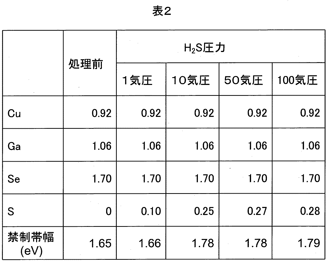
- Table 2 shows the chemical composition and band gap of the CuGaSe 2 thin film after treatment.
- the chemical composition is indicated by the coefficient of each element in the chemical formula of the film.
- Table 2 shows the chemical composition of the CuGaSe 2 thin film before treatment for comparison.
- the composition of the film before treatment is Cu 0.92 Ga 1.06 Se 1.70
- the film contains selenium atom defects.
- the selenium atom deficiency near the crystal grain surface is repaired by sulfur atoms, and the composition of the film becomes Cu 0.92 Ga 1.06 Se 1.70 S 0.10 .
- the selenium atom defects inside the crystal grains remained unrepaired, and the sum of the Se and S coefficients in the film chemical formula was 1.80.
- the film when the film was processed at a pressure of H 2 S gas of 10 atm, 50 atm, and 100 atm, sulfur atoms were introduced into selenium atom defects inside the crystal grains, and the composition of the film was Cu 0.92 Ga 1.06 Se x S y , and the value of x + y could be 1.95 or more and 2 or less.
- a selenium atom defect in a CuGaSe 2 crystal can be repaired with a sulfur atom, and a CuGaSeS thin film with few defects and close to the stoichiometric composition can be obtained.
- the Cu, Ga, and Se composition ratio of the film does not change even when the CuGaSe 2 film is processed.
- only selenium atom defect defects can be repaired with sulfur atoms without affecting these atoms.
- the forbidden band width of the CuGaSe 2 film treated by the method of the present invention is about 1.78 eV, which is larger than the forbidden band width (1.65 eV) of the film before the treatment.
- An AgInS 2 thin film was formed on a glass substrate using a known ternary co-evaporation method.
- the film thickness was 2 ⁇ m and the film was in a polycrystalline state.
- the thin film was processed using the apparatus of FIG. 1 and the processing scheme of FIG. The film is processed for 1 hour at a substrate temperature of 120 ° C and H 2 S gas pressure of 1, 10, 50, and 100 atmospheres, and the chemical composition and forbidden band width of the thin film obtained by processing at each pressure are determined. Examined.
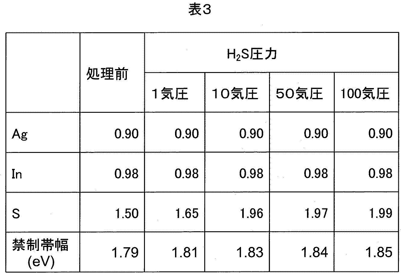
- Table 3 shows the chemical composition and band gap of the processed AgInS 2 thin film.
- the chemical composition is indicated by the coefficient of each element in the chemical formula of the film.
- Table 3 shows the chemical composition of the AgInS 2 thin film before treatment for comparison.
- the composition of the film before the treatment is Ag 0.90 In 0.98 S 1.50 , and the film contains sulfur atom defects.
- sulfur atom defects near the crystal grain surface were repaired by sulfur atoms, and the composition of the film became Ag 0.90 In 0.98 S 1.65 .
- the sulfur atom defects inside the crystal grains remained unrepaired, and the coefficient of S in the film chemical formula was 1.65.
- the film when the film was processed at a H 2 S gas pressure of 10 atm, 50 atm, and 100 atm, sulfur atoms were introduced into the sulfur atom defects inside the crystal grains, and the composition of the film was Ag 0.90 In 0.98 S x + y , and the value of x + y was 1.95 or more and 2 or less.
- sulfur atom defects in AgInS 2 crystals can be repaired by sulfur atoms.
- the present invention can repair only sulfur atom defects in the film with sulfur atoms without affecting the atoms present in the film before treatment.
- the forbidden band width of the AgInS 2 film processed by the method of the present invention is 1.83 to 1.85 eV, which is a larger value than the forbidden band width (1.79 eV) of the film before processing.
- the forbidden band width of the treated film is very close to 1.87 eV, which is the forbidden band width of AgInS 2 single crystal.
- a CuGaTe 2 thin film was formed on a glass substrate using a known ternary co-evaporation method.
- the film thickness was 2 ⁇ m and the film was in a polycrystalline state.
- the thin film was processed using the apparatus of FIG. 1 and the processing scheme of FIG. The film is processed for 1 hour at a substrate temperature of 120 ° C and H 2 S gas pressure of 1, 10, 50, and 100 atmospheres, and the chemical composition and forbidden band width of the thin film obtained by processing at each pressure are determined. Examined.
- Table 4 shows the chemical composition and band gap of the CuGaTe 2 thin film after treatment.
- the chemical composition is indicated by the coefficient of each element in the chemical formula of the film.
- Table 4 shows the chemical composition of the AgInS 2 thin film before treatment for comparison.
- the composition of the treated film is Cu 0.89 Ga 11.04 Te 1.65 , and the film contains sulfur atom defects.
- tellurium atom defects near the crystal grain surface were repaired by sulfur atoms, and the composition of the film became Cu 0.89 Ga 1.04 Te 1.65 S 0.12 .
- the composition ratio of Cu, Ga, and Te in the film does not change even when the CuGaTe 2 film is processed.
- the present invention can repair only the tellurium atom defects in the film with sulfur atoms without affecting the atoms present in the film before the treatment.
- the CuGaTe 2 film treated by the method of the present invention has a larger forbidden band width than the CuInTe 2 film before the treatment, and its value is from 1.42 to 1.43 eV. This forbidden bandwidth is very close to the forbidden bandwidth of 1.45 eV, which can convert sunlight into electrical energy most efficiently.
- a CuGaTe 2 thin film having an ideal forbidden bandwidth as a light absorption layer of a solar cell can be obtained.
- the CuGaTe 2 thin film treated according to the present invention has an advantage that it does not contain In which is a rare element, and is excellent in terms of element strategy.
- a CuAlSe 2 thin film was formed on a glass substrate using a known ternary co-evaporation method.
- the film thickness was 2 ⁇ m and the film was in a polycrystalline state.
- the thin film was processed using the apparatus of FIG. 1 and the processing scheme of FIG. The film is processed for 1 hour at a substrate temperature of 120 ° C and H 2 S gas pressure of 1, 10, 50, and 100 atmospheres, and the chemical composition and forbidden band width of the thin film obtained by processing at each pressure are determined. Examined.
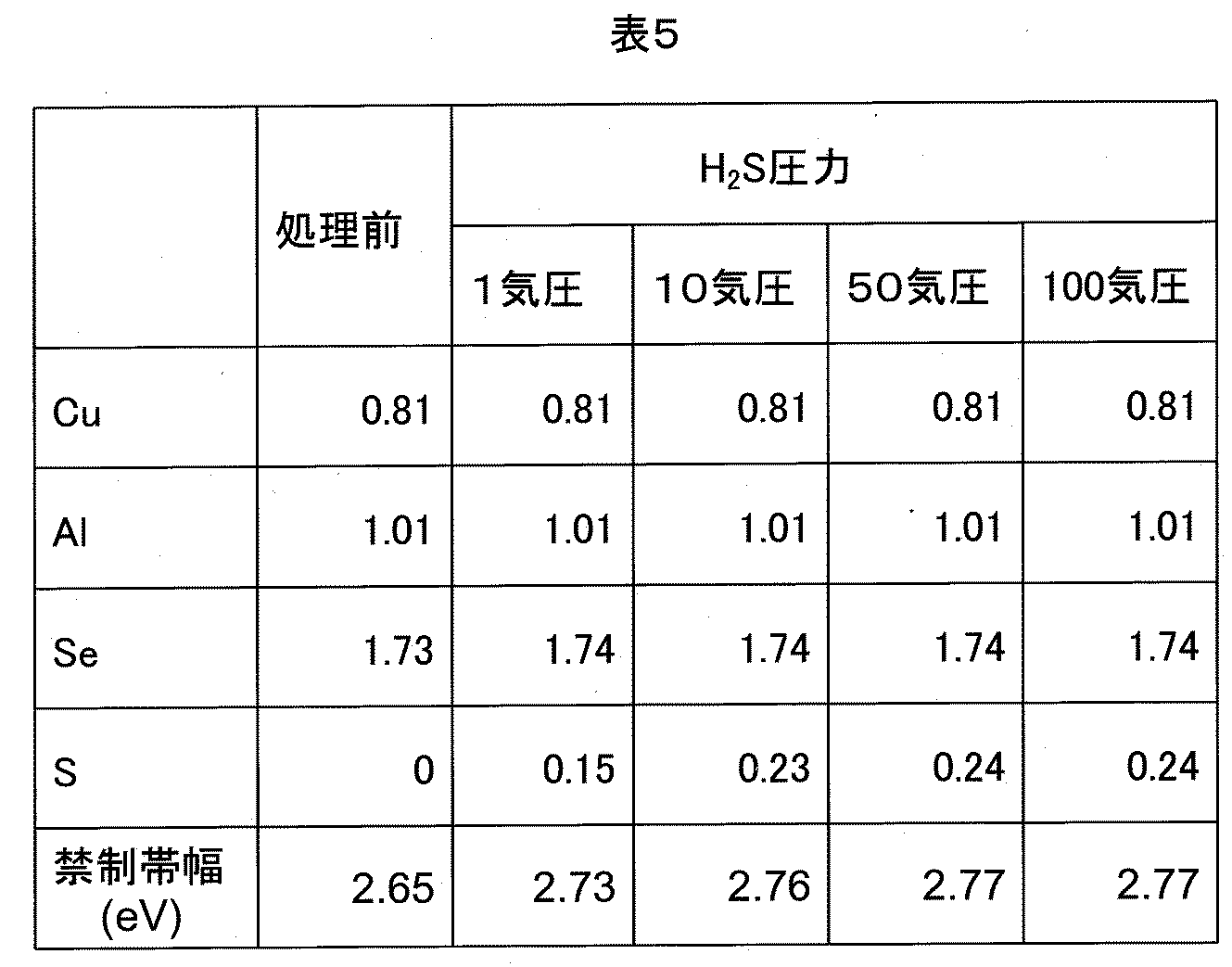
- Table 5 shows the chemical composition and band gap of the CuGaTe 2 thin film after treatment.
- the chemical composition is indicated by the coefficient of each element in the chemical formula of the film.
- the table shows the chemical composition of the CuAlSe 2 thin film before treatment for comparison.
- the composition of the treated film is Cu 0.81 Al 1.04 Se 1.73 , and the film contains sulfur atom defects.
- H 2 S gas atmosphere When the film was processed under a 1 atmosphere H 2 S gas atmosphere by a known technique, selenium atom defects near the crystal grain surface were repaired by sulfur atoms, and the composition of the film became Cu 0.81 Al 1.04 Se 1.73 S 0.15 .
- the film when the film was processed at a pressure of H 2 S gas of 10 atm, 50 atm, and 100 atm, sulfur atoms were introduced into tellurium atom defects inside the crystal grains, and the composition of the film was Cu 0.81 Al 1.04 Se x S y , and the value of x + y could be 1.95 or more and 2 or less.
- sulfur atom defects in CuAlSe 2 crystals can be repaired by sulfur atoms.
- the composition ratio of Cu, Al, and Se in the film does not change even when the CuAlSe 2 film is processed.
- the present invention can repair only selenium atom defects in the film with sulfur atoms without affecting the atoms present in the film before treatment.
- the CuAlSe 2 film treated by the method of the present invention has a larger forbidden band width than the CuAlSe 2 film before the treatment, and its value is 2.76 to 2.77 eV.
- the present invention can effectively repair chalcopyrite compound thin film defects with sulfur atoms.
- examples of repairing selenium and sulfur atom deficiency in CuInSe 2 , CuGaSe 2 , AgInS 2 and CuAlSe 2 thin films, and tellurium atom deficiency in CuGaTe 2 thin films were described, but other compositions having different compositions were used. The same effect can be obtained for a chalcopyrite compound thin film.
- the pressure of the pressurized sulfur gas is set to 10 atm or more and 100 atm or less, but the same effect can be obtained even when the gas pressure is set to 2 atm or more and less than 10 atm.
- the annealing time required to obtain a chalcopyrite compound thin film having a predetermined chemical composition becomes long.
- a chalcopyrite compound thin film having a predetermined chemical composition can be obtained by annealing for a relatively short time.
Landscapes
- Chemical & Material Sciences (AREA)
- Engineering & Computer Science (AREA)
- Chemical Kinetics & Catalysis (AREA)
- Materials Engineering (AREA)
- Mechanical Engineering (AREA)
- Metallurgy (AREA)
- Organic Chemistry (AREA)
- Physics & Mathematics (AREA)
- Thermal Sciences (AREA)
- Photovoltaic Devices (AREA)
- Manufacturing & Machinery (AREA)
Abstract
Description
y(t) = (2-x) -(2-x-y(0))exp(-kPt)
k:物質に依存する係数
P:圧力
と表せる。
2-(2-x-y(0))exp(-kPt) ≧1.95
より、
t≧-ln(0.05/2-x-y(0))/kP
となる。


2 不活性ガス源
3 不活性ガス配管
4 ガス加圧装置
5 硫黄ガス源
6 硫黄ガス配管
7 カルコパイライト薄膜
8 基板
9 薄膜ステージ
10 電気ヒーター
11 外部電源
12 電源ケーブル
13 電気スイッチ
14 CuInSe2製膜ステップ
15 結晶化ステップ
16 CuInSe2膜導入ステップ
17 窒素ガス導入ステップ
18 H2Sガス導入ステップ
19 セレン欠損処理ステップ
20 CuInSe2膜取り出しステップ
Claims (13)
- 基板上に、カルコパイライト化合物膜を製膜するステップと、
前記製膜したカルコパイライト化合物膜を、加圧条件下で、硫黄を含むガス雰囲気下でアニール処理するステップと、を有することを特徴とする半導体膜の製造方法。 - 前記カルコパイライト化合物は、化学式がXYZ2であり、Xは銀あるいは銅、Yはガリウム、インジウムあるいはアルミニウム、Zは硫黄、セレン、あるいはテルルであることを特徴とする請求項1記載の半導体膜の製造方法。
- 前記加圧条件は、2気圧以上100気圧以下であることを特徴とする請求項1の半導体膜の製造方法。
- 前記加圧条件は、10気圧以上100気圧以下であることを特徴とする請求項1の半導体膜の製造方法。
- 前記カルコパイライト化合物は、セレンまたは硫黄を含み、
前記アニール温度は、217℃よりも低く112℃よりも高いことを特徴とする請求項1の半導体膜の製造方法。 - 前記カルコパイライト化合物は、テルルを含み、
前記アニール温度は、449℃よりも低く112℃よりも高いことを特徴とする請求項1の半導体膜の製造方法。 - 前記硫黄を含むガスは、硫化水素ガスであることを特徴とする請求項1の半導体膜の製造方法。
- 前記アニール処理後のカルコパイライト化合物の化学式をXYZxSy(t)と表記し(tは時間)、
前記加圧条件下の圧力をPとすると、
前記アニール処理は、-ln(0.05/2-x-y(0))/kP(但し、kは物質に依存する係数)以上の時間行われることを特徴とする請求項1記載の半導体膜の製造方法。 - 前記アニール処理は、10分以上行われることを特徴とする請求項1記載の半導体膜の製造方法。
- 前記カルコパイライト化合物膜を製膜するステップの後、前記アニール処理するステップの前に、
カルコパイライト化合物膜の結晶化アニールを行うステップと、
アニール装置内に、不活性ガスを導入するステップと、を有することを特徴とする請求項1記載の半導体膜の製造方法。 - 基板と、
光吸収膜としてカルコパイライト化合物を有する太陽電池であって、
前記カルコパイライト化合物は、XYZxSy(Xは銀あるいは銅、Yはガリウム、インジウムあるいはアルミニウム、Zは硫黄、セレン、あるいはテルル、Sは硫黄)であり、x+yの値が1.95以上2以下であることを特徴とする太陽電池。 - 前記カルコパイライト化合物は、4元系以上であることを特徴とする請求項11記載の太陽電池。
- XYZxSy(Xは銀あるいは銅、Yはガリウム、インジウムあるいはアルミニウム、Zは硫黄、セレン、あるいはテルル、Sは硫黄)と表記されるカルコパイライト化合物であって、
x+yの値が1.95以上2以下であることを特徴とするカルコパイライト化合物。
Priority Applications (3)
| Application Number | Priority Date | Filing Date | Title |
|---|---|---|---|
| JP2014543094A JPWO2014064823A1 (ja) | 2012-10-26 | 2012-10-26 | 半導体膜の製造方法、太陽電池及びカルコパイライト化合物 |
| US14/436,886 US20150287853A1 (en) | 2012-10-26 | 2012-10-26 | Method for producing semiconductor film, solar cell, and chalcopyrite compound |
| PCT/JP2012/077675 WO2014064823A1 (ja) | 2012-10-26 | 2012-10-26 | 半導体膜の製造方法、太陽電池及びカルコパイライト化合物 |
Applications Claiming Priority (1)
| Application Number | Priority Date | Filing Date | Title |
|---|---|---|---|
| PCT/JP2012/077675 WO2014064823A1 (ja) | 2012-10-26 | 2012-10-26 | 半導体膜の製造方法、太陽電池及びカルコパイライト化合物 |
Publications (1)
| Publication Number | Publication Date |
|---|---|
| WO2014064823A1 true WO2014064823A1 (ja) | 2014-05-01 |
Family
ID=50544217
Family Applications (1)
| Application Number | Title | Priority Date | Filing Date |
|---|---|---|---|
| PCT/JP2012/077675 Ceased WO2014064823A1 (ja) | 2012-10-26 | 2012-10-26 | 半導体膜の製造方法、太陽電池及びカルコパイライト化合物 |
Country Status (3)
| Country | Link |
|---|---|
| US (1) | US20150287853A1 (ja) |
| JP (1) | JPWO2014064823A1 (ja) |
| WO (1) | WO2014064823A1 (ja) |
Cited By (3)
| Publication number | Priority date | Publication date | Assignee | Title |
|---|---|---|---|---|
| JP2015233139A (ja) * | 2014-06-10 | 2015-12-24 | エスケー イノベーション カンパニー リミテッドSk Innovation Co.,Ltd. | 原子層蒸着法で形成されたバッファ層を含む太陽電池、及び、その製造方法 |
| JP2017168753A (ja) * | 2016-03-17 | 2017-09-21 | 株式会社東芝 | 光電変換素子、光電変換素子モジュール、太陽電池及び太陽光発電システム |
| CN110518080A (zh) * | 2019-08-29 | 2019-11-29 | 无锡尚德太阳能电力有限公司 | 一种酸制绒多晶电池的返工方法 |
Families Citing this family (1)
| Publication number | Priority date | Publication date | Assignee | Title |
|---|---|---|---|---|
| CN113122224B (zh) * | 2019-12-30 | 2023-06-09 | Tcl科技集团股份有限公司 | 核壳结构的量子点及其制备方法和应用 |
Citations (3)
| Publication number | Priority date | Publication date | Assignee | Title |
|---|---|---|---|---|
| JP2000012883A (ja) * | 1998-06-25 | 2000-01-14 | Yazaki Corp | 太陽電池の製造方法 |
| JP2007503708A (ja) * | 2003-08-14 | 2007-02-22 | ユニヴァーシティ オブ ヨハネスバーグ | Ib−iiia−via族四元合金又は五元合金以上の合金から成る半導体薄膜を製造するための方法 |
| WO2011014245A2 (en) * | 2009-07-30 | 2011-02-03 | Oladeji Isaiah O | Method for fabricating copper-containing ternary and quaternary chalcogenide thin films |
Family Cites Families (1)
| Publication number | Priority date | Publication date | Assignee | Title |
|---|---|---|---|---|
| KR20120063324A (ko) * | 2010-12-07 | 2012-06-15 | 한국전자통신연구원 | 양면 태양전지 |
-
2012
- 2012-10-26 JP JP2014543094A patent/JPWO2014064823A1/ja active Pending
- 2012-10-26 WO PCT/JP2012/077675 patent/WO2014064823A1/ja not_active Ceased
- 2012-10-26 US US14/436,886 patent/US20150287853A1/en not_active Abandoned
Patent Citations (3)
| Publication number | Priority date | Publication date | Assignee | Title |
|---|---|---|---|---|
| JP2000012883A (ja) * | 1998-06-25 | 2000-01-14 | Yazaki Corp | 太陽電池の製造方法 |
| JP2007503708A (ja) * | 2003-08-14 | 2007-02-22 | ユニヴァーシティ オブ ヨハネスバーグ | Ib−iiia−via族四元合金又は五元合金以上の合金から成る半導体薄膜を製造するための方法 |
| WO2011014245A2 (en) * | 2009-07-30 | 2011-02-03 | Oladeji Isaiah O | Method for fabricating copper-containing ternary and quaternary chalcogenide thin films |
Cited By (4)
| Publication number | Priority date | Publication date | Assignee | Title |
|---|---|---|---|---|
| JP2015233139A (ja) * | 2014-06-10 | 2015-12-24 | エスケー イノベーション カンパニー リミテッドSk Innovation Co.,Ltd. | 原子層蒸着法で形成されたバッファ層を含む太陽電池、及び、その製造方法 |
| JP2017168753A (ja) * | 2016-03-17 | 2017-09-21 | 株式会社東芝 | 光電変換素子、光電変換素子モジュール、太陽電池及び太陽光発電システム |
| CN110518080A (zh) * | 2019-08-29 | 2019-11-29 | 无锡尚德太阳能电力有限公司 | 一种酸制绒多晶电池的返工方法 |
| CN110518080B (zh) * | 2019-08-29 | 2021-03-23 | 无锡尚德太阳能电力有限公司 | 一种酸制绒多晶电池的返工方法 |
Also Published As
| Publication number | Publication date |
|---|---|
| US20150287853A1 (en) | 2015-10-08 |
| JPWO2014064823A1 (ja) | 2016-09-05 |
Similar Documents
| Publication | Publication Date | Title |
|---|---|---|
| Shi et al. | Fabrication of Cu (In, Ga) Se2 thin films by sputtering from a single quaternary chalcogenide target | |
| CN102347398B (zh) | 大规模cigs基薄膜光伏材料的钠溅射掺杂方法 | |
| US8012546B2 (en) | Method and apparatus for producing semiconductor films and related devices | |
| US9087954B2 (en) | Method for producing the pentanary compound semiconductor CZTSSe, and thin-film solar cell | |
| JP4620105B2 (ja) | Cis系薄膜太陽電池の光吸収層の製造方法 | |
| JPWO2003005456A1 (ja) | 光吸収層の形成方法 | |
| CN102168252A (zh) | 用于大规模cigs基薄膜光伏材料的室内钠掺杂方法和系统 | |
| US20100248417A1 (en) | Method for producing chalcopyrite-type solar cell | |
| KR101628312B1 (ko) | CZTSSe계 박막 태양전지의 제조방법 및 이에 의해 제조된 CZTSSe계 박막 태양전지 | |
| CN104813482B (zh) | 用于cigs光伏器件的钼基材 | |
| CN101632154B (zh) | 利用一步金属有机化学气相沉积工艺制备ⅰ-ⅲ-ⅵ2化合物薄膜的方法 | |
| Zhang et al. | The effects of annealing temperature on CIGS solar cells by sputtering from quaternary target with Se-free post annealing | |
| Tsoulka et al. | Improved CuGaSe2 absorber properties through a modified co-evaporation process | |
| WO2014064823A1 (ja) | 半導体膜の製造方法、太陽電池及びカルコパイライト化合物 | |
| JP2004342678A (ja) | Cu(In1−xGax)Se2膜の製造方法及び太陽電池 | |
| CN114203842A (zh) | 宽禁带铜镓硒光吸收层及其制备方法、太阳能电池 | |
| JPH0555615A (ja) | 薄膜太陽電池の製造方法 | |
| KR101388458B1 (ko) | 급속 열처리 공정을 사용한 cigs 박막의 제조방법 | |
| CN107210187B (zh) | 用于生产用于具有硫化铟钠缓冲层的薄膜太阳能电池的层系统的方法 | |
| TW201421725A (zh) | 太陽能電池及其形成方法 | |
| RU2567191C1 (ru) | Способ изготовления фоточувствительных халькопиритных пленок | |
| JP5881987B2 (ja) | 太陽電池の製造方法 | |
| KR101521450B1 (ko) | CuSe2를 타겟으로 하는 비셀렌화 스퍼터링 공정을 이용한 CIGS 박막 제조방법 | |
| JP5904361B2 (ja) | Cis系薄膜太陽電池、及びその製造方法 | |
| TWI441344B (zh) | 光電轉換層的製造方法 |
Legal Events
| Date | Code | Title | Description |
|---|---|---|---|
| 121 | Ep: the epo has been informed by wipo that ep was designated in this application |
Ref document number: 12887196 Country of ref document: EP Kind code of ref document: A1 |
|
| ENP | Entry into the national phase |
Ref document number: 2014543094 Country of ref document: JP Kind code of ref document: A |
|
| WWE | Wipo information: entry into national phase |
Ref document number: 14436886 Country of ref document: US |
|
| NENP | Non-entry into the national phase |
Ref country code: DE |
|
| 122 | Ep: pct application non-entry in european phase |
Ref document number: 12887196 Country of ref document: EP Kind code of ref document: A1 |