WO2014061561A1 - 光電変換装置および光電変換装置の製造方法 - Google Patents
光電変換装置および光電変換装置の製造方法 Download PDFInfo
- Publication number
- WO2014061561A1 WO2014061561A1 PCT/JP2013/077648 JP2013077648W WO2014061561A1 WO 2014061561 A1 WO2014061561 A1 WO 2014061561A1 JP 2013077648 W JP2013077648 W JP 2013077648W WO 2014061561 A1 WO2014061561 A1 WO 2014061561A1
- Authority
- WO
- WIPO (PCT)
- Prior art keywords
- photoelectric conversion
- conversion device
- compound semiconductor
- layer
- composition
- Prior art date
- Legal status (The legal status is an assumption and is not a legal conclusion. Google has not performed a legal analysis and makes no representation as to the accuracy of the status listed.)
- Ceased
Links
Images





Classifications
-
- H—ELECTRICITY
- H10—SEMICONDUCTOR DEVICES; ELECTRIC SOLID-STATE DEVICES NOT OTHERWISE PROVIDED FOR
- H10F—INORGANIC SEMICONDUCTOR DEVICES SENSITIVE TO INFRARED RADIATION, LIGHT, ELECTROMAGNETIC RADIATION OF SHORTER WAVELENGTH OR CORPUSCULAR RADIATION
- H10F77/00—Constructional details of devices covered by this subclass
- H10F77/10—Semiconductor bodies
- H10F77/12—Active materials
- H10F77/126—Active materials comprising only Group I-III-VI chalcopyrite materials, e.g. CuInSe2, CuGaSe2 or CuInGaSe2 [CIGS]
-
- H—ELECTRICITY
- H10—SEMICONDUCTOR DEVICES; ELECTRIC SOLID-STATE DEVICES NOT OTHERWISE PROVIDED FOR
- H10F—INORGANIC SEMICONDUCTOR DEVICES SENSITIVE TO INFRARED RADIATION, LIGHT, ELECTROMAGNETIC RADIATION OF SHORTER WAVELENGTH OR CORPUSCULAR RADIATION
- H10F30/00—Individual radiation-sensitive semiconductor devices in which radiation controls the flow of current through the devices, e.g. photodetectors
- H10F30/20—Individual radiation-sensitive semiconductor devices in which radiation controls the flow of current through the devices, e.g. photodetectors the devices having potential barriers, e.g. phototransistors
-
- H—ELECTRICITY
- H10—SEMICONDUCTOR DEVICES; ELECTRIC SOLID-STATE DEVICES NOT OTHERWISE PROVIDED FOR
- H10F—INORGANIC SEMICONDUCTOR DEVICES SENSITIVE TO INFRARED RADIATION, LIGHT, ELECTROMAGNETIC RADIATION OF SHORTER WAVELENGTH OR CORPUSCULAR RADIATION
- H10F39/00—Integrated devices, or assemblies of multiple devices, comprising at least one element covered by group H10F30/00, e.g. radiation detectors comprising photodiode arrays
- H10F39/011—Manufacture or treatment of image sensors covered by group H10F39/12
- H10F39/021—Manufacture or treatment of image sensors covered by group H10F39/12 of image sensors having active layers comprising only Group III-V materials, e.g. GaAs, AlGaAs or InP
-
- H—ELECTRICITY
- H10—SEMICONDUCTOR DEVICES; ELECTRIC SOLID-STATE DEVICES NOT OTHERWISE PROVIDED FOR
- H10F—INORGANIC SEMICONDUCTOR DEVICES SENSITIVE TO INFRARED RADIATION, LIGHT, ELECTROMAGNETIC RADIATION OF SHORTER WAVELENGTH OR CORPUSCULAR RADIATION
- H10F39/00—Integrated devices, or assemblies of multiple devices, comprising at least one element covered by group H10F30/00, e.g. radiation detectors comprising photodiode arrays
- H10F39/10—Integrated devices
- H10F39/12—Image sensors
- H10F39/18—Complementary metal-oxide-semiconductor [CMOS] image sensors; Photodiode array image sensors
-
- H—ELECTRICITY
- H10—SEMICONDUCTOR DEVICES; ELECTRIC SOLID-STATE DEVICES NOT OTHERWISE PROVIDED FOR
- H10F—INORGANIC SEMICONDUCTOR DEVICES SENSITIVE TO INFRARED RADIATION, LIGHT, ELECTROMAGNETIC RADIATION OF SHORTER WAVELENGTH OR CORPUSCULAR RADIATION
- H10F39/00—Integrated devices, or assemblies of multiple devices, comprising at least one element covered by group H10F30/00, e.g. radiation detectors comprising photodiode arrays
- H10F39/10—Integrated devices
- H10F39/12—Image sensors
- H10F39/191—Photoconductor image sensors
-
- H—ELECTRICITY
- H10—SEMICONDUCTOR DEVICES; ELECTRIC SOLID-STATE DEVICES NOT OTHERWISE PROVIDED FOR
- H10F—INORGANIC SEMICONDUCTOR DEVICES SENSITIVE TO INFRARED RADIATION, LIGHT, ELECTROMAGNETIC RADIATION OF SHORTER WAVELENGTH OR CORPUSCULAR RADIATION
- H10F71/00—Manufacture or treatment of devices covered by this subclass
-
- H—ELECTRICITY
- H10—SEMICONDUCTOR DEVICES; ELECTRIC SOLID-STATE DEVICES NOT OTHERWISE PROVIDED FOR
- H10F—INORGANIC SEMICONDUCTOR DEVICES SENSITIVE TO INFRARED RADIATION, LIGHT, ELECTROMAGNETIC RADIATION OF SHORTER WAVELENGTH OR CORPUSCULAR RADIATION
- H10F77/00—Constructional details of devices covered by this subclass
- H10F77/10—Semiconductor bodies
- H10F77/16—Material structures, e.g. crystalline structures, film structures or crystal plane orientations
- H10F77/169—Thin semiconductor films on metallic or insulating substrates
- H10F77/1694—Thin semiconductor films on metallic or insulating substrates the films including Group I-III-VI materials, e.g. CIS or CIGS
-
- H—ELECTRICITY
- H10—SEMICONDUCTOR DEVICES; ELECTRIC SOLID-STATE DEVICES NOT OTHERWISE PROVIDED FOR
- H10F—INORGANIC SEMICONDUCTOR DEVICES SENSITIVE TO INFRARED RADIATION, LIGHT, ELECTROMAGNETIC RADIATION OF SHORTER WAVELENGTH OR CORPUSCULAR RADIATION
- H10F77/00—Constructional details of devices covered by this subclass
- H10F77/20—Electrodes
- H10F77/244—Electrodes made of transparent conductive layers, e.g. transparent conductive oxide [TCO] layers
-
- Y—GENERAL TAGGING OF NEW TECHNOLOGICAL DEVELOPMENTS; GENERAL TAGGING OF CROSS-SECTIONAL TECHNOLOGIES SPANNING OVER SEVERAL SECTIONS OF THE IPC; TECHNICAL SUBJECTS COVERED BY FORMER USPC CROSS-REFERENCE ART COLLECTIONS [XRACs] AND DIGESTS
- Y02—TECHNOLOGIES OR APPLICATIONS FOR MITIGATION OR ADAPTATION AGAINST CLIMATE CHANGE
- Y02E—REDUCTION OF GREENHOUSE GAS [GHG] EMISSIONS, RELATED TO ENERGY GENERATION, TRANSMISSION OR DISTRIBUTION
- Y02E10/00—Energy generation through renewable energy sources
- Y02E10/50—Photovoltaic [PV] energy
- Y02E10/541—CuInSe2 material PV cells
-
- Y—GENERAL TAGGING OF NEW TECHNOLOGICAL DEVELOPMENTS; GENERAL TAGGING OF CROSS-SECTIONAL TECHNOLOGIES SPANNING OVER SEVERAL SECTIONS OF THE IPC; TECHNICAL SUBJECTS COVERED BY FORMER USPC CROSS-REFERENCE ART COLLECTIONS [XRACs] AND DIGESTS
- Y02—TECHNOLOGIES OR APPLICATIONS FOR MITIGATION OR ADAPTATION AGAINST CLIMATE CHANGE
- Y02E—REDUCTION OF GREENHOUSE GAS [GHG] EMISSIONS, RELATED TO ENERGY GENERATION, TRANSMISSION OR DISTRIBUTION
- Y02E10/00—Energy generation through renewable energy sources
- Y02E10/50—Photovoltaic [PV] energy
- Y02E10/543—Solar cells from Group II-VI materials
-
- Y—GENERAL TAGGING OF NEW TECHNOLOGICAL DEVELOPMENTS; GENERAL TAGGING OF CROSS-SECTIONAL TECHNOLOGIES SPANNING OVER SEVERAL SECTIONS OF THE IPC; TECHNICAL SUBJECTS COVERED BY FORMER USPC CROSS-REFERENCE ART COLLECTIONS [XRACs] AND DIGESTS
- Y02—TECHNOLOGIES OR APPLICATIONS FOR MITIGATION OR ADAPTATION AGAINST CLIMATE CHANGE
- Y02P—CLIMATE CHANGE MITIGATION TECHNOLOGIES IN THE PRODUCTION OR PROCESSING OF GOODS
- Y02P70/00—Climate change mitigation technologies in the production process for final industrial or consumer products
- Y02P70/50—Manufacturing or production processes characterised by the final manufactured product
Definitions
- the present invention relates to a photoelectric conversion device having a CIGS compound semiconductor layer and a method for manufacturing the photoelectric conversion device.
- Patent Document 1 discloses that an electrode of a molybdenum (Mo) layer formed on a substrate of soda lime glass (SLG) by sputtering, a photoelectric conversion layer by a Cu (In 1-x Ga x ) Se 2 film, or Disclosed is a solar cell having a light absorption layer, a buffer layer made of a CdS layer formed by a solution growth method, a window layer made of ZnO deposited by MOCVD method, and finally an electrode made of aluminum deposited or sputtered and patterned Yes.
- Mo molybdenum
- an In—Ga—Se film is deposited on a substrate, and then Cu—Se is supplied to the In—Ga—Se film under heating to convert In—Ga—Se to Cu—Se-excess Cu (In 1-x Ga x) into a Se 2 film, further the Cu (in 1-x Ga x ) by supplying an in-Ga-Se in Se 2 film excess Cu-Se Cu (in 1- x Ga x ) Se 2 is converted into a Cu (In 1-x Ga x ) Se 2 (0 ⁇ x ⁇ 1) film on the substrate, and then formed on the surface of the Cu (In 1-x Ga x ) Se 2 film. It is formed using a so-called three-stage method that further includes a step of removing the remaining Cu—Se-based compound.
- a CIGS (CuInGaSe) -based compound semiconductor has a lower band gap as its composition approaches that of a CIS (CuInSe) -based compound semiconductor. Thereby, it is possible to increase the wavelength of sensitivity, but conversely, the dark current increases. On the other hand, when the composition is close to that of a CGS (CuGaSe) -based compound semiconductor, the band gap is increased and sensitivity is not obtained in a long wavelength band, but the dark current can be reduced.
- composition structure close to CIS and CGS can coexist in the CIGS compound semiconductor, it is considered that the sensitivity can be increased in wavelength and the dark current can be reduced.
- An object of the present invention is to provide a photoelectric conversion device and a method for manufacturing the photoelectric conversion device that can achieve both a longer wavelength of sensitivity and a reduction in dark current.
- the photoelectric conversion device of the present invention includes a substrate, a lower electrode layer disposed on the substrate, a CIGS compound semiconductor layer disposed on the lower electrode layer so as to cover the lower electrode layer, and the compound A transparent electrode layer disposed on the semiconductor layer, wherein the compound semiconductor layer has a maximum Ga compositional difference of 5% or more and a maximum In compositional difference of 6% or more in the layer thickness direction. is there.
- CIS and CGS or a composition structure close to these can coexist in the CIGS compound semiconductor layer.
- the sensitivity can be increased in wavelength by the composition structure close to CIS or CIS, and the dark current can be reduced by the composition structure close to CGS or CGS. That is, it is possible to achieve both a longer wavelength of sensitivity and a characteristic of reducing dark current.
- the compound semiconductor layer includes an intermediate portion having a larger In composition than a Ga composition, and an end portion disposed on the upper side and / or lower side of the intermediate portion in the layer thickness direction and having a larger Ga composition than the In composition. Is preferred.
- the difference between the Ga composition at the end portion and the Ga composition at the intermediate portion is 5% or more, and the difference between the In composition at the intermediate portion and the Ga composition at the end portion is 6% or more. There may be.
- the intermediate part preferably has an In composition of 14 at% to 20 at% and a Ga composition of 0 at% to 4 at%.
- the Ga composition ratio (Ga / Ga + In) to the total amount of Ga and In in the intermediate portion is 0 to 0.17
- the In composition ratio (In / Ga + In) to the total amount is 0.83 to 1. It is preferable.
- the end portion preferably has a Ga composition of 6 at% to 15 at% and an In composition of 0 at% to 8 at%.
- the Ga composition ratio (Ga / Ga + In) to the total amount of Ga and In at the end is 0.65 to 1, and the In composition ratio (In / Ga + In) to the total amount is 0 to 0.35. It is preferable.
- the absorption wavelength of the compound semiconductor layer preferably includes a range of 1200 nm or more.
- the lower electrode layer includes a plurality of lower electrode layers arranged at intervals, and the compound semiconductor layer is disposed on the lower electrode layer so as to collectively cover the plurality of lower electrode layers, A compound semiconductor layer partitioned into a plurality of pixels may be included.
- the photoelectric conversion device can be used as an image sensor.
- the lower electrode layer may be a single lower electrode layer.
- the photoelectric conversion device can be used as a solar cell.
- the photoelectric conversion device may include a circuit unit disposed between the substrate and the lower electrode layer.
- the circuit unit may include a CMOS field effect transistor.
- the CMOS field effect transistor may include a source layer and a drain layer selectively formed on the surface portion of the substrate, and a gate electrode disposed between the source layer and the drain layer.
- the transparent electrode layer may be made of zinc oxide (ZnO) or indium tin oxide (ITO).
- the photoelectric conversion device may include a buffer layer disposed between the compound semiconductor layer and the transparent electrode layer.
- the buffer layer, CdS, ZnS, ZnO may consist (Zn z Mg 1-z) O (0 ⁇ z ⁇ 1), ZnSe or In 2 S 3.
- the method for manufacturing a photoelectric conversion device includes a step of forming a lower electrode layer on a substrate, a step of forming a CIGS-based compound semiconductor layer so as to cover the lower electrode layer, and a step on the compound semiconductor layer.
- the step of forming the compound semiconductor layer includes a Ga surplus supply step of supplying more Ga than In, a Cu supply step of supplying Cu, and an In than Ga In excess supply steps for supplying a large amount of In, by performing these steps, the Ga composition difference in the layer thickness direction of the compound semiconductor layer becomes 5% or more at the maximum, and the In composition difference in the layer thickness direction Including a step of forming the compound semiconductor layer so that the maximum is 6% or more.
- CIS and CGS or a composition structure close to these can coexist in the CIGS compound semiconductor layer.
- the sensitivity can be increased by the CIS or the composition structure close to CIS, and the dark current can be reduced by the composition structure close to CGS or CGS. That is, it is possible to achieve both a longer wavelength of sensitivity and a characteristic of reducing dark current.
- the Ga surplus supply step is first performed, and then the In surplus supply step and the Cu supply step are performed in this order.
- the In surplus supply step and the Ga surplus supply step are further performed in this order following the Cu supply step.
- the step of forming the compound semiconductor layer it is preferable to finish the step in the Ga surplus supply step.
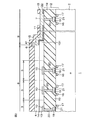
- FIG. 1 is a schematic plan view of the photoelectric conversion device according to the first embodiment of the present invention.
- FIG. 2 is a cross-sectional view taken along section line II-II in FIG.
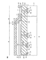
- FIG. 3 is a schematic cross-sectional view of a photoelectric conversion device according to the second embodiment of the present invention.
- FIG. 4 is a flowchart for explaining an example of the manufacturing process of the photoelectric conversion device.
- FIG. 5 is a time chart for explaining a process related to formation of the compound semiconductor layer.
- FIG. 6 is a list of examples of process variations related to the formation of the compound semiconductor layer.
- FIG. 7 is a graph showing the relationship between the thickness of the compound semiconductor layer and the atomic concentration of each element.
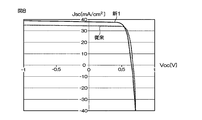
- FIG. 8 is a graph showing the JV characteristics of the photoelectric conversion device.
- FIG. 9 is a graph showing various characteristics of the solar cell of the photoelectric conversion device.
- 10A to 10C are graphs showing the relationship between the wavelength and the quantum efficiency of the photoelectric conversion device.
- FIG. 1 is a schematic plan view of the photoelectric conversion device according to the first embodiment of the present invention.
- the photoelectric conversion device 1 is an image sensor that detects incident light and converts light energy into an electrical signal.
- the photoelectric conversion device 1 may be used as a line image sensor by arranging a plurality of one-dimensionally, or may be used as an area image sensor by arranging a plurality of two-dimensionally.
- the photoelectric conversion device 1 performs personal authentication with a security camera (a camera that senses visible light during the day and a near-infrared light at night) and a personal authentication camera (a near-infrared light that is not affected by outside light).
- the present invention can be applied to a photodetector in the wavelength band (photodetector), an avalanche photodiode, and the like. Furthermore, you may apply the photoelectric conversion apparatus 1 to a solar cell.
- the photoelectric conversion device 1 includes a substrate 2, a plurality of pixels 3, a transparent electrode layer 4, a metal electrode layer 6, and a plurality of pads 7.
- the substrate 2 is made of, for example, silicon (Si).
- the substrate 2 has a size of 5 mm to 10 mm square, for example.
- a light receiving region 8 is formed at the center of the substrate 2 and a peripheral region 9 is formed so as to surround the light receiving region 8.
- the substrate 2 has a thickness of 400 ⁇ m to 1000 ⁇ m, for example.
- substrate 2 may consist of a blue plate glass (SLG). In that case, the substrate 2 preferably has a size of 50 cm ⁇ 100 cm square and a thickness of 2 mm.
- the plurality of pixels 3 are arranged in a matrix (matrix) in the light receiving region 8.
- Each pixel 3 is provided with one lower electrode layer 10.
- the transparent electrode layer 4 is disposed on the pixels 3 so as to cover the matrix-like pixels 3 collectively.
- the metal electrode layer 6 is made of, for example, aluminum (Al).
- the metal electrode layer 6 is formed in an annular shape surrounding the transparent electrode layer 4 in the peripheral region 9 and covers the peripheral edge 41 of the transparent electrode layer 4. Thereby, the metal electrode layer 6 is connected to the peripheral edge portion 41 of the transparent electrode layer 4.
- the plurality of pads 7 are arranged at intervals from each other in a region spaced from the metal electrode layer 6. In this embodiment, the plurality of pads 7 are arranged linearly along each side of the substrate 2. Some (or one or more) of the plurality of pads 7 may be connected to the metal electrode layer 6 through a pad connection portion 11 formed integrally with the metal electrode layer 6. Has been. The pad connection portion 11 is formed across the pad 7 and the metal electrode layer 6.
- FIG. 2 is a cross-sectional view taken along the section line II-II in FIG.
- the photoelectric conversion device 1 includes a circuit unit 12, a lower electrode layer 10, a compound semiconductor layer 13, a buffer layer 14, a transparent electrode layer 4, a metal electrode layer 6, and a surface protective film 15 that are sequentially stacked on the substrate 2.
- the circuit unit 12 includes, for example, a CMOS field effect transistor.
- the circuit unit 12 shows a plurality of n-channel MOS transistors that constitute a part of the CMOS field effect transistor.
- the n-channel MOS transistor includes a source layer 16 and a drain layer 17 selectively formed on the surface of the substrate 2, a gate electrode 18 disposed between the source layer 16 and the drain layer 17, and a substrate 2.
- An interlayer film 19 formed to cover the gate electrode 18 and a via electrode 20 penetrating the interlayer film 19 are included.
- a gate insulating film 21 is disposed between the gate electrode 18 and the substrate 2.
- the via electrodes 20 may connect the lower electrode layer 10 and the gate electrode 18. Since the lower electrode layer 10 (anode) is connected to the gate electrode 18, the optical information (electric signal) detected by the compound semiconductor layer 13 is amplified by the n-channel MOS transistor. The remaining via electrode 20 (one or plural) may connect the pad 7 and the gate electrode 18. Thereby, the metal electrode layer 6 is electrically connected to the circuit unit 12 in the peripheral region 9.
- the configuration of the circuit unit 12 illustrated in FIG. 2 is merely an example.
- the circuit unit 12 may be a thin film transistor having a CMOS structure formed on a thin film on a glass substrate.
- the lower electrode layer 10 is made of, for example, molybdenum (Mo), niobium (Nb), tantalum (Ta), or tungsten (W). Of these, tungsten (W) is preferred. Since tungsten (W) has a higher reflectance than other materials, not only the light incident on the compound semiconductor layer 13 but also the light reflected by the lower electrode layer 10 can be detected by the compound semiconductor layer 13. Further, since tungsten (W) can be easily processed using LSI manufacturing technology, the size of the lower electrode layer 10 can be easily controlled.
- Mo molybdenum
- Nb niobium
- Ta tantalum
- tungsten (W) is preferred. Since tungsten (W) has a higher reflectance than other materials, not only the light incident on the compound semiconductor layer 13 but also the light reflected by the lower electrode layer 10 can be detected by the compound semiconductor layer 13. Further, since tungsten (W) can be easily processed using LSI manufacturing technology, the size of the lower electrode layer 10 can be easily controlled.
- the compound semiconductor layer 13 is formed so as to collectively cover the plurality of lower electrode layers 10, and is partitioned into a plurality of pixels 3.
- the compound semiconductor layer 13 preferably has a thickness of 0.1 ⁇ m to 2 ⁇ m, and specifically, preferably has a thickness of about 1.0 ⁇ m. Moreover, when applying the photoelectric conversion apparatus 1 to a solar cell, it is preferable that the compound semiconductor layer 13 has a thickness of about 1.8 ⁇ m.
- the compound semiconductor layer 13 is made of a CIGS semiconductor represented by Cu y (In x Ga 1-x ) Se 2 (0 ⁇ y ⁇ 1, 0 ⁇ x ⁇ 1). A specific composition structure of the compound semiconductor layer 13 will be described in detail later.
- the buffer layer 14 is formed so as to cover almost the entire upper surface of the compound semiconductor layer 13.
- the peripheral edge 131 of the compound semiconductor layer 13 is not covered with the buffer layer 14, and is drawn from the buffer layer 14 in the lateral direction along the surface of the substrate 2.
- An insulating film 22 is formed so as to cover the peripheral portion 131 (upper surface and side surface) of the compound semiconductor layer 13 and the upper surface of the surrounding interlayer film 19.
- the buffer layer 14 has a thickness of 100 to 10,000 mm, for example.
- Buffer layer 14, CdS, ZnS, ZnO be made of (Zn z Mg 1-z) O (0 ⁇ z ⁇ 1), ZnSe or an In 2 S 3 preferred.
- the transparent electrode layer 4 is formed so as to cover the entire upper surface of the buffer layer 14.
- the transparent electrode layer 4 has a thickness of 100 to 10,000 mm, for example.
- the transparent electrode layer 4 is preferably made of zinc oxide (ZnO).
- ZnO zinc oxide
- i-ZnO non-doped ZnO film
- n-ZnO n-type ZnO film
- the transparent electrode layer 4 may be indium tin oxide (ITO).
- the metal electrode layer 6 is formed on the laminated structure of the compound semiconductor layer 13, the buffer layer 14, and the transparent electrode layer 4, and the top portion covers the peripheral edge 41 (upper surface and side surface) of the transparent electrode layer 4.
- the metal electrode layer 6 and the compound semiconductor layer 13 and the buffer layer 14 are insulated from each other by the insulating film 22.
- the lower part of the metal electrode layer 6 is disposed on the interlayer film 19 in the lateral direction along the surface of the substrate 2 and is connected to the pad 7 via the pad connection part 11.
- the surface protective film 15 is made of an insulating material such as silicon nitride (Si 3 N 4 ), for example.
- the surface protective film 15 is formed so as to cover the metal electrode layer 6, the pad connection portion 11, and the pad 7.
- the metal electrode layer 6 is completely covered with the surface protective film 15 so as not to be exposed. Further, a part of the pad 7 is selectively exposed from the opening formed in the surface protective film 15.
- FIG. 3 is a schematic cross-sectional view of a photoelectric conversion device according to the second embodiment of the present invention. 3, parts corresponding to those shown in FIG. 2 described above are shown with the same reference numerals.
- the photoelectric conversion device 1 of the first embodiment one lower electrode layer 10 is provided corresponding to each pixel 3, and a plurality of lower electrode layers 10 are arranged in a matrix as a whole.
- the photoelectric conversion device 5 of the second embodiment includes a single lower electrode layer 23 formed on the interlayer film 19. Therefore, the compound semiconductor layer 13 covering the lower electrode layer 23 is not partitioned into a plurality of pixels.
- the photoelectric conversion device 5 having such a structure is suitable for use as a solar cell.
- FIG. 4 is a flowchart for explaining an example of the manufacturing process of the photoelectric conversion device 1.
- FIG. 5 is a time chart for explaining a process related to the formation of the compound semiconductor layer 13.
- CMOS field effect transistor is formed on the substrate 2 (step S1).
- an interlayer film 19 is formed on the substrate 2 by a CVD (Chemical Vapor Deposition) method, and a via electrode 20 that penetrates the interlayer film 19 and reaches the gate electrode 18 is formed (step S2).
- Mo molybdenum
- sputtering for example, and then the molybdenum is patterned (etched) to form a plurality of lower electrode layers 10 in a matrix (see FIG. Step S3).
- the next step is a step of forming the compound semiconductor layer 13 (step S4).
- the first step to the fifth step are sequentially executed by the MBE (Molecular Beam Epitaxy) method (five-step method), and the step is completed with the fifth step.
- the film forming temperature is 350 ° C. to 600 ° C.
- Se is always supplied at a constant amount (for example, Se flux of 1 ⁇ 10 3 Pa to 5 ⁇ 10 3 Pa) throughout all the steps.
- the first step is a Ga surplus supply step for supplying more Ga than In.
- the flux ratio of Ga to In (Ga / In) is controlled in the range of 1 to ⁇ , for example.
- the first step ends when the film is deposited by about 0.2 ⁇ m to 0.3 ⁇ m (time is about 2200 seconds to 3960 seconds).
- the second step is an In surplus supply step for supplying more In than Ga.
- the flux ratio of In to Ga (In / Ga) is controlled in the range of 1 to ⁇ , for example. Then, the second step ends when the film is deposited by about 0.2 ⁇ m to 0.3 ⁇ m (time is about 3000 seconds to 5400 seconds).
- the third step is a Cu supply step for supplying Cu.
- the supplied Cu diffuses into the already deposited Ga film and In film, and together with the respective elements, a composition structure close to CGS (CuGaSe) and a composition structure close to CIS (CuInSe) are obtained.
- the third step is the time when the composition ratio (Cu / III) of Cu to Ga and In (collectively these group IIIB elements) reaches about 1.2 (time is about 1800 seconds to 3240 seconds). End with.
- the composition ratio (Cu / III) serving as an indication of the termination can be determined by, for example, the temperature change of the substrate 2. For example, the time when the temperature of the substrate 2 drops by about 0.01 ° C. to 1 ° C. may be set as the time when Cu / III becomes 1.0.
- the fourth step is an In surplus supply step similar to the second step.
- the flux ratio (In / Ga) in the fourth step may be the same as in the second step.
- the fourth step ends when the film is deposited by about 0.1 ⁇ m to 0.15 ⁇ m (time is about 1500 seconds to 2700 seconds).
- the fifth step is a Ga surplus supply step similar to the first step.
- the flux ratio (Ga / In) in the fifth step may be the same as that in the first step.
- the fifth step ends when the film is deposited by about 0.1 ⁇ m to 0.15 ⁇ m (time is about 1100 seconds to 1980 seconds).
- the compound semiconductor layer 13 is formed through the above five steps. Note that Cu diffuses also in the In film and Ga film deposited in the fourth step and the fifth step after the Cu supply step (third step), and together with each element, a composition structure close to CGS and a composition close to CIS. Form a structure. Therefore, at the end of the fifth step, the composition ratio (Cu / III) in the compound semiconductor layer 13 is about 0.6 to 0.9.
- the method of forming the compound semiconductor layer 13 is not limited to the five-step method described above, and various methods can be employed within the scope of the present invention. A list of examples of adoptable methods is shown in FIG.
- FIG. 6 is a list of variations of the formation process of the compound semiconductor layer 13.
- “new 1 (process shown in FIG. 5)” to “new 9” are shown as variations of the present invention in the horizontal direction, and “conventional” is shown as a conventional example.
- the order of the raw material supply steps when forming the compound semiconductor layer 13 is described in the vertical direction. Note that the lower side in FIG. 6 is the side closer to the lower electrode layer 10, and the upper side is the side closer to the buffer layer 14.
- the numerical value next to each raw material supply step indicates the depth ( ⁇ m) from the surface of the compound semiconductor layer 13.
- the meaning of the abbreviation of the raw material step in FIG. 6 is a step where “GaIn” supplies Ga and In at a film forming rate ratio (Ga / In) of 0.3 to 0.6, and “Cu” In the Cu supply step, “Ga” is the Ga surplus supply step, and “In” is the In surplus supply step.
- the compound semiconductor layer 13 is formed by a three-stage method in which a GaIn supply step, a Cu supply step, and a GaIn supply step are sequentially performed.
- a Ga surplus supply step, an In surplus supply step, a Cu supply step, a G surplus supply step, and an In surplus supply step are sequentially executed.
- a Ga surplus supply step The compound semiconductor layer 13 is formed by a four-stage method in which the In surplus supply step, the Cu supply step, and the GaIn supply step are sequentially performed.
- the buffer layer 14 and the transparent electrode layer 4 are sequentially laminated by, for example, the CVD method. These are patterned at once (steps S5 and S6).
- the metal electrode layer 6 is formed, for example, by sputtering (step S7), and the surface protective film 15 is formed, for example, by CVD (step S8).
- FIG. 7 is a graph showing the relationship between the thickness of the compound semiconductor layer 13 (CIGS thickness) and the atomic concentration of each element.
- FIG. 7 compares the difference in atomic concentration (composition difference) between Ga and In between “new 1” and “conventional” in FIG.
- the Ga atom concentration in the thickness direction of the compound semiconductor layer 13 (Ga composition ratio in the compound semiconductor layer 13).
- the In atom concentration (In composition ratio in the compound semiconductor layer 13) does not change much.
- the difference (composition difference) between the maximum value and the minimum value of the Ga atom concentration is about 4%
- the difference between the maximum value and the minimum value of the In atom concentration is about 5%.
- the compositional difference in Ga atom concentration is 5% or more at the maximum, and the compositional difference in In atom concentration is 6% or more. It was.
- the In atom concentration significantly exceeds the Ga atom concentration in the intermediate portion 24 of the compound semiconductor layer 13 having a thickness of 0.2 ⁇ m to 1.2 ⁇ m.
- the In atom concentration in the intermediate portion 24 is 11 at% to 16 at%, whereas the Ga atom concentration is only 1 at% to 5 at%.
- This atomic concentration is a ratio to the total amount of atoms contained in the compound semiconductor layer 13 containing Cu, Se, or the like. Therefore, when the composition ratio of Ga and In to the total amount of Ga and In in the intermediate portion 24 is calculated, the Ga composition ratio (Ga / Ga + In) is 0.08 to 0.24, and the In composition ratio (In / Ga + In) is 0.76 to 0.92.
- the Ga composition ratio (Ga / Ga + In) and the In composition ratio (In / Ga + In) are numerical values defined excluding the amounts of Cu and Se. Therefore, as the composition of Cu and Se varies, the composition ratio of Ga and In to the total atomic amount of the compound semiconductor layer 13 varies, but the composition ratio of Ga (Ga / Ga + In) and the composition ratio of In (In / Ga + In ) Is held constant.
- the Ga atom concentration is In atoms. Concentration is significantly above. Specifically, the Ga atom concentration in the lower end portion 25 and the upper end portion 26 is 7 at% to 10 at%, whereas the In atom concentration is only 2 at% to 9 at%.
- the Ga composition ratio (Ga / Ga + In) is 0.53 to The In composition ratio (In / Ga + In) is 0.22 to 0.47.
- composition difference in Ga atom concentration between the intermediate portion 24, the lower end portion 25, and the upper end portion 26 is the maximum composition difference (about 8.5%) in the compound semiconductor layer 13. Further, the composition difference in In atom concentration between the intermediate portion 24 and the lower end portion 25 and the upper end portion 26 is the maximum composition difference (about 14.5%) in the compound semiconductor layer 13.
- FIG. 8 is a graph showing the JV characteristics of the photoelectric conversion device 1.
- “New 1” and “Conventional” in FIG. 6 are compared with respect to JV characteristics when the photoelectric conversion device 1 is used as a solar cell.
- “New 1” with relatively large Ga and In gratings can exhibit superior JV characteristics as compared with “Conventional”.
- FIG. 9 is a graph showing various characteristics of the solar cell of the photoelectric conversion device 1.
- “new 1” and “new 5” in FIG. 6 and “conventional” in FIG. 6 are compared with respect to various characteristics when the photoelectric conversion device 1 is used as a solar cell.
- 10 (a) to 10 (c) are graphs showing the relationship between the wavelength and the quantum efficiency of the photoelectric conversion device.
- 10 (a) to 10 (c) regarding the increase in wavelength when the photoelectric conversion device 1 is used as a solar cell, “new 1”, “new 2” and “new 5” in FIG. Were compared.
- 10A shows a comparison between “New 1” and “Conventional”
- FIG. 10B shows a comparison between “New 2” and “Conventional”
- FIG. 10C shows “New 5”. And comparison with “conventional”.
- “new 1”, “new 2”, and “new 5” with relatively large Ga and In gratings have spectral sensitivities from 1200 nm as compared with “conventional”. It was found that the wavelength could be increased to 1300 nm. That is, according to FIGS. 10A to 10C, by increasing the Ga and In gratings in the compound semiconductor layer 13, the compound semiconductor layer 13 has a composition structure close to CIS or CIS. It was found that the spectral sensitivity was longer.
- FIG. 11 is a graph showing the dark current characteristics of the photoelectric conversion device 1.
- “new 5” and “conventional” in FIG. 6 are compared with respect to dark current characteristics when the photoelectric conversion device 1 is used as an image sensor.
- “new 5” having relatively large Ga and In gratings can reduce dark current compared to “conventional”. That is, according to FIG. 11, by increasing the Ga and In gratings in the compound semiconductor layer 13, the compound semiconductor layer 13 has CGS or a composition structure close to CGS, and the dark current is reduced by the structure. I understood it.
- the dark current can be further reduced by controlling the order and number of Ga surplus supply steps when forming the compound semiconductor layer 13 by the multi-step method.
- the CIGS-based compound semiconductor layer 13 can coexist with CIS and CGS, or a composition structure close thereto. I was able to prove. For this reason, the sensitivity can be increased by the wavelength by the composition structure close to CIS or CIS (see FIG. 10), and the dark current can be reduced by the composition structure close to CGS or CGS (see FIG. 11). That is, it is possible to achieve both a longer wavelength of sensitivity and a characteristic of reducing dark current.
- circuit elements such as capacitors and resistors may be formed on the substrate 2 in addition to CMOS field effect transistors.
- These circuit elements also enable integrated circuits such as SSI (Small Scale Scale Integration), MSI (Medium Scale Scale Integration), LSI (Large Scale Scale Integration), VLSI (Very Large Scale Scale Integration), and ULSI (Ultra-Very Large Scale Scale Integration). May be configured.
Landscapes
- Photovoltaic Devices (AREA)
- Light Receiving Elements (AREA)
- Solid State Image Pick-Up Elements (AREA)
- Engineering & Computer Science (AREA)
- Manufacturing & Machinery (AREA)
Abstract
本発明の光電変換装置は、基板と、前記基板上に配置された下部電極層と、前記下部電極層を覆うように前記下部電極層上に配置されたCIGS系の化合物半導体層と、前記化合物半導体層上に配置された透明電極層とを含み、前記化合物半導体層の層厚方向のGaの組成差が最大5%以上であり、前記層厚方向のInの組成差が最大6%以上である。
Description
本発明は、CIGS系の化合物半導体層を有する光電変換装置およびその製造方法に関する。
従来、CIGS系半導体を用いた光電変換装置が公知である。たとえば、特許文献1は、ソーダライムガラス(SLG)の基板上に、順に、スパッタで形成されたモリブデン(Mo)層の電極、Cu(In1-xGax)Se2膜による光電変換層または光吸収層、溶液成長法で形成したCdS層からなるバッファ層、さらにMOCVD法で堆積したZnOからなる窓層、最後に蒸着またはスパッタおよびパターニングしたアルミニウムからなる電極を有する、太陽電池を開示している。
光電変換層は、基板上にIn-Ga-Se膜を堆積し、次いで加熱下でIn-Ga-Se膜にCu-Seを供給してIn-Ga-SeをCu-Se過剰のCu(In1-xGax)Se2膜に変換し、さらに当該Cu(In1-xGax)Se2膜にIn-Ga-Seを供給して過剰のCu-SeをCu(In1-xGax)Se2に変換して基板上にCu(In1-xGax)Se2(0<x≦1)膜を形成した後、Cu(In1-xGax)Se2膜の表面に残存するCu-Se系化合物を除去する工程をさらに有する、いわゆる3段階法を用いて形成される。
CIGS(CuInGaSe)系化合物半導体は、その組成がCIS(CuInSe)系化合物半導体に近づくにしたがって、バンドギャップが低くなる。これにより、感度の長波長化を図ることができるが、逆に、暗電流が高くなる。一方、その組成をCGS(CuGaSe)系化合物半導体に近づけると、バンドギャップが高くなって長波長帯域で感度を持たなくなるが、暗電流を低くすることができる。
そこで、CIGS系化合物半導体に、CIS、CGSに近い組成構造を共存させることができれば、感度の長波長化および暗電流の低減の特性の両立ができるとも考えられる。
しかしながら、従来の3段階法では、Cu-Seを供給する工程以外は全て、InとGaとをほぼ同じ割合で供給する工程なので、InおよびGaの一方の組成比を大きくすれば、必然的に他方の組成比が小さくなる。そのため、InおよびGaの組成比の両方をCIGS系化合物半導体の膜厚方向に大きく変化させて(CIGS系化合物半導体に大きなグレーティングを持たせて)、CIS、CGSに近い組成構造を共存させることが困難である。したがって、従来のCIGS膜では、感度の長波長化と暗電流の低減はトレードオフの関係にあった。
本発明の目的は、感度の長波長化および暗電流の低減の特性を両立させることができる光電変換装置およびその製造方法を提供することである。
本発明の光電変換装置は、基板と、前記基板上に配置された下部電極層と、前記下部電極層を覆うように前記下部電極層上に配置されたCIGS系の化合物半導体層と、前記化合物半導体層上に配置された透明電極層とを含み、前記化合物半導体層の層厚方向のGaの組成差が最大5%以上であり、前記層厚方向のInの組成差が最大6%以上である。
この構成によれば、CIGS系の化合物半導体層に、CISおよびCGS、またはこれらに近い組成構造を共存させることができる。CISまたはCISに近い組成構造によって感度を長波長化することができ、また、CGSまたはCGSに近い組成構造によって暗電流を低減することができる。すなわち、感度の長波長化および暗電流の低減の特性を両立することができる。
前記化合物半導体層は、Ga組成よりもIn組成が大きい中間部と、前記中間部の前記層厚方向上側および/または下側に配置され、In組成よりもGa組成が大きい端部とを含むことが好ましい。
この構成によれば、感度の長波長化を効果的に発現することができる。
前記光電変換装置では、前記端部のGa組成と前記中間部のGa組成との差が5%以上であり、前記中間部のIn組成と前記端部のGa組成との差が6%以上であってもよい。
前記中間部は、14at%~20at%のIn組成および0at%~4at%のGa組成を有することが好ましい。
また、前記中間部のGaおよびInの総量に対するGaの組成比(Ga/Ga+In)が0~0.17であり、当該総量に対するInの組成比(In/Ga+In)が0.83~1であることが好ましい。
前記端部は、6at%~15at%のGa組成および0at%~8at%のIn組成を有することが好ましい。
また、前記端部のGaおよびInの総量に対するGaの組成比(Ga/Ga+In)が0.65~1であり、当該総量に対するInの組成比(In/Ga+In)が0~0.35であることが好ましい。
また、前記化合物半導体層の吸収波長は、1200nm以上の範囲を含むことが好ましい。
前記下部電極層は、互いに間隔を空けて配列された複数の下部電極層を含み、前記化合物半導体層は、前記複数の下部電極層を一括して覆うように前記下部電極層上に配置され、複数の画素に区画された化合物半導体層を含んでいてもよい。
この構成によれば、前記光電変換装置をイメージセンサとして利用することができる。
前記下部電極層は、単一の下部電極層からなっていてもよい。
この構成によれば、前記光電変換装置を太陽電池として利用することができる。
前記光電変換装置は、前記基板と前記下部電極層との間に配置された回路部を含んでいてもよい。また、前記回路部は、CMOS電界効果トランジスタを含んでいてもよい。
前記CMOS電界効果トランジスタは、前記基板の表面部に選択的に形成されたソース層およびドレイン層と、前記ソース層と前記ドレイン層との間に配置されたゲート電極とを含んでいてもよい。
前記透明電極層は、酸化亜鉛(ZnO)または酸化インジウムスズ(ITO)からなっていてもよい。
前記光電変換装置は、前記化合物半導体層と前記透明電極層との間に配置されたバッファ層を含んでいてもよい。
前記バッファ層は、CdS、ZnS、ZnO、(ZnzMg1-z)O(0≦z≦1)、ZnSeまたはIn2S3からなっていてもよい。
本発明の光電変換装置の製造方法は、基板上に、下部電極層を形成する工程と、前記下部電極層を覆うように、CIGS系の化合物半導体層を形成する工程と、前記化合物半導体層上に、透明電極層を形成する工程とを含み、前記化合物半導体層を形成する工程は、InよりもGaを多く供給するGa余剰供給ステップと、Cuを供給するCu供給ステップと、GaよりもInを多く供給するIn余剰供給ステップとを含み、これらのステップを実行することによって、前記化合物半導体層の層厚方向のGaの組成差が最大5%以上となり、前記層厚方向のInの組成差が最大6%以上となるように、前記化合物半導体層を形成する工程を含む。
この方法によれば、CIGS系の化合物半導体層に、CISおよびCGS、またはこれらに近い組成構造を共存させることができる。そのため、製造された光電変換装置では、CISまたはCISに近い組成構造によって感度を長波長化することができ、また、CGSまたはCGSに近い組成構造によって暗電流を低減することができる。すなわち、感度の長波長化および暗電流の低減の特性を両立することができる。
前記化合物半導体層を形成する工程では、前記下部電極層の形成後、まず前記Ga余剰供給ステップを実行し、その後、前記In余剰供給ステップおよび前記Cu供給ステップをこの順に実行することが好ましい。
また、前記化合物半導体層を形成する工程では、前記Cu供給ステップに続いて、さらに、前記In余剰供給ステップおよび前記Ga余剰供給ステップをこの順に実行することがさらに好ましい。
また、前記化合物半導体層を形成する工程では、前記Ga余剰供給ステップで当該工程を終えることが好ましい。
以下では、本発明の実施形態を、添付図面を参照して詳細に説明する。
図1は、本発明の第1実施形態に係る光電変換装置の模式的な平面図である。
光電変換装置1は、入射された光を検出し、光のエネルギを電気信号に変換するイメージセンサである。
光電変換装置1は、一次元に複数配列することによってラインイメージセンサとして使用してもよいし、二次元に複数配列することによってエリアイメージセンサとして使用してもよい。また、光電変換装置1は、セキュリティカメラ(昼間は可視光をセンシングし、夜間は近赤外光をセンシングするカメラ)、個人認証カメラ(外光の影響を受けない近赤外光で個人認証するためのカメラ)、あるいは車載カメラ(夜間の視覚補助や遠方の視野確保などのために車に搭載されるカメラ)用のイメージセンサ、さらに医療用の近赤外光検出用のイメージセンサ、および幅広い波長帯域における光検出装置(フォトディテクタ)、アバランシェフォトダイオード等に適用可能である。さらに、光電変換装置1は、太陽電池に適用してもよい。
光電変換装置1は、基板2と、複数の画素3と、透明電極層4と、金属電極層6と、複数のパッド7とを含む。
基板2は、たとえば、シリコン(Si)からなる。基板2は、たとえば、5mm~10mm角のサイズを有している。基板2の中央部には受光領域8が形成され、受光領域8を取り囲むように周辺領域9が形成されている、基板2は、たとえば、400μm~1000μmの厚さを有している。また、光電変換装置1を太陽電池に適用する場合には、基板2は、青板ガラス(SLG)からなっていてもよい。その場合、基板2は、50cm×100cm角、2mm厚のサイズを有していることが好ましい。
複数の画素3は、この実施形態では、受光領域8にマトリクス状(行列状)に配列されている。各画素3には、下部電極層10が1つずつ配置されている。そして、マトリクス状の画素3を一括して覆うように、透明電極層4が画素3上に配置されている。
金属電極層6は、たとえば、アルミニウム(Al)からなる。金属電極層6は、周辺領域9において、透明電極層4を取り囲む環状に形成されており、透明電極層4の周縁部41を覆っている。これにより、金属電極層6は、透明電極層4の周縁部41に接続されている。
複数のパッド7は、金属電極層6に対して間隔を隔てた領域に互いに間隔をあけて配列されている。この実施形態では、複数のパッド7は、基板2の各辺に沿って直線状に配列されている。複数のパッド7のうちの幾つか(1つであっても、複数であってもよい)は、金属電極層6と一体的に形成されたパッド接続部11を介して金属電極層6に接続されている。パッド接続部11は、当該パッド7と金属電極層6との間に跨って形成されている。
次に、光電変換装置1の断面構造を説明する。図2は、図1の切断面II-IIから見た断面図である。
光電変換装置1は、基板2上に順に積層された、回路部12、下部電極層10、化合物半導体層13、バッファ層14、透明電極層4、金属電極層6および表面保護膜15を含む。
回路部12は、たとえば、CMOS電界効果トランジスタを含む。図2において、回路部12には、CMOS電界効果トランジスタの一部を構成する複数のnチャネルMOSトランジスタを示している。当該nチャネルMOSトランジスタは、基板2の表面部に選択的に形成されたソース層16およびドレイン層17と、ソース層16とドレイン層17の間に配置されたゲート電極18と、基板2上にゲート電極18を覆うように形成された層間膜19と、層間膜19を貫通するビア電極20とを含む。ゲート電極18と基板2との間には、ゲート絶縁膜21が配置されている。
ビア電極20のうちの幾つか(1つであっても、複数であってもよい)は、下部電極層10とゲート電極18とを接続している。ゲート電極18に下部電極層10(アノード)が接続されるので、化合物半導体層13で検出された光情報(電気信号)は、当該nチャネルMOSトランジスタによって増幅される。ビア電極20の残り(1つであっても、複数であってもよい)は、パッド7とゲート電極18とを接続している。これにより、金属電極層6は、周辺領域9において回路部12に電気的に接続されている。なお、図2に示した回路部12の構成は、一例に過ぎない。たとえば、回路部12は、ガラス基板上の薄膜上に形成されたCMOS構成の薄膜トランジスタであってもよい。
下部電極層10は、層間膜19上に、マトリクス状に複数配列されている。また、下部電極層10は、たとえば、モリブデン(Mo)、ニオブ(Nb)、タンタル(Ta)またはタングステン(W)からなる。これらのうち、タングステン(W)が好ましい。タングステン(W)は他の材料に比べて反射率が高いので、化合物半導体層13に入射した光だけでなく、下部電極層10で反射した光も化合物半導体層13で検出することができる。また、タングステン(W)は、LSI製造技術を利用して簡単に加工することができるので、下部電極層10のサイズをコントロールし易い。
化合物半導体層13は、複数の下部電極層10を一括して覆うように形成されており、複数の画素3に区画されている。化合物半導体層13は、0.1μm~2μmの厚さを有していることが好ましく、具体的には、1.0μm程度の厚さを有していることが好ましい。また、光電変換装置1を太陽電池に適用する場合には、化合物半導体層13は、1.8μm程度の厚さを有していることが好ましい。化合物半導体層13は、Cuy(InxGa1-x)Se2(0≦y≦1、0≦x≦1)で示されるCIGS系半導体からなる。化合物半導体層13の具体的な組成構造は、後で詳しく説明する。
バッファ層14は、化合物半導体層13の上面のほぼ全域を覆うように形成されている。化合物半導体層13は、その周縁部131がバッファ層14で覆われず、バッファ層14から基板2の表面に沿う横方向に引き出されている。この化合物半導体層13の周縁部131(上面および側面)およびその周囲の層間膜19の上面を覆うように絶縁膜22が形成されている。バッファ層14は、たとえば、100Å~10000Åの厚さを有している。バッファ層14は、CdS、ZnS、ZnO、(ZnzMg1-z)O(0≦z≦1)、ZnSeまたはIn2S3からなることが好ましい。
透明電極層4は、バッファ層14の上面の全域を覆うように形成されている。透明電極層4は、たとえば、100Å~10000Åの厚さを有している。透明電極層4は、酸化亜鉛(ZnO)からなることが好ましく、たとえば、化合物半導体層13に近い側から順に、ノンドープのZnO膜(i-ZnO)およびn型のZnO膜(n-ZnO)が積層されたものであってもよい。なお、透明電極層4は、酸化インジウムスズ(ITO)であってもよい。
金属電極層6は、化合物半導体層13、バッファ層14および透明電極層4の積層構造に乗り上がって形成され、その頂部が透明電極層4の周縁部41(上面および側面)を覆っている。なお、金属電極層6と、化合物半導体層13およびバッファ層14との間は、絶縁膜22によって互いに絶縁されている。金属電極層6の下部は、層間膜19上を基板2の表面に沿う横方向に配置され、パッド接続部11を介してパッド7に接続されている。
表面保護膜15は、たとえば、窒化シリコン(Si3N4)等の絶縁材料からなる。表面保護膜15は、金属電極層6、パッド接続部11およびパッド7を覆うように形成されている。金属電極層6は、露出しないように表面保護膜15で完全に覆われている。また、パッド7の一部は、表面保護膜15に形成された開口から選択的に露出している。
図3は、本発明の第2実施形態に係る光電変換装置の模式的な断面図である。図3において、前述の図2に示された各部と対応する部分には同一の参照符号を付して示す。
第1実施形態の光電変換装置1では、下部電極層10は、各画素3に対応して1つずつ設けられており、全体としてマトリクス状に複数配列されていた。これに対し、第2実施形態の光電変換装置5は、層間膜19上に形成された単一の下部電極層23を含む。したがって、この下部電極層23を覆う化合物半導体層13は、複数の画素に区画されていない。このような構造の光電変換装置5は、太陽電池としての使用に適している。
図4は、光電変換装置1の製造工程の一例を説明するための流れ図である。図5は、化合物半導体層13の形成に関連する工程を説明するためのタイムチャートである。
次に、図4および図5を参照して、光電変換装置1の製造方法を具体的に説明する。
光電変換装置1の製造工程では、まず、基板2上にCMOS電界効果トランジスタが形成される(ステップS1)。次に、たとえば、CVD(Chemical Vapor Deposition)法によって、基板2上に層間膜19が形成され、層間膜19を貫通してゲート電極18に達するビア電極20が形成される(ステップS2)。次に、たとえば、スパッタ法によって、モリブデン(Mo)が層間膜19上に堆積させられ、その後、当該モリブデンをパターニング(エッチング)することによって、複数の下部電極層10がマトリクス状に形成される(ステップS3)。
次の工程は、化合物半導体層13を形成する工程である(ステップS4)。この工程では、図5に示すように、たとえば、MBE(Molecular Beam Epitaxy)法によって、第1ステップ~第5ステップが順に実行され(5段階法)、第5ステップを以て工程を終える。なお、全ステップに共通する条件として、製膜温度は350℃~600℃である。また、Seは、全ステップを通して常に一定量(たとえば、Seフラックスが1×10³Pa~5×10³Pa)供給される。
第1ステップは、InよりもGaを多く供給するGa余剰供給ステップである。この第1ステップでは、Inに対するGaのフラックス比(Ga/In)は、たとえば、1~∞の範囲で制御される。そして、第1ステップは、膜が0.2μm~0.3μm程度堆積した時点(時間にして2200秒~3960秒程度)で終了する。
第2ステップは、GaよりもInを多く供給するIn余剰供給ステップである。この第2ステップでは、Gaに対するInのフラックス比(In/Ga)は、たとえば、1~∞の範囲で制御される。そして、第2ステップは、膜が0.2μm~0.3μm程度堆積した時点(時間にして3000秒~5400秒程度)で終了する。
第3ステップは、Cuを供給するCu供給ステップである。この第3ステップでは、供給されるCuが既に堆積しているGa膜およびIn膜中に拡散して、それぞれの元素と共に、CGS(CuGaSe)に近い組成構造およびCIS(CuInSe)に近い組成構造を形成する。そして、第3ステップは、GaおよびIn(これらを総称してIIIB族元素)に対するCuの組成比(Cu/III)が1.2程度になった時点(時間にして1800秒~3240秒程度)で終了する。この終了の目安となる組成比(Cu/III)は、たとえば、基板2の温度変化によって判別することができる。たとえば、基板2の温度が0.01℃~1℃程度下がった時点をCu/IIIが1.0になった時点とすればよい。
第4ステップは、第2ステップと同様のIn余剰供給ステップである。第4ステップのフラックス比(In/Ga)は、第2ステップと同じでよい。そして、第4ステップは、膜が0.1μm~0.15μm程度堆積した時点(時間にして1500秒~2700秒程度)で終了する。
第5ステップは、第1ステップと同様のGa余剰供給ステップである。第5ステップのフラックス比(Ga/In)は、第1ステップと同じでよい。そして、第5ステップは、膜が0.1μm~0.15μm程度堆積した時点(時間にして1100秒~1980秒程度)で終了する。
以上の5段階ステップを経ることによって、化合物半導体層13が形成される。なお、Cu供給ステップ(第3ステップ)後の第4ステップおよび第5ステップで堆積したIn膜およびGa膜にもCuが拡散して、それぞれの元素と共に、CGSに近い組成構造およびCISに近い組成構造を形成する。したがって、第5ステップの終了時点では、化合物半導体層13における組成比(Cu/III)は、0.6~0.9程度になっている。
化合物半導体層13を形成する方法は、前述した5段階法に限らず、本発明の範囲内で様々な方法を採用することができる。採用可能な方法の一例の一覧を図6に示す。
図6は、化合物半導体層13の形成工程のバリエーションの一覧である。図6では、横方向に、本発明のバリエーションとして「新1(図5に示した工程)」~「新9」を示し、従来例として「従来」を示している。また、縦方向に、化合物半導体層13を形成する際の原料供給ステップの順序が記載されている。なお、図6の下側が下部電極層10に近い側であり、上側がバッファ層14に近い側である。また、各原料供給ステップの横の数値は、化合物半導体層13の表面からの深さ(μm)を示している。
また、図6における原料ステップの略称の意味は、「GaIn」がGaとInとを0.3~0.6の製膜レート比(Ga/In)で供給するステップであり、「Cu」が前記Cu供給ステップであり、「Ga」が前記Ga余剰供給ステップであり、「In」が前記In余剰供給ステップである。
たとえば、「従来」では、GaIn供給ステップ、Cu供給ステップおよびGaIn供給ステップが順に実行される3段階法によって、化合物半導体層13が形成される。一方、「新2」では、Ga余剰供給ステップ、In余剰供給ステップ、Cu供給ステップ、G余剰供給ステップおよびIn余剰供給ステップが順に実行される5段階法、「新5」では、Ga余剰供給ステップ、In余剰供給ステップ、Cu供給ステップおよびGaIn供給ステップが順に実行される4段階法によって、それぞれ化合物半導体層13が形成される。
化合物半導体層13の形成後、たとえば、CVD法によって、バッファ層14および透明電極層4が順に積層される。そして、これらが一括してパターニングされる(ステップS5,ステップS6)。次に、たとえば、スパッタ法によって、金属電極層6が形成され(ステップS7)、たとえば、CVD法によって、表面保護膜15が形成される(ステップS8)。以上の工程を経て、図1および図2の光電変換装置1が得られる。
図7は、化合物半導体層13の厚さ(CIGSの厚さ)と各元素の原子濃度との関係を示すグラフである。図7では、図6の「新1」と「従来」のGaおよびInの原子濃度差(組成差)を比較している。
図7の「従来」のグラフを見ると、Cu供給ステップの前後両方でGaIn供給ステップを実行した結果、化合物半導体層13の厚さ方向におけるGa原子濃度(化合物半導体層13におけるGaの組成比)およびIn原子濃度(化合物半導体層13におけるInの組成比)があまり変化していない。たとえば、Ga原子濃度の最大値と最小値との差(組成差)が4%程度であり、In原子濃度の最大値と最小値との差が5%程度である。
これに対し、図7の「新1」のグラフを見ると、5段階法を採用した結果、Ga原子濃度の組成差が最大5%以上であり、In原子濃度の組成差が最大6%以上となっていた。
とりわけ、化合物半導体層13の厚さ0.2μm~1.2μmの中間部24においてIn原子濃度がGa原子濃度を大幅に上回っている。具体的には、中間部24のIn原子濃度が11at%~16at%であるのに対し、Ga原子濃度は、1at%~5at%に過ぎない。この原子濃度は、CuやSe等を含む化合物半導体層13に含まれる原子の総量に対する比率である。したがって、中間部24におけるGaおよびInの総量に対するGaおよびInそれぞれの組成比を算出すると、Gaの組成比(Ga/Ga+In)が0.08~0.24であり、Inの組成比(In/Ga+In)が0.76~0.92である。なお、Gaの組成比(Ga/Ga+In)およびInの組成比(In/Ga+In)はCuおよびSeの量を除外して規定される数値である。したがって、CuおよびSeの組成が変動に伴って、化合物半導体層13の原子総量に対するGaおよびInの組成比は変動するが、Gaの組成比(Ga/Ga+In)およびInの組成比(In/Ga+In)は一定に保持される。
一方、化合物半導体層13の厚さ方向における中間部24の下端部25(厚さ0μm~0.2μm)および上端部26(厚さ1.2μm~1.6μm)では、Ga原子濃度がIn原子濃度を大幅に上回っている。具体的には、下端部25および上端部26のGa原子濃度が7at%~10at%であるのに対し、In原子濃度は、2at%~9at%に過ぎない。前述の中間部24の組成比と同様に下端部25および上端部26におけるGaおよびInの総量に対するGaおよびInそれぞれの組成比を算出すると、Gaの組成比(Ga/Ga+In)が0.53~0.78であり、Inの組成比(In/Ga+In)が0.22~0.47である。
そして、中間部24と、下端部25および上端部26とのGa原子濃度の組成差が、化合物半導体層13における最大組成差(8.5%程度)となっている。また、中間部24と、下端部25および上端部26とのIn原子濃度の組成差が、化合物半導体層13における最大組成差(14.5%程度)となっている。
すなわち、図7によれば、GaおよびInのグレーティングに関して、「新1」は「従来」に比べて大きくなっていることがわかった。
図8は、光電変換装置1のJ-V特性を示すグラフである。図8では、光電変換装置1を太陽電池として用いたときのJ-V特性について、図6の「新1」と「従来」とを比較した。その結果、GaおよびInのグレーティングが相対的に大きい「新1」の方が、「従来」に比べて、優れたJ-V特性を発現できることがわかった。
図9は、光電変換装置1の太陽電池の諸特性を示すグラフである。図9では、光電変換装置1を太陽電池として用いたときの諸特性について、図6の「新1」および「新5」と、「従来」とをそれぞれ比較した。調べた諸特性は、短絡電流Jsc、フィルファクタFF、開放電圧Vocおよび変換効率Effの4つである。
その結果、GaおよびInのグレーティングが相対的に大きい「新1」および「新5」では、「従来」に比べて、変換効率Effが17.4%から18.2%(新5)および18.3%(新1)にまで向上できることがわかった。
図10(a)~(c)は、前記光電変換装置の波長と量子効率との関係を示すグラフである。図10(a)~(c)では、光電変換装置1を太陽電池として用いたときの長波長化について、図6の「新1」「新2」および「新5」と、「従来」とをそれぞれ比較した。図10(a)が「新1」と「従来」との比較を示し、図10(b)が「新2」と「従来」との比較を示し、図10(c)が「新5」と「従来」との比較を示している。
図10(a)~(c)によれば、GaおよびInのグレーティングが相対的に大きい「新1」「新2」および「新5」では、「従来」に比べて、分光感度が1200nmから1300nmにまで長波長化できることがわかった。すなわち、図10(a)~(c)によれば、化合物半導体層13におけるGaおよびInのグレーティングを大きくすることによって、化合物半導体層13にCISまたはCISに近い組成構造が存在し、その構造によって分光感度が長波長化されていることがわかった。
図11は、光電変換装置1の暗電流特性を示すグラフである。図11では、光電変換装置1をイメージセンサとして用いたときの暗電流特性について、図6の「新5」と「従来」とを比較した。その結果、GaおよびInのグレーティングが相対的に大きい「新5」の方が、「従来」に比べて、暗電流を低減できることがわかった。すなわち、図11によれば、化合物半導体層13におけるGaおよびInのグレーティングを大きくすることによって、化合物半導体層13にCGSまたはCGSに近い組成構造が存在し、その構造によって暗電流が低減されていることがわかった。なお、暗電流は、化合物半導体層13の多段階法による形成の際に、Ga余剰供給ステップの順序や回数を制御することによって、いっそう低減することもできる。
以上、図7~図11の実験例によって、前述の光電変換装置1,5によれば、CIGS系の化合物半導体層13に、CISおよびCGS、またはこれらに近い組成構造を共存させることができることが証明できた。そのため、CISまたはCISに近い組成構造によって感度を長波長化することができ(図10参照)、また、CGSまたはCGSに近い組成構造によって暗電流を低減することができる(図11参照)。すなわち、感度の長波長化および暗電流の低減の特性を両立することができる。
以上、本発明の実施形態を説明したが、本発明は、他の形態で実施することもできる。
たとえば、基板2上には、CMOS電界効果トランジスタの他、キャパシタ、レジスタ等の各種回路素子が形成されていてもよい。また、これらの回路素子によって、SSI(Small Scale Integration)、MSI(Medium Scale Integration)、LSI(Large Scale Integration)、VLSI(Very Large Scale Integration)、ULSI(Ultra-Very Large Scale Integration)等の集積回路を構成していてもよい。
本発明の実施形態は、本発明の技術的内容を明らかにするために用いられた具体例に過ぎず、本発明はこれらの具体例に限定して解釈されるべきではなく、本発明の精神および範囲は添付の請求の範囲によってのみ限定される。
本出願は、2012年10月16日に日本国特許庁に提出された特願2012-229142号に対応しており、この出願の全開示はここに引用により組み込まれるものとする。
1 光電変換装置
2 基板
3 画素
4 透明電極層
5 光電変換装置
10 下部電極層
12 回路部
13 化合物半導体層
14 バッファ層
16 ソース層
17 ドレイン層
18 ゲート電極
22 絶縁膜
23 下部電極層
24 中間部
25 下端部
26 上端部
2 基板
3 画素
4 透明電極層
5 光電変換装置
10 下部電極層
12 回路部
13 化合物半導体層
14 バッファ層
16 ソース層
17 ドレイン層
18 ゲート電極
22 絶縁膜
23 下部電極層
24 中間部
25 下端部
26 上端部
Claims (20)
- 基板と、
前記基板上に配置された下部電極層と、
前記下部電極層を覆うように前記下部電極層上に配置されたCIGS系の化合物半導体層と、
前記化合物半導体層上に配置された透明電極層とを含み、
前記化合物半導体層の層厚方向のGaの組成差が最大5%以上であり、前記層厚方向のInの組成差が最大6%以上である、光電変換装置。 - 前記化合物半導体層は、Ga組成よりもIn組成が大きい中間部と、前記中間部の前記層厚方向上側および/または下側に配置され、In組成よりもGa組成が大きい端部とを含む、請求項1に記載の光電変換装置。
- 前記端部のGa組成と前記中間部のGa組成との差が5%以上であり、前記中間部のIn組成と前記端部のGa組成との差が6%以上である、請求項2に記載の光電変換装置。
- 前記中間部は、14at%~20at%のIn組成および0at%~4at%のGa組成を有する、請求項2または3に記載の光電変換装置。
- 前記中間部のGaおよびInの総量に対するGaの組成比(Ga/Ga+In)が0~0.17であり、当該総量に対するInの組成比(In/Ga+In)が0.83~1である、請求項2~4のいずれか一項に記載の光電変換装置。
- 前記端部は、6at%~15at%のGa組成および0at%~8at%のIn組成を有する、請求項2~5のいずれか一項に記載の光電変換装置。
- 前記端部のGaおよびInの総量に対するGaの組成比(Ga/Ga+In)が0.65~1であり、当該総量に対するInの組成比(In/Ga+In)が0~0.35である、請求項2~6のいずれか一項に記載の光電変換装置。
- 前記化合物半導体層の吸収波長は、1200nm以上の範囲を含む、請求項1~7のいずれか一項に記載の光電変換装置。
- 前記下部電極層は、互いに間隔を空けて配列された複数の下部電極層を含み、
前記化合物半導体層は、前記複数の下部電極層を一括して覆うように前記下部電極層上に配置され、複数の画素に区画された化合物半導体層を含む、請求項1~8のいずれか一項に記載の光電変換装置。 - 前記下部電極層は、単一の下部電極層からなる、請求項1~8のいずれか一項に記載の光電変換装置。
- 前記光電変換装置は、前記基板と前記下部電極層との間に配置された回路部を含む、請求項1~10のいずれか一項に記載の光電変換装置。
- 前記回路部は、CMOS電界効果トランジスタを含む、請求項11に記載の光電変換装置。
- 前記CMOS電界効果トランジスタは、前記基板の表面部に選択的に形成されたソース層およびドレイン層と、前記ソース層と前記ドレイン層との間に配置されたゲート電極とを含む、請求項12に記載の光電変換装置。
- 前記透明電極層は、酸化亜鉛(ZnO)または酸化インジウムスズ(ITO)からなる、請求項1~13のいずれか一項に記載の光電変換装置。
- 前記光電変換装置は、前記化合物半導体層と前記透明電極層との間に配置されたバッファ層を含む、請求項1~14のいずれか一項に記載の光電変換装置。
- 前記バッファ層は、CdS、ZnS、ZnO、(ZnzMg1-z)O(0≦z≦1)、ZnSeまたはIn2S3からなる、請求項15に記載の光電変換装置。
- 基板上に、下部電極層を形成する工程と、
前記下部電極層を覆うように、CIGS系の化合物半導体層を形成する工程と、
前記化合物半導体層上に、透明電極層を形成する工程とを含み、
前記化合物半導体層を形成する工程は、InよりもGaを多く供給するGa余剰供給ステップと、Cuを供給するCu供給ステップと、GaよりもInを多く供給するIn余剰供給ステップとを含み、これらのステップを実行することによって、前記化合物半導体層の層厚方向のGaの組成差が最大5%以上となり、前記層厚方向のInの組成差が最大6%以上となるように、前記化合物半導体層を形成する工程を含む、光電変換装置の製造方法。 - 前記化合物半導体層を形成する工程では、前記下部電極層の形成後、まず前記Ga余剰供給ステップを実行し、その後、前記In余剰供給ステップおよび前記Cu供給ステップをこの順に実行する、請求項17に記載の光電変換装置の製造方法。
- 前記化合物半導体層を形成する工程では、前記Cu供給ステップに続いて、さらに、前記In余剰供給ステップおよび前記Ga余剰供給ステップをこの順に実行する、請求項18に記載の光電変換装置の製造方法。
- 前記化合物半導体層を形成する工程では、前記Ga余剰供給ステップで当該工程を終える、請求項17~19のいずれか一項に記載の光電変換装置の製造方法。
Priority Applications (1)
| Application Number | Priority Date | Filing Date | Title |
|---|---|---|---|
| US14/436,075 US9496433B2 (en) | 2012-10-16 | 2013-10-10 | Photoelectric conversion device and method for manufacturing photoelectric conversion device |
Applications Claiming Priority (2)
| Application Number | Priority Date | Filing Date | Title |
|---|---|---|---|
| JP2012-229142 | 2012-10-16 | ||
| JP2012229142A JP6317877B2 (ja) | 2012-10-16 | 2012-10-16 | 光電変換装置および光電変換装置の製造方法 |
Publications (1)
| Publication Number | Publication Date |
|---|---|
| WO2014061561A1 true WO2014061561A1 (ja) | 2014-04-24 |
Family
ID=50488128
Family Applications (1)
| Application Number | Title | Priority Date | Filing Date |
|---|---|---|---|
| PCT/JP2013/077648 Ceased WO2014061561A1 (ja) | 2012-10-16 | 2013-10-10 | 光電変換装置および光電変換装置の製造方法 |
Country Status (3)
| Country | Link |
|---|---|
| US (1) | US9496433B2 (ja) |
| JP (1) | JP6317877B2 (ja) |
| WO (1) | WO2014061561A1 (ja) |
Cited By (1)
| Publication number | Priority date | Publication date | Assignee | Title |
|---|---|---|---|---|
| WO2017212977A1 (ja) * | 2016-06-07 | 2017-12-14 | 雫石 誠 | 光電変換素子とその製造方法、分光分析装置 |
Families Citing this family (4)
| Publication number | Priority date | Publication date | Assignee | Title |
|---|---|---|---|---|
| WO2016046685A1 (en) * | 2014-09-26 | 2016-03-31 | Semiconductor Energy Laboratory Co., Ltd. | Imaging device |
| US11088293B2 (en) | 2018-06-28 | 2021-08-10 | Applied Materials, Inc. | Methods and apparatus for producing copper-indium-gallium-selenium (CIGS) film |
| CN112054074B (zh) * | 2020-09-02 | 2023-04-14 | 深圳先进技术研究院 | 光电探测器阵列及其制备方法、光电探测器及其制备方法 |
| JP7457310B1 (ja) | 2023-06-12 | 2024-03-28 | 株式会社Pxp | 薄膜太陽電池及び薄膜太陽電池の製造方法 |
Citations (5)
| Publication number | Priority date | Publication date | Assignee | Title |
|---|---|---|---|---|
| JPH08316230A (ja) * | 1995-05-15 | 1996-11-29 | Matsushita Electric Ind Co Ltd | 半導体薄膜形成用前駆体及び半導体薄膜の製造方法 |
| WO2004090995A1 (ja) * | 2003-04-09 | 2004-10-21 | Matsushita Electric Industrial Co., Ltd. | 太陽電池 |
| JP2010251694A (ja) * | 2009-03-26 | 2010-11-04 | Fujifilm Corp | 光電変換半導体層とその製造方法、光電変換素子、及び太陽電池 |
| JP2011151271A (ja) * | 2010-01-22 | 2011-08-04 | Rohm Co Ltd | 光電変換装置およびその製造方法、および固体撮像装置 |
| JP2012142342A (ja) * | 2010-12-28 | 2012-07-26 | Fujifilm Corp | 成膜装置および光電変換素子の製造方法 |
Family Cites Families (11)
| Publication number | Priority date | Publication date | Assignee | Title |
|---|---|---|---|---|
| EP0743686A3 (en) | 1995-05-15 | 1998-12-02 | Matsushita Electric Industrial Co., Ltd | Precursor for semiconductor thin films and method for producing semiconductor thin films |
| US6310281B1 (en) * | 2000-03-16 | 2001-10-30 | Global Solar Energy, Inc. | Thin-film, flexible photovoltaic module |
| JP2004342678A (ja) | 2003-05-13 | 2004-12-02 | Rikogaku Shinkokai | Cu(In1−xGax)Se2膜の製造方法及び太陽電池 |
| JP2009259872A (ja) * | 2008-04-11 | 2009-11-05 | Rohm Co Ltd | 光電変換装置およびその製造方法、および固体撮像装置 |
| US8969719B2 (en) * | 2008-12-19 | 2015-03-03 | Zetta Research and Development LLC—AQT Series | Chalcogenide-based photovoltaic devices and methods of manufacturing the same |
| JPWO2011027745A1 (ja) * | 2009-09-01 | 2013-02-04 | ローム株式会社 | 光電変換装置および光電変換装置の製造方法 |
| US20110174363A1 (en) * | 2010-01-21 | 2011-07-21 | Aqt Solar, Inc. | Control of Composition Profiles in Annealed CIGS Absorbers |
| JP5536488B2 (ja) * | 2010-02-22 | 2014-07-02 | ローム株式会社 | カラー用固体撮像装置 |
| US9184329B2 (en) * | 2011-06-22 | 2015-11-10 | Kyocera Corporation | Photoelectric conversion device |
| WO2013111443A1 (ja) * | 2012-01-27 | 2013-08-01 | 京セラ株式会社 | 光電変換装置 |
| JP2014060380A (ja) * | 2012-06-14 | 2014-04-03 | Rohm Co Ltd | 光電変換装置 |
-
2012
- 2012-10-16 JP JP2012229142A patent/JP6317877B2/ja not_active Expired - Fee Related
-
2013
- 2013-10-10 WO PCT/JP2013/077648 patent/WO2014061561A1/ja not_active Ceased
- 2013-10-10 US US14/436,075 patent/US9496433B2/en not_active Expired - Fee Related
Patent Citations (5)
| Publication number | Priority date | Publication date | Assignee | Title |
|---|---|---|---|---|
| JPH08316230A (ja) * | 1995-05-15 | 1996-11-29 | Matsushita Electric Ind Co Ltd | 半導体薄膜形成用前駆体及び半導体薄膜の製造方法 |
| WO2004090995A1 (ja) * | 2003-04-09 | 2004-10-21 | Matsushita Electric Industrial Co., Ltd. | 太陽電池 |
| JP2010251694A (ja) * | 2009-03-26 | 2010-11-04 | Fujifilm Corp | 光電変換半導体層とその製造方法、光電変換素子、及び太陽電池 |
| JP2011151271A (ja) * | 2010-01-22 | 2011-08-04 | Rohm Co Ltd | 光電変換装置およびその製造方法、および固体撮像装置 |
| JP2012142342A (ja) * | 2010-12-28 | 2012-07-26 | Fujifilm Corp | 成膜装置および光電変換素子の製造方法 |
Cited By (2)
| Publication number | Priority date | Publication date | Assignee | Title |
|---|---|---|---|---|
| WO2017212977A1 (ja) * | 2016-06-07 | 2017-12-14 | 雫石 誠 | 光電変換素子とその製造方法、分光分析装置 |
| JP2018160648A (ja) * | 2016-06-07 | 2018-10-11 | 雫石 誠 | 光電変換素子とその製造方法、分光分析装置 |
Also Published As
| Publication number | Publication date |
|---|---|
| US9496433B2 (en) | 2016-11-15 |
| US20150303330A1 (en) | 2015-10-22 |
| JP2014082319A (ja) | 2014-05-08 |
| JP6317877B2 (ja) | 2018-04-25 |
Similar Documents
| Publication | Publication Date | Title |
|---|---|---|
| US8299510B2 (en) | Solid state imaging device and fabrication method for the same | |
| US8592933B2 (en) | Photoelectric conversion device, fabrication method for the same, and solid state imaging device | |
| US20110180688A1 (en) | Photoelectric converter and process for producing the same and solid state imaging device | |
| US20110205412A1 (en) | Solid state image sensor for color image pick up | |
| US9000541B2 (en) | Photoelectric conversion device and electronic apparatus | |
| EP2939267B1 (en) | Solid-state image pickup device and electronic apparatus | |
| US10439069B2 (en) | Optical sensor element and photoelectric conversion device | |
| CN110268525B (zh) | 摄像面板及其制造方法 | |
| CN107924930B (zh) | 绝缘材料、电子器件和成像装置 | |
| WO2007052668A1 (ja) | 光電変換装置の製造方法および光電変換装置 | |
| US8486750B2 (en) | Solid-state imaging device and fabrication method thereof | |
| JP6317877B2 (ja) | 光電変換装置および光電変換装置の製造方法 | |
| Kim et al. | High-performing ITO/CuO/n-Si photodetector with ultrafast photoresponse | |
| CN110100311B (zh) | 摄像面板及其制造方法 | |
| JP6085879B2 (ja) | 光電変換装置の製造方法 | |
| WO2016167179A1 (ja) | 撮像パネル、及びそれを備えたx線撮像装置 | |
| JP6661900B2 (ja) | 光電変換装置、光電変換装置の製造方法、および電子機器 | |
| JP2014120629A (ja) | 光電変換装置およびその製造方法 | |
| US11757056B2 (en) | Optical sensor and thin film photodiode | |
| JP2016131229A (ja) | 光電変換装置、光電変換装置の製造方法、及び電子機器 | |
| JP2017212417A (ja) | 光電変換素子の製造方法 | |
| JP7344086B2 (ja) | 光電変換素子及びその製造方法並びに積層型撮像素子 | |
| JP2014120627A (ja) | 光電変換装置およびその製造方法 | |
| US20040155311A1 (en) | Opto-electronic component | |
| JP2017212418A (ja) | 光電変換素子、光電変換装置および光電変換素子の製造方法 |
Legal Events
| Date | Code | Title | Description |
|---|---|---|---|
| 121 | Ep: the epo has been informed by wipo that ep was designated in this application |
Ref document number: 13847800 Country of ref document: EP Kind code of ref document: A1 |
|
| WWE | Wipo information: entry into national phase |
Ref document number: 14436075 Country of ref document: US |
|
| NENP | Non-entry into the national phase |
Ref country code: DE |
|
| 122 | Ep: pct application non-entry in european phase |
Ref document number: 13847800 Country of ref document: EP Kind code of ref document: A1 |