WO2014054532A1 - 透明導電性ガラス基板、及びタッチパネル - Google Patents
透明導電性ガラス基板、及びタッチパネル Download PDFInfo
- Publication number
- WO2014054532A1 WO2014054532A1 PCT/JP2013/076312 JP2013076312W WO2014054532A1 WO 2014054532 A1 WO2014054532 A1 WO 2014054532A1 JP 2013076312 W JP2013076312 W JP 2013076312W WO 2014054532 A1 WO2014054532 A1 WO 2014054532A1
- Authority
- WO
- WIPO (PCT)
- Prior art keywords
- transparent
- layer
- transparent conductive
- glass substrate
- dielectric layer
- Prior art date
- Legal status (The legal status is an assumption and is not a legal conclusion. Google has not performed a legal analysis and makes no representation as to the accuracy of the status listed.)
- Ceased
Links
Images






Classifications
-
- G—PHYSICS
- G06—COMPUTING OR CALCULATING; COUNTING
- G06F—ELECTRIC DIGITAL DATA PROCESSING
- G06F3/00—Input arrangements for transferring data to be processed into a form capable of being handled by the computer; Output arrangements for transferring data from processing unit to output unit, e.g. interface arrangements
- G06F3/01—Input arrangements or combined input and output arrangements for interaction between user and computer
- G06F3/03—Arrangements for converting the position or the displacement of a member into a coded form
- G06F3/041—Digitisers, e.g. for touch screens or touch pads, characterised by the transducing means
-
- B—PERFORMING OPERATIONS; TRANSPORTING
- B32—LAYERED PRODUCTS
- B32B—LAYERED PRODUCTS, i.e. PRODUCTS BUILT-UP OF STRATA OF FLAT OR NON-FLAT, e.g. CELLULAR OR HONEYCOMB, FORM
- B32B7/00—Layered products characterised by the relation between layers; Layered products characterised by the relative orientation of features between layers, or by the relative values of a measurable parameter between layers, i.e. products comprising layers having different physical, chemical or physicochemical properties; Layered products characterised by the interconnection of layers
- B32B7/04—Interconnection of layers
- B32B7/12—Interconnection of layers using interposed adhesives or interposed materials with bonding properties
-
- C—CHEMISTRY; METALLURGY
- C03—GLASS; MINERAL OR SLAG WOOL
- C03C—CHEMICAL COMPOSITION OF GLASSES, GLAZES OR VITREOUS ENAMELS; SURFACE TREATMENT OF GLASS; SURFACE TREATMENT OF FIBRES OR FILAMENTS MADE FROM GLASS, MINERALS OR SLAGS; JOINING GLASS TO GLASS OR OTHER MATERIALS
- C03C17/00—Surface treatment of glass, not in the form of fibres or filaments, by coating
- C03C17/34—Surface treatment of glass, not in the form of fibres or filaments, by coating with at least two coatings having different compositions
- C03C17/36—Surface treatment of glass, not in the form of fibres or filaments, by coating with at least two coatings having different compositions at least one coating being a metal
-
- C—CHEMISTRY; METALLURGY
- C03—GLASS; MINERAL OR SLAG WOOL
- C03C—CHEMICAL COMPOSITION OF GLASSES, GLAZES OR VITREOUS ENAMELS; SURFACE TREATMENT OF GLASS; SURFACE TREATMENT OF FIBRES OR FILAMENTS MADE FROM GLASS, MINERALS OR SLAGS; JOINING GLASS TO GLASS OR OTHER MATERIALS
- C03C17/00—Surface treatment of glass, not in the form of fibres or filaments, by coating
- C03C17/34—Surface treatment of glass, not in the form of fibres or filaments, by coating with at least two coatings having different compositions
- C03C17/36—Surface treatment of glass, not in the form of fibres or filaments, by coating with at least two coatings having different compositions at least one coating being a metal
- C03C17/3602—Surface treatment of glass, not in the form of fibres or filaments, by coating with at least two coatings having different compositions at least one coating being a metal the metal being present as a layer
- C03C17/3655—Surface treatment of glass, not in the form of fibres or filaments, by coating with at least two coatings having different compositions at least one coating being a metal the metal being present as a layer the multilayer coating containing at least one conducting layer
-
- C—CHEMISTRY; METALLURGY
- C03—GLASS; MINERAL OR SLAG WOOL
- C03C—CHEMICAL COMPOSITION OF GLASSES, GLAZES OR VITREOUS ENAMELS; SURFACE TREATMENT OF GLASS; SURFACE TREATMENT OF FIBRES OR FILAMENTS MADE FROM GLASS, MINERALS OR SLAGS; JOINING GLASS TO GLASS OR OTHER MATERIALS
- C03C17/00—Surface treatment of glass, not in the form of fibres or filaments, by coating
- C03C17/34—Surface treatment of glass, not in the form of fibres or filaments, by coating with at least two coatings having different compositions
- C03C17/36—Surface treatment of glass, not in the form of fibres or filaments, by coating with at least two coatings having different compositions at least one coating being a metal
- C03C17/3602—Surface treatment of glass, not in the form of fibres or filaments, by coating with at least two coatings having different compositions at least one coating being a metal the metal being present as a layer
- C03C17/3668—Surface treatment of glass, not in the form of fibres or filaments, by coating with at least two coatings having different compositions at least one coating being a metal the metal being present as a layer the multilayer coating having electrical properties
- C03C17/3671—Surface treatment of glass, not in the form of fibres or filaments, by coating with at least two coatings having different compositions at least one coating being a metal the metal being present as a layer the multilayer coating having electrical properties specially adapted for use as electrodes
-
- B—PERFORMING OPERATIONS; TRANSPORTING
- B32—LAYERED PRODUCTS
- B32B—LAYERED PRODUCTS, i.e. PRODUCTS BUILT-UP OF STRATA OF FLAT OR NON-FLAT, e.g. CELLULAR OR HONEYCOMB, FORM
- B32B2307/00—Properties of the layers or laminate
- B32B2307/20—Properties of the layers or laminate having particular electrical or magnetic properties, e.g. piezoelectric
- B32B2307/202—Conductive
-
- B—PERFORMING OPERATIONS; TRANSPORTING
- B32—LAYERED PRODUCTS
- B32B—LAYERED PRODUCTS, i.e. PRODUCTS BUILT-UP OF STRATA OF FLAT OR NON-FLAT, e.g. CELLULAR OR HONEYCOMB, FORM
- B32B2307/00—Properties of the layers or laminate
- B32B2307/20—Properties of the layers or laminate having particular electrical or magnetic properties, e.g. piezoelectric
- B32B2307/204—Di-electric
-
- B—PERFORMING OPERATIONS; TRANSPORTING
- B32—LAYERED PRODUCTS
- B32B—LAYERED PRODUCTS, i.e. PRODUCTS BUILT-UP OF STRATA OF FLAT OR NON-FLAT, e.g. CELLULAR OR HONEYCOMB, FORM
- B32B2307/00—Properties of the layers or laminate
- B32B2307/30—Properties of the layers or laminate having particular thermal properties
- B32B2307/306—Resistant to heat
-
- B—PERFORMING OPERATIONS; TRANSPORTING
- B32—LAYERED PRODUCTS
- B32B—LAYERED PRODUCTS, i.e. PRODUCTS BUILT-UP OF STRATA OF FLAT OR NON-FLAT, e.g. CELLULAR OR HONEYCOMB, FORM
- B32B2307/00—Properties of the layers or laminate
- B32B2307/40—Properties of the layers or laminate having particular optical properties
- B32B2307/412—Transparent
-
- B—PERFORMING OPERATIONS; TRANSPORTING
- B32—LAYERED PRODUCTS
- B32B—LAYERED PRODUCTS, i.e. PRODUCTS BUILT-UP OF STRATA OF FLAT OR NON-FLAT, e.g. CELLULAR OR HONEYCOMB, FORM
- B32B2307/00—Properties of the layers or laminate
- B32B2307/40—Properties of the layers or laminate having particular optical properties
- B32B2307/416—Reflective
-
- B—PERFORMING OPERATIONS; TRANSPORTING
- B32—LAYERED PRODUCTS
- B32B—LAYERED PRODUCTS, i.e. PRODUCTS BUILT-UP OF STRATA OF FLAT OR NON-FLAT, e.g. CELLULAR OR HONEYCOMB, FORM
- B32B2457/00—Electrical equipment
- B32B2457/20—Displays, e.g. liquid crystal displays, plasma displays
- B32B2457/208—Touch screens
-
- C—CHEMISTRY; METALLURGY
- C03—GLASS; MINERAL OR SLAG WOOL
- C03C—CHEMICAL COMPOSITION OF GLASSES, GLAZES OR VITREOUS ENAMELS; SURFACE TREATMENT OF GLASS; SURFACE TREATMENT OF FIBRES OR FILAMENTS MADE FROM GLASS, MINERALS OR SLAGS; JOINING GLASS TO GLASS OR OTHER MATERIALS
- C03C2217/00—Coatings on glass
- C03C2217/90—Other aspects of coatings
- C03C2217/94—Transparent conductive oxide layers [TCO] being part of a multilayer coating
- C03C2217/948—Layers comprising indium tin oxide [ITO]
-
- C—CHEMISTRY; METALLURGY
- C03—GLASS; MINERAL OR SLAG WOOL
- C03C—CHEMICAL COMPOSITION OF GLASSES, GLAZES OR VITREOUS ENAMELS; SURFACE TREATMENT OF GLASS; SURFACE TREATMENT OF FIBRES OR FILAMENTS MADE FROM GLASS, MINERALS OR SLAGS; JOINING GLASS TO GLASS OR OTHER MATERIALS
- C03C2218/00—Methods for coating glass
- C03C2218/30—Aspects of methods for coating glass not covered above
- C03C2218/365—Coating different sides of a glass substrate
Definitions
- the present invention relates to a touch panel used for a mobile phone, a smartphone, a tablet or notebook PC, a bank ATM, a ticket vending machine or the like, and a transparent conductive glass substrate used for an electronic device such as the touch panel.
- touch panels have been used for bank ATMs, game center games, and ticket machines such as trains and buses.
- a display device equipped with a touch panel has an advantage that the operation of the device is facilitated because it is possible to intuitively operate the device through vision from the displayed information.
- touch panels have been suitably used for mobile phones, smartphones, portable game devices, tablet PCs, and notebook PCs that require miniaturization.
- various methods such as resistive film method, surface acoustic wave method, infrared method, electromagnetic induction method, capacitance method, etc. are adopted for the touch panel.
- a capacitive touch panel has been adopted in smartphones, tablet PCs, and the like.
- a transparent conductive layer composed of two layers in length and breadth is provided on both sides of a transparent dielectric, when a finger as a conductor touches the touch panel, the capacitance of the electrode at the contact position is reduced.
- the change can be known from the two vertical and horizontal electrode rows, and the contact position can be accurately determined.
- this transparent conductive film is formed in a linear shape (lattice shape in the vertical and horizontal directions), a transparent conductive film is formed on the transparent dielectric such as a glass substrate. There will be areas that are not. And since a transparent conductive film is literally transparent, generally the formation pattern of a transparent conductive film cannot be visually recognized.
- the transparent conductive film is transparent, the reflectance varies depending on the presence or absence of the transparent conductive film on the glass substrate. There was a problem that the sex deteriorated and the aesthetic appearance was impaired.
- Patent Document 1 discloses a reflectance of a region where a transparent conductive film is formed between a transparent substrate and a transparent conductive film, and a reflectance of a region where a transparent conductive film is not formed. It has been proposed to provide an adjustment layer for approximating. Thereby, the difference in reflectance due to the presence or absence of the transparent conductive film formed on the transparent substrate is suppressed to some extent, and the visibility of the touch panel is improved to some extent.
- Patent Document 1 when the method described in Patent Document 1 is adopted, it is difficult to recognize the pattern of the transparent conductive film in the state of the transparent substrate alone before manufacturing the touch panel, and the pattern of the transparent conductive film is not conspicuous. In the touch panel manufactured using the transparent substrate, there has been a problem that the pattern of the transparent conductive film is slightly conspicuous.
- the present invention has been made to solve the above-described problems of the prior art, and when a touch panel is manufactured using a transparent substrate, the pattern of the transparent conductive film does not stand out and is visible. It aims at proposing the transparent substrate and touch panel which improve.
- the inventors have found the following and have arrived at the present invention. That is, even if the difference between the reflectance of the region where the transparent conductive layer is formed and the reflectance of the region where the transparent conductive layer is not formed is reduced in the state of the transparent substrate alone, the transparent substrate has a refractive index.
- the touch panel is actually manufactured, the touch panel is manufactured through a transparent adhesive layer having a refractive index of 1.4 to 1.6. Due to this, due to the difference in refractive index between the air at the interface and the transparent adhesive layer, even if the transparent conductive layer pattern is not conspicuous in the state of the transparent substrate alone, this transparent substrate is used. In the touch panel manufactured in this way, it was found that the pattern of the transparent conductive layer is slightly conspicuous.
- the present invention created to achieve the above object is formed on a glass substrate, at least two transparent dielectric layers formed on one surface of the glass substrate, and on the surface of the transparent dielectric layer.
- a transparent conductive glass substrate comprising a transparent conductive layer, wherein the transparent conductive layer is partially adhered to the exposed portion where a part of the transparent dielectric layer is exposed and transparently adhered to the surface of the transparent conductive layer.
- the reflectance at the interface between the exposed portion of the transparent dielectric layer and the transparent adhesive layer and the reflectance at the interface between the transparent conductive layer and the transparent adhesive layer are substantially the same” specifically refers to Means that the difference between the reflectance at the interface between the exposed portion of the transparent dielectric layer and the transparent adhesive layer and the reflectance at the interface between the transparent conductive layer and the transparent adhesive layer is 2% or less. “2% or less” means 2% or less based on the reflectance value at the interface between the exposed portion of the transparent dielectric layer and the transparent adhesive layer, and reflection at the interface between the transparent conductive layer and the transparent adhesive layer. It means that it may be any of 2% or less based on the value of rate. The difference in reflectance is more preferably 0.3% or less. “Reflectance” means a value at a wavelength of 550 nm.
- the transparent dielectric layer includes a first transparent dielectric layer laminated on one surface of the glass substrate, and a second laminated on the surface of the first transparent dielectric layer. Having a two-layer structure of transparent dielectric layers;
- the product of the physical film thickness and the refractive index of the first transparent dielectric layer is an optical film thickness T1
- Tc When the product of the physical film thickness and the refractive index of the transparent conductive layer is the optical film thickness Tc, T1 ⁇ 0.2 ⁇ Tc + 7.9 and T1 ⁇ 0.3 ⁇ Tc ⁇ 5.3 It is preferable to satisfy.
- “refractive index” means a value at a wavelength of 550 nm.
- an undercoat layer is formed between the glass substrate and the transparent dielectric layer.
- the refractive index of the transparent adhesive layer is preferably 1.4 to 1.6.
- the thickness of the glass substrate is preferably 20 to 200 ⁇ m.
- the glass substrate is preferably alkali-free glass.
- an antireflection film layer is preferably formed on the other surface of the glass substrate.
- the transparent dielectric layer and the transparent conductive layer are formed on the other surface of the glass substrate.
- the undercoat layer, the transparent dielectric layer, and the transparent conductive layer are formed on the other surface of the glass substrate.
- a touch panel capable of achieving the above-described object by arranging two transparent conductive glass substrates so that the transparent conductive layer side faces each other and bonding them through the transparent adhesive layer can do.
- the above object can also be achieved in a touch panel in which glass sheets are bonded to both surfaces of the transparent conductive glass substrate via the transparent adhesive layer.
- an antireflection film layer is formed on the non-adhesive surface side of the at least one glass sheet with the transparent adhesive layer.
- a transparent adhesive layer is laminated on the exposed portion of the transparent dielectric layer and the surface of the transparent conductive layer after patterning the transparent conductive layer of the transparent conductive glass substrate.
- the reflectance at the interface between the exposed portion of the transparent dielectric layer and the transparent adhesive layer and the reflectance at the interface between the transparent conductive layer and the transparent adhesive layer are substantially the same. Therefore, even if this transparent conductive glass substrate is incorporated into an electronic device such as a touch panel via a transparent adhesive layer, the pattern of the transparent conductive layer does not stand out and the display performance of the display device can be improved. Become.
- the transparent conductive glass substrate before bonding even if the pattern of the transparent conductive layer is slightly conspicuous, it is transparent when actually incorporated into an electronic device such as a touch panel via the transparent adhesive layer.
- the pattern of the conductive layer can be made inconspicuous.
- the thickness of a transparent conductive layer can be made thin by using a glass substrate as a transparent substrate, and the pattern of a transparent conductive layer can be made not conspicuous.
- the product of the physical film thickness and the refractive index of the first transparent dielectric layer laminated on one surface of the glass substrate is the optical film thickness T1
- the physical film of the transparent conductive layer When the product of the thickness and the refractive index is the optical film thickness Tc, T1 ⁇ 0.2 ⁇ Tc + 7.9 and T1 ⁇ 0.3 ⁇ Tc ⁇ 5.3
- the transparent adhesive layer is laminated on the exposed portion of the transparent dielectric layer and the surface of the transparent conductor layer, the reflectance at the interface between the exposed portion of the transparent dielectric layer and the transparent adhesive layer is transparent.
- the difference between the reflectance at the interface between the conductive layer and the transparent adhesive layer can be 0.3% or less.
- the first transparent dielectric layer is more reliably laminated on the glass substrate. can do.
- the refractive index of the transparent adhesive layer is 1.4 to 1.6
- the refractive index of the transparent adhesive layer is slightly Even if the pattern of the transparent conductive layer is conspicuous, when the transparent conductive glass substrate is incorporated into an electronic device such as a touch panel through the transparent adhesive layer, the pattern of the transparent conductive layer may be more surely inconspicuous. it can.
- the refractive index of the transparent adhesive layer is defined as 1.4 to 1.6, so that the reflectance at the interface between the exposed portion of the transparent dielectric layer and the transparent adhesive layer, and the transparent conductor layer and the transparent adhesive layer are transparent. It is possible to prevent the reflectance at the interface with the layer from deviating from the design value.
- the glass substrate has a thickness of 20 to 200 ⁇ m and has flexibility, so that it can be applied to a device such as a touch panel having a curved surface.
- the glass substrate is non-alkali glass
- the transparency of the glass substrate is improved as compared with general soda glass. Therefore, when incorporated in a display device such as a touch panel, the visibility of the display device can be improved.
- an antireflection film layer is formed on the other surface of the glass substrate, and since the luminous reflectance of the antireflection film is 0.5% or less, reflection is prevented, The visibility of the display device can be improved more reliably.
- the pattern of the transparent conductive layer tends to be more conspicuous, but by using the transparent conductive glass substrate according to the present invention, it is incorporated into an electronic device such as a touch panel.
- the pattern of the transparent conductive layer can be made inconspicuous.
- the transparent resin body has low heat resistance, and it is difficult to form an antireflection film on the surface by sputtering or the like.
- the glass substrate is excellent in heat resistance, it is easy to form an antireflection film. Can do.
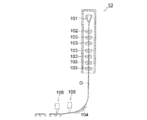
- FIG. 1 It is sectional drawing of the transparent conductive glass substrate which concerns on the 1st Embodiment of this invention. It is a figure which shows an example of the manufacturing method of the glass substrate used for this invention.
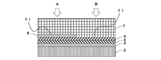
- a patterned resist layer is formed on the transparent conductive glass substrate according to the first embodiment of the present invention, and after removing a part of the transparent conductive layer and removing the resist, the transparent adhesive layer is laminated. It is sectional drawing shown. This is the relationship between the difference in reflectance between the remaining area of the transparent conductive layer and the removed area in the optical film thickness Tc of the transparent conductive layer and the optical film thickness T1 of the first transparent dielectric layer on the front side of the substrate.
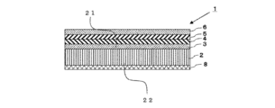
- the transparent conductive glass substrate (1) As shown in FIG. 1, the transparent conductive glass substrate (1) according to the first embodiment of the present invention has an undercoat layer (3) and a first transparent dielectric layer (4) on the glass substrate (2). A second transparent dielectric layer (5) and a transparent conductive layer (6) are formed.
- silicate glass, silica glass, borosilicate glass, soda lime glass, aluminosilicate glass, alkali-free glass, or the like can be used.
- silica glass, borosilicate glass, soda lime glass, and aluminosilicate glass are preferably used, and alkali-free glass is most preferably used.
- non-alkali glass the transparency of the transparent conductive glass substrate (1) can be improved, and when used for a touch panel, the color of the display device is impaired. Can be prevented.
- glass is generally excellent in weather resistance, when an alkali component is contained in the glass substrate (2), cations are dropped on the surface, and so-called soda blowing phenomenon occurs.
- the alkali-free glass is a glass that does not substantially contain an alkali component (alkali metal oxide), and specifically, a glass having a weight ratio of the alkali component of 1000 ppm or less. It is.
- the weight ratio of the alkali component in the present invention is preferably 500 ppm or less, more preferably 300 ppm or less.
- the thickness of the glass substrate (2) is preferably 20 ⁇ m to 200 ⁇ m, most preferably 50 ⁇ m to 100 ⁇ m. Thereby, the thickness of the glass substrate (2) can be further reduced, the transparent conductive glass substrate (1) can be reduced in weight, and by providing flexibility, the glass of the curved surface device (flexible device) can be obtained. It can be used as a substrate. When the thickness of the glass substrate (2) is less than 20 ⁇ m, the strength of the glass substrate (2) tends to be insufficient.
- the glass substrate (2) used in the present invention can be produced by using a known float method, rollout method, slot down draw method, redraw method, etc., but as shown in FIG. It is preferably molded by a draw method. Thereby, a glass substrate (glass film) with a thickness of 300 ⁇ m or less can be produced in large quantities and at low cost.
- the glass substrate (2) produced by the overflow downdraw method does not need to adjust the thickness of the glass substrate (2) by polishing, grinding, chemical etching or the like.
- the overflow downdraw method is a molding method in which both sides of the glass plate do not come into contact with the molded member during molding, and both sides (translucent surface) of the obtained glass plate are fire-making surfaces, so it is not necessary to polish them. High surface quality can be obtained. As a result, when the glass substrate (2) and the first transparent dielectric layer (4) are directly laminated, as described later, the adhesion between the glass substrate (2) and the undercoat layer (3). Both adhesion forces can be improved.
- the molding apparatus (10) is provided with a molded body (101) having a wedge-shaped cross-sectional shape.
- glass molten glass
- a melting furnace not shown
- the molten glass overflows on both sides from the groove formed at the top of the molded body (101).
- the overflowing molten glass flows down along both side surfaces of the molded body (101) and joins at the lower end of the molded body (101).
- molding of a glass film ribbon (G) is started from molten glass.
- the glass ribbon (G) immediately after joining at the lower end of the molded body (101) is drawn downward while being contracted in the width direction by the cooling roller (102), and thinned to a predetermined thickness.
- the glass ribbon (G) thinned to a predetermined thickness is fed by the roller (103), it is gradually cooled by a slow cooling furnace (annealer) to remove the thermal strain of the glass ribbon (G), and the glass film
- the ribbon (G) is sufficiently cooled to a temperature of about room temperature.
- the glass film ribbon (G) that has passed through the slow cooling furnace has its traveling direction changed from the vertical direction to the horizontal direction by the auxiliary roller (104), unnecessary portions existing at both ends in the width direction of the glass film ribbon (G) ( The portion where the cooling roller (102), the roller (103), etc. are in contact) is cut along the longitudinal direction by the cutting device (105).
- the glass film ribbon (G) is cut at predetermined lengths along the width direction by the cutting device (106).
- the glass substrate (2) used by this invention can be obtained.
- the glass substrate (2) cuts the glass film ribbon (G) in the width direction by the cutting device (106), and then the unnecessary portion of the glass film ribbon (G) along the longitudinal direction by the cutting device (105). And may be cut.
- the method for producing a thin-walled flexible glass-like glass substrate (2) has been described, when a relatively thick glass substrate (2) having a thickness of 500 ⁇ m or more is formed, Without providing the auxiliary roller (104), the glass substrate (2) can also be manufactured in a sheet mode by cutting every predetermined length with the cutting device (106).
- the undercoat layer (3) is provided between the glass substrate (2) and the first transparent dielectric layer (4), and the first transparent dielectric layer (4) is laminated on the glass substrate (2). It is a layer to do.
- this underlayer is used.
- the coat layer (3) may not be provided.
- the glass substrate (2) and the first transparent dielectric layer (4) can be brought into close contact with each other, particularly from the viewpoint of barrier properties, transparency, film formation cost, and refractive index. It is preferable to use silicon oxide or tin oxide.
- the first transparent dielectric layer (4) is a layer made of a material having a higher refractive index than the second transparent dielectric layer (5) described later.
- the refractive index of the first transparent dielectric layer (4) is preferably 2.0 to 2.5, and more preferably 2.2 to 2.4.
- the first transparent dielectric layer (4) is not particularly limited as long as it has a higher refractive index than that of the second transparent dielectric layer (5).
- silicon nitride, aluminum nitride, zirconium oxide, One kind selected from niobium oxide, tantalum oxide, hafnium oxide, titanium oxide, tin oxide, zinc oxide, and the like can be used. Of these, niobium oxide is preferably used in terms of transparency, film formation ease, film formation cost, and refractive index.
- the second transparent dielectric layer (5) is a layer made of a material having a refractive index lower than that of the first transparent dielectric layer (4).
- the refractive index of the second transparent dielectric layer (5) is preferably 1.35 to 1.9.
- the second transparent dielectric layer (5) is not particularly limited as long as it has a lower refractive index than that of the first transparent dielectric layer (4).
- silicon oxide, aluminum oxide, and magnesium fluoride are used. 1 type selected from can be used. Among these, it is preferable to use silicon oxide from the viewpoint of transparency, film formation ease, film formation cost, and refractive index.
- FIG. 1 shows a two-layer structure of a first transparent dielectric layer (4) having a high refractive index and a second transparent dielectric layer (5) having a low refractive index, but is not limited thereto.
- a transparent dielectric layer having a low refractive index and a transparent dielectric layer having a high refractive index can be alternately laminated.
- the transparent conductive layer (6) is a layer provided for imparting conductivity to the glass substrate (2) which is a dielectric.
- the refractive index of the transparent conductive layer (6) is preferably 1.7 to 2.3, more preferably 1.9 to 2.1.
- metal thin films such as gold, silver, and aluminum, oxide thin films such as tin-containing indium oxide (ITO), antimony-containing tin oxide, fluorine-containing tin oxide, and aluminum-containing zinc oxide can be used.
- ITO tin-containing indium oxide
- ITO tin-containing indium oxide
- ITO tin-containing indium oxide
- a sputtering method because a dense film can be formed and the wear resistance is excellent.
- these film formation can be performed using the following methods. First, about a glass film ribbon (G) shape
- the film is continuously formed by a so-called roll-to-roll method.
- the transparent conductive glass substrate (1) since the transparent conductive glass substrate (1) is used, it is excellent in heat resistance compared with the case where a transparent resin board is used as a base material. Therefore, in the case where the transparent conductive layer (6) is formed on the glass substrate (2), the film forming step can be performed in a high temperature environment of 150 ° C. or higher, and a film having a low volume resistivity can be formed. it can. This makes it possible to reduce the film thickness of the transparent conductive layer (6) by about 50% compared to the case where the film is formed at room temperature, and the pattern of the transparent conductive layer (6) is more noticeable after patterning. It can be surely prevented.
- FIG. 3 shows the formation of a patterned resist layer on the transparent conductive glass substrate (1) according to the first embodiment of the present invention, and removal of part of the transparent conductive layer (6) and removal of the resist layer. It is sectional drawing which showed the state which laminated
- the transparent conductive glass substrate (1) according to the present invention is used for an electronic device such as a touch panel, a patterned resist layer (not shown) is formed after the transparent conductive layer (6) is formed.
- an etching process for patterning the transparent conductive layer (6) is performed using an etching solution such as hydrochloric acid.
- the peeling process which peels a resist layer from the transparent conductive layer (6) is performed using peeling liquid, such as KOH.
- a transparent adhesive layer (7) as shown in FIG. 3 is laminated.
- the material of the transparent adhesive layer (7) is not particularly limited, and a double-sided pressure-sensitive adhesive sheet, a thermoplastic adhesive sheet, a thermally crosslinkable adhesive sheet, an energy curable liquid adhesive, or the like can be used. Adhere using optical transparent adhesive sheet, EVA, TPU, PVB, ionoplast resin, acrylic thermoplastic adhesive sheet, UV curable adhesive, thermosetting adhesive, room temperature curable adhesive, etc. Also good. When using an adhesive, it is preferable to use an adhesive that can maintain a transparent state after bonding.
- the refractive index of the transparent adhesive layer (7) is preferably 1.4 to 1.6. If the refractive index is a value within this range, the pattern of the transparent conductive layer (6) can be made less noticeable when the transparent conductive glass substrate (1) is used for an electronic device such as a touch panel. Moreover, the design of the first transparent dielectric layer (4) and the second transparent dielectric layer (5) can be facilitated by limiting the refractive index of the transparent adhesive layer (7) to a certain range. it can.
- the transparent conductive layer (6) shown in FIG. 3 is present, and the transparent conductive layer (6) and the transparent adhesive layer (7) form an interface (61).
- the refractive index and thickness of the first transparent dielectric layer (4), the second transparent dielectric layer (5), and the transparent conductive layer (6) are designed so as to be substantially the same.
- the transparent conductive layer (6) can be made inconspicuous.
- FIG. 4 is a diagram showing the relationship of the difference in reflectance, as seen from the substrate front side (transparent adhesive layer (7) side), in regions A and B in FIG.
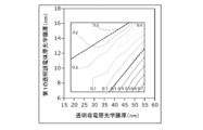
- FIG. 4 shows the transparent conductive in the optical film thickness Tc of the transparent conductive layer (6) and the optical film thickness T1 of the first transparent dielectric layer (4) from the substrate front side (transparent adhesive layer (7) side).
- the reflectance difference between the remaining region (region A in FIG. 3) and the removal region (region B in FIG. 3) of the layer (6) is shown.
- the optical film thickness is a number obtained by multiplying the film thickness of the physical layer by the refractive index of the substance forming the layer.
- the optical film thickness of the first transparent dielectric layer (4) and the optical film thickness of the transparent conductive layer (6) so as to satisfy the above. Thereby, the difference in reflectance between the remaining region (region A in FIG. 3) and the removal region (region B in FIG. 3) of the transparent conductive layer (6) can be reduced to 0.3% or less.
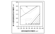
- FIG. 5 shows the relationship in reflectance difference between the regions A and B in FIG. 3 as viewed from the substrate back side (glass substrate (2) side).
- FIG. 5 shows the transparent conductive in the optical film thickness Tc of the transparent conductive layer (6) and the optical film thickness T1 of the first transparent dielectric layer (4), as viewed from the substrate back side (glass substrate (2) side).
- region B of FIG. 3) of a layer (6) is shown.
- the first transparent dielectric layer (4) and the transparent conductive layer (6) so as to satisfy the above. Thereby, the difference in reflectance between the remaining region (region A in FIG. 3) and the removal region (region B in FIG. 3) of the transparent conductive layer (6) can be reduced to 0.3% or less.
- the transparent conductive glass substrate (1) according to the present invention is suitably used for a device such as a touch panel. It is possible, T1 ⁇ 0.2 ⁇ Tc + 7.1 and T1 ⁇ 0.3 ⁇ Tc ⁇ 5.0 If the first transparent dielectric layer (4) and the transparent conductive layer (6) are designed so as to satisfy the above, the transparent conductive glass substrate (1) according to the present invention is more suitably used for a device such as a touch panel. can do.
- FIG. 6 is a diagram showing the optimum values of the optical film thickness of the transparent conductive layer (6) and the optical film thickness of the second transparent dielectric layer (5). Applying the relationships shown in FIGS. 4, 5, and 6, the refractive index and film thickness of the first transparent dielectric layer (4), and the refractive index and film thickness of the second transparent dielectric layer (5). It is preferable to determine the refractive index and film thickness of the transparent conductive layer (6).
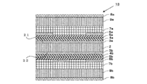
- the transparent conductive glass substrate (1) As shown in FIG. 7, the transparent conductive glass substrate (1) according to the second embodiment of the present invention has an undercoat layer (3a) on one surface (21) of the glass substrate (2), A transparent dielectric layer (4a), a second transparent dielectric layer (5a), and a transparent conductive layer (6a) are formed, an undercoat layer (3b) on the other surface (21), and a first A transparent dielectric layer (4b), a second transparent dielectric layer (5b), and a transparent conductive layer (6b) are formed.
- Undercoat layers (3a) and (3b), first transparent dielectric layers (4a) and (4b), second transparent dielectric layers (5a) and (5b), and a transparent conductive layer (6a) , (6b) is the same as that of the first embodiment described above, except for the matters described below.
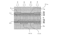
- FIG. 8 shows the formation of a patterned resist layer on the transparent conductive glass substrate (1) according to the second embodiment of the present invention, and removal of part of the transparent conductive layers (6a) and (6b). It is sectional drawing which showed the state which laminated
- the patterning method of the transparent conductive layers (6a) and (6b) and the configuration of the transparent adhesive layers (7a) and (7b) are the same as those in the first embodiment described above.
- Region C The transparent conductive layer (6a) and the transparent adhesive layer (7a) form an interface (61a) on one surface (21) side, and the second transparent dielectric is formed on the other surface (22) side.
- Region D second transparent dielectric layer (5a) on one surface (21) side and transparent adhesive layer (7a) ) And forming the interface (51a) on the other surface (22) side, and forming the interface (61b) with the transparent conductive layer (6b) and the transparent adhesive layer (7b).
- Region E One surface On the (21) side, the second transparent dielectric layer (5a) and the transparent adhesive layer (7a) form an interface (51a), and on the other side (22) side, the second transparent dielectric layer ( 5b) and a region where an interface (51b) is formed by the transparent adhesive layer (7b)
- Region F a transparent conductive layer (6a) on one surface (21) side And the transparent adhesive layer (7a) form an interface (61a), and the other surface (22) side forms an interface (61b) between the transparent conductive layer (6b) and the transparent adhesive layer (7b).
- Region The first transparent dielectric layers (4a) and (4b), the second transparent dielectric layers (5a) and (5b), and the transparent conductive layer so that the reflectances of these four regions are substantially the same.
- the refractive index and thickness of (6a) and (6b) are designed. Thereby, in the state of the transparent conductive glass substrate (1) before bonding, even if the pattern of the transparent conductive layer (6) is slightly conspicuous, the transparent conductive glass substrate (1) is actually attached to the transparent adhesive layer.
- the pattern of the transparent conductive layer (6) can be made inconspicuous. Specifically, it is necessary to reduce the difference in reflectance between the region C, the region D, the region E, and the region F having different conditions, and is the surface reflectance on both surfaces (front and back surfaces) of the glass substrate (2).
- the pattern of the transparent conductive layer (6) becomes inconspicuous when the reflectance difference is 2% or less, which is half of 8%, that is, one side.
- the reflectance difference between the two surfaces (front and back surfaces) of the glass substrate (2) is 0.6% or less, that is, by making the reflectance difference for one surface 0.3% or less, a transparent conductive layer ( The pattern of 6) becomes inconspicuous.
- the optical film thickness Tc of the transparent conductive layer (6a) and the optical film thickness T1 of the first transparent dielectric layer (4a) are similar to the equation derived from FIG.
- the optical film thickness of the first transparent dielectric layer (4a) and the optical film thickness of the transparent conductive layer (6a) are similar to the formulas derived from FIG. T1 ⁇ 0.2 ⁇ Tc + 7.1 and T1 ⁇ 0.3 ⁇ Tc ⁇ 5.0 It is preferable to design the optical film thickness of the first transparent dielectric layer (4b) and the optical film thickness of the transparent conductive layer (6b) so as to satisfy the above.
- the optical film thickness Tc of the transparent conductive layer (6b) and the optical film thickness T1 of the first transparent dielectric layer (4b) are Even if T1 ⁇ 0.2 ⁇ Tc + 7.9 and T1 ⁇ 0.3 ⁇ Tc ⁇ 5.3 are satisfied, substantially equivalent characteristics can be obtained.
- the transparent conductive glass substrate (1) As shown in FIG. 9, the transparent conductive glass substrate (1) according to the third embodiment of the present invention has an undercoat layer (3) and a first surface on one surface (21) of the glass substrate (2).
- the transparent dielectric layer (4), the second transparent dielectric layer (5), and the transparent conductive layer (6) are formed, and an antireflection film layer (8) having a multilayer structure is formed on the other surface (22). ) Is formed.
- the luminous reflectance of the antireflection film layer (8) is preferably 0.5% or less. Thereby, reflection can be prevented and an electronic device such as a touch panel with good visibility can be manufactured.
- the configurations of the undercoat layer (3), the first transparent dielectric layer (4), the second transparent dielectric layer (5), and the transparent conductive layer (6) are the same as in the first embodiment.
- the antireflection film layer (8) is preferably made of an inorganic material, and is preferably made of a film in which low refractive index layers and high refractive index layers are alternately stacked.
- the number of layers in which the low refractive index layer and the high refractive index layer are alternately stacked is preferably 4 to 20 layers.
- the low refractive index layer is preferably one kind selected from the group consisting of silicon oxide, aluminum oxide and magnesium fluoride, and the total physical film thickness of the low refractive index layer on one side is preferably 100 nm to 700 nm.
- the high refractive index layer is preferably one kind selected from the group consisting of silicon nitride, aluminum nitride, zirconium oxide, niobium oxide, tantalum oxide, hafnium oxide, titanium oxide, tin oxide and zinc oxide.
- the total physical film thickness of the high refractive index layer is preferably 50 nm to 400 nm.
- the antireflection film layer (8) on the glass substrate (2) methods such as sputtering, vacuum deposition, dipping, spin coating, ion plating, and CVD can be used.
- a sputtering method because the film thickness is uniform, the adhesion to the glass substrate (2) is strong, and the film hardness is increased.
- the transparent conductive glass substrate (1) according to the first embodiment is passed through the transparent adhesive layer (7) after patterning of the transparent conductive layer (6).
- the electronic device touch panel (13) is produced.
- an alkali-free glass (product name: OA-10G, thermal expansion coefficient at 30 to 380 ° C .: 38 ⁇ 10 ⁇ 7 / ° C.) having a thickness of 50 ⁇ m manufactured by Nippon Electric Glass Co., Ltd. was prepared.
- an undercoat layer (3) composed of silicon oxide (SiO 2 ) and a first layer composed of niobium oxide (Nb 2 O 5 ) are formed from the lower layer.
- the transparent dielectric layer (4), the second transparent dielectric layer (5) made of silicon oxide (SiO 2 ), and the transparent conductive layer (6) made of ITO are laminated in this order, so that the transparent conductive layer shown in FIG. Glass substrate (1) was produced. From the relationship shown in FIG. 4, FIG. 5, and FIG. 6, when the transparent adhesive layer (7) is laminated, the difference in reflectance depending on the presence or absence of the transparent conductive layer (6) is 0.01%.
- the optical film thickness of the undercoat layer (3) of the transparent conductive glass substrate (11) viewed from the front is 15 nm
- the optical film thickness of the first transparent dielectric layer (4) is 10 nm
- the second transparent dielectric layer The optical film thickness of 5
- the transparent conductive glass substrate (12) viewed from the rear side of the substrate is 0.01% so that the difference in reflectance depending on the presence or absence of the transparent conductive layer (6) is 0.01%.
- the optical film thickness of the undercoat layer (3) is 15 nm
- the optical film thickness of the first transparent dielectric layer (4) is 9 nm
- the optical film thickness of the second transparent dielectric layer (5) is 82 nm
- the optical film thickness of (6) was 33 nm.
- a patterned resist layer was formed on the surfaces of the transparent conductive glass substrate (11) viewed from the front of the substrate and the transparent conductive layer (6) of the transparent conductive glass substrate (12) viewed from the back of the substrate. Thereafter, the transparent conductive layer (6) was etched with hydrochloric acid. Thereafter, the resist layer was removed with KOH.
- a transparent adhesive layer (7) is formed on the surface of the transparent conductive layer (6), and the transparent conductive glass substrate (11) viewed from the front of the substrate and the transparent conductive glass substrate (12) viewed from the back of the substrate are transparent.
- the touch panel (13) shown in FIG. 10 was produced by bonding the conductive layers (6) so as to face each other. When the produced touch panel (13) was observed from the transparent conductive glass substrate (12) side viewed from the back of the substrate (from the top of FIG. 10), the pattern of the transparent conductive layer (6) was not conspicuous. Moreover, when the reflectance was measured, the difference between the maximum reflectance and the minimum reflectance was 0.02%.
- the fifth embodiment of the present invention is transparent on both outer surfaces after patterning the transparent conductive layers (6a) and (6b) of the transparent conductive glass substrate (1) according to the second embodiment. After laminating the adhesive layers (7a) and (7b), the glass sheets (9a) and (9b) are bonded to produce an electronic device (touch panel (13)).
- an alkali-free glass (product name: OA-10G, thermal expansion coefficient at 30 to 380 ° C .: 38 ⁇ 10 ⁇ 7 / ° C.) having a thickness of 50 ⁇ m manufactured by Nippon Electric Glass Co., Ltd. was prepared.
- an undercoat layer (3a) made of silicon oxide (SiO 2 ) and niobium oxide (Nb 2 O 5 ) are formed from the glass substrate (2) side.
- a first transparent dielectric layer (4a) made of, a second transparent dielectric layer (5a) made of silicon oxide (SiO 2 ), and a transparent conductive layer (6a) made of ITO were laminated.
- the optical film thickness of the undercoat layer (3a) on the one surface (21) side of the transparent conductive glass substrate (1) is 15 nm
- the optical film thickness of the first transparent dielectric layer (4a) is 10 nm
- the optical film thickness of the second transparent dielectric layer (5a) was 78 nm
- the optical film thickness of the transparent conductive layer (6) was 33 nm.
- the other surface (1) of the transparent conductive glass substrate (1) is set so that the difference in reflectance depending on the presence or absence of the transparent conductive layer (6) is 0.01% 22)
- the optical thickness of the undercoat layer (3) on the side is 15 nm
- the optical thickness of the first transparent dielectric layer (4) is 9 nm
- the optical thickness of the second transparent dielectric layer (5) is 82 nm.
- the optical film thickness of the transparent conductive layer (6) was 33 nm.
- a patterned resist layer was formed on the surface of the transparent conductive layers (6a) and (6b) of the transparent conductive glass substrate (1). Thereafter, the transparent conductive layers (6a) and (6b) were etched with hydrochloric acid.
- the remaining part of the resist layer was removed by KOH. Thereafter, the transparent adhesive layers (7a) and (7b) are formed on the surfaces of the transparent conductive layers (6a) and (6b), and the glass sheets (9a) and (9b) having a thickness of 100 ⁇ m are adhered to each other.
- a touch panel (13) shown in FIG. When the produced touch panel (13) was observed from one surface (21) side of the glass substrate (2) (from the upper part of FIG. 11), the pattern of the transparent conductive layers (6a) and (6b) was not conspicuous. . When the reflectance was measured, the difference between the maximum reflectance and the minimum reflectance was 0.02%.
- the sixth embodiment according to the present invention has a transparent conductive glass substrate (1) according to the third embodiment and a transparent adhesive layer (7) after patterning of the transparent conductive layer (6).
- the electronic device touch panel (13)
- This touch panel (13) is the same as the touch panel described in the fourth embodiment except that the antireflection film layer (8) is formed on the other surface (22) of the glass substrate (2). It is a configuration.
- the antireflection film layer (8) is a film in which five layers of a low refractive index layer made of SiO 2 and a high refractive index layer made of Nb 2 O 5 are alternately stacked. A high refractive index layer made of Nb 2 O 5 is formed on the glass substrate (2) side, and a low refractive index layer made of SiO 2 is formed on the outermost layer.
- an antireflection film layer (8a) is further added to the outermost layer of the glass sheets (9a) and (9b).
- (8b) is a touch panel (13).
- the configurations of the antireflection film layers (8a) and (8b) are the same as those of the touch panel according to the sixth embodiment described above, and other configurations are the same as those of the touch panel according to the fifth embodiment described above. It is similar to the one.
- a transparent adhesive layer (7) is laminated on the outer side of the touch panel according to the fifth embodiment described above, and an antireflection film layer (8) is provided. It is the touch panel which laminated
- the configuration of the glass sheet (9) is the same as that of the touch panel according to the fifth embodiment described above.
- the configuration of the antireflection film layer (8) is the same as that of the touch panel according to the sixth embodiment described above.
- the present invention can be suitably used for a touch panel used in a mobile phone, a smartphone, a tablet type, or a notebook type PC.
Landscapes
- Engineering & Computer Science (AREA)
- Chemical & Material Sciences (AREA)
- Life Sciences & Earth Sciences (AREA)
- Chemical Kinetics & Catalysis (AREA)
- General Chemical & Material Sciences (AREA)
- Geochemistry & Mineralogy (AREA)
- Materials Engineering (AREA)
- Organic Chemistry (AREA)
- General Engineering & Computer Science (AREA)
- Theoretical Computer Science (AREA)
- Human Computer Interaction (AREA)
- Physics & Mathematics (AREA)
- General Physics & Mathematics (AREA)
- Laminated Bodies (AREA)
- Position Input By Displaying (AREA)
- Non-Insulated Conductors (AREA)
- Physical Vapour Deposition (AREA)
Description
本発明は、携帯電話、スマートフォン、タブレット型やノート型のPC、銀行のATMや券売機等に用いられるタッチパネルと、当該タッチパネル等の電子デバイスに用いられる透明導電性ガラス基板に関する。
銀行のATMやゲームセンターのゲーム、鉄道やバス等の券売機に、従来からタッチパネルが使用されている。タッチパネルが搭載された表示装置は、表示された情報から視覚を通じて直感的に機器の操作を行うことが可能となるため、装置の操作が容易になるという利点を有する。
また、タッチパネルが搭載された表示装置には、別途入力装置を設ける必要がなく、装置全体の小型化が可能になる。従って、小型化が要求される携帯電話やスマートフォン、携帯型ゲーム機器、タブレット型PCやノート型PCに、近年、タッチパネルが好適に使用されている。
タッチパネルは、使用用途に合わせて、抵抗膜方式、表面弾性波方式、赤外線方式、電磁誘導方式、静電容量方式等、種々の方式が採用されるが、タッチパネル上の複数箇所に指が同時に触れた場合に、各々の接触位置の正確な検出を可能とするために、近年、静電容量方式のタッチパネルが、スマートフォンやタブレット型PC等に採用されている。
静電容量方式のタッチパネルでは、透明誘電体の両側に縦横2層からなる透明導電層が設けられているため、導体である指がタッチパネルに接触した際に、接触位置における電極の静電容量の変化を縦横2つの電極列から知ることができ、接触位置を精密に判別できるようになっている。このように接触位置を正確に判別するために、静電容量方式のタッチパネルでは、ガラス基板等の透明誘電体の全面に、透明導電層としての透明導電膜を精密に形成(パターンニング)する必要がある。ここで、この透明導電膜は、線状(縦横では格子状)に形成されるため、ガラス基板等の透明誘電体上には、透明導電膜が形成された領域と、透明導電膜が形成されていない領域とが存在することになる。そして、透明導電膜は、文字通りの透明であるため、一般的には、透明導電膜の形成パターンを視認できないものとされている。
しかしながら、透明導電膜は、透明であるとはいっても、ガラス基板上における透明導電膜の有無によって反射率が異なるため、見方によっては透明導電膜のパターンの形状が目立ってしまい、タッチパネルスクリーンの視認性が悪化し、美観を損なうという問題があった。
この問題を解決するために、特許文献1には、透明基板と透明導電膜の間に、透明導電膜が形成された領域の反射率と、透明導電膜が形成されていない領域の反射率とを近似させるための調節層を設けることが提案されている。これにより、透明基板上に形成された透明導電膜の有無による反射率の違いがある程度抑えられることとなり、タッチパネルの視認性が、ある程度向上している。
しかしながら、特許文献1に記載の方法を採用した場合、タッチパネル製造前の透明基板単体の状態では、透明導電膜のパターンを認識し難く、透明導電膜のパターンが目立たなかったにも関わらず、この透明基板を使用して製造されたタッチパネルにおいては、透明導電膜のパターンが僅かに目立ってくるという問題が生じていた。
本発明は、上述のような従来技術の問題点を解決するためになされたものであって、透明基板を使用してタッチパネルを製造した場合に、透明導電膜のパターンが目立つことが無く視認性が向上する透明基板及びタッチパネルを提案することを目的とする。
発明者らは鋭意研究の結果、以下のことを知見し本発明へと至った。すなわち、透明基板単体の状態で、透明導電層が形成された領域の反射率と、透明導電層が形成されていない領域の反射率との違いが低減されていたとしても、透明基板は屈折率1.0である大気と界面を形成しており、実際にタッチパネルを製造する場合においては、屈折率1.4~1.6の透明接着層を介してタッチパネルを製造することとなる。これに起因して、その界面である大気中と透明接着層との屈折率の差が原因となり、透明基板単体の状態では透明導電層のパターンが目立たなかったとしても、この透明基板を使用して製造されたタッチパネルにおいては、透明導電層のパターンが僅かに目立ってくるということを知見した。
上記目的を達成するために創案された本発明は、ガラス基板と、該ガラス基板の一方の面に形成された少なくとも2層の透明誘電体層と、該透明誘電体層の表面に形成された透明導電層とを含む透明導電性ガラス基板であって、前記透明導電層の一部が除去されて前記透明誘電体層の一部が露出した露出部、及び前記透明導電層の表面に透明接着層を積層した場合に、前記透明誘電体層の露出部と前記透明接着層との界面での反射率と、前記透明導電層と前記透明接着層との界面での反射率とが、略同一となることに特徴付けられる。ここで、「透明誘電体層の露出部と透明接着層との界面での反射率と、透明導電層と透明接着層との界面での反射率とが、略同一」とは、具体的には、透明誘電体層の露出部と透明接着層との界面での反射率と、透明導電層と透明接着層との界面での反射率との差が2%以下であることを意味する。「2%以下」とは、透明誘電体層の露出部と透明接着層との界面での反射率の値を基準とした2%以下と、透明導電層と透明接着層との界面での反射率の値を基準とした2%以下とのいずれであってもよいことを意味する。なお、反射率の差としては、0.3%以下であることがより好ましい。また、「反射率」とは、波長550nmでの値を意味する。
上記の透明導電性ガラス基板において、前記透明誘電体層は、前記ガラス基板の一方の面に積層された第1透明誘電体層と、該第1透明誘電体層の表面に積層された第2透明誘電体層からなる2層構造を有し、
前記第1の透明誘電体層の物理膜厚と屈折率との積を光学膜厚T1とし、
前記透明導電層の物理膜厚と屈折率との積を光学膜厚Tcとした場合に、
T1≦0.2×Tc+7.9 且つ、
T1≧0.3×Tc-5.3
を満たすことが好ましい。ここで、「屈折率」とは、波長550nmでの値を意味する。
前記第1の透明誘電体層の物理膜厚と屈折率との積を光学膜厚T1とし、
前記透明導電層の物理膜厚と屈折率との積を光学膜厚Tcとした場合に、
T1≦0.2×Tc+7.9 且つ、
T1≧0.3×Tc-5.3
を満たすことが好ましい。ここで、「屈折率」とは、波長550nmでの値を意味する。
上記の透明導電性ガラス基板において、前記ガラス基板と前記透明誘電体層の間には、アンダーコート層が形成されていることが好ましい。
上記の透明導電性ガラス基板において、前記透明接着層の屈折率は、1.4~1.6であることが好ましい。
上記の透明導電性ガラス基板において、前記ガラス基板の板厚は、20~200μmであることが好ましい。
上記の透明導電性ガラス基板において、前記ガラス基板は、無アルカリガラスであることが好ましい。
上記の透明導電性ガラス基板において、前記ガラス基板の他方の面に反射防止膜層が形成されていることが好ましい。
上記の透明導電性ガラス基板において、前記ガラス基板の他方の面に、前記透明誘電体層と、前記透明導電層が形成されていることが好ましい。
上記の透明導電性ガラス基板において、前記ガラス基板の他方の面に、前記アンダーコート層と、前記透明誘電体層と、前記透明導電層が形成されていることが好ましい。
また、上記の透明導電性ガラス基板の2枚を、前記透明導電層側が対向するように配置し、前記透明接着層を介して接着することで、上記の目的を達成することが可能なタッチパネルとすることができる。
さらに、上記の透明導電性ガラス基板の両面に、前記透明接着層を介してガラスシートを接着したタッチパネルにおいても、上記の目的を達成することができる。
上記のタッチパネルにおいて、少なくとも1枚の前記ガラスシートの前記透明接着層との非接着面側には、反射防止膜層が形成されていることが好ましい。
本発明によれば、タッチパネル等の電子デバイスを作製する際、透明導電性ガラス基板の透明導電層のパターン処理後に、透明誘電体層の露出部、及び透明導電層の表面に透明接着層を積層した場合に、透明誘電体層の露出部と透明接着層との界面での反射率と、透明導電層と透明接着層との界面での反射率とが、略同一となる。そのため、この透明導電性ガラス基板を、透明接着層を介してタッチパネル等の電子デバイスに組み込んだとしても、透明導電層のパターンが目立つことが無く、表示装置の表示性能を向上させることが可能となる。言い換えれば、接着前の透明導電性ガラス基板単体の状態では、透明導電層のパターンが僅かに目立っていたとしても、実際に透明接着層を介してタッチパネル等の電子デバイスに組み込んだ場合に、透明導電層のパターンを目立たなくすることができる。また、透明基板としてガラス基板を使用することで、透明導電層の厚みを薄くすることができ、透明導電層のパターンを目立たなくすることができる。
本発明のある実施態様によれば、ガラス基板の一方の面に積層された第1の透明誘電体層の物理膜厚と屈折率との積を光学膜厚T1とし、透明導電層の物理膜厚と屈折率との積を光学膜厚Tcとした場合に、
T1≦0.2×Tc+7.9 且つ、
T1≧0.3×Tc-5.3
を満たすから、透明誘電体層の露出部、及び透明導電体層の表面に透明接着層を積層した場合に、透明誘電体層の露出部と透明接着層との界面での反射率と、透明導電層と透明接着層との界面での反射率との差を0.3%以下とすることができる。これにより、透明接着層を介して透明導電性ガラス基板をタッチパネル等の電子デバイスに組み込んだ場合に、透明導電層のパターンをより確実に目立たなくすることができる。
T1≦0.2×Tc+7.9 且つ、
T1≧0.3×Tc-5.3
を満たすから、透明誘電体層の露出部、及び透明導電体層の表面に透明接着層を積層した場合に、透明誘電体層の露出部と透明接着層との界面での反射率と、透明導電層と透明接着層との界面での反射率との差を0.3%以下とすることができる。これにより、透明接着層を介して透明導電性ガラス基板をタッチパネル等の電子デバイスに組み込んだ場合に、透明導電層のパターンをより確実に目立たなくすることができる。
本発明のある実施態様によれば、ガラス基板と透明誘電体層の間には、アンダーコート層が形成されていることから、より確実に、ガラス基板上に第1の透明誘電体層を積層することができる。
本発明のある実施態様によれば、透明接着層の屈折率は、1.4~1.6であることから、実際にタッチパネル等の電子デバイスを作製する際に、電子デバイス作製前には僅かに透明導電層のパターンが目立っていたとしても、透明接着層を介して透明導電性ガラス基板をタッチパネル等の電子デバイスに組み込んだ場合に、透明導電層のパターンをより確実に目立たなくすることができる。また、透明接着層の屈折率は、1.4~1.6と規定することで、透明誘電体層の露出部と透明接着層との界面での反射率と、透明導電体層と透明接着層との界面での反射率とが、設計値から乖離することを防止することができる。
本発明のある実施態様によれば、ガラス基板の板厚は、20~200μmであって、可撓性を有するため、曲面を有するタッチパネル等のデバイスへの適用が可能となる。
本発明のある実施態様によれば、ガラス基板は、無アルカリガラスであることから、ガラス基板の透明性が一般的なソーダガラスよりも向上する。そのため、タッチパネル等の表示装置に組み込んだ場合に、当該表示装置の視認性を向上させることができる。
本発明のある実施態様によれば、ガラス基板の他方の面に反射防止膜層が形成され、反射防止膜の視感反射率が0.5%以下であることから、映り込みを防止し、より確実に表示装置の視認性を向上させることができる。表面に反射防止処理を施した場合については、透明導電層のパターンがより目立つ傾向にあるが、本発明に係る透明導電性ガラス基板を使用することで、タッチパネル等の電子デバイスに組み込んだ際に、透明導電層のパターンを目立たなくすることができる。また、透明樹脂体は耐熱性が低く、表面にスパッタ処理等による反射防止膜の成膜を行うことが困難であるが、ガラス基板は耐熱性に優れるため、容易に反射防止膜を形成することができる。
以下、本発明に係る透明導電性ガラス基板およびタッチパネルの好適な実施形態について、図面を参照して説明する。
(第1の実施形態)
本発明の第1の実施形態に係る透明導電性ガラス基板(1)は、図1に示す通り、ガラス基板(2)上にアンダーコート層(3)、第1の透明誘電体層(4)、第2の透明誘電体層(5)及び透明導電層(6)が形成されている。
本発明の第1の実施形態に係る透明導電性ガラス基板(1)は、図1に示す通り、ガラス基板(2)上にアンダーコート層(3)、第1の透明誘電体層(4)、第2の透明誘電体層(5)及び透明導電層(6)が形成されている。
ガラス基板(2)としては、ケイ酸塩ガラス、シリカガラス、ホウ珪酸ガラス、ソーダライムガラス、アルミノ珪酸塩ガラス、無アルカリガラス等を使用することができる。これらのうち、シリカガラス、ホウ珪酸ガラス、ソーダライムガラス、アルミノ珪酸塩ガラスを使用することが好ましく、無アルカリガラスを使用することが最も好ましい。ガラス基板(2)として無アルカリガラスを使用することで、透明導電性ガラス基板(1)の透明性を向上させることができ、タッチパネルに使用した場合に、表示装置の色味が損なわれるのを防止することができる。また、ガラスは一般的に耐候性に優れるが、ガラス基板(2)にアルカリ成分が含有されている場合には、表面において陽イオンが脱落し、いわゆるソーダ吹きの現象が生じる。これにより、ガラスが構造的に粗となる場合があり、ガラス基板(2)の透光性が悪化するおそれがある。加えて、ガラス基板(2)をフィルム化(薄肉化)することで可撓性を付与し、湾曲させて使用していると、経年劣化により粗となった部分から破損する可能性がある。尚、ここで無アルカリガラスとは、アルカリ成分(アルカリ金属酸化物)が実質的に含まれていないガラスのことであって、具体的には、アルカリ成分の重量比が1000ppm以下のガラスのことである。本発明でのアルカリ成分の重量比は、好ましくは500ppm以下であり、より好ましくは300ppm以下である。
ガラス基板(2)の厚みは、20μm~200μmが好ましく、50μm~100μmが最も好ましい。これによりガラス基板(2)の厚みをより薄くして、透明導電性ガラス基板(1)の軽量化を行うことができると共に、可撓性を付与することで、曲面デバイス(フレキシブルデバイス)のガラス基板として使用することができる。ガラス基板(2)の厚みが20μm未満であると、ガラス基板(2)の強度が不足がちになるおそれがある。
本発明に使用されるガラス基板(2)は、公知のフロート法、ロールアウト法、スロットダウンドロー法、リドロー法等を使用することで製造することができるが、図2に示す通り、オーバーフローダウンドロー法によって成形されていることが好ましい。これにより、厚み300μm以下のガラス基板(ガラスフィルム)を大量かつ安価に作製することができる。オーバーフローダウンドロー法により作製されたガラス基板(2)は、研磨や研削、ケミカルエッチング等によってガラス基板(2)の厚みの調整を行う必要がない。また、オーバーフローダウンドロー法は、成形時にガラス板の両面が、成形部材と接触しない成形法であり、得られたガラス板の両面(透光面)は火づくり面となるため、研磨しなくとも高い表面品質を得ることができる。これにより、ガラス基板(2)とアンダーコート層(3)との密着力や、後述するように、ガラス基板(2)と第1の透明誘電体層(4)とを直接に積層する場合の両者の密着力を向上させることができる。
成形装置(10)には、楔状の断面形状を有する成形体(101)が備えられており、図示省略の溶融窯で溶融されたガラス(溶融ガラス)を成形体(101)に供給することで、当該溶融ガラスが成形体(101)の頂部に形成された溝から両側に溢れ出るようになっている。そして、溢れ出た溶融ガラスは、成形体(101)の両側面を伝って流下し、成形体(101)の下端で合流する。これにより、溶融ガラスからガラスフィルムリボン(G)の成形が開始される。成形体(101)の下端で合流した直後のガラスリボン(G)は、冷却ローラ(102)によって幅方向の収縮が規制されながら下方へ引き伸ばされて所定の厚みまで薄くなる。次に、所定厚みに薄肉化されたガラスリボン(G)をローラ(103)で送りだしながら、徐冷炉(アニーラ)で徐々に冷却して、ガラスリボン(G)の熱歪を除去すると共に、ガラスフィルムリボン(G)を室温程度の温度にまで十分に冷却する。徐冷炉を通過したガラスフィルムリボン(G)は、補助ローラ(104)によって鉛直方向から水平方向へと進行方向を変えた後、ガラスフィルムリボン(G)の幅方向の両端部に存在する不要部分(冷却ローラ(102)やローラ(103)等が接触した部分)を、長手方向に沿って切断装置(105)により切断される。その後、切断装置(106)により、幅方向に沿って所定の長さ毎にガラスフィルムリボン(G)が切断される。これにより、本発明で使用されるガラス基板(2)を得ることができる。なお、ガラス基板(2)は、切断装置(106)によりガラスフィルムリボン(G)を幅方向に切断した後で、切断装置(105)によりガラスフィルムリボン(G)の不要部分を長手方向に沿って切断して作製してもよい。なお、ここまでは、薄肉の可撓性を有するフィルム状のガラス基板(2)を製造する方法について説明したが、比較的厚みのある500μm以上のガラス基板(2)を成形する場合には、補助ローラ(104)を設けずに、切断装置(106)で所定の長さ毎に切断することで、枚様式でガラス基板(2)を製造することもできる。
アンダーコート層(3)は、ガラス基板(2)と第1の透明誘電体層(4)との間に設けられ、ガラス基板(2)上に第1の透明誘電体層(4)を積層するための層である。ここで、第1の透明誘電体層(4)を適宜選択することにより、ガラス基板(2)上に直接第1の透明誘電体層(4)を積層することができる場合については、このアンダーコート層(3)は設けなくともよい。
アンダーコート層(3)としては、ガラス基板(2)と第1の透明誘電体層(4)とを密着させることができ、バリア性、透明性、成膜コスト、屈折率の関係から、特に酸化ケイ素、酸化スズを使用することが好ましい。
第1の透明誘電体層(4)は、後述する第2の透明誘電体層(5)よりも屈折率の高い物質で構成された層である。第1の透明誘電体層(4)の屈折率は、2.0~2.5であることが好ましく、2.2~2.4であることがより好ましい。第1の透明誘電体層(4)としては、第2の透明誘電体層(5)よりも屈折率が高い物質であれば、特に限定されず、例えば、窒化ケイ素、窒化アルミニウム、酸化ジルコニウム、酸化ニオブ、酸化タンタル、酸化ハフニウム、酸化チタン、酸化スズ及び酸化亜鉛等から選択される1種を使用することができる。中でも、透明性、成膜の容易性、成膜コスト、屈折率の関係から、酸化ニオブを使用することが好ましい。
第2の透明誘電体層(5)は、第1の透明誘電体層(4)よりも屈折率の低い物質で構成された層である。第2の透明誘電体層(5)の屈折率は、1.35~1.9であることが好ましい。第2の透明誘電体層(5)としては、第1の透明誘電体層(4)よりも屈折率が低い物質であれば、特に限定されず、例えば、酸化ケイ素、酸化アルミニウム及びフッ化マグネシウムから選択される1種を使用することができる。中でも、透明性、成膜の容易性、成膜コスト、屈折率の関係から、酸化ケイ素を使用することが好ましい。
図1では、屈折率の高い第1の透明誘電体層(4)と屈折率の低い第2の透明誘電体層(5)の2層構造を呈しているが、これには限定されず、屈折率の低い透明誘電体層と屈折率の高い透明誘電体層を、さらに交互に積層することもできる。
透明導電層(6)は、誘電体であるガラス基板(2)に導電性を付与するために設けられる層である。透明導電層(6)の屈折率は、1.7~2.3であることが好ましく、1.9~2.1であることがより好ましい。透明導電層(6)は、金、銀、アルミニウム等の金属薄膜、スズ含有酸化インジウム(ITO)、アンチモン含有酸化スズ、フッ素含有酸化スズ、アルミニウム含有酸化亜鉛等の酸化物薄膜が使用可能であり、特にスズ含有酸化インジウム(ITO)は、成膜が比較的容易であるとともに、可視光線の透過率を高くできるため好ましい。
アンダーコート層(3)、第1の透明誘電体層(4)、第2の透明誘電体層(5)、透明導電層(6)は、イオンプレーティング法、スパッタ法、真空蒸着法等を用いて成膜することできるが、特に、スパッタ法を用いると、緻密な膜が形成でき、耐摩耗性に優れるため好ましい。また、これらの成膜は、以下のような方式を利用して行うことができる。まず、上述のオーバーフローダウンドロー法によって成形されたガラスフィルムリボン(G)について、上記の切断装置(105)により長手方向に沿って不要部分を切断する。そして、不要部分が切断されたガラスフィルムリボン(G)を合紙と重ね合わせた状態でロール状に巻き取り、ガラスロールを作製する。その後、いわゆるロール・ツー・ロール方式で連続的に成膜を行う。また、本発明では、透明導電性ガラス基板(1)を使用しているため、基材として透明樹脂板を使用する場合と比較して、耐熱性に優れる。そのため、ガラス基板(2)上に透明導電層(6)を成膜する場合において、150℃以上の高温環境下で成膜工程を行うことができ、体積抵抗率の低い膜を形成することができる。これにより、常温で成膜した場合と比較して、透明導電層(6)の膜厚を約50%薄くすることが可能となり、パターニング後に、透明導電層(6)のパターンが目立つことをより確実に防止することができる。
図3は、本発明の第1の実施形態に係る透明導電性ガラス基板(1)にパターン化されたレジスト層を形成し、透明導電層(6)の一部の除去及びレジスト層の除去を行った後に、透明接着層(7)を積層した状態を示した断面図である。
本発明に係る透明導電性ガラス基板(1)は、タッチパネル等の電子デバイス等に使用するため、透明導電層(6)の成膜後に、パターニングされた図示省略のレジスト層を形成する。次に、塩酸等のエッチング液を用いて、透明導電層(6)をパターニングするエッチング工程を行う。次に、KOH等の剥離液を用いて、透明導電層(6)の上からレジスト層を剥離する剥離工程を行う。
透明導電層(6)のパターニング後に、図3に示すような透明接着層(7)を積層する。透明接着層(7)の材質については、特には限定されず、両面粘着シート、熱可塑性接着シート、熱架橋性接着シート、エネルギー硬化性の液体接着剤等を使用することができる。また、光学透明粘着シート、EVA、TPU、PVB、アイオノプラスト樹脂、アクリル系熱可塑性接着シート、紫外線硬化型接着剤、熱硬化型接着剤、常温硬化型接着剤等を使用して接着してもよい。接着剤を使用する場合は、接着後に透明状態を維持できる接着剤を使用することが好ましい。
透明接着層(7)の屈折率は、1.4~1.6であることが好ましい。屈折率をこの範囲内の値とすれば、透明導電性ガラス基板(1)をタッチパネル等の電子デバイスに使用した場合に、透明導電層(6)のパターンをより目立たなくすることができる。また、透明接着層(7)の屈折率を一定の範囲に制限することで、第1の透明誘電体層(4)と第2の透明誘電体層(5)の設計を容易にすることができる。
本発明の透明導電性ガラス基板(1)においては、図3に示す透明導電層(6)が存在し、透明導電層(6)と透明接着層(7)とで界面(61)を形成する領域Aの反射率と、透明導電層(6)が存在せず、第2の透明誘電体層(5)と透明接着層(7)とで界面(51)を形成する領域Bの反射率とが、略同一となるように、第1の透明誘電体層(4)、第2の透明誘電体層(5)、及び透明導電層(6)の屈折率と厚みを設計する。これにより、接着前の透明導電性ガラス基板(1)の状態では、透明導電層(6)のパターンが僅かに目立っていたとしても、この透明導電性ガラス基板(1)を、透明接着層(7)を介してタッチパネル等の電子デバイスに組み込んだ場合には、透明導電層(6)のパターンを目立たなくすることができる。
図4は、図3における領域Aと領域Bの、基板正面側(透明接着層(7)側)から見た、反射率差分の関係を表した図である。
図4は、基板正面側(透明接着層(7)側)からの、透明導電層(6)の光学膜厚Tc及び第1の透明誘電体層(4)の光学膜厚T1における、透明導電層(6)の残存領域(図3の領域A)と除去領域(図3の領域B)の反射率差分を示している。ここで、光学膜厚とは、物理的な層の膜厚とその層を形成する物質の屈折率を乗じた数である。
図4の破線で示される通り、
T1≦0.2×Tc+7.9 且つ T1≧0.3×Tc-5.3
を満たすように、第1の透明誘電体層(4)の光学膜厚と透明導電層(6)の光学膜厚を設計することが好ましい。これにより、透明導電層(6)の残存領域(図3の領域A)と除去領域(図3の領域B)の反射率の差を0.3%以下とすることができる。
T1≦0.2×Tc+7.9 且つ T1≧0.3×Tc-5.3
を満たすように、第1の透明誘電体層(4)の光学膜厚と透明導電層(6)の光学膜厚を設計することが好ましい。これにより、透明導電層(6)の残存領域(図3の領域A)と除去領域(図3の領域B)の反射率の差を0.3%以下とすることができる。
図5は、図3における領域AとBの、基板背面側(ガラス基板(2)側)から見た、反射率差分の関係である。
図5は、基板背面側(ガラス基板(2)側)から見た、透明導電層(6)の光学膜厚Tc及び第1の透明誘電体層(4)の光学膜厚T1における、透明導電層(6)の残存領域(図3の領域A)と除去領域(図3の領域B)の反射率差分の関係を示している。
図5の破線で示される通り、
T1≦0.2×Tc+7.1 且つ T1≧0.3×Tc-5.0
を満たすように、第1の透明誘電体層(4)と透明導電層(6)を設計することが好ましい。これにより、透明導電層(6)の残存領域(図3の領域A)と除去領域(図3の領域B)の反射率の差を0.3%以下とすることができる。
T1≦0.2×Tc+7.1 且つ T1≧0.3×Tc-5.0
を満たすように、第1の透明誘電体層(4)と透明導電層(6)を設計することが好ましい。これにより、透明導電層(6)の残存領域(図3の領域A)と除去領域(図3の領域B)の反射率の差を0.3%以下とすることができる。
従って、図4と図5から、
T1≦0.2×Tc+7.9 且つ T1≧0.3×Tc-5.3
を満たすように、第1の透明誘電体層(4)と透明導電層(6)を設計すれば、本発明に係る透明導電性ガラス基板(1)を、タッチパネル等のデバイスに好適に使用することができ、
T1≦0.2×Tc+7.1 且つ T1≧0.3×Tc-5.0
を満たすように、第1の透明誘電体層(4)と透明導電層(6)を設計すれば、本発明に係る透明導電性ガラス基板(1)を、タッチパネル等のデバイスに更に好適に使用することができる。
T1≦0.2×Tc+7.9 且つ T1≧0.3×Tc-5.3
を満たすように、第1の透明誘電体層(4)と透明導電層(6)を設計すれば、本発明に係る透明導電性ガラス基板(1)を、タッチパネル等のデバイスに好適に使用することができ、
T1≦0.2×Tc+7.1 且つ T1≧0.3×Tc-5.0
を満たすように、第1の透明誘電体層(4)と透明導電層(6)を設計すれば、本発明に係る透明導電性ガラス基板(1)を、タッチパネル等のデバイスに更に好適に使用することができる。
図6は、透明導電層(6)の光学膜厚と第2の透明誘電体層(5)の光学膜厚との最適値を示した図である。図4、図5、図6に示した関係を適用して、第1の透明誘電体層(4)の屈折率と膜厚、第2の透明誘電体層(5)の屈折率と膜厚、透明導電層(6)の屈折率と膜厚を決定することが好ましい。
(第2の実施形態)
本発明の第2の実施形態に係る透明導電性ガラス基板(1)は、図7に示す通り、ガラス基板(2)の一方の面(21)にアンダーコート層(3a)と、第1の透明誘電体層(4a)と、第2の透明誘電体層(5a)と、透明導電層(6a)とが形成され、他方の面(21)にアンダーコート層(3b)と、第1の透明誘電体層(4b)と、第2の透明誘電体層(5b)と、透明導電層(6b)とが形成されている。アンダーコート層(3a),(3b)と、第1の透明誘電体層(4a),(4b)と、第2の透明誘電体層(5a),(5b)と、透明導電層(6a),(6b)との構成については、特に後述している事項以外は、上述した第1の実施形態と同様である。
本発明の第2の実施形態に係る透明導電性ガラス基板(1)は、図7に示す通り、ガラス基板(2)の一方の面(21)にアンダーコート層(3a)と、第1の透明誘電体層(4a)と、第2の透明誘電体層(5a)と、透明導電層(6a)とが形成され、他方の面(21)にアンダーコート層(3b)と、第1の透明誘電体層(4b)と、第2の透明誘電体層(5b)と、透明導電層(6b)とが形成されている。アンダーコート層(3a),(3b)と、第1の透明誘電体層(4a),(4b)と、第2の透明誘電体層(5a),(5b)と、透明導電層(6a),(6b)との構成については、特に後述している事項以外は、上述した第1の実施形態と同様である。
図8は、本発明の第2の実施形態に係る透明導電性ガラス基板(1)に、パターン化されたレジスト層を形成し、透明導電層(6a),(6b)の一部の除去及びレジスト層の除去を行った後に、透明接着層(7a),(7b)を積層した状態を示した断面図である。透明導電層(6a),(6b)のパターニングの方法、透明接着層(7a),(7b)の構成については、上述した第1の実施形態と同様である。
第2実施形態に係る透明導電性ガラス基板(1)においては、図8に示すように、C~Fの4つの領域が存在する。
領域C:一方の面(21)側で透明導電層(6a)と、透明接着層(7a)とで界面(61a)を形成すると共に、他方の面(22)側で第2の透明誘電体層(5b)と、透明接着層(7b)とで界面(51b)を形成する領域
領域D:一方の面(21)側で第2の透明誘電体層(5a)と、透明接着層(7a)とで界面(51a)を形成すると共に、他方の面(22)側で透明導電層(6b)と、透明接着層(7b)とで界面(61b)を形成する領域
領域E:一方の面(21)側で第2の透明誘電体層(5a)と、透明接着層(7a)とで界面(51a)を形成すると共に、他方の面(22)側で第2の透明誘電体層(5b)と、透明接着層(7b)とで界面(51b)を形成する領域
領域F:一方の面(21)側で透明導電層(6a)と、透明接着層(7a)とで界面(61a)を形成すると共に、他方の面(22)側で透明導電層(6b)と、透明接着層(7b)とで界面(61b)を形成する領域
これら4つの領域の反射率が略同一となるように、第1の透明誘電体層(4a),(4b)と第2の透明誘電体層(5a),(5b)と、透明導電層(6a),(6b)の屈折率と厚みを設計する。これにより、接着前の透明導電性ガラス基板(1)の状態では、透明導電層(6)のパターンが僅かに目立っていたとしても、実際に透明導電性ガラス基板(1)を、透明接着層(7)を介してタッチパネル等の電子デバイスに組み込んだ場合には、透明導電層(6)のパターンを目立たなくすることができる。具体的には、夫々条件の異なる領域C、領域D、領域E、領域Fの反射率の差分を低減する必要があり、ガラス基板(2)の両面(表裏面)での表面反射率である8%の半分である4%以下、つまり、片面分で反射率差分を2%以下にすることにより、透明導電層(6)のパターンが目立ち難くなる。加えて、ガラス基板(2)の両面(表裏面)での反射率差分を0.6%以下、つまり、片面分の反射率差分を0.3%以下にすることにより、更に透明導電層(6)のパターンが目立ち難くなる。透明導電層(6a)の光学膜厚Tc及び第1の透明誘電体層(4a)の光学膜厚T1を、上述の図4から導き出される式と同様、
T1≦0.2×Tc+7.9 且つ T1≧0.3×Tc-5.3
を満たすように、第1の透明誘電体層(4a)の光学膜厚と透明導電層(6a)の光学膜厚を設計することが好ましい。また、透明導電層(6b)の光学膜厚Tc及び第1の透明誘電体層(4b)の光学膜厚T1を、上述の図5から導き出される式と同様、
T1≦0.2×Tc+7.1 且つ T1≧0.3×Tc-5.0
を満たすように、第1の透明誘電体層(4b)の光学膜厚と透明導電層(6b)の光学膜厚を設計することが好ましい。また、透明導電層(6b)の光学膜厚Tc及び第1の透明誘電体層(4b)の光学膜厚T1を、
T1≦0.2×Tc+7.9 且つ T1≧0.3×Tc-5.3を満たすようにしても略同等の特性が得られる。
領域C:一方の面(21)側で透明導電層(6a)と、透明接着層(7a)とで界面(61a)を形成すると共に、他方の面(22)側で第2の透明誘電体層(5b)と、透明接着層(7b)とで界面(51b)を形成する領域
領域D:一方の面(21)側で第2の透明誘電体層(5a)と、透明接着層(7a)とで界面(51a)を形成すると共に、他方の面(22)側で透明導電層(6b)と、透明接着層(7b)とで界面(61b)を形成する領域
領域E:一方の面(21)側で第2の透明誘電体層(5a)と、透明接着層(7a)とで界面(51a)を形成すると共に、他方の面(22)側で第2の透明誘電体層(5b)と、透明接着層(7b)とで界面(51b)を形成する領域
領域F:一方の面(21)側で透明導電層(6a)と、透明接着層(7a)とで界面(61a)を形成すると共に、他方の面(22)側で透明導電層(6b)と、透明接着層(7b)とで界面(61b)を形成する領域
これら4つの領域の反射率が略同一となるように、第1の透明誘電体層(4a),(4b)と第2の透明誘電体層(5a),(5b)と、透明導電層(6a),(6b)の屈折率と厚みを設計する。これにより、接着前の透明導電性ガラス基板(1)の状態では、透明導電層(6)のパターンが僅かに目立っていたとしても、実際に透明導電性ガラス基板(1)を、透明接着層(7)を介してタッチパネル等の電子デバイスに組み込んだ場合には、透明導電層(6)のパターンを目立たなくすることができる。具体的には、夫々条件の異なる領域C、領域D、領域E、領域Fの反射率の差分を低減する必要があり、ガラス基板(2)の両面(表裏面)での表面反射率である8%の半分である4%以下、つまり、片面分で反射率差分を2%以下にすることにより、透明導電層(6)のパターンが目立ち難くなる。加えて、ガラス基板(2)の両面(表裏面)での反射率差分を0.6%以下、つまり、片面分の反射率差分を0.3%以下にすることにより、更に透明導電層(6)のパターンが目立ち難くなる。透明導電層(6a)の光学膜厚Tc及び第1の透明誘電体層(4a)の光学膜厚T1を、上述の図4から導き出される式と同様、
T1≦0.2×Tc+7.9 且つ T1≧0.3×Tc-5.3
を満たすように、第1の透明誘電体層(4a)の光学膜厚と透明導電層(6a)の光学膜厚を設計することが好ましい。また、透明導電層(6b)の光学膜厚Tc及び第1の透明誘電体層(4b)の光学膜厚T1を、上述の図5から導き出される式と同様、
T1≦0.2×Tc+7.1 且つ T1≧0.3×Tc-5.0
を満たすように、第1の透明誘電体層(4b)の光学膜厚と透明導電層(6b)の光学膜厚を設計することが好ましい。また、透明導電層(6b)の光学膜厚Tc及び第1の透明誘電体層(4b)の光学膜厚T1を、
T1≦0.2×Tc+7.9 且つ T1≧0.3×Tc-5.3を満たすようにしても略同等の特性が得られる。
(第3の実施形態)
本発明の第3の実施形態に係る透明導電性ガラス基板(1)は、図9に示す通り、ガラス基板(2)の一方の面(21)に、アンダーコート層(3)と、第1の透明誘電体層(4)と、第2の透明誘電体層(5)と、透明導電層(6)とが形成され、他方の面(22)に、多層構造の反射防止膜層(8)が形成されている。反射防止膜層(8)の視感反射率は0.5%以下であることが好ましい。これにより、映り込みを防止し、視認性の良いタッチパネル等の電子デバイスを製造することができる。アンダーコート層(3)、第1の透明誘電体層(4)と第2の透明誘電体層(5)と透明導電層(6)の構成については、第1の実施形態と同様である。
本発明の第3の実施形態に係る透明導電性ガラス基板(1)は、図9に示す通り、ガラス基板(2)の一方の面(21)に、アンダーコート層(3)と、第1の透明誘電体層(4)と、第2の透明誘電体層(5)と、透明導電層(6)とが形成され、他方の面(22)に、多層構造の反射防止膜層(8)が形成されている。反射防止膜層(8)の視感反射率は0.5%以下であることが好ましい。これにより、映り込みを防止し、視認性の良いタッチパネル等の電子デバイスを製造することができる。アンダーコート層(3)、第1の透明誘電体層(4)と第2の透明誘電体層(5)と透明導電層(6)の構成については、第1の実施形態と同様である。
反射防止膜層(8)は、無機材料から構成されていることが好ましく、さらに、低屈折率層と高屈折率層とを交互に重ね合わせた膜からなることが好ましい。そして、この低屈折率層と高屈折率層とを交互に重ね合わせた膜の層の数としては、4~20層であることが好ましい。
低屈折率層としては、酸化ケイ素、酸化アルミニウム及びフッ化マグネシウムからなる群から選ばれた一種であることが好ましく、片面における低屈折率層の総物理膜厚は100nm~700nmであることが好ましい。また、高屈折率層としては、窒化ケイ素、窒化アルミニウム、酸化ジルコニウム、酸化ニオブ、酸化タンタル、酸化ハフニウム、酸化チタン、酸化スズ及び酸化亜鉛からなる群から選ばれた一種であることが好ましく、片面における高屈折率層の総物理膜厚は、50nm~400nmであることが好ましい。
ガラス基板(2)に反射防止膜層(8)を形成する方法としては、スパッタ法、真空蒸着法、ディッピング法、スピンコート法、イオンプレーティング法、CVD法等の方法が利用可能であるが、特にスパッタ法を採用すると、膜厚が均一で、ガラス基板(2)との接着が強固で、しかも膜硬度が高くなるため好ましい。
(第4の実施形態)
本発明の第4の実施形態は、図10に示す通り、第1の実施形態に係る透明導電性ガラス基板(1)を、透明導電層(6)のパターニング後に透明接着層(7)を介して貼り合わせることで電子デバイス(タッチパネル(13))を作製している。
本発明の第4の実施形態は、図10に示す通り、第1の実施形態に係る透明導電性ガラス基板(1)を、透明導電層(6)のパターニング後に透明接着層(7)を介して貼り合わせることで電子デバイス(タッチパネル(13))を作製している。
ガラス基板(2)として、厚み50μmの日本電気硝子株式会社製の無アルカリガラス(製品名:OA-10G、30~380℃における熱膨張係数:38×10-7/℃)を用意した。ガラス基板(2)の一方の面(21)にスパッタリング法を用いることで、下層から、酸化ケイ素(SiO2)からなるアンダーコート層(3)、酸化ニオブ(Nb2O5)からなる第1の透明誘電体層(4)、酸化ケイ素(SiO2)からなる第2の透明誘電体層(5)、ITOからなる透明導電層(6)を順に積層することで、図1に示す透明導電性ガラス基板(1)を作製した。図4、図5、図6に示した関係から、透明接着層(7)を積層した場合に、透明導電層(6)の有無による反射率の差分が0.01%となるように、基板正面から見る透明導電性ガラス基板(11)のアンダーコート層(3)の光学膜厚を15nm、第1の透明誘電体層(4)の光学膜厚を10nm、第2の透明誘電体層(5)の光学膜厚を78nm、透明導電層(6)の光学膜厚を33nmとした。一方、透明接着層(7)を積層した場合に、透明導電層(6)の有無による反射率の差分が0.01%となるように、基板背面から見る透明導電性ガラス基板(12)のアンダーコート層(3)の光学膜厚を15nm、第1の透明誘電体層(4)の光学膜厚を9nm、第2の透明誘電体層(5)の光学膜厚を82nm、透明導電層(6)の光学膜厚を33nmとした。基板正面から見る透明導電性ガラス基板(11)と基板背面から見る透明導電性ガラス基板(12)の透明導電層(6)の表面に、パターン化されたレジスト層を形成した。その後、塩酸によって、透明導電層(6)のエッチングを行った。その後、レジスト層をKOHによって除去した。その後、透明導電層(6)の表面に、透明接着層(7)を形成し、基板正面から見る透明導電性ガラス基板(11)と基板背面から見る透明導電性ガラス基板(12)を、透明導電層(6)が対向するように接着することで、図10に示すタッチパネル(13)を作製した。作製したタッチパネル(13)を、基板背面から見る透明導電性ガラス基板(12)側から(図10の上部から)観察したところ、透明導電層(6)のパターンは、目立たなかった。また、反射率を測定したところ、その最大反射率と最小反射率の差分は0.02%であった。
(第5の実施形態)
本発明の第5の実施形態は、図11に示す通り、第2の実施形態に係る透明導電性ガラス基板(1)の透明導電層(6a),(6b)のパターニング後に、両外面に透明接着層(7a),(7b)を積層した後、ガラスシート(9a),(9b)を貼り合わせることで、電子デバイス(タッチパネル(13))を作製している。
本発明の第5の実施形態は、図11に示す通り、第2の実施形態に係る透明導電性ガラス基板(1)の透明導電層(6a),(6b)のパターニング後に、両外面に透明接着層(7a),(7b)を積層した後、ガラスシート(9a),(9b)を貼り合わせることで、電子デバイス(タッチパネル(13))を作製している。
ガラス基板(2)として、厚み50μmの日本電気硝子株式会社製の無アルカリガラス(製品名:OA-10G、30~380℃における熱膨張係数:38×10-7/℃)を用意した。ガラス基板(2)の一方の面(21)にスパッタリング法を用いることで、ガラス基板(2)側から酸化ケイ素(SiO2)からなるアンダーコート層(3a)、酸化ニオブ(Nb2O5)からなる第1の透明誘電体層(4a)、酸化ケイ素(SiO2)からなる第2の透明誘電体層(5a)、ITOからなる透明導電層(6a)を積層した。他方の面(22)には、ガラス基板(2)側から酸化ケイ素(SiO2)からなるアンダーコート層(3b)、酸化ニオブ(Nb2O5)からなる第1の透明誘電体層(4b)、酸化ケイ素(SiO2)からなる第2の透明誘電体層(5b)、ITOからなる透明導電層(6b)を順に積層した。これにより、図7に示す透明導電性ガラス基板(1)を作製した。図4、図5、図6に示した関係から、透明接着層(7a),(7b)を積層した場合に、透明導電層(6)の有無による反射率の差分が0.01%となるように、透明導電性ガラス基板(1)の一方の面(21)側のアンダーコート層(3a)の光学膜厚を15nm、第1の透明誘電体層(4a)の光学膜厚を10nm、第2の透明誘電体層(5a)の光学膜厚を78nm、透明導電層(6)の光学膜厚を33nmとした。一方、透明接着層(7)を積層した場合に、透明導電層(6)の有無による反射率の差分が0.01%となるように、透明導電性ガラス基板(1)の他方の面(22)側のアンダーコート層(3)の光学膜厚を15nm、第1の透明誘電体層(4)の光学膜厚を9nm、第2の透明誘電体層(5)の光学膜厚を82nm、透明導電層(6)の光学膜厚を33nmとした。透明導電性ガラス基板(1)の透明導電層(6a),(6b)の表面にパターン化されたレジスト層を形成した。その後、塩酸によって、透明導電層(6a),(6b)のエッチングを行った。その後、レジスト層の残りの部分を、KOHによって、除去した。その後、透明導電層(6a),(6b)の表面に、透明接着層(7a),(7b)を形成し、厚み100μmのガラスシート(9a),(9b)を接着することで、図11に示すタッチパネル(13)を作製した。作製したタッチパネル(13)を、ガラス基板(2)の一方の面(21)側から(図11の上部から)観察したところ、透明導電層(6a),(6b)のパターンは、目立たなかった。反射率を測定したところ、その最大反射率と最小反射率の差分は0.02%であった。
(第6の実施形態)
本発明に係る第6の実施形態は、図12に示す通り、第3の実施形態に係る透明導電性ガラス基板(1)を、透明導電層(6)のパターニング後に透明接着層(7)を介して貼り合わせることで電子デバイス(タッチパネル(13))を作製している。このタッチパネル(13)は、ガラス基板(2)の他方の面(22)に反射防止膜層(8)が形成されている点以外は、上述の第4の実施形態で説明したタッチパネルと同様の構成である。反射防止膜層(8)は、夫々、SiO2からなる低屈折率層と、Nb2O5からなる高屈折率層との5層を交互に重ね合わせた膜である。ガラス基板(2)側には、Nb2O5からなる高屈折率層が、最外層にはSiO2からなる低屈折率層が形成されている。
本発明に係る第6の実施形態は、図12に示す通り、第3の実施形態に係る透明導電性ガラス基板(1)を、透明導電層(6)のパターニング後に透明接着層(7)を介して貼り合わせることで電子デバイス(タッチパネル(13))を作製している。このタッチパネル(13)は、ガラス基板(2)の他方の面(22)に反射防止膜層(8)が形成されている点以外は、上述の第4の実施形態で説明したタッチパネルと同様の構成である。反射防止膜層(8)は、夫々、SiO2からなる低屈折率層と、Nb2O5からなる高屈折率層との5層を交互に重ね合わせた膜である。ガラス基板(2)側には、Nb2O5からなる高屈折率層が、最外層にはSiO2からなる低屈折率層が形成されている。
(第7の実施形態)
本発明に係る第7の実施形態は、図13に示す通り、上述した第5の実施形態に係るタッチパネルにおいて、ガラスシート(9a),(9b)の最外層に更に反射防止膜層(8a),(8b)が設けられたタッチパネル(13)である。反射防止膜層(8a),(8b)の構成は、上述した第6の実施形態に係るタッチパネルのものと同様であり、それ以外の構成についても、上述した第5の実施形態に係るタッチパネルのものと同様となっている。
本発明に係る第7の実施形態は、図13に示す通り、上述した第5の実施形態に係るタッチパネルにおいて、ガラスシート(9a),(9b)の最外層に更に反射防止膜層(8a),(8b)が設けられたタッチパネル(13)である。反射防止膜層(8a),(8b)の構成は、上述した第6の実施形態に係るタッチパネルのものと同様であり、それ以外の構成についても、上述した第5の実施形態に係るタッチパネルのものと同様となっている。
(第8の実施形態)
本発明に係る第8の実施形態は、図14に示す通り、上述した第5の実施形態に係るタッチパネルのさらに外側に、透明接着層(7)を積層し、反射防止膜層(8)を有するガラスシート(9)をさらに積層したタッチパネルである。ガラスシート(9)の構成は上述した第5の実施形態に係るタッチパネルのものと同様である。また、反射防止膜層(8)の構成は、上述した第6の実施形態に係るタッチパネルのものと同様である。
本発明に係る第8の実施形態は、図14に示す通り、上述した第5の実施形態に係るタッチパネルのさらに外側に、透明接着層(7)を積層し、反射防止膜層(8)を有するガラスシート(9)をさらに積層したタッチパネルである。ガラスシート(9)の構成は上述した第5の実施形態に係るタッチパネルのものと同様である。また、反射防止膜層(8)の構成は、上述した第6の実施形態に係るタッチパネルのものと同様である。
本発明は、携帯電話、スマートフォン、タブレット型やノート型のPCに用いられるタッチパネルに好適に使用することができる。
1 透明導電性ガラス基板
2 ガラス基板
3 アンダーコート層
4 第1の透明誘電体層
5 第2の透明誘電体層
6 透明導電層
7 透明接着層
8 反射防止膜層
9 ガラスシート
2 ガラス基板
3 アンダーコート層
4 第1の透明誘電体層
5 第2の透明誘電体層
6 透明導電層
7 透明接着層
8 反射防止膜層
9 ガラスシート
Claims (12)
- ガラス基板と、該ガラス基板の一方の面に形成された少なくとも2層の透明誘電体層と、該透明誘電体層の表面に形成された透明導電層とを含む透明導電性ガラス基板であって、
前記透明導電層の一部が除去されて前記透明誘電体層の一部が露出した露出部、及び前記透明導電層の表面に透明接着層を積層した場合に、前記透明誘電体層の露出部と前記透明接着層との界面での反射率と、前記透明導電層と前記透明接着層との界面での反射率とが、略同一となることを特徴とする透明導電性ガラス基板。 - 前記透明誘電体層は、前記ガラス基板の一方の面に積層された第1透明誘電体層と、該第1透明誘電体層の表面に積層された第2透明誘電体層からなる2層構造を有し、
前記第1の透明誘電体層の物理膜厚と屈折率との積を光学膜厚T1とし、
前記透明導電層の物理膜厚と屈折率との積を光学膜厚Tcとした場合に、
T1≦0.2×Tc+7.9 且つ、
T1≧0.3×Tc-5.3
を満たすことを特徴とする請求項1に記載の透明導電性ガラス基板。 - 前記ガラス基板と前記透明誘電体層の間には、アンダーコート層が形成されていることを特徴とする請求項1又は2に記載の透明導電性ガラス基板。
- 前記透明接着層の屈折率は、1.4~1.6である請求項1~3のいずれかに記載の透明導電性ガラス基板。
- 前記ガラス基板の板厚は、20~200μmであることを特徴とする請求項1~4のいずれかに記載の透明導電性ガラス基板。
- 前記ガラス基板は、無アルカリガラスであることを特徴とする請求項1~5のいずれかに記載の透明導電性ガラス基板。
- 前記ガラス基板の他方の面に反射防止膜層が形成されていることを特徴とする請求項1~6のいずれかに記載の透明導電性ガラス基板。
- 前記ガラス基板の他方の面に、前記透明誘電体層と、前記透明導電層が形成されていることを特徴とする請求項1~6のいずれかに記載の透明導電性ガラス基板。
- 前記ガラス基板の他方の面に、前記アンダーコート層と、前記透明誘電体層と、前記透明導電層が形成されていることを特徴とする請求項1~6のいずれかに記載の透明導電性ガラス基板。
- 請求項1~7のいずれかに記載の2枚の前記透明導電性ガラス基板が、前記透明導電層側が対向するように配置され、前記透明接着層を介して接着されているタッチパネル。
- 請求項8又は9に記載のガラス基板の両面に、前記透明接着層を介してガラスシートが接着されているタッチパネル。
- 少なくとも1枚の前記ガラスシートの前記透明接着層との非接着面側には、反射防止膜層が形成されていることを特徴とする請求項11に記載のタッチパネル。
Applications Claiming Priority (2)
| Application Number | Priority Date | Filing Date | Title |
|---|---|---|---|
| JP2012222620A JP2014073642A (ja) | 2012-10-05 | 2012-10-05 | 透明導電性ガラス基板、及びタッチパネル |
| JP2012-222620 | 2012-10-05 |
Publications (1)
| Publication Number | Publication Date |
|---|---|
| WO2014054532A1 true WO2014054532A1 (ja) | 2014-04-10 |
Family
ID=50434860
Family Applications (1)
| Application Number | Title | Priority Date | Filing Date |
|---|---|---|---|
| PCT/JP2013/076312 Ceased WO2014054532A1 (ja) | 2012-10-05 | 2013-09-27 | 透明導電性ガラス基板、及びタッチパネル |
Country Status (3)
| Country | Link |
|---|---|
| JP (1) | JP2014073642A (ja) |
| TW (1) | TW201420336A (ja) |
| WO (1) | WO2014054532A1 (ja) |
Cited By (4)
| Publication number | Priority date | Publication date | Assignee | Title |
|---|---|---|---|---|
| WO2015159798A1 (ja) * | 2014-04-17 | 2015-10-22 | 日東電工株式会社 | 透明導電性フィルム |
| WO2015159799A1 (ja) * | 2014-04-17 | 2015-10-22 | 日東電工株式会社 | 透明導電性フィルム |
| JP2016177821A (ja) * | 2014-04-17 | 2016-10-06 | 日東電工株式会社 | 透明導電性フィルム |
| JP2017117153A (ja) * | 2015-12-24 | 2017-06-29 | 住友金属鉱山株式会社 | タッチパネルフィルムとその製造方法 |
Families Citing this family (6)
| Publication number | Priority date | Publication date | Assignee | Title |
|---|---|---|---|---|
| CN105446508B (zh) * | 2014-06-19 | 2018-12-25 | 宸鸿科技(厦门)有限公司 | 触控显示装置 |
| JP5683734B1 (ja) * | 2014-07-01 | 2015-03-11 | グンゼ株式会社 | 透明導電性積層体、タッチパネル、および透明導電性積層体の製造方法 |
| KR101673387B1 (ko) * | 2014-10-21 | 2016-11-07 | 에스케이씨하스디스플레이필름(유) | 패턴 비시인성이 우수한 투명 전도성 광학시트 |
| JP6515543B2 (ja) * | 2015-01-16 | 2019-05-22 | 凸版印刷株式会社 | タッチパネル一体型カラーフィルタ基板、それを用いた表示装置、及びそれを用いた情報入力画像表示装置 |
| EP3281922B1 (en) * | 2015-04-10 | 2021-07-28 | AGC Glass Europe | Glass sheet and method for manufacturing same |
| CN108027688B (zh) * | 2015-09-30 | 2021-04-13 | 住友金属矿山株式会社 | 导电性基板 |
Citations (8)
| Publication number | Priority date | Publication date | Assignee | Title |
|---|---|---|---|---|
| JP2008098169A (ja) * | 2005-05-26 | 2008-04-24 | Gunze Ltd | 透明面状体及び透明タッチスイッチ |
| JP2010079734A (ja) * | 2008-09-26 | 2010-04-08 | Casio Computer Co Ltd | 静電容量型タッチパネル |
| JP2010257492A (ja) * | 2008-03-25 | 2010-11-11 | Sony Corp | 静電容量型入力装置、入力機能付き表示装置および電子機器 |
| JP2011017795A (ja) * | 2009-07-07 | 2011-01-27 | Innovation & Infinity Global Corp | 光学フィルム構造 |
| JP2011096260A (ja) * | 2009-10-30 | 2011-05-12 | Samsung Corning Precision Materials Co Ltd | タッチ入力機能を持つディスプレイフィルタ |
| JP2011243102A (ja) * | 2010-05-20 | 2011-12-01 | Dainippon Printing Co Ltd | タッチパネルセンサ、およびタッチパネルセンサを作製するための積層体 |
| WO2012005306A1 (ja) * | 2010-07-07 | 2012-01-12 | アルプス電気株式会社 | 入力装置 |
| JP2012058956A (ja) * | 2010-09-08 | 2012-03-22 | Sony Corp | 電極フィルム及び座標検出装置 |
-
2012
- 2012-10-05 JP JP2012222620A patent/JP2014073642A/ja active Pending
-
2013
- 2013-09-27 WO PCT/JP2013/076312 patent/WO2014054532A1/ja not_active Ceased
- 2013-10-02 TW TW102135755A patent/TW201420336A/zh unknown
Patent Citations (8)
| Publication number | Priority date | Publication date | Assignee | Title |
|---|---|---|---|---|
| JP2008098169A (ja) * | 2005-05-26 | 2008-04-24 | Gunze Ltd | 透明面状体及び透明タッチスイッチ |
| JP2010257492A (ja) * | 2008-03-25 | 2010-11-11 | Sony Corp | 静電容量型入力装置、入力機能付き表示装置および電子機器 |
| JP2010079734A (ja) * | 2008-09-26 | 2010-04-08 | Casio Computer Co Ltd | 静電容量型タッチパネル |
| JP2011017795A (ja) * | 2009-07-07 | 2011-01-27 | Innovation & Infinity Global Corp | 光学フィルム構造 |
| JP2011096260A (ja) * | 2009-10-30 | 2011-05-12 | Samsung Corning Precision Materials Co Ltd | タッチ入力機能を持つディスプレイフィルタ |
| JP2011243102A (ja) * | 2010-05-20 | 2011-12-01 | Dainippon Printing Co Ltd | タッチパネルセンサ、およびタッチパネルセンサを作製するための積層体 |
| WO2012005306A1 (ja) * | 2010-07-07 | 2012-01-12 | アルプス電気株式会社 | 入力装置 |
| JP2012058956A (ja) * | 2010-09-08 | 2012-03-22 | Sony Corp | 電極フィルム及び座標検出装置 |
Cited By (10)
| Publication number | Priority date | Publication date | Assignee | Title |
|---|---|---|---|---|
| WO2015159798A1 (ja) * | 2014-04-17 | 2015-10-22 | 日東電工株式会社 | 透明導電性フィルム |
| WO2015159799A1 (ja) * | 2014-04-17 | 2015-10-22 | 日東電工株式会社 | 透明導電性フィルム |
| CN105005405A (zh) * | 2014-04-17 | 2015-10-28 | 日东电工株式会社 | 透明导电性薄膜 |
| JP2015213055A (ja) * | 2014-04-17 | 2015-11-26 | 日東電工株式会社 | 透明導電性フィルム |
| JP2015213056A (ja) * | 2014-04-17 | 2015-11-26 | 日東電工株式会社 | 透明導電性フィルム |
| JP2016177821A (ja) * | 2014-04-17 | 2016-10-06 | 日東電工株式会社 | 透明導電性フィルム |
| TWI562173B (ja) * | 2014-04-17 | 2016-12-11 | Nitto Denko Corp | |
| US10025007B2 (en) | 2014-04-17 | 2018-07-17 | Nitto Denko Corporation | Transparent conductive film |
| CN105005405B (zh) * | 2014-04-17 | 2018-11-16 | 日东电工株式会社 | 透明导电性薄膜 |
| JP2017117153A (ja) * | 2015-12-24 | 2017-06-29 | 住友金属鉱山株式会社 | タッチパネルフィルムとその製造方法 |
Also Published As
| Publication number | Publication date |
|---|---|
| JP2014073642A (ja) | 2014-04-24 |
| TW201420336A (zh) | 2014-06-01 |
Similar Documents
| Publication | Publication Date | Title |
|---|---|---|
| WO2014054532A1 (ja) | 透明導電性ガラス基板、及びタッチパネル | |
| JP5999340B2 (ja) | タッチパネル用ガラスフィルム積層体、及びタッチパネル、並びにタッチパネル用ガラスフィルム積層体の製造方法 | |
| US10071933B2 (en) | Chemically toughened flexible ultrathin glass | |
| US20210070650A1 (en) | Ultrathin glass with high impact resistance | |
| TWI645212B (zh) | Anti-glare and anti-reflection member and manufacturing method thereof | |
| JP6001533B2 (ja) | 複数の反射防止膜を有する高透過率導電膜、これを用いたタッチパネル及びそれらの製造方法 | |
| JP5382820B2 (ja) | 光学調整フィルム、並びにそれを使用して得る透明導電フィルム、透明導電積層体、及びタッチパネル | |
| CN106715349A (zh) | 涂布的化学预应力化的柔性薄玻璃 | |
| JP2013121908A (ja) | 強化ガラスの切断方法、及びこれを利用したタッチスクリーンパネルの製造方法 | |
| JP2014130811A (ja) | 透明導電性基材、その製造方法、及びこれを含むタッチパネル | |
| US20200102245A1 (en) | High contact resistant flexible ultrathin glass | |
| TW201133310A (en) | Integration-type touch panel | |
| JP6700618B2 (ja) | 積層体及びその製造方法 | |
| TWI619051B (zh) | Touch panel and touch panel with display device | |
| CN104039549B (zh) | 可视性优秀的两面透明导电性膜及其制备方法 | |
| WO2014167835A1 (ja) | 透明導電体 | |
| JP2014065169A (ja) | 展示物カバー用ガラスフィルム積層体 | |
| CN106587655A (zh) | 消影增透导电玻璃 | |
| KR20140053540A (ko) | 투명 도전성 기재, 그 제조방법 및 이를 구비한 터치패널 | |
| CN102789827A (zh) | 导电薄膜 | |
| CN102785410A (zh) | 导电薄膜 |
Legal Events
| Date | Code | Title | Description |
|---|---|---|---|
| 121 | Ep: the epo has been informed by wipo that ep was designated in this application |
Ref document number: 13843292 Country of ref document: EP Kind code of ref document: A1 |
|
| NENP | Non-entry into the national phase |
Ref country code: DE |
|
| 122 | Ep: pct application non-entry in european phase |
Ref document number: 13843292 Country of ref document: EP Kind code of ref document: A1 |