WO2014054444A1 - リフレクトアレー - Google Patents
リフレクトアレー Download PDFInfo
- Publication number
- WO2014054444A1 WO2014054444A1 PCT/JP2013/075527 JP2013075527W WO2014054444A1 WO 2014054444 A1 WO2014054444 A1 WO 2014054444A1 JP 2013075527 W JP2013075527 W JP 2013075527W WO 2014054444 A1 WO2014054444 A1 WO 2014054444A1
- Authority
- WO
- WIPO (PCT)
- Prior art keywords
- patch
- wave
- reflection phase
- reflect array
- reflection
- Prior art date
Links
Images


Classifications
-
- H—ELECTRICITY
- H01—ELECTRIC ELEMENTS
- H01Q—ANTENNAS, i.e. RADIO AERIALS
- H01Q15/00—Devices for reflection, refraction, diffraction or polarisation of waves radiated from an antenna, e.g. quasi-optical devices
- H01Q15/0006—Devices acting selectively as reflecting surface, as diffracting or as refracting device, e.g. frequency filtering or angular spatial filtering devices
- H01Q15/006—Selective devices having photonic band gap materials or materials of which the material properties are frequency dependent, e.g. perforated substrates, high-impedance surfaces
- H01Q15/008—Selective devices having photonic band gap materials or materials of which the material properties are frequency dependent, e.g. perforated substrates, high-impedance surfaces said selective devices having Sievenpipers' mushroom elements
-
- H—ELECTRICITY
- H01—ELECTRIC ELEMENTS
- H01Q—ANTENNAS, i.e. RADIO AERIALS
- H01Q15/00—Devices for reflection, refraction, diffraction or polarisation of waves radiated from an antenna, e.g. quasi-optical devices
- H01Q15/14—Reflecting surfaces; Equivalent structures
Definitions
- the present invention relates to a reflect array used for wireless communication.
- the application of a reflect array that can scatter incident waves in any direction is being studied in order to secure a communication area.
- the reflect array forms multiple (multi) paths in a line-of-sight propagation environment where the direct wave is dominant, and improves the throughput and / or reliability by using the multiple input multiple output (MIMO) method. It may be used for strengthening or the like.
- MIMO multiple input multiple output
- two orthogonal polarizations may be used for communication as polarization diversity or polarization MIMO.
- the polarization is linearly polarized.
- a radio wave having an electric field component perpendicular to the incident surface Transverse Electric wave: TE wave
- a radio wave having an electric field component parallel to the incident surface Transverse Magnetic wave: TM wave
- TM wave Transverse Magnetic wave
- the polarization may be referred to as a vertical polarization wave having an electric field component perpendicular to the ground and a horizontal polarization wave having an electric field component parallel to the ground.
- the electric field rotates in various directions due to the influence of the propagation environment.
- the electric field may be considered to have two components, a vertical component and a horizontal component.
- two plane waves whose electric field amplitude directions are orthogonal to each other can be used for communication.
- Non-patent document 1 describes a conventional reflectarray that supports multiband.
- the reflect array described in Non-Patent Document 1 includes a discontinuous annular element for Ka band (32 GHz), a discontinuous square linear element for X band (8.4 GHz), and a C band (7.1 GHz) element. Cross dipole element.
- this reflect array is intended for circularly polarized waves and cannot be used as it is for linearly polarized waves.
- the reflect array described in Non-Patent Document 1 needs to process the element into a complicated shape so as to appropriately operate in the Ka, X, and C bands, which may increase the cost.
- the conventional reflectarray uses an element of about a half wavelength like a microstrip element as described in Non-Patent Document 2.
- the resonance frequency shifts, so that the reflection phase can be changed. Therefore, the phase of each array element may be determined so that the plane wave is directed in a desired direction.
- a method using a cross dipole has been reported in order to realize a reflectarray in which a half-wavelength element corresponds to a plurality of polarized waves and two polarized waves coming from a certain direction are reflected in desired directions. (Non-Patent Documents 3 and 4).
- Non-Patent Document 5 As a method for controlling the reflection direction to a wider angle than a reflect array using a conventional half-wave element, a reflect array using a mushroom structure, which is much smaller than the wavelength, has been reported (Non-Patent Document 5). However, there has never been a mushroom structure that can share two orthogonal polarizations. Therefore, there is no mushroom structure for polarization sharing that can be controlled at a wide angle.
- Non-Patent Document 1 includes a discontinuous annular element for Ka band (32 GHz), a discontinuous square linear element for X band (8.4 GHz), and a C band (7.1 GHz) element. Cross dipole element.
- the reflect array described in Non-Patent Document 3 uses a cross dipole as an element and reflects an incident wave having a first frequency f 1 whose electric field is parallel to the X axis by changing the length of the cross dipole element in the X direction.
- the reflection phase is determined by changing the length of the cross dipole element in the Y direction.
- the conventional structure is based on a half-wave element, and it is difficult to control a wide angle of 40 degrees or more due to the generation of grating lobes and the mutual coupling between elements.
- Non-Patent Documents 5 and 6 a reflect array having a mushroom structure as described in Non-Patent Documents 5 and 6 has been proposed.
- these are not polarization sharing elements. For this reason, it is difficult to design each polarization independently. Therefore, it is understood that when the gap gy between the mushrooms in the Y direction is changed, the value of the reflection phase with respect to the gap gx between the mushrooms in the X direction also changes.
- One object of the present invention is that in a reflectarray having a mushroom element, a first polarization having an electric field component parallel to the surface of the substrate and a second polarization having an electric field component perpendicular to the surface of the substrate are desired. It is possible to provide a reflect array having a simple structure that can reflect in a direction.
- Another problem of the present invention has been made in order to solve the problem, which has been difficult in the past.
- one aspect of the present invention is a reflect array having a plurality of elements arranged in an array, each element having an H-type patch provided separately from a ground plate.
- the H-type patch is constituted by four outer vertices of the H-shaped patch constituted by two rectangular outer patches and four inner vertices constituted by the inner patches, and is incident in parallel to the first direction.
- the position of the four vertices of the outer patch and the size of the outer patch are kept constant, and the inner patch of the first direction determined by the positions of the four vertices of the inner patch.
- the length is determined and the reflection phase of the electric field incident parallel to the second direction is changed. Circle about the second reflectarray the direction of length is determined.
- Another aspect of the present invention is a reflect array having a plurality of reflective elements arranged in an array, wherein each reflective element has an H-type patch provided apart from a ground plate, and the H-type patch Has two rectangular outer patches of the same size and one rectangular inner patch, and the two outer patches have a first direction defined by one side of the rectangle and a first direction orthogonal to the first direction.
- the H-type patch is connected to the inner patch so as to sandwich the inner patch so that the H-shaped patch is symmetrical with respect to two directions, and an electric field incident in parallel to the first direction is polarized in the second direction.
- the length of the inner patch with respect to the first direction is determined while the length of the outer patch of each reflecting element to be arranged is constant, and the electric field incident in parallel with the second direction is biased.
- To wave About reflectarray the length of the H-type patches for serial second direction is determined.
- a first polarization having an electric field component parallel to the surface of the substrate and a second polarization having an electric field component perpendicular to the surface of the substrate are desired. It is possible to provide a reflect array having a simple structure that can reflect in the direction.
- a reflect array that enables the TE incident reflection phase and the TM incident reflection phase to be independently changed, and further a reflect array that can be shared by a plurality of frequencies. can do.
- line for 1 period is arranged in the y-axis direction.
- column shown to FIGS. 13-15 ((phi) 27 degree
- the figure which shows the relationship ((phi) i 270 degree
- the figure which shows the relationship ((phi) i 180 degree
- the figure which shows the value of the various parameters of each of 40 elements shown in FIG. The figure which shows the simulation result of the radar reflection cross section RCS of the TE wave reflected by the reflect array.
- FIG. 34 is a partially enlarged view of three rows of reflect arrays of H-type mushroom elements according to the first embodiment of the present invention shown in FIG. 33; FIG.
- FIG. 34 is a partially enlarged view of three rows of reflect arrays of H-type mushroom elements according to the first embodiment of the present invention shown in FIG. 33;
- FIG. 34 is a partially enlarged view of three rows of reflect arrays of H-type mushroom elements according to the first embodiment of the present invention shown in FIG. 33;
- FIG. 34 is a partially enlarged view of three rows of reflect arrays of H-type mushroom elements according to the first embodiment of the present invention shown in FIG. 33;
- a reflect array having a plurality of elements arranged in an array Each element of the plurality of elements arranged in an array has an H-type patch provided separately from the ground plate.
- the H-type patch is constituted by four outer vertices of the H-type patch constituted by two rectangular outer patches and four inner vertices constituted by the inner patches.
- the position of the four vertices of the outer patch and the size of the outer patch are kept constant while the four vertices of the inner patch are kept constant.
- the length of the inner patch in the first direction determined by the position of is determined. Further, in order to change the reflection phase of the electric field incident parallel to the second direction, the length in the second direction determined by the positions of the four vertices of the outer patch of the H-type patch in the second direction is determined.
- each reflecting element of the plurality of reflecting elements arranged in an array has an H-type patch provided separately from the ground plate.
- the H-type patch has two rectangular outer patches of the same size and one rectangular inner patch, and the two outer patches are orthogonal to the first direction and the first direction defined by one side of the rectangle.
- the H-type patch is connected to the inner patch so as to sandwich the inner patch so that the H-shaped patch is symmetrical with respect to the second direction.
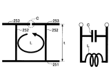
- FIG. 1 is an explanatory diagram for explaining the basic principle of a reflectarray. As shown in the figure, it is assumed that the phase of the reflected wave by each of the plurality of elements aligned on the ground plane gradually changes between adjacent elements. In the case of the illustrated example, the phase difference of the reflected wave by each adjacent element is 90 degrees. Since radio waves travel in a direction perpendicular to the equiphase surface (shown by broken lines), a reflective array is formed by arranging elements two-dimensionally while appropriately adjusting the reflection phase from each element. Thus, the incident wave can be reflected in a desired direction.
- Fig. 2 shows a mushroom structure that can be used as an element for a reflectarray.
- the mushroom structure includes a ground plate 151, a via 152, and a patch 153.
- the ground plate 151 is a conductor that supplies a common potential to a large number of mushroom structures.
- ⁇ x and ⁇ y indicate an interval in the x-axis direction and an interval in the y-axis direction between vias in adjacent mushroom structures, respectively.
- ⁇ x and ⁇ y represent the size of the ground plate 151 corresponding to one mushroom structure.
- the ground plate 151 is as large as an array of many mushroom structures.
- the via 152 is provided to electrically short-circuit the ground plate 151 and the patch 153.
- the patch 153 has a length of Wx in the x-axis direction and a length of Wy in the y-axis direction.
- the patch 153 is provided in parallel to the ground plate 151 at a distance t, and is short-circuited to the ground plate 151 through the via 152.
- t For simplicity of illustration, only two mushroom structures are shown in FIG. 2, but the reflect array has a large number of such mushroom structures in the x-axis and y-axis directions.
- each element constituting the reflect array has a mushroom structure.
- the reflect array may be formed of any element that reflects radio waves.
- a ring-shaped conductive pattern (Fig. 3 (1)), a cross-shaped conductive pattern (Fig. 3 (2)), and a plurality of parallel conductive patterns (Fig. 3 (3 )) Etc.
- a structure (FIG. 3 (4)) without a via connecting the patch and the ground plate may be used.
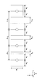
- FIG. 4 shows an enlarged plan view of the reflect array as shown in FIG. Four patches 153 arranged in a line along the line p and four patches 143 arranged along the line q adjacent to the line are shown. The number of patches is arbitrary.
- FIG. 5 shows a state in which a number of elements as shown in FIGS. 2 and 4 are aligned on the xy plane to form a reflectarray.
- Fig. 6 shows the equivalent circuit of the mushroom structure shown in Fig. 2, Fig. 4 and Fig. 5.
- Capacitance C is generated due to a gap between the mushroom-structured patch 153 aligned along the line p in FIG. 4 and the mushroom-structured patch 153 aligned along the line q.
- an inductance L is generated due to the mushroom structure vias 152 arranged along the line p and the mushroom structure vias 152 arranged along the line q. Therefore, the equivalent circuit of the adjacent mushroom structure is a circuit as shown on the right side of FIG. That is, in the equivalent circuit, the inductance L and the capacitance C are connected in parallel.
- Capacitance C, inductance L, surface impedance Zs, and reflection coefficient ⁇ can be expressed as follows.
- Equation (1) ⁇ 0 represents the dielectric constant of vacuum, and ⁇ r represents the relative dielectric constant of the material interposed between the patches.
- the element interval is the via interval ⁇ y in the y-axis direction.
- the gap g y is a gap between adjacent patches.
- g y ⁇ y ⁇ Wy.
- Wy represents the length of the patch in the y-axis direction. That is, the argument of the arccosh function represents the ratio between the element spacing and the gap.
- ⁇ represents the magnetic permeability of the material interposed between the vias
- t represents the height of the patch 153 (distance from the ground plate 151 to the patch 153).
- ⁇ represents an angular frequency
- j represents an imaginary unit.
- Equation (4) ⁇ represents free space impedance, and ⁇ represents a phase difference.
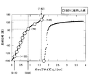
- FIG. 7 shows the relationship between the size Wy of the mushroom structure patch as shown in FIGS. 2, 4 and 5 and the reflection phase.
- the reflection phase of the mushroom structure becomes zero at a certain resonance frequency.
- the capacitance C and / or inductance L of the element it is possible to adjust the reflection phase when the element reflects the radio wave of the resonance frequency.
- the design of the reflect array it is necessary to appropriately set the reflection phase of each element by the capacitance C and / or the inductance L so that the radio wave of the resonance frequency is reflected in a desired direction.
- solid lines indicate theoretical values, and those plotted with circles indicate simulation values by finite element method analysis.
- t02 represents a graph when the distance t is 0.2 mm.
- t08 represents a graph when the distance t is 0.8 mm.
- t16 represents a graph when the distance t is 1.6 mm.
- t24 represents a graph when the distance t is 2.4 mm.
- the via spacing or element spacing ⁇ x and ⁇ y is 2.4 mm as an example.
- the reflection phase can be around 175 degrees by setting the thickness to 0.2 mm. However, even if the patch size Wy changes from 0.5 mm to 2.3 mm, the difference in the reflection phase becomes 1 degree or less, and the value of the reflection phase hardly changes. From the graph t08, the phase can be around 160 degrees by setting the thickness to 0.8 mm. At this time, when the patch size Wy changes from 0.5 mm to 2.3 mm, the reflection phase changes from about 162 degrees to 148 degrees, but the change range is as small as 14 degrees.
- the phase is 145 degrees or less, and when the patch size Wy changes from 0.5 mm to 2.1 mm, the reflection phase decreases only slowly from 144 degrees to 107 degrees.
- the reflection phase decreases rapidly.
- the reflection phase is 54 degrees for the simulation value (circle) and 0 degree for the theoretical value (solid line). Reach.
- the patch size Wx in the x-axis direction is the same for all elements, and the patch size Wy in the y-axis direction varies depending on the location of the element. .
- only the patch size Wy in the y-axis direction needs to be determined according to the location of the element, simplifying the design. become.
- one of the various via heights or substrate thicknesses t to be used in the design (e.g., t24) is selected, and the size of each of the multiple patches to be aligned is required at the position of the patch. It is determined according to the reflection phase. For example, when t24 is selected and the required reflection phase is 72 degrees at a certain patch position, the patch size Wy is about 2 mm. Similarly, the sizes of other patches are determined. Ideally, it is preferable that the patch size is designed so that the change of the reflection phase by the entire element group aligned in the reflect array is 360 degrees.
- the reflected wave is in the direction in which the reflection phase changes in the zx plane, that is, the y-axis Tilt in a direction perpendicular to or transverse to the direction (x-axis direction).
- Controlling the reflected wave in this way is referred to as “horizontal control” for convenience.
- the present invention is not limited to horizontal control.
- a reflect array is configured with the structure shown in FIG.
- the patch size and gap can be determined by several methods.
- the element spacing ⁇ x may be common and the individual patches may be asymmetric as shown in FIG. 9, or the individual patches may be symmetric and the element spacing may be different as shown in FIG.
- the element spacing ⁇ x may be common and individual patches may be designed symmetrically.
- the gap g x in the x-axis direction strongly affects the reflected wave when the radio wave having the electric field component in the x-axis direction is reflected in the desired direction.
- the radio wave having an electric field component in the x-axis direction is a TE wave (Transverse Electric wave) or a horizontal Polarization.
- horizontal polarization is a radio wave having an electric field component parallel to the incident surface or the ground (xy plane).
- the radio wave When a radio wave having an electric field component in the y-axis direction enters the reflect array for horizontal control as shown in FIGS. 4 and 5, for example, along the z-axis, the radio wave is reflected at a desired reflection angle on the zx plane.
- the reflection phase of the element is determined by the capacitance C and inductance L of the element, and in particular, the capacitance C is determined by the gap or gap between the patches.
- the gap g y in the y-axis direction is set to various values according to various reflection phase values, and the gap g x in the x-axis direction is kept constant. ing.
- the gap g y in the y-axis direction has a strong influence on the reflected wave.
- the radio wave having an electric field component in the y-axis direction is a TM wave (Transverse Magnetic wave) or a vertical wave.
- Polarization “Vertical polarization” in this case is a radio wave having an electric field component perpendicular to the incident surface or the ground (xy plane).
- the gap g x in the x-axis direction is designed so that the TE wave reflects in the desired direction
- the TM wave It can be seen that the gap g y in the y-axis direction should be designed so that is reflected in the desired direction.
- the desired direction of the TE wave and the desired direction of the TM wave may be the same or different.
- the frequencies of the TE wave and TM wave may be the same or different. The case where the frequencies of the TE wave and TM wave are different will be described later in ⁇ 3. This will be described in “Multi-band shared polarization>”.
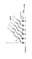
- FIG. 13 shows an element array for one cycle of a reflect array that reflects TE waves and TM waves in the same direction.
- a plurality of element rows for one cycle shown in the figure are arranged in the x-axis and y-axis directions.
- FIG. 14 is a plan view of two element rows arranged in the y-axis direction in the reflect array in which many element rows for one period shown in FIG. 13 are arranged.
- FIG. 15 shows the values of various parameters for each of the ten elements shown in FIGS. Specifically, the dimension of the gap g y in the y-axis direction, the reflection phase corresponding to the gap g y (that is, the reflection phase for TM waves), the dimension of the gap g x in the x-axis direction, and the gap g x Specific numerical values of the reflected phase (that is, the reflected phase with respect to the TE wave), the patch size Wy in the y-axis direction, and the patch size Wx in the x-axis direction are shown.
- the phase difference of the reflected wave by each adjacent element is 36 degrees (2 ⁇ / 10 radians).
- the difference in reflection phase by each adjacent element is a divisor that is an integral multiple of 360 (for example, 36 degrees).
- the reflection phase difference it is not essential that the reflection phase difference exactly matches a divisor that is an integral multiple of 360. It is only necessary that the reflection phase difference substantially matches.
- 27 is not strictly a divisor of 360, but by arranging 13 elements while changing the reflection phase difference by 27 degrees, the range of the reflection phase of 360 degrees can be substantially covered.
- a reflection phase difference such as 27 degrees may be used.
- FIG. 16A shows a simulation result regarding the reflect array including the element arrays shown in FIG. 13-15.
- ⁇ i and ⁇ r are declinations made by the incident wave and the reflected wave with respect to the z axis
- ⁇ i and ⁇ r are made by the incident wave and the reflected wave with respect to the x axis. Declination.
- E ⁇ represents the electric field component in the ⁇ direction of the reflected radio wave
- E ⁇ represents the electric field component in the ⁇ direction of the reflected radio wave.
- the number of elements for one period for reflecting the TE wave in the desired direction and the number of elements for one period for reflecting the TM wave in the desired direction are both ten.
- the number of elements N TE for one period for reflecting the TE wave may be different from the number of elements N TM for one period for reflecting the TM wave.
- the number of elements N TE for one cycle for reflecting TE wave is 10
- element number N TM of one cycle for reflecting TM waves may be 20.
- the phase difference between the reflected waves by the adjacent elements is 36 degrees (360 ⁇ 10) for the TE wave and 18 degrees (360 ⁇ 20) for the TM wave.
- the TE wave and the TM wave are made in the same direction. Or it can reflect as intended in different directions.
- the x-axis direction and the y-axis direction are only relative directions when defining a two-dimensional plane.
- the reflect array is in the xy plane.
- the TE wave has an electric field component that changes in the x-axis direction
- the TM wave has an electric field component that changes in the y-axis and z-axis directions. Therefore, the reflect array can be created by designing the gap g x in the x-axis direction to reflect the TE wave and designing the gap g y in the y-axis direction to reflect the TM wave. This is the same as the above example. However, in the example shown in FIG.
- the TE wave has an electric field component that changes in the y-axis direction
- the TM wave has an electric field component that changes in the x-axis and z-axis directions.
- the reflected wave of the TE wave is greatly affected by the gap g y in the y-axis direction
- the reflected wave of the TM wave is greatly affected by the gap g x in the x-axis direction. Therefore, in the example shown in FIG.
- ⁇ r indicates the relative dielectric constant of the dielectric substrate interposed between the patch and the ground plane.
- c indicates the speed of light.
- the plasma frequency f p satisfies the following relationship with the plasma wave number k p .
- ⁇ ZZ indicates the effective dielectric constant of the metal medium along the via, and is represented by the following formula (10).
- epsilon h represents the relative dielectric constant of the substrate constituting the mushroom
- eta 0 indicates the impedance of free space.
- k 0 indicates the wave number of the free space
- k indicates the wave number of the mushroom medium, and is expressed by the following formula (11).
- k z represents the z component of the wave vector (wave vector), and is represented by the following formula (12).
- Equation (5) Z g represents surface impedance and satisfies the relationship of the following equation.
- ⁇ eff represents an effective impedance expressed by the following formula (14), and ⁇ is a grid parameter expressed by the following formula (15).
- FIG. 18 shows the reflection phase of a reflected wave as a function of frequency when a TE wave and a TM wave are incident on a reflect array in which elements are aligned at equal intervals in the x-axis direction and the y-axis direction.
- the relative dielectric constant ⁇ r of the substrate is 4.5
- the via height (that is, the distance between the ground plane and the patch) t is 1.52 mm
- the element spacing ⁇ x in the x-axis direction is 4.1 mm.
- the element spacing ⁇ y in the y-axis direction is also 4.1 mm.
- the reflection phase gradually decreases from 150 degrees when the frequency increases from 5 GHz, the reflection phase becomes 0 when the frequency is 9 GHz (f M ), and the frequency As the value increases, the reflection phase decreases.
- the reflection phase decreases rapidly from 150 degrees when the frequency increases from 5 GHz, the reflection phase becomes 0 when the frequency is 8.25 GHz (f L ), and the reflection phase increases as the frequency increases.
- the frequency decreases and the frequency exceeds 10 GHz
- the reflection phase reaches about -180 degrees.
- the reflection phase becomes +180 degrees, and decreases rapidly.
- the reflection phase becomes 0, and as the frequency further increases, the reflection phase decreases.
- a TM wave there are two frequencies (f L , f H ) at which the reflection phase is 0 degrees.
- Such a decrease is referred to as bi-resonance or spurious resonance.
- the reflection phase of the mushroom structure (element) becomes 0 at the resonance frequency, and by adjusting the capacitance C and / or the inductance L of the plurality of elements constituting the reflect array, the radio wave of the resonance frequency is generated. It can be reflected in a desired direction.
- the gap g x in the x-axis direction is designed to appropriately reflect the TE wave of the first frequency
- the gap g y in the y-axis direction is designed to appropriately reflect the TM wave of the second frequency.
- the gap g x in the x-axis direction strongly influences the reflected wave, while the y-axis
- the gap g y in the y-axis direction has a dominant influence on the reflected wave. This is the same in the case of multiband.
- FIG. 19 shows the relationship between the gap size g y in the y-axis direction and the reflection phase of an element having a mushroom structure.
- the radio wave is a TM wave
- the incident angle ⁇ i is 20 degrees.
- the shape of the graph shown is merely an example, and other values are used when other parameter values are used.
- FIG. 20 shows the relationship between the gap size g x in the x-axis direction and the reflection phase of a mushroom structure element.
- the radio wave is a TE wave
- the incident angle ⁇ i is 20 degrees.
- the shape of the illustrated graph is merely an example, and other shapes are used when other parameter values are used.
- the gap g x in the x-axis direction is designed to appropriately reflect the TE wave of the first frequency f L , and the TM wave of the second frequency f H is appropriately reflected. It is necessary to design the gap g y in the y-axis direction.
- the reflection phase to be realized with respect to the TM wave by a certain element is determined, and the value of the gap size g y in the y-axis direction corresponding to the reflection phase is obtained in the graph shown in FIG.
- the gap size g x in the x-axis direction and the reflection phase are determined using a graph when the gap size in the y-axis direction is g y .
- the gap sizes g x and g y of individual elements can be determined. For example, FIG.
- the gap size g y in the y-axis direction is 0.15 mm.
- the gap size g x in the x-axis direction and the reflection phase are determined using a graph when the gap size g y in the y-axis direction is 0.15 mm.
- the gap size g y in the y-axis direction is 0.89 mm.
- the gap size g x in the x-axis direction and the reflection phase are determined using a graph when the gap size g y in the y-axis direction is 0.89 mm.
- the gap size g y in the y-axis direction is 1.62 mm.
- the gap size g x in the x-axis direction and the reflection phase are determined using a graph when the gap size g y in the y-axis direction is 1.62 mm.
- the method of determining the gap sizes g x , g y and the reflection phase is merely an example, and the gap sizes g x , g y and the reflection phase may be determined by any appropriate method.
- ⁇ 3.2 Period boundary Configure the reflect array by changing the gap size g x and g y between the element patches along the x-axis direction and gradually changing the reflection phase of the TE and TM waves along the x-axis direction. In this case, it is difficult to change the reflection phase also in the y-axis direction. Therefore, it is desirable that the element array for one period constituting the reflect array is formed by a plurality of elements arranged in a line in the x-axis direction, and the reflect array is formed by positioning a large number of the element arrays. By setting the periodic boundaries in the element rows in this way, the design of the reflect array can be greatly simplified.
- the incident direction and the reflection direction of radio waves are set as shown in FIG. 17A.
- the origin corresponds to one element in the reflectarray.
- the incident unit vector u i along the direction in which the incident wave travels can be written as follows.
- Reflecting unit vector u r along the direction in which the reflected wave travels can be written as follows.
- the center coordinates of each of the plurality of elements constituting the reflect array are (m ⁇ x, n ⁇ y, 0).
- N x is the maximum value of m
- N y is the maximum value of n.
- the position vector r mn of the mth element in the x-axis direction and the nth element in the y-axis direction (referred to as the mnth element for convenience) can be written as follows.
- r mn (m ⁇ x, n ⁇ y, 0) (19)
- the reflection phase ⁇ mn (f) to be realized by the mn-th element can be written as follows.
- ⁇ mn (f) (2 ⁇ f / c) (r mn ⁇ u i ⁇ r mn ⁇ u r ) + 2 ⁇ N (20)
- “ ⁇ ” represents an inner product of vectors.
- 2 ⁇ N 0, generality is not lost.
- ⁇ mn (f) can be set to an arbitrary value by Equation (21).
- the difference in reflection phase ( ⁇ mn (f) - ⁇ m-1n ( It is preferable that f) or ⁇ mn (f) - ⁇ mn-1 (f)) is a divisor (eg, 36 degrees) that is an integral multiple of 360.
- the reflection phase ⁇ mn (f) to be realized by the mn-th element generally depends on ⁇ x and ⁇ y. However, in Equation (21), if, when that is multiplied by ⁇ y (sin ⁇ i sin ⁇ i -sin ⁇ r sin ⁇ r) was equal to identically 0, the reflection phase alpha mn (f) is independent of the [Delta] y No longer. In this case, the reflection phase ⁇ mn (f) gradually changes in the x-axis direction, but can be made constant in the y-axis direction. In this way, the reflection array to be realized by each element changes in the x-axis direction but is constant in the y-axis direction, so that the reflect array can be easily realized.
- the deflection angle ⁇ r of the reflected wave from the z-axis can be uniquely determined based on the deflection angle ⁇ r of the reflected wave from the x-axis.
- Equation (25) or Equation (27) the TE wave and TM wave reflection phases gradually change along the x-axis direction, but along the y-axis direction. It is possible to prevent the reflection phase from changing.
- the element array for one cycle that composes the reflect array can be formed by a plurality of elements arranged in a line in the x-axis direction. By setting such a periodic boundary, the design of the reflect array is greatly simplified.
- the reflection phase ⁇ mn (f) of the mn-th element depends on the frequency f (specifically, ⁇ mn (f) ⁇ f) . Therefore, in general, the reflection phase ⁇ mn (f L ) of the element at the first frequency f L and the reflection phase ⁇ mn (f H ) of the element at the second frequency f H are not the same. Therefore, generally speaking, the direction in which the TE wave of the first frequency f L is reflected by the reflect array and the direction in which the TM wave of the second frequency f H is reflected by the reflect array are controlled independently.
- the reflection phase difference ⁇ x (f L ) for the TE wave of the first frequency f L and the reflection phase difference ⁇ x (f H ) for the TM wave of the second frequency f H are the incidence of the TE wave and the TM wave.
- the direction ( ⁇ i , ⁇ i ) and the desired direction ( ⁇ r , ⁇ r ) are common, they can be written as follows.
- Equation (29) (2 ⁇ f L / c) ⁇ x (sin ⁇ i cos ⁇ i ⁇ sin ⁇ r cos ⁇ r ) (29)
- ⁇ x (f H ) (2 ⁇ f H / c) ⁇ x (sin ⁇ i cos ⁇ i ⁇ sin ⁇ r cos ⁇ r )
- ⁇ x (f L ): ⁇ x (f H ) f L : f H (31) That is, the ratio of the reflection phase difference ⁇ x (f L ) for the TE wave of the first frequency f L and the reflection phase difference ⁇ x (f H ) for the TM wave of the second frequency f H is the first frequency f When equal to the ratio of L and the second frequency f H , the TE wave and the TM wave can be reflected in a common desired direction ( ⁇ r , ⁇ r ).
- the reflection phase difference is 36 degrees
- the reflection phase difference is 27.3 degrees
- 40 elements arranged in a line in the x-axis direction form one period of the reflectarray, and 13 elements for reflecting TE waves are included in one period.
- ten elements for reflecting TM waves can be included for four periods.
- FIG. 22 shows a plan view of an element row for one period of such 40 elements.
- a reflect array can be formed.
- FIG. 23 shows values of various parameters for each of the 40 elements shown in FIG. Specifically, phase for TM wave, dimension of gap g y in y-axis direction, phase for TE wave, dimension of gap g x in x- axis direction, patch size Wy in y-axis direction and patch size Wx in x-axis direction Specific numerical values of are shown.
- the phase difference of the reflected wave by each adjacent element is 36 degrees for the TM wave and 27 degrees for the TE wave.
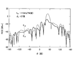
- FIG. 24 is a simulation result showing a radar cross section (RCS) (dB sm ) for a reflect array including a number of element arrays for one period shown in FIGS. 22 and 23.
- the incident and reflected radio waves are 8.25 GHz TE waves.
- the horizontal axis of the graph represents the deviation angle ⁇ from the z axis.
- E ⁇ represents the electric field component in the ⁇ direction of the reflected wave
- E ⁇ represents the electric field component in the ⁇ direction of the reflected wave.
- Equation (22) the reflection phase ⁇ mn (f) to be realized by the element gradually changes in the x-axis direction. However, it is made constant in the y-axis direction. However, the embodiment is not limited to this example, and conversely, the reflection phase ⁇ mn (f) to be realized by the element gradually changes in the y-axis direction but is constant in the x-axis direction. You can also. In that case, in equation (21), the coefficient of ⁇ x (sin ⁇ i cos ⁇ i ⁇ sin ⁇ r cos ⁇ r ) needs to be equal to zero. In this case, the following equation is established.
- the deflection angle ⁇ r of the reflected wave from the z-axis can be uniquely determined from the deflection angle ⁇ r of the reflected wave from the x-axis.
- the reflection phase ⁇ mn (f) to be realized by the mn-th element can be written as follows.
- the difference ⁇ y (f) with respect to the reflection phase ⁇ mn-1 (f) can be written as follows using Equation (21).
- the ratio of the reflection phase difference ⁇ y (f L ) for the TE wave of the first frequency f L and the reflection phase difference ⁇ y (f H ) for the TM wave of the second frequency f H is the first frequency f
- the TE wave and the TM wave can be reflected in a common desired direction ( ⁇ r , ⁇ r ).
- the reflection phase by an arbitrary element (mn) among the plurality of elements constituting the reflect array is expressed by the first axis (
- the reflection phase of the element adjacent to the mn-th element in the (x-axis or y-axis) direction differs from the reflection phase by a predetermined value, but is equal to the reflection phase of the element adjacent to the element in the second axis (y-axis or x-axis) direction It can be said.
- the magnitude of the second axial component of the incident unit vector u i is equal to the magnitude of the second axial component of the reflected unit vector u r, and can be said.
- the ratio of the reflection phase difference ⁇ x or y (f L ) for the TE wave of the first frequency f L and the reflection phase difference ⁇ x or y (f H ) for the TM wave of the second frequency f H is When the ratio is equal to the ratio between the frequency f L of 1 and the second frequency f H , the TE wave and the TM wave can be reflected in a common desired direction ( ⁇ r , ⁇ r ).
- FIG. 28 shows an explanatory diagram for explaining the basic principle of the reflectarray.
- the phase of the reflected wave by each of the plurality of elements aligned on the ground plane gradually changes between adjacent elements.
- the phase difference of the reflected wave by each adjacent element is 90 degrees. Since radio waves travel in a direction perpendicular to the equiphase surface (shown by the broken line), a reflective array is formed by arranging the elements on a plane while appropriately adjusting the reflection phase from each element. The incident wave can be reflected in a desired direction.
- the phase ⁇ mn given to the mn-th element in the design of the reflect array configured by the M ⁇ N array is expressed by the equation (40) using the position vector r mn and the incident and reflection direction unit vectors u i and ur. (Non-Patent Document 2).
- (40) as in equation when participate the reflection phase of alpha mn to mn th element a plane perpendicular to the unit vector u r of the reflecting direction becomes equiphase surface, the reflected wave in the direction of u r Advances.
- k f is a wave number at the operating frequency f and is represented by the equation (41).
- Equation (42) the phase difference between the mn-th and (m ⁇ 1) n-th elements adjacent in the x direction is Equation (42), and the phase difference between the elements adjacent in the y direction is Equation (43). Given.
- phase difference between the mn-th and m (n ⁇ 1) -th elements adjacent in the y direction is given by equation (42), and the phase difference between the elements adjacent in the y direction is given by expression (43).
- the unit vector u i can circle the incident direction and the unit vector u r can circle reflection direction of the plane formed is obtained as a plane formed by the two straight lines. This is called a reflective surface.
- the electric field is orthogonal to the reflecting surface, it is called a TE wave, and when it is parallel, it is called a TM wave.
- phase difference with respect to TE incidence is ⁇ mxTE and ⁇ nyTE TM
- the phase difference with respect to ⁇ mxTE and ⁇ nyTM is set to ⁇ mxTM , ⁇ nyTM
- the formulas (44) and (45) hold both the TE wave and TM wave It can be seen that the incident wave can be reflected in the same direction from the direction.
- equations (46) and (47) may be modified to make the phase ratio and the wave number ratio equal. At this time, if the phase ratio is the same from the equations (42) and (43), the phase difference ratio is also equal. That is, equation (48) may be established.
- Equation (48) indicates that both the phase difference ratio in the Y direction and the phase difference ratio in the X direction are frequency ratios.
- Equation (49) in order to reflect each in the same direction when the first frequency is TM incident and the second frequency is TM incident, Equation (49) may be established.
- equation (50) may be established.
- equation (51) In order to reflect each in the same direction when the first frequency is TE incident and the second frequency is TM incident, equation (51) may be established.
- the equation (52) may be established.
- the TE incidence It can be seen that the ratio of the phase obtained at the first frequency at this time, the ratio of the phase obtained at the second frequency at the time of TM incidence, and the ratio of wave numbers should be equal.
- FIG. 29 shows an equivalent circuit of a mushroom structure.
- Capacitance C occurs due to the gap between the patches 253 of the mushroom structure in FIG. Therefore, when the mushroom structure patches 253 arranged along the line p in FIG. 29 and the mushroom structure patches arranged along the line q are arranged in the mushrooms having different gap sizes, the capacitances C1,. Will line up along line q.
- an inductance L is generated due to the mushroom structure via 252 aligned along the line p and the mushroom structure via 252 aligned along the line q. Therefore, the equivalent circuit of the adjacent mushroom structure is a circuit as shown on the right side of FIG. That is, in the equivalent circuit, the inductance L and the capacitance C are connected in parallel. Capacitance C is expressed by equations (53) and (54).
- Equation (53) is a capacitance generated when the electric field is parallel to the x direction
- Equation (54) is a capacitance generated when the electric field is parallel to the y direction.
- the capacitance of the mushroom structure can be changed by changing the value of the gap.
- the patch size in the x direction changes, which affects the capacitance in the y direction. That is, there arises a problem that the capacitance value cannot be determined independently in the x and y directions.
- Equations (53) and (54) ⁇ 0 represents the dielectric constant of the vacuum, and ⁇ r represents the relative dielectric constant of the material interposed between the patches.
- the element interval is the via interval ⁇ y in the y-axis direction.
- the gap g y is a gap between adjacent patches.
- g y ⁇ y ⁇ Wy.
- Wy represents the length of the patch in the y-axis direction. That is, the argument of the arccosh function represents the ratio between the element spacing and the gap.
- the inductance L, the surface impedance Zs, and the reflection coefficient ⁇ are expressed by the equations (55), (56), and (57), respectively.
- Equations (53) and (54) ⁇ 0 represents the dielectric constant of the vacuum, and ⁇ r represents the relative dielectric constant of the material interposed between the patches.
- Wy represents the length of the patch in the y-axis direction, and Wx represents the length of the patch in the x-axis direction. That is, the argument of the arccosh function represents the ratio between the element spacing and the gap.
- ⁇ represents the magnetic permeability of the material interposed between the vias
- t represents the height of the patch 253 (the distance from the ground plate 251 to the patch 253).
- ⁇ represents an angular frequency
- j represents an imaginary unit.
- Equation (57) ⁇ represents free space impedance, and ⁇ represents a phase difference.
- the reflection phase of the mushroom structure becomes 0 at a certain resonance frequency. Since the resonance frequency is shifted by adjusting the capacitance C and / or the inductance L of the element, the value of the reflection phase can be adjusted.
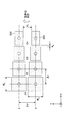
- FIG. 31A and 31B are diagrams illustrating the structure of an H-type mushroom element according to an embodiment of the present invention.
- an H-type mushroom element according to an embodiment of the present invention includes a ground plate 251, a via 252, and an H-type patch 254.
- each H-type mushroom element has a via 252 and an H-type patch 254, and a plurality of H-type mushroom elements are arranged on the ground plate 251 in an array.
- the H-type patch 254 is composed of three rectangular parts, two rectangular outer patches of the same size and one rectangular inner patch, and the H-type patch 254 is defined by one side of the rectangle.
- the two outer patches are connected to the inner patch so as to sandwich the inner patch so as to be symmetric with respect to the first direction (X direction) and the second direction (Y direction) orthogonal to the first direction.
- the length of the outer patch in the X direction is Ox
- the length of the H-type patch in the Y direction is Oy
- the length of the inner patch in the X direction is Ix
- the inner patch The length in the Y direction of the patch is Iy.
- the H-shaped patch has an H-shaped shape as shown in FIGS. 31 and 32.
- the H-shaped patch according to the present invention is not limited to this, for example, two outer patches. May have different sizes.
- the H-type patch may be asymmetric with respect to the first direction and the second direction. Further, the first direction and the second direction described above do not necessarily have to be orthogonal.
- the H-type patch 254 is composed of three rectangular portions of two rectangular outer patches of the same size and one rectangular inner patch, and the H-type patch is defined by one side of the rectangle.
- the patch is an arbitrary shape in which two outer patches are connected to the inner patch so as to sandwich the inner patch so as to be symmetric with respect to one direction and a second direction orthogonal to the first direction.
- the patches of the reflecting elements shown in FIGS. 33 to 37 have shapes defined in this way, and are all H-type patches.
- Ox> Ix In a typical H-type patch, Ox> Ix.
- the present invention is not limited to this, and Ox ⁇ Ix may be satisfied.
- the reflect array according to each embodiment of the present invention is configured by arranging a plurality of H-type mushroom elements having the above-described H-type patch in an array.
- the length of Oy is changed for the incidence of an electric field parallel to the Y direction, and the length of Ox is constant for the incidence of an electric field parallel to the X direction.
- the H-type mushroom element is arranged so as to change only the value of Ix. If Ox is considered to correspond to the area of the capacitor forming the capacitance (capacitance) in the X direction, that is, Wx in the equation (53), the value of Ox does not change even if Ix is changed.
- the second By changing the value of the gap between the inner patches generated between the inner patches in the direction, the reflection phase with respect to the polarization in the second direction can be changed.
- the capacitance generated between the H-type elements adjacent in the first direction is determined based on the size of the cap between the first outer patches
- the capacitance generated between the H-type elements adjacent in the second direction is It will be determined based on the size of the gap between the second outer patches.
- the H-shaped patch is composed of the four outer vertices of the H-shaped patch composed of two rectangular outer patches and the inner four vertices composed of the inner patches, and is incident in parallel to the first direction.
- the length of the inner patch in the first direction determined by the position of the four vertices of the inner patch is maintained while maintaining the position of the four vertices of the outer patch and the size of the outer patch constant. It is determined. Further, in order to change the reflection phase of the electric field incident in parallel with the second direction, the length in the second direction determined by the positions of the four vertices of the outer patch of the H-type patch in the second direction is determined.
- FIG. 38 is a diagram showing the relationship between the reflection phase and the length of the outer patch in the first embodiment of the present invention.
- the simulation results regarding the relationship between the reflection phase of the electric field incident in parallel to the Y direction and Oy are shown for three bands of 8.25 GHz, 11 GHz, and 14.3 GHz.
- FIG. 39 is a diagram showing the relationship between the reflection phase and the length of the inner patch in the first embodiment of the present invention.
- the outer patch length Oy in the Y direction is 2.8 mm and 3.9 mm
- the simulation result regarding the relationship between the reflection phase of the electric field incident in parallel to the X direction and Iy is shown.
- the value of Iy is also determined.
- the value of the reflection phase can be changed by nearly 360 degrees by changing Ix.
- the reflection phase of TE (Transverse Electric wave) incidence can be changed independently of the reflection phase of TM (Transverse Magnetic wave) incidence.
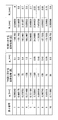
- Table 1 in FIG. 40 shows design values of the reflect array using the H-type mushroom element according to the first embodiment of the present invention.
- the values of Oy and Ix were determined so as to satisfy Table 1 from FIGS.
- FIG. 41 shows the selected value of Oy
- FIG. 42 shows the selected value of Ix.
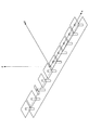
- FIG. 33 is an overall view of the reflect array using the H-type mushroom element according to the first embodiment of the present invention, whose structure is determined from FIGS. 38 and 39 so that the reflection phase can be obtained based on the design values shown in Table 1. is there.
- FIGS. 34 to 37 are enlarged views of the reflect array using the H-type mushroom element.
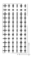
- the multiband reflectarray according to the first embodiment is configured by arranging H-type mushroom elements of various sizes in an array.
- FIGS. 34 to 37 an enlarged view of each part of the multiband reflectarray shown in FIG. 33 is shown.
- a total of 30 H-type mushroom elements, 3 in the X direction and 10 in the Y direction, are arranged in an array, with different Oy 1 -Oy 10 and Ix 1 -Ix 10
- a set 211 of 10 H-type mushroom elements having a size and the same Ox size are arranged in the Y direction.
- Similar array sets 212 and 213 of H-type mushroom elements are arranged in the X direction.
- a total of 30 H-type mushroom elements, 3 in the X direction and 10 in the Y direction, are arranged in an array, and different Oy 11 ⁇
- a set 221 of ten H-type mushroom elements having the size of Oy 20 and Ix 11 -Ix 20 and the same size of Ox is arranged in the Y direction.
- Similar array sets 222, 223 of H-type mushroom elements are arranged in the X direction.
- a total of 30 H-type mushroom elements, 3 in the X direction and 10 in the Y direction, are arranged in an array, and different Oy 21 ⁇
- a set 231 of ten H-type mushroom elements having the sizes of Oy 30 and Ix 21 -Ix 30 and the same size of Ox is arranged in the Y direction.
- Similar array sets 232 and 233 of H-type mushroom elements are arranged in the X direction.
- a total of 30 H-type mushroom elements, 3 in the X direction and 10 in the Y direction, are arranged in an array, and different Oy 31 ⁇
- a set 241 of ten H-type mushroom elements having the size of Oy 40 and Ix 31 -Ix 40 and the same size of Ox is arranged in the Y direction.
- Similar array sets 242 and 243 of H-type mushroom elements are arranged in the X direction.
- FIG. 43 and 44 show the scattering cross sections when the light enters the reflect array under the design conditions shown in Table 1.
- FIG. 45 is an enlarged view of a reflect array using an H-type mushroom element according to the second embodiment of the present invention.
- the size of Iy is variable, but as shown in FIG. 45, in the multiband reflectarray according to the second embodiment, Iy is set to a constant size.
- FIG. 46 is a diagram showing a change with respect to Oy of the reflection phase characteristic of the multiband reflectarray by the TE incident H type mushroom element according to the second embodiment of the present invention.
- Oy when Oy is changed while Iy is kept constant, even if the length of Ix is changed to 2 mm and 3.7 mm, a simulation result is obtained in which the value of the reflection phase shows a substantially similar curve. It has been. That is, it can be understood that the reflection phase can be determined by the length of Oy with respect to the incidence of the electric field parallel to the Y direction without depending on the length of Ix.
- FIG. 47 is a diagram showing a change with respect to Ix of the reflection phase characteristic of the multiband reflectarray by the TM incident H type mushroom element according to the second embodiment of the present invention.
- Ix is changed while Ox is kept constant, even if the length of Oy is changed to 3 mm and 3.7 mm, a simulation result is obtained in which the value of the reflection phase shows a substantially similar curve. It has been. That is, for the incidence of an electric field parallel to the X direction, the reflection phase can be determined by the length of Ix without depending on the length of Oy.
- FIG. 48 is an enlarged view of a reflect array using an H-type mushroom element according to the third embodiment of the present invention.
- the multiband reflectarray according to the third embodiment for the incidence of an electric field parallel to the X direction, the length of Ix is changed while the length of Ox is kept constant, and the incidence of the electric field parallel to the Y direction is performed.
- the H-type mushroom element is arranged to change the length of Oy while keeping the length of Iy constant. That is, each H-type mushroom element has the same size of Ox and Iy and different sizes of Ix and Oy.
- each H-type mushroom element has the same Ox, different Oy and Ix, and the same Iy. This makes it possible to change the reflection phase of TE incidence independently of the reflection phase of TM incidence, as in the first embodiment, and the electric field incident parallel to the X direction as described above with reference to FIG.
- the graphs showing the relationship between the reflection phase and Iy can be made to overlap each other.
Abstract
本発明の1つの態様は、アレー状に配置された複数の素子を有するリフレクトアレーであって、各素子は、接地プレートから隔てて設けられたH型パッチを有し、前記H型パッチは、2つの矩形の外側パッチによって構成されるH型パッチの外側の4つの頂点と、内側パッチによって構成される内側の4つの頂点によって構成され、第1方向に平行に入射した電界の反射位相を変えるため、前記外側パッチの4つの頂点の位置と外側パッチの大きさを一定に維持しながら、前記内側パッチの4つの頂点の位置によって決まる前記第1方向の内側パッチの長さが決定され、前記第2方向に平行に入射した電界の反射位相を変えるため、前記第2方向に関する前記H型パッチの外側パッチの4つの頂点の位置によって決まる前記第2方向の長さが決定されるリフレクトアレーに関する。
Description
本発明は、無線通信に利用されるリフレクトアレーに関する。
無線通信の技術分野において、通信エリアの確保等のために、入射波を自在な方向に向けて散乱できるリフレクトアレーの適用が検討されている。また、リフレクトアレーは、直接波がドミナントである見通し伝搬環境において、複数の(マルチ)パスを形成し、複数入力複数出力(Multiple Input Multiple Output:MIMO)方式によるスループットの向上及び/又は信頼性の強化を図る等のために使用されてもよい。
また、通信の高速大容量化等を図るため、互いに直交する2つの偏波が、偏波ダイバーシチや、偏波MIMOとして、通信に利用される場合がある。この場合における偏波は直線偏波であり、例えば、入射面に垂直な電界成分を有する電波(Transverse Electric wave:TE波)及び入射面に平行な電界成分を有する電波(Transverse Magnetic wave:TM波)のように言及されてもよい。あるいは偏波は大地に垂直な電界成分を有する垂直偏波(vertical polarization wave)及び大地に平行な電界成分を有する水平偏波(horizontal polarization wave)のように言及されてもよい。また、特に屋外においては、伝搬環境の影響により電界はさまざまな方向に回転する。この場合、電界は、垂直成分と水平成分の二つの成分を持つと考えてよい。何れにせよ、電界の振幅方向が互いに直交する2つの平面波は通信に利用可能である。しかしながら、従来のリフレクトアレーは、ある方向から到来する2つの偏波をそれぞれ所望の方向に反射させることは困難であった。
他方、ロングタームエボリューション(Long Term Evolution:LTE)アドバンスト(LTEアドバンスト)方式のような無線通信システムでは、必要に応じて通信に複数の周波数バンド又はキャリアが使用される。従って、通信に使用される電波を反射するリフレクトアレーも複数の周波数バンド(マルチバンド)に対応していることが望ましい。マルチバンドに対応した従来のリフレクトアレーについては、非特許文献1に記載されている。非特許文献1に記載のリフレクトアレーは、Kaバンド(32GHz)用の途切れた環状の素子と、Xバンド(8.4GHz)用の途切れた方形の線状素子と、Cバンド(7.1GHz)用のクロスダイポール素子とを有する。しかしながら、このリフレクトアレーは円偏波を対象としており、直線偏波用にそのまま利用することはできない。更に非特許文献1に記載のリフレクトアレーは、Ka、X及びCバンドで適切に動作するように素子を複雑な形状に加工する必要があり、コスト高となってしまうおそれがある。
従来のリフレクトアレーは、非特許文献2にあるように、マイクロストリップ素子のように、約半波長の素子を用いている。この素子のサイズを変えることによって、共振周波数がずれるため、反射位相を変化させることができる。よって、平面波が所望方向に向くように各アレー素子の位相を決定すればよい。このような、半波長の素子を複数の偏波に対応させ、ある方向から到来する2つの偏波をそれぞれ所望の方向に反射させるリフレクトアレーを実現するために、クロスダイポールを用いる方法が報告されている(非特許文献3,4)。
一方、従来の半波長素子を用いたリフレクトアレーよりも反射方向を広角に制御する方法として、波長よりもはるかに小さい、マッシュルーム構造を用いたリフレクトアレーが報告されている(非特許文献5)。しかし、二つの直交する偏波を共用できるマッシュルーム構造はいままで存在しなかった。従って、広角制御できる偏波共用のためのマッシュルーム構造は存在しなかった。
他方、LTE(Long Term Evolution)-Advanced方式のような無線通信システムでは、必要に応じて通信に複数の周波数バンド又はキャリアが使用される。従って、通信に使用される電波を反射するリフレクトアレーも複数の周波数バンド(マルチバンド)に対応していることが望ましい。マルチバンドに対応した従来のリフレクトアレーについては、以下の非特許文献1及び非特許文献3に記載されている。非特許文献1に記載のリフレクトアレーは、Kaバンド(32GHz)用の途切れた環状の素子と、Xバンド(8.4GHz)用の途切れた方形の線状素子と、Cバンド(7.1GHz)用のクロスダイポール素子とを有する。非特許文献3に記載のリフレクトアレーは、クロスダイポールを素子とし、電界がX軸に平行な第一の周波数f1の入射波については、クロスダイポール素子のX方向の長さを変化させて反射位相が決定され、電界がY軸に平行な第二の周波数f2の入射波電波については、クロスダイポール素子のY方向の長さを変化させて反射位相を決定する。
しかし、従来の構造は、半波長素子をベースにしており、グレーティングローブの発生や素子間相互結合の影響により、40度以上の広角制御が困難である。
このような問題を解決するため、非特許文献5、6に記載されるようなマッシュルーム構造を有したリフレクトアレーが提案された。しかし、これらは偏波共用素子ではない。このため、各偏波に対して独立に設計することは困難である。従って、Y方向のマッシュルーム間のギャップgyを変化させると、X方向のマッシュルーム間のギャップgxに対する反射位相の値もまた変化してしまうことがわかる。
Fan Yang, Ang Yu, Atef Elsherbeni and John Huang,"Single-Layer Multi-band Circularly Polarized Reflect array Antenna: Concept, Design and Measurement,"URSI General Assembly, Chicago, Illinois, August 7-16, 2008.
D. M. Pozar, T. S. Targonsky, and H. D. Syrigos, "Design ofmillimeter wave microstrip reflectarrays," IEEE Trans. Antennas Propagat., vol.AP-45, no. 2, pp. 287-295, 1997.
T. Maruyama, T. Furuno, T. Ohya, Y. Oda, Q. Chen, and K. Sawaya,"Dual Frequency Selective Reflectarray for Propagation Improvement", IEEE iWAT,2010, pp.1-4, 5464764, March 2010.
L. Li, Q. Chen, Q. Yuan, K. Sawaya, T. Maruyama, T. Furuno, and SUebayashi, "Frequency Selective Reflectarray using Crossed-Dipole Elements withSquare Loops for Wireless Communication Applications," IEEE Trans. AntennasPropagat., vol. AP-59, no. 1, pp. 89-99, 2011.
T. Maruyama, T. Furuno, Y. Oda, J. Shen, and T. Ohya, "Capacitancevalue control for metamaterial reflectarray using multi-layer mushroomstructure with parasitic patches," ACES JOURNAL, vol. 27, no. 1, pp. 28-41,Jan. 2012.
T. Maruyama, J. Shen, N. Tran and Y. Oda "Multi-band Reflectarrayusing Mushroom Structure," IEEE ICWITS 2012.
T. Maruyama, Y. Oda, J. Shen, N. Tran and H. Kayama, "Design of wideangle reflection reflectarray using multi-layer mushroom structure to improvepropagation," IEEE URSI General Assembly and Scientific Symposium, 2011 XXXthURSI, Aug., 2011.
J. Shen, Y. Oda, T. Furuno, T. Maruyama, and T. Ohya, "A novelapproach for capacity improvement of 2x2 MIMO in LOS channel usingreflectarray," VTC2011 spring, 10.1109/VETECS.2011.5956339, May 2011.
Payam Nayeri, Fan Yang, and Atef Z. Elsherbeni, "Single-FeedMulti-Beam Reflectarray Antennas, IEEE AP-S 2010.
本発明の1つの課題は、マッシュルーム素子を有するリフレクトアレーにおいて、基板の表面に平行な電界成分を有する第1の偏波及び基板の表面に垂直な電界成分を有する第2の偏波を所望の方向に反射することが可能であり、かつ簡易な構造のリフレクトアレーを提供することである。
本発明の他の課題は、従来困難であった、課題を解決するためになされたものであり、
(1)TE入射の反射位相とTM入射の反射位相とを独立に変更することを可能にするリフレクトアレーを提供すること、
(2)広角制御を可能にすること、
(3)マッシュルーム構造において、X方向の反射位相をかえるためにX方向のギャップサイズを変化させたとき、Y方向の容量(キャパシタンス)の値を変化させない方法を提供すること、
(4)複数の周波数での共用
のうちの全て、もしくはどれか一つを可能とするリフレクトアレーを実現することである。
(1)TE入射の反射位相とTM入射の反射位相とを独立に変更することを可能にするリフレクトアレーを提供すること、
(2)広角制御を可能にすること、
(3)マッシュルーム構造において、X方向の反射位相をかえるためにX方向のギャップサイズを変化させたとき、Y方向の容量(キャパシタンス)の値を変化させない方法を提供すること、
(4)複数の周波数での共用
のうちの全て、もしくはどれか一つを可能とするリフレクトアレーを実現することである。
上記課題を解決するため、本発明の1つの態様は、アレー状に配置された複数の素子を有するリフレクトアレーであって、各素子は、接地プレートから隔てて設けられたH型パッチを有し、前記H型パッチは、2つの矩形の外側パッチによって構成されるH型パッチの外側の4つの頂点と、内側パッチによって構成される内側の4つの頂点によって構成され、第1方向に平行に入射した電界の反射位相を変えるため、前記外側パッチの4つの頂点の位置と外側パッチの大きさを一定に維持しながら、前記内側パッチの4つの頂点の位置によって決まる前記第1方向の内側パッチの長さが決定され、前記第2方向に平行に入射した電界の反射位相を変えるため、前記第2方向に関する前記H型パッチの外側パッチの4つの頂点の位置によって決まる前記第2方向の長さが決定されるリフレクトアレーに関する。
本発明の他の態様は、アレー状に配置された複数の反射素子を有するリフレクトアレーであって、各反射素子は、接地プレートから隔てて設けられたH型パッチを有し、前記H型パッチは、同一サイズの2つの矩形の外側パッチと、1つの矩形の内側パッチとを有し、前記2つの外側パッチは、矩形の一辺により規定される第1方向と前記第1方向に直交する第2方向とに関して前記H型パッチが対称となるように、前記内側パッチを挟むように前記内側パッチに連結され、前記第1方向に平行に入射した電界を偏波するため、前記第2方向に配置される各反射素子の外側パッチの前記第1方向に関する長さを一定にしたまま、前記第1方向に関する前記内側パッチの長さが決定され、前記第2方向に平行に入射した電界を偏波するため、前記第2方向に関する前記H型パッチの長さが決定されるリフレクトアレーに関する。
本発明の上記態様によると、マッシュルーム素子を有するリフレクトアレーにおいて、基板の表面に平行な電界成分を有する第1の偏波及び基板の表面に垂直な電界成分を有する第2の偏波を所望の方向に反射することが可能であり、かつ簡易な構造のリフレクトアレーを提供することが可能である。
また、本発明の上記態様によると、TE入射の反射位相とTM入射の反射位相とを独立に変更することを可能にするリフレクトアレーを、さらには、複数の周波数で共用可能なリフレクトアレーを提供することができる。
添付図面を参照しながら以下の観点から実施形態を説明する。図中、同様な要素には同じ参照番号又は参照符号が付されている。
以下の実施例では、アレー状に配置された複数の素子を有するリフレクトアレーが開示される。アレー状に配置された複数の素子の各素子は、接地プレートから隔てて設けられたH型パッチを有する。H型パッチは、2つの矩形の外側パッチによって構成されるH型パッチの外側の4つの頂点と、内側パッチによって構成される内側の4つの頂点によって構成される。開示されるリフレクトアレーでは、第1方向に平行に入射した電界の反射位相を変えるため、外側パッチの4つの頂点の位置と外側パッチの大きさを一定に維持しながら、内側パッチの4つの頂点の位置によって決まる第1方向の内側パッチの長さが決定される。また、第2方向に平行に入射した電界の反射位相を変えるため、第2方向に関するH型パッチの外側パッチの4つの頂点の位置によって決まる第2方向の長さが決定される。
他の実施例では、アレー状に配置された複数の反射素子の各反射素子は、接地プレートから隔てて設けられたH型パッチを有する。H型パッチは、同一サイズの2つの矩形の外側パッチと、1つの矩形の内側パッチとを有し、2つの外側パッチは、矩形の一辺により規定される第1方向と第1方向に直交する第2方向とに関してH型パッチが対称となるように、内側パッチを挟むように内側パッチに連結される。開示されるリフレクトアレーでは、第1方向に平行に入射した電界を偏波するため、第2方向に配置される各反射素子の外側パッチの第1方向に関する長さを一定にしたまま、第1方向に関する前記内側パッチの長さが決定される。また、第2方向に平行に入射した電界を偏波するため、第2方向に関するH型パッチの長さが決定される。
まず、本発明の第1実現形態によるリフレクトアレーを説明する。
1.リフレクトアレー
2.偏波共用シングルバンド
3.偏波共用マルチバンド
3.1 二共振
3.2 周期境界
3.3 反射方向
4.変形例
これらの項目の区分けは本発明に本質的ではなく、2以上の項目に記載された事項が必要に応じて組み合わせて使用されてよいし、ある項目に記載された事項が、別の項目に記載された事項に(矛盾しない限り)適用されてよい。
2.偏波共用シングルバンド
3.偏波共用マルチバンド
3.1 二共振
3.2 周期境界
3.3 反射方向
4.変形例
これらの項目の区分けは本発明に本質的ではなく、2以上の項目に記載された事項が必要に応じて組み合わせて使用されてよいし、ある項目に記載された事項が、別の項目に記載された事項に(矛盾しない限り)適用されてよい。
<1.リフレクトアレー>
図1は、リフレクトアレーの基本原理を説明するための説明図を示す。図示されているように、地板上に整列した複数の素子各々による反射波の位相が、隣接する素子同士の間で徐々に変化していたとする。図示の例の場合、隣接する素子各々による反射波の位相差は90度である。電波は等位相面(破線で示されている)に垂直な方向に進行するので、個々の素子からの反射位相を適切に調整しつつ、素子を二次元的に配置することでリフレクトアレーを形成し、入射波を所望の方向に反射させることができる。
図1は、リフレクトアレーの基本原理を説明するための説明図を示す。図示されているように、地板上に整列した複数の素子各々による反射波の位相が、隣接する素子同士の間で徐々に変化していたとする。図示の例の場合、隣接する素子各々による反射波の位相差は90度である。電波は等位相面(破線で示されている)に垂直な方向に進行するので、個々の素子からの反射位相を適切に調整しつつ、素子を二次元的に配置することでリフレクトアレーを形成し、入射波を所望の方向に反射させることができる。
図2は、リフレクトアレー用の素子として使用可能なマッシュルーム構造を示す。マッシュルーム構造は、接地プレート151と、ビア152と、パッチ153とを有する。接地プレート151は、多数のマッシュルーム構造に対して共通の電位を供給する導体である。Δx及びΔyは、隣接するマッシュルーム構造におけるビア間のx軸方向の間隔及びy軸方向の間隔をそれぞれ示す。Δx及びΔyは、マッシュルーム構造1つ分に対応する接地プレート151のサイズを表す。一般に、接地プレート151は多数のマッシュルーム構造が並んだアレイと同程度に大きい。ビア152は、接地プレート151とパッチ153とを電気的に短絡するために設けられる。パッチ153は、x軸方向にWxの長さを有し、y軸方向にWyの長さを有する。パッチ153は、接地プレート151に対して平行に距離tを隔てて設けられ、ビア152を介して接地プレート151に短絡される。図示の簡明化のため、図2ではマッシュルーム構造が2つしか示されていないが、リフレクトアレーには、このようなマッシュルーム構造がx軸及びy軸方向に多数設けられている。
図2に示す例の場合、リフレクトアレーを構成する個々の素子はマッシュルーム構造で構成されている。しかしながらこのことは実施の形態に必須ではない。電波を反射する任意の素子でリフレクトアレーが形成されてよい。例えば、正方形のパッチの代わりに、リング状の導電性パターン(図3(1))、十字型の導電性パターン(図3(2))、並列的な複数の導電性パターン(図3(3))等を有する素子が使用されてもよい。また、マッシュルーム構造において、パッチと接地プレートとを接続するビアがない構造(図3(4))が使用されてもよい。ただし、上記のように素子にマッシュルーム構造を採用することは、小さな反射素子を簡易に設計できる等の観点から好ましい。
図4は、図2に示されているようなリフレクトアレーの拡大平面図を示す。線pに沿って一列に並んだ4つのパッチ153と、その列に隣接して線qに沿って並んだ4つのパッチ143とが示されている。パッチの数は任意である。図5は図2及び図4に示すような素子がxy平面上に多数整列してリフレクトアレーを形成している様子を示す。
図6は、図2、図4、図5に示すマッシュルーム構造の等価回路を示す。図4の線pに沿って並ぶマッシュルーム構造のパッチ153と、線qに沿って並ぶマッシュルーム構造のパッチ153との間のギャップに起因して、キャパシタンスCが生じる。更に、線pに沿って並ぶマッシュルーム構造のビア152、及び線qに沿って並ぶマッシュルーム構造のビア152に起因して、インダクタンスLが生じる。したがって、隣接するマッシュルーム構造の等価回路は、図6右側に示されるような回路になる。すなわち、等価回路において、インダクタンスLとキャパシタンスCとが並列に接続されている。キャパシタンスC、インダクタンスL、表面インピーダンスZs及び反射係数Γは、次のように表すことができる。

図7は、図2、図4及び図5に示すようなマッシュルーム構造のパッチのサイズWyと反射位相との関係を示す。概して、マッシュルーム構造(素子)の反射位相は、ある共振周波数において0になる。素子のキャパシタンスC及び/又はインダクタンスLを調整することで、素子が共振周波数の電波を反射する際の反射位相を調整することができる。リフレクトアレーの設計においては、共振周波数の電波が所望方向に反射するように、キャパシタンスC及び/又はインダクタンスLにより個々の素子の反射位相を適切に設定する必要がある。図中、実線は理論値を示し、丸印でプロットされているものは有限要素法解析によるシミュレーション値を示す。図7は、4種類のビアの高さ又は基板の厚みtの各々について、パッチのサイズWyと反射位相との関係を示す。t02は距離tが0.2mmである場合のグラフを表す。t08は距離tが0.8mmである場合のグラフを表す。t16は距離tが1.6mmである場合のグラフを表す。t24は距離tが2.4mmである場合のグラフを表す。ビア間隔又は素子間隔Δx及びΔyは、一例として2.4mmである。
グラフt02より、厚さを0.2mmとすることにより、反射位相を175度の周辺にできることがわかる。しかし、パッチのサイズWyが0.5mmから2.3mmまで変化しても、反射位相の差は1度以下となり、反射位相の値はほとんど変化しない。グラフt08より、厚さを0.8mmとすることにより、位相を160度の周辺とすることができる。またこのとき、パッチのサイズWyが0.5mmから2.3mmまで変化すると、反射位相は約162度から148度まで変化するが、変化の範囲は14度と、小さい。グラフt16より、厚さを1.6mmとすると位相は145度以下となり、パッチのサイズWyが0.5mmから2.1mmに変化する場合、反射位相は144度から107度に緩慢にしか減少していないが、サイズWyが2.1mmより大きくなると、反射位相は急激に減少し、サイズWyが2.3mmの場合に、反射位相は、シミュレーション値(丸印)で54度及び理論値(実線)で0度に達する。グラフt24の場合、パッチのサイズWyが0.5mmから1.7mmに変化する場合、反射位相は117度から90度に緩慢にしか減少していないが、サイズWyが1.7mmより大きくなると、反射位相は急激に減少し、サイズWyが2.3mmの場合に、反射位相は、-90度に達する。
図2、図4及び図5に示すようなマッシュルーム構造で素子を形成する場合、x軸方向のパッチサイズWxは全ての素子で同一であり、y軸方向のパッチサイズWyが素子の場所によって異なる。しかしながら、パッチサイズWxが全ての素子で共通することは必須ではなく、素子毎に異なるように設計することも可能である。ただし、パッチサイズWxが全ての素子で同一であるマッシュルーム構造を用いてリフレクトアレーを設計する場合、y軸方向のパッチサイズWyのみを、素子の場所に応じて決定すればよいので、設計が簡易になる。具体的には、様々なビアの高さ又は基板の厚みtの内、設計に使用するもの(例えば、t24)を選択し、整列する複数のパッチ各々のサイズが、そのパッチの位置で必要な反射位相に応じて決定される。例えば、t24が選択されていた場合において、あるパッチの位置で必要な反射位相が72度であった場合、パッチのサイズWyは約2mmである。同様にして、他のパッチについてもサイズが決定される。理想的には、リフレクトアレーの中で整列している1つの素子群全体による反射位相の変化が360度であるように、パッチサイズが設計されていることが好ましい。
ところで、図4及び図5に示す構造において、電界の振幅方向がy軸方向である電波がリフレクトアレーに入射した場合、反射波はzx面内で反射位相が変化している方向、すなわちy軸方向に対して垂直方向又は横方向(x軸方向)に傾く。このようにして反射波を制御することを便宜上「水平制御」と言及する。しかしながら本発明は水平制御に限定されない。例えば、図4及び図5に示す構造の代わりに、図8に示すような構造でリフレクトアレーを構成し、電界の振幅方向がx軸方向である電波を、電界の方向に対して平行に反射させる、すなわち縦方向(x軸方向)に傾けることが可能である。このようにして反射波を制御することを便宜上「垂直制御」と言及する。垂直制御を行う場合において、パッチサイズとギャップはいくつかの方法によって決めることができる。例えば、図9に示すように素子の間隔Δxを共通とし且つ個々のパッチを非対称にしてもよいし、図10に示すように個々のパッチを対称にし且つ素子の間隔を異ならせてもよいし、図11に示すように素子の間隔Δxを共通とし且つ個々のパッチを対称に設計してもよい。これらは一例に過ぎず、適切な如何なる方法でパッチサイズ及びギャップが決定されてもよい。
<2.偏波共用シングルバンド>
図8-11に示すような垂直制御用のリフレクトアレーに、x軸方向の電界成分を有する電波が例えばz軸に沿って入射すると、zx面で所望の反射角で電波が反射する。上述したように、素子の反射位相は、素子のキャパシタンスC及びインダクタンスLにより決定され、特にキャパシタンスCはパッチ同士の間の隙間又はギャップにより決定される。垂直制御の場合、図8-11に示すようにx軸方向のギャップgxが様々な反射位相の値に応じて様々な値に設定され、y軸方向のギャップgyは一定に維持されている。このことから、x軸方向の電界成分を有する電波を所望方向に反射させる際、x軸方向のギャップgxが反射波に強く影響している、と言える。図12に示すように、xy面内で規定されるリフレクトアレーに、yz面内を進行する電波が入射する場合、x軸方向の電界成分を有する電波は、TE波(Transverse Electric wave)又は水平偏波である。この場合における「水平偏波」は入射面又は大地(xy平面)に対して平行な電界成分を有する電波である。
図8-11に示すような垂直制御用のリフレクトアレーに、x軸方向の電界成分を有する電波が例えばz軸に沿って入射すると、zx面で所望の反射角で電波が反射する。上述したように、素子の反射位相は、素子のキャパシタンスC及びインダクタンスLにより決定され、特にキャパシタンスCはパッチ同士の間の隙間又はギャップにより決定される。垂直制御の場合、図8-11に示すようにx軸方向のギャップgxが様々な反射位相の値に応じて様々な値に設定され、y軸方向のギャップgyは一定に維持されている。このことから、x軸方向の電界成分を有する電波を所望方向に反射させる際、x軸方向のギャップgxが反射波に強く影響している、と言える。図12に示すように、xy面内で規定されるリフレクトアレーに、yz面内を進行する電波が入射する場合、x軸方向の電界成分を有する電波は、TE波(Transverse Electric wave)又は水平偏波である。この場合における「水平偏波」は入射面又は大地(xy平面)に対して平行な電界成分を有する電波である。
図4及び図5に示すような水平制御用のリフレクトアレーに、y軸方向の電界成分を有する電波が例えばz軸に沿って入射すると、zx面で所望の反射角で電波が反射する。上述したように、素子の反射位相は、素子のキャパシタンスC及びインダクタンスLにより決定され、特にキャパシタンスCはパッチ同士の間の隙間又はギャップにより決定される。水平制御の場合、図4及び図5に示すようにy軸方向のギャップgyが様々な反射位相の値に応じて様々な値に設定され、x軸方向のギャップgxは一定に維持されている。このことから、y軸方向の電界成分を有する電波を所望方向に反射させる際、y軸方向のギャップgyが反射波に強く影響している、と言える。図12に示すように、xy面内で規定されるリフレクトアレーに、yz面内を進行する電波が入射する場合、y軸方向の電界成分を有する電波は、TM波(Transverse Magnetic wave)又は垂直偏波である。この場合における「垂直偏波」は入射面又は大地(xy平面)に対して垂直な電界成分を有する電波である。
以上の考察から、同じ方向から到来するTE波及びTM波を所望方向にそれぞれ反射させるためには、TE波が所望方向に反射するようにx軸方向のギャップgxを設計し、かつTM波が所望方向に反射するようにy軸方向のギャップgyを設計すればよいことが分かる。TE波の所望方向とTM波の所望方向は同一であってもよいし、異なっていてもよい。TE波及びTM波の周波数は、同一でもよいし、異なっていてもよい。TE波及びTM波の周波数が異なる場合については、後述する<3.偏波共用マルチバンド>において説明する。
図13は、TE波及びTM波を同一方向に反射させるリフレクトアレーの1周期分の素子列を示す。実際のリフレクトアレーは、図示の1周期分の素子列が、x軸及びy軸方向に複数個配置されている。図14は、図13に示す1周期分の素子列が多数並んでいるリフレクトアレーにおいて、y軸方向に並ぶ2つの素子列の平面図を示す。
図15は図13及び図14に示す10個の素子各々の各種のパラメータの値を示す。具体的には、y軸方向のギャップgyの寸法、そのギャップgyに対応する反射位相(すなわち、TM波に対する反射位相)、x軸方向のギャップgxの寸法、そのギャップgxに対応する反射位相(すなわち、TE波に対する反射位相)、y軸方向のパッチサイズWy及びx軸方向のパッチサイズWxの具体的な数値が示されている。隣接する素子各々による反射波の位相差は、36度(2π/10ラジアン)である。一般に、ある1周期分の素子列をxy平面上で反復的に設けることでリフレクトアレーを構成する観点からは、隣接する素子各々による反射位相の差分が、360の整数倍の約数(例えば、36度)であることが好ましい。ただし、反射位相差が360の整数倍の約数に厳密に一致することは必須ではなく、実質的に一致していればよい。例えば、27は厳密には360の約数ではないが、反射位相差を27度ずつ変化させながら13個の素子を並べることで、実質的に360度の反射位相の範囲をカバーすることができるので、27度のような反射位相差が使用されてもよい。
図16Aは図13-15に示す素子列で構成されるリフレクトアレーに関するシミュレーション結果を示す。TE波及びTM波の何れについても、電波の入射方向は(θi,φi)=(20度,270度)であり、所望の反射方向は(θr,φr)=(48度,27度)である。ただし、図17Aに示すように、θi及びθrは入射波及び反射波がz軸に対してなす偏角であり、φi及びφrは入射波及び反射波がx軸に対してなす偏角である。図中、Eθは反射された電波のθ方向の電界成分を示し、Eφは反射された電波のφ方向の電界成分を示す。図示のシミュレーション結果は、θ=48度の面内における電波の散乱断面積(dB)を示す。何れの電界成分も、所望方向φ=27度において強いピークを示している。図16Bも同様なシミュレーション結果を示すが、φ=27度の面内における電波の散乱断面積を示す点が異なる。図示されているように、何れの電界成分も、所望方向θ=48度において強いピークを示している。図16A及び図16Bに示すように、このリフレクトアレーは、(θi,φi)=(20度,270度)から到来したTE波及びTM波を、(θr,φr)=(48度,27度)という共通する所望方向に反射できる。
なお、図13-16に示す例では、TE波を所望方向に反射させるための1周期分の素子数とTM波を所望方向に反射させるための1周期分の素子数とが共に10個であったが、このことは実施の形態に必須ではない。TE波を反射させるための1周期分の素子数NTEが、TM波を反射させるための1周期分の素子数NTMと異なってもよい。例えば、TE波を反射させるための1周期分の素子数NTEが10であり、TM波を反射させるための1周期分の素子数NTMが20であってもよい。この場合、隣接する素子各々による反射波の位相差は、TE波については36度(360÷10)であり、TM波については18度(360÷20)となる。
このように、TE波を反射させるためのx軸方向のギャップgx及びTM波を反射させるためのy軸方向のギャップgyを独立に設計することで、TE波及びTM波を同一方向に又は異なる方向に意図したとおりに反射させることができる。
なお、x軸方向及びy軸方向は2次元平面を規定する際の相対的な方向であるにすぎないことに留意を要する。
図17Bは、TE波及びTM波が、φi=270度の方向からリフレクトアレーに入射する様子を示す。リフレクトアレーはxy平面内にある。この場合、TE波はx軸方向に変化する電界成分を有し、TM波はy軸及びz軸方向に変化する電界成分を有する。従って、TE波を反射させるためにx軸方向のギャップgxを設計し、TM波を反射させるためにy軸方向のギャップgyを設計することで、リフレクトアレーを作成できる。この点は上記の例と同様である。しかしながら、図17Cに示す例では、TE波及びTM波が、φi=180度の方向からリフレクトアレーに入射している。この場合、TE波はy軸方向に変化する電界成分を有し、TM波はx軸及びz軸方向に変化する電界成分を有する。この場合、TE波の反射波はy軸方向のギャップgyにより大きな影響を受け、TM波の反射波はx軸方向のギャップgxにより大きな影響を受ける。従って、図17Cに示す例の場合、TE波を反射させるためにy軸方向のギャップgyを設計し、TM波を反射させるためにx軸方向のギャップgxを設計する必要がある。従って、より一般的に言えば、互いに直交する2つの偏波の内の一方を反射させるために、互いに直交する2つの軸方向の内の一方のギャップg1を設計し、他方の偏波を反射させるために、他方の軸方向のギャップg2を設計することで、2つの偏波を各自の所望方向にそれぞれ反射させることができる。
<3.偏波共用マルチバンド>
次に、2つの偏波がそれぞれ異なる周波数を有する場合(マルチバンドの場合)に、それらを同一又は異なる所望方向にそれぞれ反射させるリフレクトアレーを考察する。上述したように、マッシュルーム構造(素子)の反射位相は、ある共振周波数において0になり、その共振周波数の電波を素子が反射する際の反射位相は、キャパシタンスC及び/又はインダクタンスLを調整することで、適切に設定できる。リフレクトアレーの設計においては、共振周波数の電波が所望方向に反射するように、キャパシタンスC及び/又はインダクタンスLにより個々の素子の反射位相を適切に設定する必要がある。
次に、2つの偏波がそれぞれ異なる周波数を有する場合(マルチバンドの場合)に、それらを同一又は異なる所望方向にそれぞれ反射させるリフレクトアレーを考察する。上述したように、マッシュルーム構造(素子)の反射位相は、ある共振周波数において0になり、その共振周波数の電波を素子が反射する際の反射位相は、キャパシタンスC及び/又はインダクタンスLを調整することで、適切に設定できる。リフレクトアレーの設計においては、共振周波数の電波が所望方向に反射するように、キャパシタンスC及び/又はインダクタンスLにより個々の素子の反射位相を適切に設定する必要がある。
<<3.1 二共振>>
図12に示すようにリフレクトアレーにTM波がz軸に対して入射角θiで入射する場合、反射波の反射位相(arg(Γ))は次のように表現できる。
図12に示すようにリフレクトアレーにTM波がz軸に対して入射角θiで入射する場合、反射波の反射位相(arg(Γ))は次のように表現できる。

rf=fp/√εr=(kpc)/√εr・・・(7)
により表現されるものとする。fpはプラズマ周波数を示す。εrはパッチ及び地板の間に介在する誘電体基板の比誘電率を示す。cは光速を示す。プラズマ周波数fpはプラズマ波数kpと次の関係を満たす。
fp=kpc/(2π) ・・・(8)
プラズマ波数kpは素子間隔Δxと次の関係を満たす。
プラズマ波数kpは素子間隔Δxと次の関係を満たす。


従って、異なる偏波の周波数として、0度の反射位相をもたらす周波数fL、fM又はfHを使用することで、異なる周波数の偏波を所望方向にそれぞれ反射させるリフレクトアレーを実現できる。すなわち、第1の周波数のTE波を適切に反射するようにx軸方向のギャップgxを設計し、第2の周波数のTM波を適切に反射するようにy軸方向のギャップgyを設計することで、マルチバンドで2つの偏波を各自の所望方向にそれぞれ反射させることができる。<2.偏波共用シングルバンド>において説明したように、x軸方向の電界成分を有する電波を所望方向に反射させる場合、x軸方向のギャップgxが反射波に支配的に強く影響する一方、y軸方向の電界成分を有する電波を所望方向に反射させる場合、y軸方向のギャップgyが反射波に支配的に強く影響する。マルチバンドの場合もこの点は同じである。以下に説明する例では、TE波の周波数(第1の周波数)がfL=8.25GHzであり、TM波の周波数(第2の周波数)がfH=11GHzであるとするが、このことは必須でない。
図19は、マッシュルーム構造の素子のy軸方向のギャップサイズgyと反射位相との間の関係を示す。図19において電波はTM波であり、入射角θiは20度である。図示のグラフの形状は単なる一例にすぎず、他のパラメータの値が使用される場合は他の形状になる。図20はマッシュルーム構造の素子のx軸方向のギャップサイズgxと反射位相との間の関係を示す。図20において電波はTE波であり、入射角θiは20度である。図示のグラフの形状も単なる一例にすぎず、他のパラメータの値が使用される場合は他の形状になる。リフレクトアレーを実現する場合、第1の周波数fLのTE波を適切に反射するようにx軸方向のギャップgxを設計し、第2の周波数fHのTM波を適切に反射するようにy軸方向のギャップgyを設計する必要がある。
ギャップサイズgx、gy及び反射位相の決定の仕方の一例として、次のようにすることが考えられる。まず、或る素子でTM波に対して実現すべき反射位相を決定し、図19に示すグラフにおいて、その反射位相に対応するy軸方向のギャップサイズgyの値を求める。次に、図20において、y軸方向のギャップサイズがgyである場合のグラフを用いて、x軸方向のギャップサイズgx及び反射位相を決定する。この手順を反復することで個々の素子のギャップサイズgx及びgyを決定することができる。例えば、TM波に対する反射位相を-150度とする場合、y軸方向のギャップサイズgyは0.15mmであることが図19から分かる。図20において、y軸方向のギャップサイズgyが0.15mmである場合のグラフを用いて、x軸方向のギャップサイズgx及び反射位相が決定される。TM波に対する反射位相を+70度とする場合、y軸方向のギャップサイズgyは0.89mmであることが図19から分かる。図20において、y軸方向のギャップサイズgyが0.89mmである場合のグラフを用いて、x軸方向のギャップサイズgx及び反射位相が決定される。TM波に対する反射位相を+140度とする場合、y軸方向のギャップサイズgyは1.62mmであることが図19から分かる。図20において、y軸方向のギャップサイズgyが1.62mmである場合のグラフを用いて、x軸方向のギャップサイズgx及び反射位相が決定される。このようなギャップサイズgx、gy及び反射位相の決定の仕方は単なる一例にすぎず、適切な如何なる方法でギャップサイズgx、gy及び反射位相が決定されてもよい。
<<3.2 周期境界>>
素子のパッチ間のギャップサイズgx及びgyをx軸方向に沿って変化させ、TE波及びTM波の反射位相がx軸方向に沿って徐々に変化するようにすることでリフレクトアレーを構成する場合、反射位相をy軸方向にも変化させることは困難である。従って、リフレクトアレーを構成する1周期分の素子列が、x軸方向に1列に並ぶ複数の素子により形成され、その素子列を多数は位置することでリフレクトアレーを形成することが望ましい。このように素子列に周期境界を設定することで、リフレクトアレーの設計を大幅に簡易化できる。
素子のパッチ間のギャップサイズgx及びgyをx軸方向に沿って変化させ、TE波及びTM波の反射位相がx軸方向に沿って徐々に変化するようにすることでリフレクトアレーを構成する場合、反射位相をy軸方向にも変化させることは困難である。従って、リフレクトアレーを構成する1周期分の素子列が、x軸方向に1列に並ぶ複数の素子により形成され、その素子列を多数は位置することでリフレクトアレーを形成することが望ましい。このように素子列に周期境界を設定することで、リフレクトアレーの設計を大幅に簡易化できる。
以下、そのような周期境界を設定するための条件を導出する。
電波の入射方向及び反射方向が図17Aに示すように設定されているとする。図示の例の場合、入射波は(rθφ)極座標において、θ=θi及びφ=φiの方向から到来し、反射波はθ=θr及びφ=φrの方向へ進んでいる。原点はリフレクトアレーにおける1つの素子に対応する。入射波が進行する方向に沿う入射単位ベクトルuiは、次のように書ける。
ui=(uix,uiy,uiz)=(sinθicosφi,sinθisinφi,cosθi) ・・・(17)
反射波が進行する方向に沿う反射単位ベクトルurは、次のように書ける。
反射波が進行する方向に沿う反射単位ベクトルurは、次のように書ける。
ur=(urx,ury,urz)=(sinθrcosφr,sinθrsinφr,cosθr) ・・・(18)
図21に示すように、リフレクトアレーを構成する複数の素子各々の中心座標が、(mΔx,nΔy,0)にあるとする。ただし、m=0,1,2,...Nx及びn=0,1,2,...Nyであり、Nxはmの最大値及びNyはnの最大値である。x軸方向にm番目及びy軸方向にn番目の素子(便宜上、mn番目の素子と言及する)の位置ベクトルrmnは、次のように書ける。
rmn=(mΔx,nΔy,0) ・・・(19)
この場合、mn番目の素子で実現すべき反射位相αmn(f)は、次のように書ける。
αmn(f)=(2πf/c)(rmn・ui-rmn・ur)+2πN ・・・(20)
ただし、「・」はベクトルの内積を表す。cは光速を表し、fは電波の周波数(f=c/λ)を表し、λは電波の波長を表す。(20)式に(17)-(19)式を代入すると、mn番目の素子で実現すべき反射位相αmn(f)は、次のように書ける。
αmn(f)=(2πf/c)(mΔxsinθicosφi+nΔysinθisinφi
-mΔxsinθrcosφr-nΔysinθrsinφr)
=(2πf/c)mΔx(sinθicosφi-sinθrcosφr)
+(2πf/c)nΔy(sinθisinφi-sinθrsinφr)・・・(21)
ただし、2πN=0であるとしたが、一般性は失われない。なお、αmn(f)は数式(21)により任意の値に設定可能である。しかしながら、ある1周期分の素子配列をxy平面上で反復的に設けることでリフレクトアレーを構成する観点からは、隣接する素子各々による反射位相の差分(αmn(f)-αm-1n(f)又はαmn(f)-αmn-1(f))が、360の整数倍の約数(例えば、36度)であることが好ましい。
数式(21)を参照するに、mn番目の素子で実現すべき反射位相αmn(f)は、一般的には、Δx及びΔyに依存している。しかしながら、数式(21)において、仮に、Δyに乗算されている(sinθisinφi-sinθrsinφr)が恒等的に0に等しかったとすると、反射位相αmn(f)はΔyには依存しなくなる。その場合、反射位相αmn(f)は、x軸方向に徐々に変化するが、y軸方向には一定であるようにできる。このように、個々の素子で実現すべき反射位相が、x軸方向には変化するがy軸方向には一定であるようにすることで、リフレクトアレーを簡易に実現できる。
Δyに乗算されている(sinθisinφi-sinθrsinφr)が0に等しい場合、次式が成立する。
sinθisinφi=sinθrsinφr ・・・(22)
これは、図17Aにおいて入射波の入射単位ベクトルuiのy成分の大きさと反射波の反射単位ベクトルurのy成分の大きさとが等しいことを示す。すなわち、入射単位ベクトル及び反射単位ベクトルのy成分同士が等しい場合、個々の素子で実現すべき反射位相を、x軸方向に変化させる一方、y軸方向には一定であるようにできる。数式(22)は、次のようにも書ける。
これは、図17Aにおいて入射波の入射単位ベクトルuiのy成分の大きさと反射波の反射単位ベクトルurのy成分の大きさとが等しいことを示す。すなわち、入射単位ベクトル及び反射単位ベクトルのy成分同士が等しい場合、個々の素子で実現すべき反射位相を、x軸方向に変化させる一方、y軸方向には一定であるようにできる。数式(22)は、次のようにも書ける。
sinθr=sinθisinφi/sinφr ・・・(23)
θr=arcsin(sinθisinφi/sinφr) ・・・(24)
従って、反射波のx軸からの偏角φrに基づいて、反射波のz軸からの偏角θrを一意に決定できる。数式(22)-(24)が満たされる場合、mn番目の素子で実現すべき反射位相αmn(f)は、次のように書ける。
θr=arcsin(sinθisinφi/sinφr) ・・・(24)
従って、反射波のx軸からの偏角φrに基づいて、反射波のz軸からの偏角θrを一意に決定できる。数式(22)-(24)が満たされる場合、mn番目の素子で実現すべき反射位相αmn(f)は、次のように書ける。
αmn(f)=(2πf/c)mΔx(sinθicosφi-sinθrcosφr)
=(2πf/c)mΔx[sinθicosφi-(sinθisinφi/sinφr)cosφr] ・・・(25)
従って、mn番目の素子で実現すべき反射位相αmn(f)は、反射波のx軸からの偏角φrにより一意に決定される。
=(2πf/c)mΔx[sinθicosφi-(sinθisinφi/sinφr)cosφr] ・・・(25)
従って、mn番目の素子で実現すべき反射位相αmn(f)は、反射波のx軸からの偏角φrにより一意に決定される。
一例として、入射波のx軸からの偏角φiが270度であったとする。この場合、sinφi=-1及びcosφi=0であるので、次のように書ける。
θr=arcsin(-sinθi/sinφr) ・・・(26)
αmn(f)=(2πf/c)mΔx[(sinθi/sinφr)cosφr] ・・・(27)
このように、数式(25)又は数式(27)が満たされるようにすることで、TE波及びTM波の反射位相がx軸方向に沿って徐々に変化するが、y軸方向に沿っては反射位相が変化しないようにできる。これにより、リフレクトアレーを構成する1周期分の素子配列が、x軸方向に1列に並ぶ複数の素子により形成でき、このような周期境界を設定することで、リフレクトアレーの設計を大幅に簡易化できる。
αmn(f)=(2πf/c)mΔx[(sinθi/sinφr)cosφr] ・・・(27)
このように、数式(25)又は数式(27)が満たされるようにすることで、TE波及びTM波の反射位相がx軸方向に沿って徐々に変化するが、y軸方向に沿っては反射位相が変化しないようにできる。これにより、リフレクトアレーを構成する1周期分の素子配列が、x軸方向に1列に並ぶ複数の素子により形成でき、このような周期境界を設定することで、リフレクトアレーの設計を大幅に簡易化できる。
<<3.3 反射方向>>
数式(21)、(25)及び(27)を参照すると、mn番目の素子の反射位相αmn(f)は周波数fに依存している(具体的には、αmn(f)∝f)。従って、一般的には、第1の周波数fLにおける素子の反射位相αmn(fL)と第2の周波数fHにおける素子の反射位相αmn(fH)とは同一でない。従って一般的に言えば、第1の周波数fLのTE波がリフレクトアレーにより反射される方向と、第2の周波数fHのTM波がそのリフレクトアレーにより反射される方向とは独立に制御される。
数式(21)、(25)及び(27)を参照すると、mn番目の素子の反射位相αmn(f)は周波数fに依存している(具体的には、αmn(f)∝f)。従って、一般的には、第1の周波数fLにおける素子の反射位相αmn(fL)と第2の周波数fHにおける素子の反射位相αmn(fH)とは同一でない。従って一般的に言えば、第1の周波数fLのTE波がリフレクトアレーにより反射される方向と、第2の周波数fHのTM波がそのリフレクトアレーにより反射される方向とは独立に制御される。
以下、TE波及びTM波が同じ方向から入射し、同じ所望方向(θr,φr)に反射するための条件を考察する。
上記の<<3.2 周期境界>>の検討結果を利用すると、TE波及びTM波の反射位相がx軸方向に沿って徐々に変化するが、y軸方向に沿っては反射位相が変化しないように複数の素子をx軸方向に1列に並べることで、リフレクトアレーの1周期分を形成できる。ただし、隣接する素子による反射位相差は、周波数に応じて異なる値をとる。
座標が(mΔx,nΔy,0)であるmn番目の素子による反射位相αmn(f)と、座標が((m-1)Δx,nΔy,0)であるm-1n番目の素子による反射位相αm-1n(f)との間の差分Δαx(f)は、数式(21)により、次のように書ける。
Δαx(f)=αmn(f)-αm-1n(f)
=(2πf/c)mΔx(sinθicosφi-sinθrcosφr)
+(2πf/c)nΔy(sinθisinφi-sinθrsinφr)
-(2πf/c)(m-1)Δx(sinθicosφi-sinθrcosφr)
-(2πf/c)nΔy(sinθisinφi-sinθrsinφr)
=(2πf/c)Δx(sinθicosφi-sinθrcosφr)・・・(28)
従って、第1の周波数fLのTE波に対する反射位相差Δαx(fL)及び第2の周波数fHのTM波に対する反射位相差Δαx(fH)は、TE波及びTM波の入射方向(θi,φi)及び所望方向(θr,φr)が共通する場合、それぞれ次のように書ける。
Δαx(fL)=(2πfL/c)Δx(sinθicosφi-sinθrcosφr)・・・(29)
Δαx(fH)=(2πfH/c)Δx(sinθicosφi-sinθrcosφr)・・・(30)
数式(29)と数式(30)の比を算出すると、次式が得られる。
Δαx(fH)=(2πfH/c)Δx(sinθicosφi-sinθrcosφr)・・・(30)
数式(29)と数式(30)の比を算出すると、次式が得られる。
Δαx(fL):Δαx(fH)=fL:fH・・・(31)
すなわち、第1の周波数fLのTE波に対する反射位相差Δαx(fL)及び第2の周波数fHのTM波に対する反射位相差Δαx(fH)の比率が、第1の周波数fL及び第2の周波数fHの比率に等しい場合、TE波及びTM波を共通する所望方向(θr,φr)に反射させることができる。
すなわち、第1の周波数fLのTE波に対する反射位相差Δαx(fL)及び第2の周波数fHのTM波に対する反射位相差Δαx(fH)の比率が、第1の周波数fL及び第2の周波数fHの比率に等しい場合、TE波及びTM波を共通する所望方向(θr,φr)に反射させることができる。
例えば、目下の例の場合、第1の周波数はfL=8.25GHzであり、第2の周波数はfH=11GHzであるので、TM波の場合の隣接する素子の反射位相差Δαx(fH)が36度であったとすると、TE波の場合の隣接する素子の反射位相差Δαx(fL)は、36×8.25/11=約27度となる。27は厳密には360の約数ではないが、反射位相差を27度ずつ変化させながら13個の素子を並べることで、実質的に360度の反射位相の範囲をカバーすることができる。TE波及びTM波の入射方向が(θi,φi)=(20度,270度)であり、反射波の所望方向が(θr,φr)=(48度,27度)であるとする。反射位相差が36度である場合、360度の反射位相の範囲をカバーするのに必要な素子数は、360/36=10個である。反射位相差が27.3度である場合、360度の反射位相の範囲をカバーするのに必要な素子数は、360/27=約13個である。この場合、x軸方向に1列に並ぶ40個の素子でリフレクトアレーの1周期分を形成し、その1周期分の中に、TE波を反射させるための13個の素子が3周期分含まれ、TM波を反射させるための10個の素子が4周期分含まれるようにすることができる。
図22はそのような40個の素子による1周期分の素子列の平面図を示す。このような素子列をx軸方向及びy軸方向に複数個並べることで、リフレクトアレーを形成できる。図23は図22に示す40個の素子各々の各種のパラメータの値を示す。具体的には、TM波に対する位相、y軸方向のギャップgyの寸法、TE波に対する位相、x軸方向のギャップgxの寸法、y軸方向のパッチサイズWy及びx軸方向のパッチサイズWxの具体的な数値が示されている。図示されているように、隣接する素子各々による反射波の位相差は、TM波の場合は36度であり、TE波の場合は27度である。
図24は、図22及び図23に示される1周期分の素子列を多数含むリフレクトアレーに対するレーダー反射断面積(Radar Cross Section:RCS)(dBsm)を示すシミュレーション結果である。入射及び反射する電波は8.25GHzのTE波である。グラフの横軸はz軸からの偏角θを示す。TE波の入射方向は(θi,φi)=(20度,270度)であり、反射波の所望方向は(θr,φr)=(48度,27度)である。Eθは反射波のθ方向の電界成分を示し、Eφは反射波のφ方向の電界成分を示す。図示のRCSは、x軸からの偏角φ=φr=27度の面内(所望方向)における値である。何れの電界成分も所望方向のθ=θr=48度において強いピークを示している。
図25も、図22及び図23に示される1周期分の素子列を多数含むリフレクトアレーに対するレーダー反射断面積RCS(dBsm)を示すシミュレーション結果であるが、入射及び反射する電波が11GHzのTM波である点が異なる。図24の場合と同様に、何れの電界成分も所望方向のθ=θr=48度において強いピークを示している。
図24及び図25が示すように、実施の形態によるリフレクトアレーによれば、第1の周波数fLのTE波及び第2の周波数fHのTM波が共通する入射方向から到来した場合に、それらを共通する所望方向にそれぞれ反射させることができる。
<4.変形例>
上記の<<3.2 周期境界>>の説明では、数式(22)を満たすようにすることで、素子で実現すべき反射位相αmn(f)が、x軸方向には徐々に変化するが、y軸方向には一定であるようにしている。しかしながら実施の形態はこの例に限定されず、逆に、素子で実現すべき反射位相αmn(f)が、y軸方向には徐々に変化するが、x軸方向には一定であるようにもできる。その場合、数式(21)において、Δxの係数である(sinθicosφi-sinθrcosφr)が恒等的に0になる必要がある。この場合、次式が成立する。
上記の<<3.2 周期境界>>の説明では、数式(22)を満たすようにすることで、素子で実現すべき反射位相αmn(f)が、x軸方向には徐々に変化するが、y軸方向には一定であるようにしている。しかしながら実施の形態はこの例に限定されず、逆に、素子で実現すべき反射位相αmn(f)が、y軸方向には徐々に変化するが、x軸方向には一定であるようにもできる。その場合、数式(21)において、Δxの係数である(sinθicosφi-sinθrcosφr)が恒等的に0になる必要がある。この場合、次式が成立する。
sinθicosφi=sinθrcosφr ・・・(32)
これは、図17Aにおいて入射波の入射単位ベクトルuiのx成分と反射波の反射単位ベクトルurのx成分とが等しいことを示す。入射及び反射単位ベクトルのx成分同士が等しい場合に、個々の素子で実現すべき反射位相を、y軸方向に変化させる一方、x軸方向には一定であるようにできる。数式(32)は、次のようにも書ける。
これは、図17Aにおいて入射波の入射単位ベクトルuiのx成分と反射波の反射単位ベクトルurのx成分とが等しいことを示す。入射及び反射単位ベクトルのx成分同士が等しい場合に、個々の素子で実現すべき反射位相を、y軸方向に変化させる一方、x軸方向には一定であるようにできる。数式(32)は、次のようにも書ける。
sinθr=sinθicosφi/cosφr ・・・(33)
θr=arcsin(sinθicosφi/cosφr) ・・・(34)
従って、反射波のx軸からの偏角φrから、反射波のz軸からの偏角θrを一意に決定できる。この場合、mn番目の素子で実現すべき反射位相αmn(f)は、次のように書ける。
θr=arcsin(sinθicosφi/cosφr) ・・・(34)
従って、反射波のx軸からの偏角φrから、反射波のz軸からの偏角θrを一意に決定できる。この場合、mn番目の素子で実現すべき反射位相αmn(f)は、次のように書ける。
αmn(f)=(2πf/c)nΔy(sinθisinφi-sinθrsinφr)
=(2πf/c)nΔy[sinθisinφi-(sinθicosφi/cosφr)sinφr] ・・・(35)
従って、mn番目の素子で実現すべき反射位相αmn(f)は、反射波のx軸からの偏角φrにより一意に決定される。
=(2πf/c)nΔy[sinθisinφi-(sinθicosφi/cosφr)sinφr] ・・・(35)
従って、mn番目の素子で実現すべき反射位相αmn(f)は、反射波のx軸からの偏角φrにより一意に決定される。
更に、座標が(mΔx,nΔy,0)であるmn番目の素子による反射位相αmn(f)と、座標が(mΔx,(n-1)Δy,0)であるmn-1番目の素子による反射位相αmn-1(f)との間の差分Δαy(f)は、数式(21)により、次のように書ける。
Δαy(f)=αmn(f)-αmn-1(f)
=(2πf/c)mΔx(sinθicosφi-sinθrcosφr)
+(2πf/c)nΔy(sinθisinφi-sinθrsinφr)
-(2πf/c)mΔx(sinθicosφi-sinθrcosφr)
-(2πf/c)(n-1)Δy(sinθisinφi-sinθrsinφr)
=(2πf/c)Δy(sinθisinφi-sinθrsinφr)・・・(36)
従って、第1の周波数fLのTE波に対する反射位相差Δαy(fL)及び第2の周波数fHのTM波に対する反射位相差Δαy(fH)は、TE波及びTM波の入射方向(θi,φi)及び所望方向(θr,φr)が共通する場合、それぞれ次のように書ける。
Δαy(fL)=(2πfL/c)Δy(sinθisinφi-sinθrsinφr)・・・(37)
Δαy(fH)=(2πfH/c)Δy(sinθisinφi-sinθrsinφr)・・・(38)
数式(37)と数式(38)の比を算出すると、次式が得られる。
Δαy(fH)=(2πfH/c)Δy(sinθisinφi-sinθrsinφr)・・・(38)
数式(37)と数式(38)の比を算出すると、次式が得られる。
Δαy(fL):Δαy(fH)=fL:fH・・・(39)
従って、第1の周波数fLのTE波に対する反射位相差Δαy(fL)及び第2の周波数fHのTM波に対する反射位相差Δαy(fH)の比率が、第1の周波数fL及び第2の周波数fHの比率に等しい場合、TE波及びTM波を共通する所望方向(θr,φr)に反射させることができる。
従って、第1の周波数fLのTE波に対する反射位相差Δαy(fL)及び第2の周波数fHのTM波に対する反射位相差Δαy(fH)の比率が、第1の周波数fL及び第2の周波数fHの比率に等しい場合、TE波及びTM波を共通する所望方向(θr,φr)に反射させることができる。
よって、上記の<<3.2 周期境界>>及び上記の説明を総合すると、リフレクトアレーを構成する複数の素子のうちの任意の或る素子(mn)による反射位相は、第1の軸(x軸又はy軸)方向においてmn番目の素子に隣接する素子による反射位相と所定値だけ異なる一方、第2の軸(y軸又はx軸)方向においてその素子に隣接する素子による反射位相と等しい、と言える。更に、入射単位ベクトルuiの第2の軸方向成分の大きさは、反射単位ベクトルurの第2の軸方向成分の大きさと等しい、とも言える。更に、第1の周波数fLのTE波に対する反射位相差Δαx又はy(fL)及び第2の周波数fHのTM波に対する反射位相差Δαx又はy(fH)の比率が、第1の周波数fL及び第2の周波数fHの比率に等しい場合、TE波及びTM波を共通する所望方向(θr,φr)に反射させることができる。
次に、本発明の第2実現形態によるリフレクトアレーを説明する。
まず、マッシュルーム構造を有した反射素子によるマルチバンドリフレクトアレーを概略する。
図28は、リフレクトアレーの基本原理を説明するための説明図を示す。図示されているように、地板上に整列した複数の素子各々による反射波の位相が、隣接する素子同士の間で徐々に変化していたとする。図示の例の場合、隣接する素子各々による反射波の位相差は90度である。電波は等位相面(破線で示されている)に垂直な方向に進行するので、個々の素子からの反射位相を適切に調整しつつ、素子を平面上に配置することでリフレクトアレーを形成し、入射波を所望の方向に反射させることができる。
M×Nのアレーによって構成されるリフレクトアレー設計の際にmn番目の素子に与えられる位相αmnは、位置ベクトルrmn、入射及び反射方向単位ベクトルui,urを用いて(40)式で表される(非特許文献2)。いいかえると、(40)式のように、mn番目の素子にαmnの反射位相を与ると、反射方向の単位ベクトルurに直交する面が等位相面となり、urの方向に反射波が進む。


先ずはじめにTE入射とTM入射を同じ方向に反射させるための原理について述べる。TE入射に対する位相差を、ΔαmxTE,ΔαnyTETM入射に対する位相差を、ΔαmxTM,ΔαnyTMとおくと、(44)式、(45)式が成立するとき、TE波も、TM波も同じ方向から入射波を同じ方向に反射できることがわかる。


第一の周波数をf1、第二の周波数をf2とするときに、二つの周波数どうしの入射方向ベクトルuiと位置ベクトルrmnがそれぞれ等しい場合に、二つの周波数ともに同じ反射方向ベクトルurの方向に反射するためには、


(46),(47)式を変形して、位相の比と、波数の比が等しくすればよいことがわかる。また、このとき、(42),(43)式より位相の比が等しければ位相差の比もまた等しくなる。すなわち、(48)式が成り立てばよい。

次に、周波数とTM,TE入射の関係について述べる。ここで、第一の周波数がTM入射、第二の周波数がTM入射のときにそれぞれが同じ方向に反射するようにするためには、(49)式が成り立てばよい。


本発明のH型マッシュルームの動作原理を説明するために、まず従来のマッシュルーム構造の動作原理について説明する。
図29は、マッシュルーム構造の等価回路を示す。図29の並ぶマッシュルーム構造のパッチ253の間のギャップに起因して、キャパシタンスCが生じる。従って図29の線pに沿って並ぶマッシュルーム構造のパッチ253と、線qに沿って並ぶマッシュルーム構造のパッチにより、ギャップの大きさの異なるマッシュルームを並べると、値の異なるキャパシタンスC1,..,Cnが線qに沿って並ぶことになる。更に、線pに沿って並ぶマッシュルーム構造のビア252、及び線qに沿って並ぶマッシュルーム構造のビア252に起因して、インダクタンスLが生じる。したがって、隣接するマッシュルーム構造の等価回路は、図29右側に示されるような回路になる。すなわち、等価回路において、インダクタンスLとキャパシタンスCとが並列に接続されている。キャパシタンスC、は、(53)、(54)式であらわされる。
図29は、マッシュルーム構造の等価回路を示す。図29の並ぶマッシュルーム構造のパッチ253の間のギャップに起因して、キャパシタンスCが生じる。従って図29の線pに沿って並ぶマッシュルーム構造のパッチ253と、線qに沿って並ぶマッシュルーム構造のパッチにより、ギャップの大きさの異なるマッシュルームを並べると、値の異なるキャパシタンスC1,..,Cnが線qに沿って並ぶことになる。更に、線pに沿って並ぶマッシュルーム構造のビア252、及び線qに沿って並ぶマッシュルーム構造のビア252に起因して、インダクタンスLが生じる。したがって、隣接するマッシュルーム構造の等価回路は、図29右側に示されるような回路になる。すなわち、等価回路において、インダクタンスLとキャパシタンスCとが並列に接続されている。キャパシタンスC、は、(53)、(54)式であらわされる。


なお、数式(53)、(54)において、ε0は真空の誘電率を表し、εrはパッチ同士の間に介在する材料の比誘電率を表す。素子間隔は上記の例の場合、y軸方向のビア間隔Δyである。ギャップgyは隣接するパッチ同士の隙間であり、上記の例の場合、gy=Δy-Wyである。Wyはy軸方向のパッチの長さを表す。すなわち、arccosh関数の引数は、素子間隔とギャップとの比率を表す。また、インダクタンスL、表面インピーダンスZs及び反射係数Γは、それぞれ(55)、(56)、(57)式であらわされる。


概して、マッシュルーム構造(素子)の反射位相は、ある共振周波数において0になる。素子のキャパシタンスC及び/又はインダクタンスLを調整することで、共振周波数がずれるため、反射位相の値を調整することができる。マッシュルーム構造を素子とするリフレクトアレーの設計においては、共振周波数の電波が所望方向に反射するように、キャパシタンスC及び/又はインダクタンスLにより個々の素子の反射位相を適切に設定する必要がある。
マッシュルーム構造の反射素子を利用した偏波共用マルチバンドリフレクトアレーでは、X方向のギャップを変化させると、電界がX方向に平行な電波の反射位相だけでなく、電界がY方向に平行な電波の反射位相もまた変化してしまう(非特許文献7)。また、Y方向のギャップを変化させると、電界がY方向に平行な電波の反射位相だけでなく、電界がX方向に平行な電波の反射位相もまた変化してしまう(図27)。すなわち、従来のマッシュルーム構造の反射素子を利用した偏波共用マルチバンドリフレクトアレーでは、TE入射の反射位相とTM入射の反射位相とを独立に変えることは困難であった。これは、X方向のギャップを変えると、Y方向のギャップに生じるパッチの長さが変化し、上述した数式(53),(54)に示されるように、容量(キャパシタンス)の値が変化してしまうためであると考えられる。
後述されるH型マッシュルーム構造を有した反射素子では、このようなマッシュルーム構造の反射素子を利用した偏波共用マルチバンドリフレクトアレーの問題点を解消することが可能となる。
次に、本発明の一実施例によるH型マッシュルーム構造を有する反射素子を説明する。図31A及び31Bは、本発明の一実施例によるH型マッシュルーム素子の構造を示す図である。図31Aに示されるように、本発明の一実施例によるH型マッシュルーム素子は、接地プレート251と、ビア252と、H型パッチ254とを有する。典型的には、図31Bに示されるように、各H型マッシュルーム素子がビア252及びH型パッチ254を有し、複数のH型マッシュルーム素子が接地プレート251上にアレー状に配置される。図32の実施例では、H型パッチ254は、同一サイズの2つの矩形の外側パッチと、1つの矩形の内側パッチとの3つの矩形部分から構成され、H型パッチ254が矩形の一辺により規定される第1方向(X方向)と第1方向に直交する第2方向(Y方向)とに関して対称となるように、2つの外側パッチが内側パッチを挟むよう内側パッチに連結される。
図示されるH型パッチ254では、外側パッチのX方向に関する長さがOxであり、H型パッチのY方向に関する長さがOyであり、内側パッチのX方向に関する長さがIxであり、内側パッチのY方向に関する長さがIyである。典型的には、H型パッチは、図31,32に示されるようなH型の形状を有するが、本発明によるH型パッチは、これに限定されるものでなく、例えば、2つ外側パッチが異なるサイズを有してもよい。この場合、H型パッチは、第1方向と第2方向とに関して非対称となってもよい。また、上述した第1方向と第2方向とは必ずしも直交していなくてもよい。
上述した実施例によるH型パッチ254は、同一サイズの2つの矩形の外側パッチと、1つの矩形の内側パッチとの3つの矩形部分から構成され、H型パッチが矩形の一辺により規定される第1方向と第1方向に直交する第2方向とに関して対称となるように、2つの外側パッチが内側パッチを挟むよう内側パッチに連結される任意の形状のパッチである。例えば、図33~37に示される各反射素子のパッチは、このように規定された形状を有するものであり、何れもH型パッチである。また、典型的なH型パッチではOx>Ixであるが、これに限定されるものでなく、Ox≦Ixであってもよい。本発明の各実施例によるリフレクトアレーは、上述したH型パッチを有する複数のH型マッシュルーム素子をアレー状に配置することによって構成される。
次に、本発明の第1実施例によるH型マッシュルーム素子から構成されるマルチバンドリフレクトアレーを説明する。第1実施例によるマルチバンドリフレクトアレーでは、Y方向に平行な電界の入射に対してはOyの長さを変化させ、X方向に平行な電界の入射に対してはOxの長さを一定にしたまま、Ixの値だけを変化させるようH型マッシュルーム素子が配置される。ここでOxを、X方向の容量(キャパシタンス)を形成するコンデンサーの面積、すなわち、(53)式のWxに相当すると考えれば、Ixを変えてもOxの値は変化しないので、Y方向に隣接するギャップ間の生じる容量(キャパシタンス)を一定にすることが可能となり、X方向のギャップを変えても、容量の値を一定に維持することが可能となる。すなわち、X方向に電界が向いている場合は、Ixの値を変化させ、Y方向に電界が向いている場合はOyの値を変化させることで、Y方向のキャパシタンスに影響をあたえずに、X方向の反射位相の値を変化させることが可能となる。
すなわち、隣接するH型素子の第1方向及び第2方向の外側パッチ間の間にそれぞれ生じる第1外側パッチ間のギャップ及び第2外側パッチ間のギャップの値を一定に保ったまま、第2方向の内側パッチの間に生じる内側パッチ間のギャップの値を変化させることで、第2方向の偏波に対する反射位相を変化させることができる。この場合、第1方向に隣接するH型素子の間に生じるキャパシタンスは、第1外側パッチ間のキャップの大きさに基づき決定され、第2方向に隣接するH型素子の間に生じるキャパシタンスは、第2外側パッチ間のギャップの大きさに基づき決定されることになる。
上記H型パッチは、以下のように言い換えることもできる。すなわち、H型パッチは、2つの矩形の外側パッチによって構成されるH型パッチの外側の4つの頂点と、内側パッチによって構成される内側の4つの頂点によって構成され、第1方向に平行に入射した電界の反射位相を変えるため、外側パッチの4つの頂点の位置と外側パッチの大きさを一定に維持しながら、内側パッチの4つの頂点の位置よって決まる第1方向の内側パッチの長さが決定される。また、第2方向に平行に入射した電界の反射位相を変えるため、第2方向に関するH型パッチの外側パッチの4つの頂点の位置によって決まる第2方向の長さが決定される。
図38は、本発明の第1実施例の反射位相と外側パッチの長さとの関係を示す図である。図示されたグラフでは、8.25GHz, 11GHz及び14.3GHzの3つのバンドについて、Y方向に平行に入射した電界の反射位相とOyとの関係に関するシミュレーション結果が示されている。例えば、8.25GHzについて、実線で示されたIx=2.8mmのシミュレーション結果と、破線で示されたIx=2.8mmのシミュレーション結果とはほぼ重なった曲線になっており、反射位相とOyとの関係が内側のパッチのX方向の長さIxに依存しないことが理解される。すなわち、外側のパッチのY方向の長さOyのみを変えることによって、Y方向に平行に入射した電界(TM入射)について所望の反射位相を得ることが可能になる。11GHz及び14.3GHzのシミュレーション結果についても、同様に実線で示されたIx=2.8mmのシミュレーション結果と、破線で示されたIx=2.8mmのシミュレーション結果とはほぼ重なった曲線になっており、反射位相とOyとの関係が内側のパッチのX方向の長さIxに依存しないことが示されている。
図39は、本発明の第1実施例の反射位相と内側パッチの長さとの関係を示す図である。図示されたグラフでは、Y方向の外側のパッチの長さOyが2.8mm及び3.9mmであり、内側のパッチの長さIyが2.4mm及び3.5mm(Iy=Oy-0.4mm)のそれぞれのケースについて、X方向に平行に入射した電界の反射位相とIyとの関係に関するシミュレーション結果が示されている。Y方向の外側のパッチの長さOyを決めると、Iyの値も決まり、このとき、Ixを変化させることで、反射位相の値を360度近く変化できることがわかる。ここで、入射方向は、(θ=20度、φ=0度)としている。この結果、TE(Transverse Electric wave)入射の反射位相をTM(Transverse Magnetic wave)入射の反射位相と独立に変えることが可能となる。
本発明の第1実施例によるH型マッシュルーム素子によるリフレクトアレーの設計値を図40の表1に示す。図38、39から、表1を満たすように、Oy及びIxの値を決定した。図41は選択されたOyの値を示し、図42は選択されたIxの値を示す。
図33は、表1に示した設計値に基づいて反射位相が得られるように、図38,39から構造を決定した本発明の第1実施例によるH型マッシュルーム素子によるリフレクトアレーの全体図である。また、図34~37は、当該H型マッシュルーム素子によるリフレクトアレーの拡大図である。図33及び図34~37の下部に示されるように、第1実施例によるマルチバンドリフレクトアレーは、各種サイズのH型マッシュルーム素子がアレー状に配置されることによって構成される。図34~37の上部には、図33に示されるマルチバンドリフレクトアレーの各部分の拡大図が示されている。
図34に示される第1部分では、X方向に3個とY方向に10個の合計30個のH型マッシュルーム素子がアレイ状に配置され、異なるOy1-Oy10及びIx1-Ix10のサイズと、同一のOxのサイズとを有する10個のH型マッシュルーム素子のセット211がY方向に配置されている。また、同様のH型マッシュルーム素子のアレイのセット212,213がX方向に配置されている。
このように構成されたリフレクトアレーは、同一のOxを有するマッシュルーム素子が利用されるため、Y方向に隣接するギャップ間に生じる容量を一定にすることが可能となり、上述した数式(43),(44)などを利用してOy1-Oy10の各サイズとIx1-Ix10の各サイズとを独立に求めることによって、Y方向に平行に入射した電界を所望の反射位相で出射し、X方向に平行に入射した電界を所望の反射位相で出射することができる。
次に図35に示される第2部分では、第1部分と同様に、X方向に3個とY方向に10個の合計30個のH型マッシュルーム素子がアレイ状に配置され、異なるOy11-Oy20及びIx11-Ix20のサイズと、同一のOxのサイズとを有する10個のH型マッシュルーム素子のセット221がY方向に配置されている。また、同様のH型マッシュルーム素子のアレイのセット222,223がX方向に配置されている。
このように構成されたリフレクトアレーは、同一のOxを有するマッシュルーム素子が利用されるため、Y方向に隣接するギャップ間に生じる容量を一定にすることが可能となり、上述した数式(43),(44)などを利用してOy11-Oy20の各サイズとIx11-Ix20の各サイズとを独立に求めることによって、Y方向に平行に入射した電界を所望の反射位相で出射し、X方向に平行に入射した電界を所望の反射位相で出射することができる。
次に図36に示される第3部分では、第1部分と同様に、X方向に3個とY方向に10個の合計30個のH型マッシュルーム素子がアレイ状に配置され、異なるOy21-Oy30及びIx21-Ix30のサイズと、同一のOxのサイズとを有する10個のH型マッシュルーム素子のセット231がY方向に配置されている。また、同様のH型マッシュルーム素子のアレイのセット232,233がX方向に配置されている。
このように構成されたリフレクトアレーは、同一のOxを有するマッシュルーム素子が利用されるため、Y方向に隣接するギャップ間に生じる容量を一定にすることが可能となり、上述した数式(43),(44)などを利用してOy21-Oy30の各サイズとIx21-Ix30の各サイズとを独立に求めることによって、Y方向に平行に入射した電界を所望の反射位相で出射し、X方向に平行に入射した電界を所望の反射位相で出射することができる。
次に図37に示される第4部分では、第1部分と同様に、X方向に3個とY方向に10個の合計30個のH型マッシュルーム素子がアレイ状に配置され、異なるOy31-Oy40及びIx31-Ix40のサイズと、同一のOxのサイズとを有する10個のH型マッシュルーム素子のセット241がY方向に配置されている。また、同様のH型マッシュルーム素子のアレイのセット242,243がX方向に配置されている。
このように構成されたリフレクトアレーは、同一のOxを有するマッシュルーム素子が利用されるため、Y方向に隣接するギャップ間に生じる容量を一定にすることが可能となり、上述した数式(43),(44)などを利用してOy31-Oy40の各サイズとIx31-Ix40の各サイズとを独立に求めることによって、Y方向に平行に入射した電界を所望の反射位相で出射し、X方向に平行に入射した電界を所望の反射位相で出射することができる。
図43,44は、表1の設計条件で本リフレクトアレーに入射したときの散乱断面積を示している。図43は、θ=-37度一定としたときのTM入射11GHzのEθ成分を表しており、所望のφ=-56度の方向にピークがあることがわかる。また、図44は、θ=-37度一定としたときのTE入射14.3GHzのEθ成分を表しており、所望のφ=-56度の方向にピークがあることがわかる。
次に、本発明の第2実施例によるH型マッシュルーム素子から構成されるマルチバンドリフレクトアレーを説明する。図45は、本発明の第2実施例によるH型マッシュルーム素子によるリフレクトアレーの拡大図である。
第1実施例によるマルチバンドリフレクトアレーでは、Iyのサイズを可変的なものにしたが、図45に示されるように、第2実施例によるマルチバンドリフレクトアレーでは、Iyを一定のサイズにする。
図46は、本発明の第2実施例によるTE入射H型マッシュルーム素子によるマルチバンドリフレクトアレーの反射位相特性のOyに対する変化を示す図である。図46に示されるように、Iyを一定にしたまま、Oyを変化させると、Ixの長さを2mm及び3.7mmに変えても、反射位相の値はほぼ同様の曲線を示すシミュレーション結果が得られている。すなわち、Y方向に平行な電界の入射について、Ixの長さに依存することなく、反射位相をOyの長さによって決定することが可能になることがわかる。
図47は、本発明の第2実施例によるTM入射H型マッシュルーム素子によるマルチバンドリフレクトアレーの反射位相特性のIxに対する変化を示す図である。図47に示されるように、Oxを一定にしたまま、Ixを変化させると、Oyの長さを3mm及び3.7mmに変えても、反射位相の値はほぼ同様の曲線を示すシミュレーション結果が得られている。すなわち、X方向に平行な電界の入射について、Oyの長さに依存することなく、反射位相をIxの長さによって決定することが可能になる。
次に、本発明の第3実施例によるH型マッシュルーム素子から構成されるマルチバンドリフレクトアレーを説明する。図48は、本発明の第3実施例によるH型マッシュルーム素子によるリフレクトアレーの拡大図である。第3実施例によるマルチバンドリフレクトアレーでは、X方向に平行な電界の入射に対しては、Oxの長さを一定にしたまま、Ixの長さを変化させ、Y方向に平行な電界の入射に対しては、Iyの長さを一定にしたまま、Oyの長さを変化させるようH型マッシュルーム素子が配置される。すなわち、各H型マッシュルーム素子は、同一のサイズのOx及びIyと、異なるサイズのIx及びOyとを有している。
図48に示されるように、第1実施例と同様に、各H型マッシュルーム素子は、同一のOxと異なるOy及びIxとを有すると共に、同一のIyを有している。これにより、第1実施例と同様に、TE入射の反射位相をTM入射の反射位相と独立に変えることが可能となると共に、図39に関して上述されたようなX方向に平行に入射した電界の反射位相とIyとの関係を示すグラフをほぼ重なったものにすることができる。
以上、2つの偏波を反射するリフレクトアレーの実施の形態を説明してきたが、開示される発明はそのような実施形態に限定されず、当業者は様々な変形例、修正例、代替例、置換例等を理解するであろう。発明の理解を促すため具体的な数値例を用いて説明がなされたが、特に断りのない限り、それらの数値は単なる一例に過ぎず適切な如何なる値が使用されてもよい。また、発明の理解を促すため具体的な数式を用いて説明がなされたが、特に断りのない限り、それらの数式は単なる一例に過ぎず、同様な結果をもたらす他の数式が使用されてもよい。上記の説明における項目の区分けは本発明に本質的ではなく、2以上の項目に記載された事項が必要に応じて組み合わせて使用されてよいし、ある項目に記載された事項が、別の項目に記載された事項に(矛盾しない限り)適用されてよい。本発明は上記の実施の形態に限定されず、本発明の精神から逸脱することなく、様々な変形例、修正例、代替例、置換例等が本発明に包含される。
本国際出願は、2012年10月1日に出願した日本国特許出願2012-219061号及び2013年2月1日に出願した日本国特許出願2013-018926号に基づく優先権を主張するものであり、2012-219061号及び2013-018926号の全内容を本国際出願に援用する。
151、251 接地プレート
152、252 ビア
153、253 パッチ
154、254 H型パッチ
152、252 ビア
153、253 パッチ
154、254 H型パッチ
Claims (7)
- アレー状に配置された複数の素子を有するリフレクトアレーであって、
各素子は、接地プレートから隔てて設けられたH型パッチを有し、
前記H型パッチは、2つの矩形の外側パッチによって構成されるH型パッチの外側の4つの頂点と、内側パッチによって構成される内側の4つの頂点によって構成され、
第1方向に平行に入射した電界の反射位相を変えるため、前記外側パッチの4つの頂点の位置と外側パッチの大きさを一定に維持しながら、前記内側パッチの4つの頂点の位置によって決まる前記第1方向の内側パッチの長さが決定され、
前記第2方向に平行に入射した電界の反射位相を変えるため、前記第2方向に関する前記H型パッチの外側パッチの4つの頂点の位置によって決まる前記第2方向の長さが決定されるリフレクトアレー。 - アレー状に配置された複数の反射素子を有するリフレクトアレーであって、
各反射素子は、接地プレートから隔てて設けられたH型パッチを有し、
前記H型パッチは、同一サイズの2つの矩形の外側パッチと、1つの矩形の内側パッチとを有し、
前記2つの外側パッチは、矩形の一辺により規定される第1方向と前記第1方向に直交する第2方向とに関して前記H型パッチが対称となるように、前記内側パッチを挟むように前記内側パッチに連結され、
前記第1方向に平行に入射した電界を偏波するため、前記第2方向に配置される各反射素子の外側パッチの前記第1方向に関する長さを一定にしたまま、前記第1方向に関する前記内側パッチの長さが決定され、
前記第2方向に平行に入射した電界を偏波するため、前記第2方向に関する前記H型パッチの長さが決定されるリフレクトアレー。 - 請求項1又は2記載のリフレクトアレーであって、
前記第2方向に配置される各反射素子の内側パッチの前記第2方向に関する長さを一定にすることを特徴とするリフレクトアレー。 - 請求項1乃至3何れか一項記載のリフレクトアレーであって、
前記第2方向に平行に入射した電界を偏波するため、前記第2方向に配置される各反射素子の内側パッチの前記第2方向に関する長さを一定にしたまま、前記第2方向に関する前記H型パッチの長さが決定されることを特徴とするリフレクトアレー。 - 請求項1乃至4何れか一項記載のリフレクトアレーであって、
前記第2方向に平行した入射と、前記第1方向に平行した入射又は前記第1方向及び第2方向以外の第3方向に平行した入射とを異なる周波数とすることを特徴とするリフレクトアレー。 - 請求項1乃至5何れか一項記載のリフレクトアレーであって、
前記反射素子が第1の偏波を反射する場合の反射位相は、一方の方向に隣接する反射素子が前記第1の偏波を反射する場合の反射位相と第1の所定値(αmn(f1)-αm-1n(f1))だけ異なり、
前記反射素子が第2の偏波を反射する場合の反射位相は、他方の方向に隣接する反射素子が前記第2の偏波を反射する場合の反射位相と第2の所定値(αmn(f2)-αm-1n(f2))だけ異なり、
前記第1の所定値と前記第2の所定値との比率は、第1の周波数(f1)と第2の周波数(f2)との比率に等しいことを特徴とするリフレクトアレー。 - 請求項6記載のリフレクトアレーであって、
前記第1の所定値が360N1度(2πN1ラジアン)の約数に等しく(N1は自然数)、
前記第2の所定値が360N2度(2πN2ラジアン)の約数に等しい(N2は自然数)ことを特徴とするリフレクトアレー。
Priority Applications (3)
| Application Number | Priority Date | Filing Date | Title |
|---|---|---|---|
| CN201380050608.9A CN104685716B (zh) | 2012-10-01 | 2013-09-20 | 反射阵列 |
| US14/428,102 US9537221B2 (en) | 2012-10-01 | 2013-09-20 | Reflectarray |
| EP13844308.0A EP2905840B1 (en) | 2012-10-01 | 2013-09-20 | Reflect array |
Applications Claiming Priority (4)
| Application Number | Priority Date | Filing Date | Title |
|---|---|---|---|
| JP2012-219061 | 2012-10-01 | ||
| JP2012219061A JP5469724B1 (ja) | 2012-10-01 | 2012-10-01 | リフレクトアレー |
| JP2013-018926 | 2013-02-01 | ||
| JP2013018926A JP5993319B2 (ja) | 2013-02-01 | 2013-02-01 | リフレクトアレー及び素子 |
Publications (1)
| Publication Number | Publication Date |
|---|---|
| WO2014054444A1 true WO2014054444A1 (ja) | 2014-04-10 |
Family
ID=50434774
Family Applications (1)
| Application Number | Title | Priority Date | Filing Date |
|---|---|---|---|
| PCT/JP2013/075527 WO2014054444A1 (ja) | 2012-10-01 | 2013-09-20 | リフレクトアレー |
Country Status (4)
| Country | Link |
|---|---|
| US (1) | US9537221B2 (ja) |
| EP (1) | EP2905840B1 (ja) |
| CN (1) | CN104685716B (ja) |
| WO (1) | WO2014054444A1 (ja) |
Families Citing this family (9)
| Publication number | Priority date | Publication date | Assignee | Title |
|---|---|---|---|---|
| EP2882036B1 (en) * | 2012-07-31 | 2023-06-14 | Ntt Docomo, Inc. | Reflect array |
| US10020594B2 (en) * | 2015-10-21 | 2018-07-10 | Gwangji Institute of Science and Technology | Array antenna |
| CN107359409B (zh) * | 2017-06-22 | 2019-08-27 | 西安电子科技大学 | 一种应用于基站通信系统的双馈电宽带高增益天线 |
| JP6970051B2 (ja) * | 2018-04-05 | 2021-11-24 | 株式会社Soken | 反射低減装置 |
| US11223112B2 (en) * | 2019-03-29 | 2022-01-11 | GM Global Technology Operations LLC | Inverted microstrip travelling wave patch array antenna system |
| US11476587B2 (en) | 2019-06-14 | 2022-10-18 | City University Of Hong Kong | Dielectric reflectarray antenna and method for making the same |
| US11876298B2 (en) | 2020-11-19 | 2024-01-16 | Metawave Corporation | Active redirection devices for wireless applications |
| US11611152B2 (en) * | 2021-06-24 | 2023-03-21 | Silicon Laboratories | Metamaterial antenna array with isolated antennas |
| US11978962B2 (en) | 2022-06-22 | 2024-05-07 | Silicon Laboratories Inc. | Rotational symmetric AoX antenna array with metamaterial antennas |
Citations (4)
| Publication number | Priority date | Publication date | Assignee | Title |
|---|---|---|---|---|
| JP2007096868A (ja) * | 2005-09-29 | 2007-04-12 | Mitsubishi Electric Corp | 反射板および該反射板を備えたリフレクタアンテナ |
| JP2008252046A (ja) * | 2007-03-30 | 2008-10-16 | Fujimori Kogyo Co Ltd | 周波数選択遮蔽型の電磁波シールド積層体 |
| JP2010062689A (ja) * | 2008-09-01 | 2010-03-18 | Ntt Docomo Inc | 無線通信システム、周期構造反射板及びテーパ付きマッシュルーム構造 |
| JP2012034331A (ja) | 2010-02-26 | 2012-02-16 | Ntt Docomo Inc | マッシュルーム構造を有する装置 |
Family Cites Families (10)
| Publication number | Priority date | Publication date | Assignee | Title |
|---|---|---|---|---|
| JP3343764B2 (ja) | 1992-08-27 | 2002-11-11 | 株式会社東芝 | 携帯用無線装置及び平面アンテナ |
| US7911386B1 (en) * | 2006-05-23 | 2011-03-22 | The Regents Of The University Of California | Multi-band radiating elements with composite right/left-handed meta-material transmission line |
| JPWO2008050441A1 (ja) | 2006-10-26 | 2010-02-25 | パナソニック株式会社 | アンテナ装置 |
| CN101542835B (zh) * | 2007-04-12 | 2012-10-10 | 松下电器产业株式会社 | 天线装置 |
| US7623088B2 (en) * | 2007-12-07 | 2009-11-24 | Raytheon Company | Multiple frequency reflect array |
| JP5371633B2 (ja) | 2008-09-30 | 2013-12-18 | 株式会社エヌ・ティ・ティ・ドコモ | リフレクトアレイ |
| FR2936906B1 (fr) * | 2008-10-07 | 2011-11-25 | Thales Sa | Reseau reflecteur a arrangement optimise et antenne comportant un tel reseau reflecteur |
| US20120105305A1 (en) | 2009-05-29 | 2012-05-03 | Ntt Docomo, Inc. | Reflectarray |
| WO2011008558A1 (en) * | 2009-06-29 | 2011-01-20 | Viasat, Inc. | Hybrid single aperture inclined antenna |
| JP5236754B2 (ja) | 2010-02-26 | 2013-07-17 | 株式会社エヌ・ティ・ティ・ドコモ | マッシュルーム構造を有する装置 |
-
2013
- 2013-09-20 CN CN201380050608.9A patent/CN104685716B/zh active Active
- 2013-09-20 WO PCT/JP2013/075527 patent/WO2014054444A1/ja active Application Filing
- 2013-09-20 US US14/428,102 patent/US9537221B2/en active Active
- 2013-09-20 EP EP13844308.0A patent/EP2905840B1/en active Active
Patent Citations (4)
| Publication number | Priority date | Publication date | Assignee | Title |
|---|---|---|---|---|
| JP2007096868A (ja) * | 2005-09-29 | 2007-04-12 | Mitsubishi Electric Corp | 反射板および該反射板を備えたリフレクタアンテナ |
| JP2008252046A (ja) * | 2007-03-30 | 2008-10-16 | Fujimori Kogyo Co Ltd | 周波数選択遮蔽型の電磁波シールド積層体 |
| JP2010062689A (ja) * | 2008-09-01 | 2010-03-18 | Ntt Docomo Inc | 無線通信システム、周期構造反射板及びテーパ付きマッシュルーム構造 |
| JP2012034331A (ja) | 2010-02-26 | 2012-02-16 | Ntt Docomo Inc | マッシュルーム構造を有する装置 |
Non-Patent Citations (9)
| Title |
|---|
| D. M. POZAR; T. S. TARGONSKY; H. D. SYRIGOS: "Design of millimeter wave microstrip reflectarrays", IEEE TRANS. ANTENNAS PROPAGAT., vol. 45, no. 2, 1997, pages 287 - 295 |
| FAN YANG; ANG YU; ATEF ELSHERBENI; JOHN HUANG: "Single-Layer Multi-band Circularly Polarized Reflect array Antenna: Concept, Design and Measurement", URSI GENERAL ASSEMBLY, CHICAGO, ILLINOIS, 7 August 2008 (2008-08-07) |
| J. SHEN; Y. ODA; T. FURUNO; T. MARUYAMA; T. OHYA: "VTC2011", May 2011, SPRING, article "A novel approach for capacity improvement of 2x2 MIMO in LOS channel using reflectarray" |
| L. LI; Q. CHEN; Q. YUAN; K. SAWAYA; T. MARUYAMA; T. FURUNO; S UEBAYASHI: "Frequency Selective Reflectarray using Crossed-Dipole Elements with Square Loops for Wireless Communication Applications", IEEE TRANS. ANTENNAS PROPAGAT., vol. AP-59, no. 1, 2011, pages 89 - 99 |
| PAYAM NAYERI; FAN YANG; ATEF Z. ELSHERBENI: "Single-Feed Multi-Beam Reflectarray Antennas", IEEE AP-S, 2010 |
| T. MARUYAMA; J. SHEN; N. TRAN; Y. ODA: "Multi-band Reflectarray using Mushroom Structure", IEEE ICWITS, 2012 |
| T. MARUYAMA; T. FURUNO; T. OHYA; Y. ODA; Q. CHEN; K. SAWAYA: "Dual Frequency Selective Reflectarray for Propagation Improvement", IEEE IWAT, March 2010 (2010-03-01), pages 1 - 4,5464764 |
| T. MARUYAMA; T. FURUNO; Y. ODA; J. SHEN; T. OHYA: "Capacitance value control for metamaterial reflectarray using multi-layer mushroom structure with parasitic patches", ACES JOURNAL, vol. 27, no. 1, January 2012 (2012-01-01), pages 28 - 41 |
| T. MARUYAMA; Y. ODA; J. SHEN; N. TRAN; H. KAYAMA: "Design of wide angle reflection reflectarray using multi-layer mushroom structure to improve propagation", IEEE URSI GENERAL ASSEMBLY AND SCIENTIFIC SYMPOSIUM, 2011 XXXTH URSI, August 2011 (2011-08-01) |
Also Published As
| Publication number | Publication date |
|---|---|
| CN104685716B (zh) | 2017-11-17 |
| EP2905840A4 (en) | 2016-05-11 |
| CN104685716A (zh) | 2015-06-03 |
| EP2905840B1 (en) | 2018-08-01 |
| US20150229029A1 (en) | 2015-08-13 |
| US9537221B2 (en) | 2017-01-03 |
| EP2905840A1 (en) | 2015-08-12 |
Similar Documents
| Publication | Publication Date | Title |
|---|---|---|
| WO2014054444A1 (ja) | リフレクトアレー | |
| JP6766180B2 (ja) | アンテナアレイ内の相互結合を低減するための装置および方法 | |
| US9812786B2 (en) | Metamaterial-based transmitarray for multi-beam antenna array assemblies | |
| US8319698B2 (en) | Reflector array and antenna comprising such a reflector array | |
| US20130229296A1 (en) | Multi-beam reflectarray | |
| US9620862B2 (en) | Reflectarray | |
| JP5410559B2 (ja) | リフレクトアレー及び設計方法 | |
| JP6282469B2 (ja) | アンテナ | |
| JP5410558B2 (ja) | リフレクトアレー及び設計方法 | |
| JP2012034332A (ja) | マッシュルーム構造を有する装置 | |
| JP5398858B2 (ja) | リフレクトアレー及び設計方法 | |
| JP5480855B2 (ja) | マルチビームリフレクトアレイ | |
| JP5469724B1 (ja) | リフレクトアレー | |
| JP5993319B2 (ja) | リフレクトアレー及び素子 | |
| US11502418B2 (en) | Network for forming multiple beams from a planar array | |
| JP5635567B2 (ja) | リフレクトアレー | |
| Hodgkinson et al. | Design of a Reconfigurable Phase Gradient Metasurface for Beam Steering Applications | |
| Ha et al. | Direct synthesis of dual-parameter concentric ring RA with enhanced bandwidth | |
| JP5536836B2 (ja) | 設計方法及びリフレクトアレー | |
| Yin et al. | Metasurface Lens Antenna with Deflected 1-D Flat-Top Pattern | |
| Jnana et al. | Performance analysis of polarization reconfigurable Antenna using Metasurface | |
| Carrasco et al. | Switchable-beam reflectarray with aperiodic-gathered elements based on PIN diodes | |
| JP2011066697A (ja) | アンテナ装置およびセクタアンテナ装置 |
Legal Events
| Date | Code | Title | Description |
|---|---|---|---|
| 121 | Ep: the epo has been informed by wipo that ep was designated in this application |
Ref document number: 13844308 Country of ref document: EP Kind code of ref document: A1 |
|
| WWE | Wipo information: entry into national phase |
Ref document number: 14428102 Country of ref document: US |
|
| WWE | Wipo information: entry into national phase |
Ref document number: 2013844308 Country of ref document: EP |
|
| NENP | Non-entry into the national phase |
Ref country code: DE |