WO2014054444A1 - Réseau réflecteur - Google Patents
Réseau réflecteur Download PDFInfo
- Publication number
- WO2014054444A1 WO2014054444A1 PCT/JP2013/075527 JP2013075527W WO2014054444A1 WO 2014054444 A1 WO2014054444 A1 WO 2014054444A1 JP 2013075527 W JP2013075527 W JP 2013075527W WO 2014054444 A1 WO2014054444 A1 WO 2014054444A1
- Authority
- WO
- WIPO (PCT)
- Prior art keywords
- patch
- wave
- reflection phase
- reflect array
- reflection
- Prior art date
Links
Images


Classifications
-
- H—ELECTRICITY
- H01—ELECTRIC ELEMENTS
- H01Q—ANTENNAS, i.e. RADIO AERIALS
- H01Q15/00—Devices for reflection, refraction, diffraction or polarisation of waves radiated from an antenna, e.g. quasi-optical devices
- H01Q15/0006—Devices acting selectively as reflecting surface, as diffracting or as refracting device, e.g. frequency filtering or angular spatial filtering devices
- H01Q15/006—Selective devices having photonic band gap materials or materials of which the material properties are frequency dependent, e.g. perforated substrates, high-impedance surfaces
- H01Q15/008—Selective devices having photonic band gap materials or materials of which the material properties are frequency dependent, e.g. perforated substrates, high-impedance surfaces said selective devices having Sievenpipers' mushroom elements
-
- H—ELECTRICITY
- H01—ELECTRIC ELEMENTS
- H01Q—ANTENNAS, i.e. RADIO AERIALS
- H01Q15/00—Devices for reflection, refraction, diffraction or polarisation of waves radiated from an antenna, e.g. quasi-optical devices
- H01Q15/14—Reflecting surfaces; Equivalent structures
Definitions
- the present invention relates to a reflect array used for wireless communication.
- the application of a reflect array that can scatter incident waves in any direction is being studied in order to secure a communication area.
- the reflect array forms multiple (multi) paths in a line-of-sight propagation environment where the direct wave is dominant, and improves the throughput and / or reliability by using the multiple input multiple output (MIMO) method. It may be used for strengthening or the like.
- MIMO multiple input multiple output
- two orthogonal polarizations may be used for communication as polarization diversity or polarization MIMO.
- the polarization is linearly polarized.
- a radio wave having an electric field component perpendicular to the incident surface Transverse Electric wave: TE wave
- a radio wave having an electric field component parallel to the incident surface Transverse Magnetic wave: TM wave
- TM wave Transverse Magnetic wave
- the polarization may be referred to as a vertical polarization wave having an electric field component perpendicular to the ground and a horizontal polarization wave having an electric field component parallel to the ground.
- the electric field rotates in various directions due to the influence of the propagation environment.
- the electric field may be considered to have two components, a vertical component and a horizontal component.
- two plane waves whose electric field amplitude directions are orthogonal to each other can be used for communication.
- Non-patent document 1 describes a conventional reflectarray that supports multiband.
- the reflect array described in Non-Patent Document 1 includes a discontinuous annular element for Ka band (32 GHz), a discontinuous square linear element for X band (8.4 GHz), and a C band (7.1 GHz) element. Cross dipole element.
- this reflect array is intended for circularly polarized waves and cannot be used as it is for linearly polarized waves.
- the reflect array described in Non-Patent Document 1 needs to process the element into a complicated shape so as to appropriately operate in the Ka, X, and C bands, which may increase the cost.
- the conventional reflectarray uses an element of about a half wavelength like a microstrip element as described in Non-Patent Document 2.
- the resonance frequency shifts, so that the reflection phase can be changed. Therefore, the phase of each array element may be determined so that the plane wave is directed in a desired direction.
- a method using a cross dipole has been reported in order to realize a reflectarray in which a half-wavelength element corresponds to a plurality of polarized waves and two polarized waves coming from a certain direction are reflected in desired directions. (Non-Patent Documents 3 and 4).
- Non-Patent Document 5 As a method for controlling the reflection direction to a wider angle than a reflect array using a conventional half-wave element, a reflect array using a mushroom structure, which is much smaller than the wavelength, has been reported (Non-Patent Document 5). However, there has never been a mushroom structure that can share two orthogonal polarizations. Therefore, there is no mushroom structure for polarization sharing that can be controlled at a wide angle.
- Non-Patent Document 1 includes a discontinuous annular element for Ka band (32 GHz), a discontinuous square linear element for X band (8.4 GHz), and a C band (7.1 GHz) element. Cross dipole element.
- the reflect array described in Non-Patent Document 3 uses a cross dipole as an element and reflects an incident wave having a first frequency f 1 whose electric field is parallel to the X axis by changing the length of the cross dipole element in the X direction.
- the reflection phase is determined by changing the length of the cross dipole element in the Y direction.
- the conventional structure is based on a half-wave element, and it is difficult to control a wide angle of 40 degrees or more due to the generation of grating lobes and the mutual coupling between elements.
- Non-Patent Documents 5 and 6 a reflect array having a mushroom structure as described in Non-Patent Documents 5 and 6 has been proposed.
- these are not polarization sharing elements. For this reason, it is difficult to design each polarization independently. Therefore, it is understood that when the gap gy between the mushrooms in the Y direction is changed, the value of the reflection phase with respect to the gap gx between the mushrooms in the X direction also changes.
- One object of the present invention is that in a reflectarray having a mushroom element, a first polarization having an electric field component parallel to the surface of the substrate and a second polarization having an electric field component perpendicular to the surface of the substrate are desired. It is possible to provide a reflect array having a simple structure that can reflect in a direction.
- Another problem of the present invention has been made in order to solve the problem, which has been difficult in the past.
- one aspect of the present invention is a reflect array having a plurality of elements arranged in an array, each element having an H-type patch provided separately from a ground plate.
- the H-type patch is constituted by four outer vertices of the H-shaped patch constituted by two rectangular outer patches and four inner vertices constituted by the inner patches, and is incident in parallel to the first direction.
- the position of the four vertices of the outer patch and the size of the outer patch are kept constant, and the inner patch of the first direction determined by the positions of the four vertices of the inner patch.
- the length is determined and the reflection phase of the electric field incident parallel to the second direction is changed. Circle about the second reflectarray the direction of length is determined.
- Another aspect of the present invention is a reflect array having a plurality of reflective elements arranged in an array, wherein each reflective element has an H-type patch provided apart from a ground plate, and the H-type patch Has two rectangular outer patches of the same size and one rectangular inner patch, and the two outer patches have a first direction defined by one side of the rectangle and a first direction orthogonal to the first direction.
- the H-type patch is connected to the inner patch so as to sandwich the inner patch so that the H-shaped patch is symmetrical with respect to two directions, and an electric field incident in parallel to the first direction is polarized in the second direction.
- the length of the inner patch with respect to the first direction is determined while the length of the outer patch of each reflecting element to be arranged is constant, and the electric field incident in parallel with the second direction is biased.
- To wave About reflectarray the length of the H-type patches for serial second direction is determined.
- a first polarization having an electric field component parallel to the surface of the substrate and a second polarization having an electric field component perpendicular to the surface of the substrate are desired. It is possible to provide a reflect array having a simple structure that can reflect in the direction.
- a reflect array that enables the TE incident reflection phase and the TM incident reflection phase to be independently changed, and further a reflect array that can be shared by a plurality of frequencies. can do.
- line for 1 period is arranged in the y-axis direction.
- column shown to FIGS. 13-15 ((phi) 27 degree
- the figure which shows the relationship ((phi) i 270 degree
- the figure which shows the relationship ((phi) i 180 degree
- the figure which shows the value of the various parameters of each of 40 elements shown in FIG. The figure which shows the simulation result of the radar reflection cross section RCS of the TE wave reflected by the reflect array.
- FIG. 34 is a partially enlarged view of three rows of reflect arrays of H-type mushroom elements according to the first embodiment of the present invention shown in FIG. 33; FIG.
- FIG. 34 is a partially enlarged view of three rows of reflect arrays of H-type mushroom elements according to the first embodiment of the present invention shown in FIG. 33;
- FIG. 34 is a partially enlarged view of three rows of reflect arrays of H-type mushroom elements according to the first embodiment of the present invention shown in FIG. 33;
- FIG. 34 is a partially enlarged view of three rows of reflect arrays of H-type mushroom elements according to the first embodiment of the present invention shown in FIG. 33;
- a reflect array having a plurality of elements arranged in an array Each element of the plurality of elements arranged in an array has an H-type patch provided separately from the ground plate.
- the H-type patch is constituted by four outer vertices of the H-type patch constituted by two rectangular outer patches and four inner vertices constituted by the inner patches.
- the position of the four vertices of the outer patch and the size of the outer patch are kept constant while the four vertices of the inner patch are kept constant.
- the length of the inner patch in the first direction determined by the position of is determined. Further, in order to change the reflection phase of the electric field incident parallel to the second direction, the length in the second direction determined by the positions of the four vertices of the outer patch of the H-type patch in the second direction is determined.
- each reflecting element of the plurality of reflecting elements arranged in an array has an H-type patch provided separately from the ground plate.
- the H-type patch has two rectangular outer patches of the same size and one rectangular inner patch, and the two outer patches are orthogonal to the first direction and the first direction defined by one side of the rectangle.
- the H-type patch is connected to the inner patch so as to sandwich the inner patch so that the H-shaped patch is symmetrical with respect to the second direction.
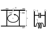
- FIG. 1 is an explanatory diagram for explaining the basic principle of a reflectarray. As shown in the figure, it is assumed that the phase of the reflected wave by each of the plurality of elements aligned on the ground plane gradually changes between adjacent elements. In the case of the illustrated example, the phase difference of the reflected wave by each adjacent element is 90 degrees. Since radio waves travel in a direction perpendicular to the equiphase surface (shown by broken lines), a reflective array is formed by arranging elements two-dimensionally while appropriately adjusting the reflection phase from each element. Thus, the incident wave can be reflected in a desired direction.
- Fig. 2 shows a mushroom structure that can be used as an element for a reflectarray.
- the mushroom structure includes a ground plate 151, a via 152, and a patch 153.
- the ground plate 151 is a conductor that supplies a common potential to a large number of mushroom structures.
- ⁇ x and ⁇ y indicate an interval in the x-axis direction and an interval in the y-axis direction between vias in adjacent mushroom structures, respectively.
- ⁇ x and ⁇ y represent the size of the ground plate 151 corresponding to one mushroom structure.
- the ground plate 151 is as large as an array of many mushroom structures.
- the via 152 is provided to electrically short-circuit the ground plate 151 and the patch 153.
- the patch 153 has a length of Wx in the x-axis direction and a length of Wy in the y-axis direction.
- the patch 153 is provided in parallel to the ground plate 151 at a distance t, and is short-circuited to the ground plate 151 through the via 152.
- t For simplicity of illustration, only two mushroom structures are shown in FIG. 2, but the reflect array has a large number of such mushroom structures in the x-axis and y-axis directions.
- each element constituting the reflect array has a mushroom structure.
- the reflect array may be formed of any element that reflects radio waves.
- a ring-shaped conductive pattern (Fig. 3 (1)), a cross-shaped conductive pattern (Fig. 3 (2)), and a plurality of parallel conductive patterns (Fig. 3 (3 )) Etc.
- a structure (FIG. 3 (4)) without a via connecting the patch and the ground plate may be used.
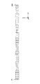
- FIG. 4 shows an enlarged plan view of the reflect array as shown in FIG. Four patches 153 arranged in a line along the line p and four patches 143 arranged along the line q adjacent to the line are shown. The number of patches is arbitrary.
- FIG. 5 shows a state in which a number of elements as shown in FIGS. 2 and 4 are aligned on the xy plane to form a reflectarray.
- Fig. 6 shows the equivalent circuit of the mushroom structure shown in Fig. 2, Fig. 4 and Fig. 5.
- Capacitance C is generated due to a gap between the mushroom-structured patch 153 aligned along the line p in FIG. 4 and the mushroom-structured patch 153 aligned along the line q.
- an inductance L is generated due to the mushroom structure vias 152 arranged along the line p and the mushroom structure vias 152 arranged along the line q. Therefore, the equivalent circuit of the adjacent mushroom structure is a circuit as shown on the right side of FIG. That is, in the equivalent circuit, the inductance L and the capacitance C are connected in parallel.
- Capacitance C, inductance L, surface impedance Zs, and reflection coefficient ⁇ can be expressed as follows.
- Equation (1) ⁇ 0 represents the dielectric constant of vacuum, and ⁇ r represents the relative dielectric constant of the material interposed between the patches.
- the element interval is the via interval ⁇ y in the y-axis direction.
- the gap g y is a gap between adjacent patches.
- g y ⁇ y ⁇ Wy.
- Wy represents the length of the patch in the y-axis direction. That is, the argument of the arccosh function represents the ratio between the element spacing and the gap.
- ⁇ represents the magnetic permeability of the material interposed between the vias
- t represents the height of the patch 153 (distance from the ground plate 151 to the patch 153).
- ⁇ represents an angular frequency
- j represents an imaginary unit.
- Equation (4) ⁇ represents free space impedance, and ⁇ represents a phase difference.
- FIG. 7 shows the relationship between the size Wy of the mushroom structure patch as shown in FIGS. 2, 4 and 5 and the reflection phase.
- the reflection phase of the mushroom structure becomes zero at a certain resonance frequency.
- the capacitance C and / or inductance L of the element it is possible to adjust the reflection phase when the element reflects the radio wave of the resonance frequency.
- the design of the reflect array it is necessary to appropriately set the reflection phase of each element by the capacitance C and / or the inductance L so that the radio wave of the resonance frequency is reflected in a desired direction.
- solid lines indicate theoretical values, and those plotted with circles indicate simulation values by finite element method analysis.
- t02 represents a graph when the distance t is 0.2 mm.
- t08 represents a graph when the distance t is 0.8 mm.
- t16 represents a graph when the distance t is 1.6 mm.
- t24 represents a graph when the distance t is 2.4 mm.
- the via spacing or element spacing ⁇ x and ⁇ y is 2.4 mm as an example.
- the reflection phase can be around 175 degrees by setting the thickness to 0.2 mm. However, even if the patch size Wy changes from 0.5 mm to 2.3 mm, the difference in the reflection phase becomes 1 degree or less, and the value of the reflection phase hardly changes. From the graph t08, the phase can be around 160 degrees by setting the thickness to 0.8 mm. At this time, when the patch size Wy changes from 0.5 mm to 2.3 mm, the reflection phase changes from about 162 degrees to 148 degrees, but the change range is as small as 14 degrees.
- the phase is 145 degrees or less, and when the patch size Wy changes from 0.5 mm to 2.1 mm, the reflection phase decreases only slowly from 144 degrees to 107 degrees.
- the reflection phase decreases rapidly.
- the reflection phase is 54 degrees for the simulation value (circle) and 0 degree for the theoretical value (solid line). Reach.
- the patch size Wx in the x-axis direction is the same for all elements, and the patch size Wy in the y-axis direction varies depending on the location of the element. .
- only the patch size Wy in the y-axis direction needs to be determined according to the location of the element, simplifying the design. become.
- one of the various via heights or substrate thicknesses t to be used in the design (e.g., t24) is selected, and the size of each of the multiple patches to be aligned is required at the position of the patch. It is determined according to the reflection phase. For example, when t24 is selected and the required reflection phase is 72 degrees at a certain patch position, the patch size Wy is about 2 mm. Similarly, the sizes of other patches are determined. Ideally, it is preferable that the patch size is designed so that the change of the reflection phase by the entire element group aligned in the reflect array is 360 degrees.
- the reflected wave is in the direction in which the reflection phase changes in the zx plane, that is, the y-axis Tilt in a direction perpendicular to or transverse to the direction (x-axis direction).
- Controlling the reflected wave in this way is referred to as “horizontal control” for convenience.
- the present invention is not limited to horizontal control.
- a reflect array is configured with the structure shown in FIG.
- the patch size and gap can be determined by several methods.
- the element spacing ⁇ x may be common and the individual patches may be asymmetric as shown in FIG. 9, or the individual patches may be symmetric and the element spacing may be different as shown in FIG.
- the element spacing ⁇ x may be common and individual patches may be designed symmetrically.
- the gap g x in the x-axis direction strongly affects the reflected wave when the radio wave having the electric field component in the x-axis direction is reflected in the desired direction.
- the radio wave having an electric field component in the x-axis direction is a TE wave (Transverse Electric wave) or a horizontal Polarization.
- horizontal polarization is a radio wave having an electric field component parallel to the incident surface or the ground (xy plane).
- the radio wave When a radio wave having an electric field component in the y-axis direction enters the reflect array for horizontal control as shown in FIGS. 4 and 5, for example, along the z-axis, the radio wave is reflected at a desired reflection angle on the zx plane.
- the reflection phase of the element is determined by the capacitance C and inductance L of the element, and in particular, the capacitance C is determined by the gap or gap between the patches.
- the gap g y in the y-axis direction is set to various values according to various reflection phase values, and the gap g x in the x-axis direction is kept constant. ing.
- the gap g y in the y-axis direction has a strong influence on the reflected wave.
- the radio wave having an electric field component in the y-axis direction is a TM wave (Transverse Magnetic wave) or a vertical wave.
- Polarization “Vertical polarization” in this case is a radio wave having an electric field component perpendicular to the incident surface or the ground (xy plane).
- the gap g x in the x-axis direction is designed so that the TE wave reflects in the desired direction
- the TM wave It can be seen that the gap g y in the y-axis direction should be designed so that is reflected in the desired direction.
- the desired direction of the TE wave and the desired direction of the TM wave may be the same or different.
- the frequencies of the TE wave and TM wave may be the same or different. The case where the frequencies of the TE wave and TM wave are different will be described later in ⁇ 3. This will be described in “Multi-band shared polarization>”.
- FIG. 13 shows an element array for one cycle of a reflect array that reflects TE waves and TM waves in the same direction.
- a plurality of element rows for one cycle shown in the figure are arranged in the x-axis and y-axis directions.
- FIG. 14 is a plan view of two element rows arranged in the y-axis direction in the reflect array in which many element rows for one period shown in FIG. 13 are arranged.
- FIG. 15 shows the values of various parameters for each of the ten elements shown in FIGS. Specifically, the dimension of the gap g y in the y-axis direction, the reflection phase corresponding to the gap g y (that is, the reflection phase for TM waves), the dimension of the gap g x in the x-axis direction, and the gap g x Specific numerical values of the reflected phase (that is, the reflected phase with respect to the TE wave), the patch size Wy in the y-axis direction, and the patch size Wx in the x-axis direction are shown.
- the phase difference of the reflected wave by each adjacent element is 36 degrees (2 ⁇ / 10 radians).
- the difference in reflection phase by each adjacent element is a divisor that is an integral multiple of 360 (for example, 36 degrees).
- the reflection phase difference it is not essential that the reflection phase difference exactly matches a divisor that is an integral multiple of 360. It is only necessary that the reflection phase difference substantially matches.
- 27 is not strictly a divisor of 360, but by arranging 13 elements while changing the reflection phase difference by 27 degrees, the range of the reflection phase of 360 degrees can be substantially covered.
- a reflection phase difference such as 27 degrees may be used.
- FIG. 16A shows a simulation result regarding the reflect array including the element arrays shown in FIG. 13-15.
- ⁇ i and ⁇ r are declinations made by the incident wave and the reflected wave with respect to the z axis
- ⁇ i and ⁇ r are made by the incident wave and the reflected wave with respect to the x axis. Declination.
- E ⁇ represents the electric field component in the ⁇ direction of the reflected radio wave
- E ⁇ represents the electric field component in the ⁇ direction of the reflected radio wave.
- the number of elements for one period for reflecting the TE wave in the desired direction and the number of elements for one period for reflecting the TM wave in the desired direction are both ten.
- the number of elements N TE for one period for reflecting the TE wave may be different from the number of elements N TM for one period for reflecting the TM wave.
- the number of elements N TE for one cycle for reflecting TE wave is 10
- element number N TM of one cycle for reflecting TM waves may be 20.
- the phase difference between the reflected waves by the adjacent elements is 36 degrees (360 ⁇ 10) for the TE wave and 18 degrees (360 ⁇ 20) for the TM wave.
- the TE wave and the TM wave are made in the same direction. Or it can reflect as intended in different directions.
- the x-axis direction and the y-axis direction are only relative directions when defining a two-dimensional plane.
- the reflect array is in the xy plane.
- the TE wave has an electric field component that changes in the x-axis direction
- the TM wave has an electric field component that changes in the y-axis and z-axis directions. Therefore, the reflect array can be created by designing the gap g x in the x-axis direction to reflect the TE wave and designing the gap g y in the y-axis direction to reflect the TM wave. This is the same as the above example. However, in the example shown in FIG.
- the TE wave has an electric field component that changes in the y-axis direction
- the TM wave has an electric field component that changes in the x-axis and z-axis directions.
- the reflected wave of the TE wave is greatly affected by the gap g y in the y-axis direction
- the reflected wave of the TM wave is greatly affected by the gap g x in the x-axis direction. Therefore, in the example shown in FIG.
- ⁇ r indicates the relative dielectric constant of the dielectric substrate interposed between the patch and the ground plane.
- c indicates the speed of light.
- the plasma frequency f p satisfies the following relationship with the plasma wave number k p .
- ⁇ ZZ indicates the effective dielectric constant of the metal medium along the via, and is represented by the following formula (10).
- epsilon h represents the relative dielectric constant of the substrate constituting the mushroom
- eta 0 indicates the impedance of free space.
- k 0 indicates the wave number of the free space
- k indicates the wave number of the mushroom medium, and is expressed by the following formula (11).
- k z represents the z component of the wave vector (wave vector), and is represented by the following formula (12).
- Equation (5) Z g represents surface impedance and satisfies the relationship of the following equation.
- ⁇ eff represents an effective impedance expressed by the following formula (14), and ⁇ is a grid parameter expressed by the following formula (15).
- FIG. 18 shows the reflection phase of a reflected wave as a function of frequency when a TE wave and a TM wave are incident on a reflect array in which elements are aligned at equal intervals in the x-axis direction and the y-axis direction.
- the relative dielectric constant ⁇ r of the substrate is 4.5
- the via height (that is, the distance between the ground plane and the patch) t is 1.52 mm
- the element spacing ⁇ x in the x-axis direction is 4.1 mm.
- the element spacing ⁇ y in the y-axis direction is also 4.1 mm.
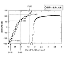
- the reflection phase gradually decreases from 150 degrees when the frequency increases from 5 GHz, the reflection phase becomes 0 when the frequency is 9 GHz (f M ), and the frequency As the value increases, the reflection phase decreases.
- the reflection phase decreases rapidly from 150 degrees when the frequency increases from 5 GHz, the reflection phase becomes 0 when the frequency is 8.25 GHz (f L ), and the reflection phase increases as the frequency increases.
- the frequency decreases and the frequency exceeds 10 GHz
- the reflection phase reaches about -180 degrees.
- the reflection phase becomes +180 degrees, and decreases rapidly.
- the reflection phase becomes 0, and as the frequency further increases, the reflection phase decreases.
- a TM wave there are two frequencies (f L , f H ) at which the reflection phase is 0 degrees.
- Such a decrease is referred to as bi-resonance or spurious resonance.
- the reflection phase of the mushroom structure (element) becomes 0 at the resonance frequency, and by adjusting the capacitance C and / or the inductance L of the plurality of elements constituting the reflect array, the radio wave of the resonance frequency is generated. It can be reflected in a desired direction.
- the gap g x in the x-axis direction is designed to appropriately reflect the TE wave of the first frequency
- the gap g y in the y-axis direction is designed to appropriately reflect the TM wave of the second frequency.
- the gap g x in the x-axis direction strongly influences the reflected wave, while the y-axis
- the gap g y in the y-axis direction has a dominant influence on the reflected wave. This is the same in the case of multiband.
- FIG. 19 shows the relationship between the gap size g y in the y-axis direction and the reflection phase of an element having a mushroom structure.
- the radio wave is a TM wave
- the incident angle ⁇ i is 20 degrees.
- the shape of the graph shown is merely an example, and other values are used when other parameter values are used.
- FIG. 20 shows the relationship between the gap size g x in the x-axis direction and the reflection phase of a mushroom structure element.
- the radio wave is a TE wave
- the incident angle ⁇ i is 20 degrees.
- the shape of the illustrated graph is merely an example, and other shapes are used when other parameter values are used.
- the gap g x in the x-axis direction is designed to appropriately reflect the TE wave of the first frequency f L , and the TM wave of the second frequency f H is appropriately reflected. It is necessary to design the gap g y in the y-axis direction.
- the reflection phase to be realized with respect to the TM wave by a certain element is determined, and the value of the gap size g y in the y-axis direction corresponding to the reflection phase is obtained in the graph shown in FIG.
- the gap size g x in the x-axis direction and the reflection phase are determined using a graph when the gap size in the y-axis direction is g y .
- the gap sizes g x and g y of individual elements can be determined. For example, FIG.
- the gap size g y in the y-axis direction is 0.15 mm.
- the gap size g x in the x-axis direction and the reflection phase are determined using a graph when the gap size g y in the y-axis direction is 0.15 mm.
- the gap size g y in the y-axis direction is 0.89 mm.
- the gap size g x in the x-axis direction and the reflection phase are determined using a graph when the gap size g y in the y-axis direction is 0.89 mm.
- the gap size g y in the y-axis direction is 1.62 mm.
- the gap size g x in the x-axis direction and the reflection phase are determined using a graph when the gap size g y in the y-axis direction is 1.62 mm.
- the method of determining the gap sizes g x , g y and the reflection phase is merely an example, and the gap sizes g x , g y and the reflection phase may be determined by any appropriate method.
- ⁇ 3.2 Period boundary Configure the reflect array by changing the gap size g x and g y between the element patches along the x-axis direction and gradually changing the reflection phase of the TE and TM waves along the x-axis direction. In this case, it is difficult to change the reflection phase also in the y-axis direction. Therefore, it is desirable that the element array for one period constituting the reflect array is formed by a plurality of elements arranged in a line in the x-axis direction, and the reflect array is formed by positioning a large number of the element arrays. By setting the periodic boundaries in the element rows in this way, the design of the reflect array can be greatly simplified.
- the incident direction and the reflection direction of radio waves are set as shown in FIG. 17A.
- the origin corresponds to one element in the reflectarray.
- the incident unit vector u i along the direction in which the incident wave travels can be written as follows.
- Reflecting unit vector u r along the direction in which the reflected wave travels can be written as follows.
- the center coordinates of each of the plurality of elements constituting the reflect array are (m ⁇ x, n ⁇ y, 0).
- N x is the maximum value of m
- N y is the maximum value of n.
- the position vector r mn of the mth element in the x-axis direction and the nth element in the y-axis direction (referred to as the mnth element for convenience) can be written as follows.
- r mn (m ⁇ x, n ⁇ y, 0) (19)
- the reflection phase ⁇ mn (f) to be realized by the mn-th element can be written as follows.
- ⁇ mn (f) (2 ⁇ f / c) (r mn ⁇ u i ⁇ r mn ⁇ u r ) + 2 ⁇ N (20)
- “ ⁇ ” represents an inner product of vectors.
- 2 ⁇ N 0, generality is not lost.
- ⁇ mn (f) can be set to an arbitrary value by Equation (21).
- the difference in reflection phase ( ⁇ mn (f) - ⁇ m-1n ( It is preferable that f) or ⁇ mn (f) - ⁇ mn-1 (f)) is a divisor (eg, 36 degrees) that is an integral multiple of 360.
- the reflection phase ⁇ mn (f) to be realized by the mn-th element generally depends on ⁇ x and ⁇ y. However, in Equation (21), if, when that is multiplied by ⁇ y (sin ⁇ i sin ⁇ i -sin ⁇ r sin ⁇ r) was equal to identically 0, the reflection phase alpha mn (f) is independent of the [Delta] y No longer. In this case, the reflection phase ⁇ mn (f) gradually changes in the x-axis direction, but can be made constant in the y-axis direction. In this way, the reflection array to be realized by each element changes in the x-axis direction but is constant in the y-axis direction, so that the reflect array can be easily realized.
- the deflection angle ⁇ r of the reflected wave from the z-axis can be uniquely determined based on the deflection angle ⁇ r of the reflected wave from the x-axis.
- Equation (25) or Equation (27) the TE wave and TM wave reflection phases gradually change along the x-axis direction, but along the y-axis direction. It is possible to prevent the reflection phase from changing.
- the element array for one cycle that composes the reflect array can be formed by a plurality of elements arranged in a line in the x-axis direction. By setting such a periodic boundary, the design of the reflect array is greatly simplified.
- the reflection phase ⁇ mn (f) of the mn-th element depends on the frequency f (specifically, ⁇ mn (f) ⁇ f) . Therefore, in general, the reflection phase ⁇ mn (f L ) of the element at the first frequency f L and the reflection phase ⁇ mn (f H ) of the element at the second frequency f H are not the same. Therefore, generally speaking, the direction in which the TE wave of the first frequency f L is reflected by the reflect array and the direction in which the TM wave of the second frequency f H is reflected by the reflect array are controlled independently.
- the reflection phase difference ⁇ x (f L ) for the TE wave of the first frequency f L and the reflection phase difference ⁇ x (f H ) for the TM wave of the second frequency f H are the incidence of the TE wave and the TM wave.
- the direction ( ⁇ i , ⁇ i ) and the desired direction ( ⁇ r , ⁇ r ) are common, they can be written as follows.
- Equation (29) (2 ⁇ f L / c) ⁇ x (sin ⁇ i cos ⁇ i ⁇ sin ⁇ r cos ⁇ r ) (29)
- ⁇ x (f H ) (2 ⁇ f H / c) ⁇ x (sin ⁇ i cos ⁇ i ⁇ sin ⁇ r cos ⁇ r )
- ⁇ x (f L ): ⁇ x (f H ) f L : f H (31) That is, the ratio of the reflection phase difference ⁇ x (f L ) for the TE wave of the first frequency f L and the reflection phase difference ⁇ x (f H ) for the TM wave of the second frequency f H is the first frequency f When equal to the ratio of L and the second frequency f H , the TE wave and the TM wave can be reflected in a common desired direction ( ⁇ r , ⁇ r ).
- the reflection phase difference is 36 degrees
- the reflection phase difference is 27.3 degrees
- 40 elements arranged in a line in the x-axis direction form one period of the reflectarray, and 13 elements for reflecting TE waves are included in one period.
- ten elements for reflecting TM waves can be included for four periods.
- FIG. 22 shows a plan view of an element row for one period of such 40 elements.
- a reflect array can be formed.
- FIG. 23 shows values of various parameters for each of the 40 elements shown in FIG. Specifically, phase for TM wave, dimension of gap g y in y-axis direction, phase for TE wave, dimension of gap g x in x- axis direction, patch size Wy in y-axis direction and patch size Wx in x-axis direction Specific numerical values of are shown.
- the phase difference of the reflected wave by each adjacent element is 36 degrees for the TM wave and 27 degrees for the TE wave.
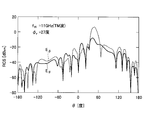
- FIG. 24 is a simulation result showing a radar cross section (RCS) (dB sm ) for a reflect array including a number of element arrays for one period shown in FIGS. 22 and 23.
- the incident and reflected radio waves are 8.25 GHz TE waves.
- the horizontal axis of the graph represents the deviation angle ⁇ from the z axis.
- E ⁇ represents the electric field component in the ⁇ direction of the reflected wave
- E ⁇ represents the electric field component in the ⁇ direction of the reflected wave.
- Equation (22) the reflection phase ⁇ mn (f) to be realized by the element gradually changes in the x-axis direction. However, it is made constant in the y-axis direction. However, the embodiment is not limited to this example, and conversely, the reflection phase ⁇ mn (f) to be realized by the element gradually changes in the y-axis direction but is constant in the x-axis direction. You can also. In that case, in equation (21), the coefficient of ⁇ x (sin ⁇ i cos ⁇ i ⁇ sin ⁇ r cos ⁇ r ) needs to be equal to zero. In this case, the following equation is established.
- the deflection angle ⁇ r of the reflected wave from the z-axis can be uniquely determined from the deflection angle ⁇ r of the reflected wave from the x-axis.
- the reflection phase ⁇ mn (f) to be realized by the mn-th element can be written as follows.
- the difference ⁇ y (f) with respect to the reflection phase ⁇ mn-1 (f) can be written as follows using Equation (21).
- the ratio of the reflection phase difference ⁇ y (f L ) for the TE wave of the first frequency f L and the reflection phase difference ⁇ y (f H ) for the TM wave of the second frequency f H is the first frequency f
- the TE wave and the TM wave can be reflected in a common desired direction ( ⁇ r , ⁇ r ).
- the reflection phase by an arbitrary element (mn) among the plurality of elements constituting the reflect array is expressed by the first axis (
- the reflection phase of the element adjacent to the mn-th element in the (x-axis or y-axis) direction differs from the reflection phase by a predetermined value, but is equal to the reflection phase of the element adjacent to the element in the second axis (y-axis or x-axis) direction It can be said.
- the magnitude of the second axial component of the incident unit vector u i is equal to the magnitude of the second axial component of the reflected unit vector u r, and can be said.
- the ratio of the reflection phase difference ⁇ x or y (f L ) for the TE wave of the first frequency f L and the reflection phase difference ⁇ x or y (f H ) for the TM wave of the second frequency f H is When the ratio is equal to the ratio between the frequency f L of 1 and the second frequency f H , the TE wave and the TM wave can be reflected in a common desired direction ( ⁇ r , ⁇ r ).
- FIG. 28 shows an explanatory diagram for explaining the basic principle of the reflectarray.
- the phase of the reflected wave by each of the plurality of elements aligned on the ground plane gradually changes between adjacent elements.
- the phase difference of the reflected wave by each adjacent element is 90 degrees. Since radio waves travel in a direction perpendicular to the equiphase surface (shown by the broken line), a reflective array is formed by arranging the elements on a plane while appropriately adjusting the reflection phase from each element. The incident wave can be reflected in a desired direction.
- the phase ⁇ mn given to the mn-th element in the design of the reflect array configured by the M ⁇ N array is expressed by the equation (40) using the position vector r mn and the incident and reflection direction unit vectors u i and ur. (Non-Patent Document 2).
- (40) as in equation when participate the reflection phase of alpha mn to mn th element a plane perpendicular to the unit vector u r of the reflecting direction becomes equiphase surface, the reflected wave in the direction of u r Advances.
- k f is a wave number at the operating frequency f and is represented by the equation (41).
- Equation (42) the phase difference between the mn-th and (m ⁇ 1) n-th elements adjacent in the x direction is Equation (42), and the phase difference between the elements adjacent in the y direction is Equation (43). Given.
- phase difference between the mn-th and m (n ⁇ 1) -th elements adjacent in the y direction is given by equation (42), and the phase difference between the elements adjacent in the y direction is given by expression (43).
- the unit vector u i can circle the incident direction and the unit vector u r can circle reflection direction of the plane formed is obtained as a plane formed by the two straight lines. This is called a reflective surface.
- the electric field is orthogonal to the reflecting surface, it is called a TE wave, and when it is parallel, it is called a TM wave.
- phase difference with respect to TE incidence is ⁇ mxTE and ⁇ nyTE TM
- the phase difference with respect to ⁇ mxTE and ⁇ nyTM is set to ⁇ mxTM , ⁇ nyTM
- the formulas (44) and (45) hold both the TE wave and TM wave It can be seen that the incident wave can be reflected in the same direction from the direction.
- equations (46) and (47) may be modified to make the phase ratio and the wave number ratio equal. At this time, if the phase ratio is the same from the equations (42) and (43), the phase difference ratio is also equal. That is, equation (48) may be established.
- Equation (48) indicates that both the phase difference ratio in the Y direction and the phase difference ratio in the X direction are frequency ratios.
- Equation (49) in order to reflect each in the same direction when the first frequency is TM incident and the second frequency is TM incident, Equation (49) may be established.
- equation (50) may be established.
- equation (51) In order to reflect each in the same direction when the first frequency is TE incident and the second frequency is TM incident, equation (51) may be established.
- the equation (52) may be established.
- the TE incidence It can be seen that the ratio of the phase obtained at the first frequency at this time, the ratio of the phase obtained at the second frequency at the time of TM incidence, and the ratio of wave numbers should be equal.
- FIG. 29 shows an equivalent circuit of a mushroom structure.
- Capacitance C occurs due to the gap between the patches 253 of the mushroom structure in FIG. Therefore, when the mushroom structure patches 253 arranged along the line p in FIG. 29 and the mushroom structure patches arranged along the line q are arranged in the mushrooms having different gap sizes, the capacitances C1,. Will line up along line q.
- an inductance L is generated due to the mushroom structure via 252 aligned along the line p and the mushroom structure via 252 aligned along the line q. Therefore, the equivalent circuit of the adjacent mushroom structure is a circuit as shown on the right side of FIG. That is, in the equivalent circuit, the inductance L and the capacitance C are connected in parallel. Capacitance C is expressed by equations (53) and (54).
- Equation (53) is a capacitance generated when the electric field is parallel to the x direction
- Equation (54) is a capacitance generated when the electric field is parallel to the y direction.
- the capacitance of the mushroom structure can be changed by changing the value of the gap.
- the patch size in the x direction changes, which affects the capacitance in the y direction. That is, there arises a problem that the capacitance value cannot be determined independently in the x and y directions.
- Equations (53) and (54) ⁇ 0 represents the dielectric constant of the vacuum, and ⁇ r represents the relative dielectric constant of the material interposed between the patches.
- the element interval is the via interval ⁇ y in the y-axis direction.
- the gap g y is a gap between adjacent patches.
- g y ⁇ y ⁇ Wy.
- Wy represents the length of the patch in the y-axis direction. That is, the argument of the arccosh function represents the ratio between the element spacing and the gap.
- the inductance L, the surface impedance Zs, and the reflection coefficient ⁇ are expressed by the equations (55), (56), and (57), respectively.
- Equations (53) and (54) ⁇ 0 represents the dielectric constant of the vacuum, and ⁇ r represents the relative dielectric constant of the material interposed between the patches.
- Wy represents the length of the patch in the y-axis direction, and Wx represents the length of the patch in the x-axis direction. That is, the argument of the arccosh function represents the ratio between the element spacing and the gap.
- ⁇ represents the magnetic permeability of the material interposed between the vias
- t represents the height of the patch 253 (the distance from the ground plate 251 to the patch 253).
- ⁇ represents an angular frequency
- j represents an imaginary unit.
- Equation (57) ⁇ represents free space impedance, and ⁇ represents a phase difference.
- the reflection phase of the mushroom structure becomes 0 at a certain resonance frequency. Since the resonance frequency is shifted by adjusting the capacitance C and / or the inductance L of the element, the value of the reflection phase can be adjusted.
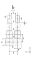
- FIG. 31A and 31B are diagrams illustrating the structure of an H-type mushroom element according to an embodiment of the present invention.
- an H-type mushroom element according to an embodiment of the present invention includes a ground plate 251, a via 252, and an H-type patch 254.
- each H-type mushroom element has a via 252 and an H-type patch 254, and a plurality of H-type mushroom elements are arranged on the ground plate 251 in an array.
- the H-type patch 254 is composed of three rectangular parts, two rectangular outer patches of the same size and one rectangular inner patch, and the H-type patch 254 is defined by one side of the rectangle.
- the two outer patches are connected to the inner patch so as to sandwich the inner patch so as to be symmetric with respect to the first direction (X direction) and the second direction (Y direction) orthogonal to the first direction.
- the length of the outer patch in the X direction is Ox
- the length of the H-type patch in the Y direction is Oy
- the length of the inner patch in the X direction is Ix
- the inner patch The length in the Y direction of the patch is Iy.
- the H-shaped patch has an H-shaped shape as shown in FIGS. 31 and 32.
- the H-shaped patch according to the present invention is not limited to this, for example, two outer patches. May have different sizes.
- the H-type patch may be asymmetric with respect to the first direction and the second direction. Further, the first direction and the second direction described above do not necessarily have to be orthogonal.
- the H-type patch 254 is composed of three rectangular portions of two rectangular outer patches of the same size and one rectangular inner patch, and the H-type patch is defined by one side of the rectangle.
- the patch is an arbitrary shape in which two outer patches are connected to the inner patch so as to sandwich the inner patch so as to be symmetric with respect to one direction and a second direction orthogonal to the first direction.
- the patches of the reflecting elements shown in FIGS. 33 to 37 have shapes defined in this way, and are all H-type patches.
- Ox> Ix In a typical H-type patch, Ox> Ix.
- the present invention is not limited to this, and Ox ⁇ Ix may be satisfied.
- the reflect array according to each embodiment of the present invention is configured by arranging a plurality of H-type mushroom elements having the above-described H-type patch in an array.
- the length of Oy is changed for the incidence of an electric field parallel to the Y direction, and the length of Ox is constant for the incidence of an electric field parallel to the X direction.
- the H-type mushroom element is arranged so as to change only the value of Ix. If Ox is considered to correspond to the area of the capacitor forming the capacitance (capacitance) in the X direction, that is, Wx in the equation (53), the value of Ox does not change even if Ix is changed.
- the second By changing the value of the gap between the inner patches generated between the inner patches in the direction, the reflection phase with respect to the polarization in the second direction can be changed.
- the capacitance generated between the H-type elements adjacent in the first direction is determined based on the size of the cap between the first outer patches
- the capacitance generated between the H-type elements adjacent in the second direction is It will be determined based on the size of the gap between the second outer patches.
- the H-shaped patch is composed of the four outer vertices of the H-shaped patch composed of two rectangular outer patches and the inner four vertices composed of the inner patches, and is incident in parallel to the first direction.
- the length of the inner patch in the first direction determined by the position of the four vertices of the inner patch is maintained while maintaining the position of the four vertices of the outer patch and the size of the outer patch constant. It is determined. Further, in order to change the reflection phase of the electric field incident in parallel with the second direction, the length in the second direction determined by the positions of the four vertices of the outer patch of the H-type patch in the second direction is determined.
- FIG. 38 is a diagram showing the relationship between the reflection phase and the length of the outer patch in the first embodiment of the present invention.
- the simulation results regarding the relationship between the reflection phase of the electric field incident in parallel to the Y direction and Oy are shown for three bands of 8.25 GHz, 11 GHz, and 14.3 GHz.
- FIG. 39 is a diagram showing the relationship between the reflection phase and the length of the inner patch in the first embodiment of the present invention.
- the outer patch length Oy in the Y direction is 2.8 mm and 3.9 mm
- the simulation result regarding the relationship between the reflection phase of the electric field incident in parallel to the X direction and Iy is shown.
- the value of Iy is also determined.
- the value of the reflection phase can be changed by nearly 360 degrees by changing Ix.
- the reflection phase of TE (Transverse Electric wave) incidence can be changed independently of the reflection phase of TM (Transverse Magnetic wave) incidence.
- Table 1 in FIG. 40 shows design values of the reflect array using the H-type mushroom element according to the first embodiment of the present invention.
- the values of Oy and Ix were determined so as to satisfy Table 1 from FIGS.
- FIG. 41 shows the selected value of Oy
- FIG. 42 shows the selected value of Ix.
- FIG. 33 is an overall view of the reflect array using the H-type mushroom element according to the first embodiment of the present invention, whose structure is determined from FIGS. 38 and 39 so that the reflection phase can be obtained based on the design values shown in Table 1. is there.
- FIGS. 34 to 37 are enlarged views of the reflect array using the H-type mushroom element.
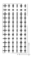
- the multiband reflectarray according to the first embodiment is configured by arranging H-type mushroom elements of various sizes in an array.
- FIGS. 34 to 37 an enlarged view of each part of the multiband reflectarray shown in FIG. 33 is shown.
- a total of 30 H-type mushroom elements, 3 in the X direction and 10 in the Y direction, are arranged in an array, with different Oy 1 -Oy 10 and Ix 1 -Ix 10
- a set 211 of 10 H-type mushroom elements having a size and the same Ox size are arranged in the Y direction.
- Similar array sets 212 and 213 of H-type mushroom elements are arranged in the X direction.
- a total of 30 H-type mushroom elements, 3 in the X direction and 10 in the Y direction, are arranged in an array, and different Oy 11 ⁇
- a set 221 of ten H-type mushroom elements having the size of Oy 20 and Ix 11 -Ix 20 and the same size of Ox is arranged in the Y direction.
- Similar array sets 222, 223 of H-type mushroom elements are arranged in the X direction.
- a total of 30 H-type mushroom elements, 3 in the X direction and 10 in the Y direction, are arranged in an array, and different Oy 21 ⁇
- a set 231 of ten H-type mushroom elements having the sizes of Oy 30 and Ix 21 -Ix 30 and the same size of Ox is arranged in the Y direction.
- Similar array sets 232 and 233 of H-type mushroom elements are arranged in the X direction.
- a total of 30 H-type mushroom elements, 3 in the X direction and 10 in the Y direction, are arranged in an array, and different Oy 31 ⁇
- a set 241 of ten H-type mushroom elements having the size of Oy 40 and Ix 31 -Ix 40 and the same size of Ox is arranged in the Y direction.
- Similar array sets 242 and 243 of H-type mushroom elements are arranged in the X direction.
- FIG. 43 and 44 show the scattering cross sections when the light enters the reflect array under the design conditions shown in Table 1.
- FIG. 45 is an enlarged view of a reflect array using an H-type mushroom element according to the second embodiment of the present invention.
- the size of Iy is variable, but as shown in FIG. 45, in the multiband reflectarray according to the second embodiment, Iy is set to a constant size.
- FIG. 46 is a diagram showing a change with respect to Oy of the reflection phase characteristic of the multiband reflectarray by the TE incident H type mushroom element according to the second embodiment of the present invention.
- Oy when Oy is changed while Iy is kept constant, even if the length of Ix is changed to 2 mm and 3.7 mm, a simulation result is obtained in which the value of the reflection phase shows a substantially similar curve. It has been. That is, it can be understood that the reflection phase can be determined by the length of Oy with respect to the incidence of the electric field parallel to the Y direction without depending on the length of Ix.
- FIG. 47 is a diagram showing a change with respect to Ix of the reflection phase characteristic of the multiband reflectarray by the TM incident H type mushroom element according to the second embodiment of the present invention.
- Ix is changed while Ox is kept constant, even if the length of Oy is changed to 3 mm and 3.7 mm, a simulation result is obtained in which the value of the reflection phase shows a substantially similar curve. It has been. That is, for the incidence of an electric field parallel to the X direction, the reflection phase can be determined by the length of Ix without depending on the length of Oy.
- FIG. 48 is an enlarged view of a reflect array using an H-type mushroom element according to the third embodiment of the present invention.
- the multiband reflectarray according to the third embodiment for the incidence of an electric field parallel to the X direction, the length of Ix is changed while the length of Ox is kept constant, and the incidence of the electric field parallel to the Y direction is performed.
- the H-type mushroom element is arranged to change the length of Oy while keeping the length of Iy constant. That is, each H-type mushroom element has the same size of Ox and Iy and different sizes of Ix and Oy.
- each H-type mushroom element has the same Ox, different Oy and Ix, and the same Iy. This makes it possible to change the reflection phase of TE incidence independently of the reflection phase of TM incidence, as in the first embodiment, and the electric field incident parallel to the X direction as described above with reference to FIG.
- the graphs showing the relationship between the reflection phase and Iy can be made to overlap each other.
Abstract
Un aspect de la présente invention porte sur un réseau réflecteur ayant une pluralité d'éléments disposés dans une forme de réseau, dans lequel chacun des éléments a une plaque en forme de H disposée éloignée d'une plaque de masse, la plaque en forme de H est configurée par quatre sommets externes de la plaque en forme de H, qui sont formés par deux plaques externes rectangulaires, et quatre sommets internes formés par une plaque interne, afin de changer la phase de réflexion d'un champ électrique incident parallèle à une première direction, la longueur de la plaque interne dans la première direction déterminée par les positions des quatre sommets de la plaque interne est déterminée pendant que les positions des quatre sommets de la plaque externe et la taille de la plaque externe sont maintenues constantes, et afin de changer la phase de réflexion d'un champ électrique incident parallèle à une seconde direction, la longueur dans la seconde direction déterminée par les positions des quatre sommets des plaques externes de la plaque en forme de H par rapport à la seconde direction est déterminée.
Priority Applications (3)
| Application Number | Priority Date | Filing Date | Title |
|---|---|---|---|
| CN201380050608.9A CN104685716B (zh) | 2012-10-01 | 2013-09-20 | 反射阵列 |
| EP13844308.0A EP2905840B1 (fr) | 2012-10-01 | 2013-09-20 | Réseau réflecteur |
| US14/428,102 US9537221B2 (en) | 2012-10-01 | 2013-09-20 | Reflectarray |
Applications Claiming Priority (4)
| Application Number | Priority Date | Filing Date | Title |
|---|---|---|---|
| JP2012-219061 | 2012-10-01 | ||
| JP2012219061A JP5469724B1 (ja) | 2012-10-01 | 2012-10-01 | リフレクトアレー |
| JP2013018926A JP5993319B2 (ja) | 2013-02-01 | 2013-02-01 | リフレクトアレー及び素子 |
| JP2013-018926 | 2013-02-01 |
Publications (1)
| Publication Number | Publication Date |
|---|---|
| WO2014054444A1 true WO2014054444A1 (fr) | 2014-04-10 |
Family
ID=50434774
Family Applications (1)
| Application Number | Title | Priority Date | Filing Date |
|---|---|---|---|
| PCT/JP2013/075527 WO2014054444A1 (fr) | 2012-10-01 | 2013-09-20 | Réseau réflecteur |
Country Status (4)
| Country | Link |
|---|---|
| US (1) | US9537221B2 (fr) |
| EP (1) | EP2905840B1 (fr) |
| CN (1) | CN104685716B (fr) |
| WO (1) | WO2014054444A1 (fr) |
Families Citing this family (9)
| Publication number | Priority date | Publication date | Assignee | Title |
|---|---|---|---|---|
| WO2014020969A1 (fr) * | 2012-07-31 | 2014-02-06 | 株式会社 エヌ・ティ・ティ・ドコモ | Réseau réfléchissant |
| US10020594B2 (en) * | 2015-10-21 | 2018-07-10 | Gwangji Institute of Science and Technology | Array antenna |
| CN107359409B (zh) * | 2017-06-22 | 2019-08-27 | 西安电子科技大学 | 一种应用于基站通信系统的双馈电宽带高增益天线 |
| JP6970051B2 (ja) * | 2018-04-05 | 2021-11-24 | 株式会社Soken | 反射低減装置 |
| US11223112B2 (en) * | 2019-03-29 | 2022-01-11 | GM Global Technology Operations LLC | Inverted microstrip travelling wave patch array antenna system |
| US11476587B2 (en) | 2019-06-14 | 2022-10-18 | City University Of Hong Kong | Dielectric reflectarray antenna and method for making the same |
| US11876298B2 (en) | 2020-11-19 | 2024-01-16 | Metawave Corporation | Active redirection devices for wireless applications |
| US11611152B2 (en) * | 2021-06-24 | 2023-03-21 | Silicon Laboratories | Metamaterial antenna array with isolated antennas |
| US11978962B2 (en) | 2022-06-22 | 2024-05-07 | Silicon Laboratories Inc. | Rotational symmetric AoX antenna array with metamaterial antennas |
Citations (4)
| Publication number | Priority date | Publication date | Assignee | Title |
|---|---|---|---|---|
| JP2007096868A (ja) * | 2005-09-29 | 2007-04-12 | Mitsubishi Electric Corp | 反射板および該反射板を備えたリフレクタアンテナ |
| JP2008252046A (ja) * | 2007-03-30 | 2008-10-16 | Fujimori Kogyo Co Ltd | 周波数選択遮蔽型の電磁波シールド積層体 |
| JP2010062689A (ja) * | 2008-09-01 | 2010-03-18 | Ntt Docomo Inc | 無線通信システム、周期構造反射板及びテーパ付きマッシュルーム構造 |
| JP2012034331A (ja) | 2010-02-26 | 2012-02-16 | Ntt Docomo Inc | マッシュルーム構造を有する装置 |
Family Cites Families (10)
| Publication number | Priority date | Publication date | Assignee | Title |
|---|---|---|---|---|
| JP3343764B2 (ja) | 1992-08-27 | 2002-11-11 | 株式会社東芝 | 携帯用無線装置及び平面アンテナ |
| US7911386B1 (en) * | 2006-05-23 | 2011-03-22 | The Regents Of The University Of California | Multi-band radiating elements with composite right/left-handed meta-material transmission line |
| WO2008050441A1 (fr) | 2006-10-26 | 2008-05-02 | Panasonic Corporation | Dispositif d'antenne |
| WO2008132785A1 (fr) * | 2007-04-12 | 2008-11-06 | Panasonic Corporation | Dispositif d'antenne |
| US7623088B2 (en) * | 2007-12-07 | 2009-11-24 | Raytheon Company | Multiple frequency reflect array |
| JP5371633B2 (ja) | 2008-09-30 | 2013-12-18 | 株式会社エヌ・ティ・ティ・ドコモ | リフレクトアレイ |
| FR2936906B1 (fr) * | 2008-10-07 | 2011-11-25 | Thales Sa | Reseau reflecteur a arrangement optimise et antenne comportant un tel reseau reflecteur |
| EP2437351A4 (fr) | 2009-05-29 | 2013-01-23 | Ntt Docomo Inc | Reflectarray |
| WO2011008558A1 (fr) * | 2009-06-29 | 2011-01-20 | Viasat, Inc. | Antenne hybride inclinée à ouverture unique |
| JP5236754B2 (ja) | 2010-02-26 | 2013-07-17 | 株式会社エヌ・ティ・ティ・ドコモ | マッシュルーム構造を有する装置 |
-
2013
- 2013-09-20 WO PCT/JP2013/075527 patent/WO2014054444A1/fr active Application Filing
- 2013-09-20 US US14/428,102 patent/US9537221B2/en active Active
- 2013-09-20 CN CN201380050608.9A patent/CN104685716B/zh active Active
- 2013-09-20 EP EP13844308.0A patent/EP2905840B1/fr active Active
Patent Citations (4)
| Publication number | Priority date | Publication date | Assignee | Title |
|---|---|---|---|---|
| JP2007096868A (ja) * | 2005-09-29 | 2007-04-12 | Mitsubishi Electric Corp | 反射板および該反射板を備えたリフレクタアンテナ |
| JP2008252046A (ja) * | 2007-03-30 | 2008-10-16 | Fujimori Kogyo Co Ltd | 周波数選択遮蔽型の電磁波シールド積層体 |
| JP2010062689A (ja) * | 2008-09-01 | 2010-03-18 | Ntt Docomo Inc | 無線通信システム、周期構造反射板及びテーパ付きマッシュルーム構造 |
| JP2012034331A (ja) | 2010-02-26 | 2012-02-16 | Ntt Docomo Inc | マッシュルーム構造を有する装置 |
Non-Patent Citations (9)
| Title |
|---|
| D. M. POZAR; T. S. TARGONSKY; H. D. SYRIGOS: "Design of millimeter wave microstrip reflectarrays", IEEE TRANS. ANTENNAS PROPAGAT., vol. 45, no. 2, 1997, pages 287 - 295 |
| FAN YANG; ANG YU; ATEF ELSHERBENI; JOHN HUANG: "Single-Layer Multi-band Circularly Polarized Reflect array Antenna: Concept, Design and Measurement", URSI GENERAL ASSEMBLY, CHICAGO, ILLINOIS, 7 August 2008 (2008-08-07) |
| J. SHEN; Y. ODA; T. FURUNO; T. MARUYAMA; T. OHYA: "VTC2011", May 2011, SPRING, article "A novel approach for capacity improvement of 2x2 MIMO in LOS channel using reflectarray" |
| L. LI; Q. CHEN; Q. YUAN; K. SAWAYA; T. MARUYAMA; T. FURUNO; S UEBAYASHI: "Frequency Selective Reflectarray using Crossed-Dipole Elements with Square Loops for Wireless Communication Applications", IEEE TRANS. ANTENNAS PROPAGAT., vol. AP-59, no. 1, 2011, pages 89 - 99 |
| PAYAM NAYERI; FAN YANG; ATEF Z. ELSHERBENI: "Single-Feed Multi-Beam Reflectarray Antennas", IEEE AP-S, 2010 |
| T. MARUYAMA; J. SHEN; N. TRAN; Y. ODA: "Multi-band Reflectarray using Mushroom Structure", IEEE ICWITS, 2012 |
| T. MARUYAMA; T. FURUNO; T. OHYA; Y. ODA; Q. CHEN; K. SAWAYA: "Dual Frequency Selective Reflectarray for Propagation Improvement", IEEE IWAT, March 2010 (2010-03-01), pages 1 - 4,5464764 |
| T. MARUYAMA; T. FURUNO; Y. ODA; J. SHEN; T. OHYA: "Capacitance value control for metamaterial reflectarray using multi-layer mushroom structure with parasitic patches", ACES JOURNAL, vol. 27, no. 1, January 2012 (2012-01-01), pages 28 - 41 |
| T. MARUYAMA; Y. ODA; J. SHEN; N. TRAN; H. KAYAMA: "Design of wide angle reflection reflectarray using multi-layer mushroom structure to improve propagation", IEEE URSI GENERAL ASSEMBLY AND SCIENTIFIC SYMPOSIUM, 2011 XXXTH URSI, August 2011 (2011-08-01) |
Also Published As
| Publication number | Publication date |
|---|---|
| US9537221B2 (en) | 2017-01-03 |
| US20150229029A1 (en) | 2015-08-13 |
| EP2905840A1 (fr) | 2015-08-12 |
| CN104685716A (zh) | 2015-06-03 |
| EP2905840A4 (fr) | 2016-05-11 |
| CN104685716B (zh) | 2017-11-17 |
| EP2905840B1 (fr) | 2018-08-01 |
Similar Documents
| Publication | Publication Date | Title |
|---|---|---|
| WO2014054444A1 (fr) | Réseau réflecteur | |
| JP6766180B2 (ja) | アンテナアレイ内の相互結合を低減するための装置および方法 | |
| US9812786B2 (en) | Metamaterial-based transmitarray for multi-beam antenna array assemblies | |
| US8319698B2 (en) | Reflector array and antenna comprising such a reflector array | |
| US20130229296A1 (en) | Multi-beam reflectarray | |
| US9620862B2 (en) | Reflectarray | |
| JP5410559B2 (ja) | リフレクトアレー及び設計方法 | |
| JP6282469B2 (ja) | アンテナ | |
| JP5410558B2 (ja) | リフレクトアレー及び設計方法 | |
| JP2012034332A (ja) | マッシュルーム構造を有する装置 | |
| JP5398858B2 (ja) | リフレクトアレー及び設計方法 | |
| JP5480855B2 (ja) | マルチビームリフレクトアレイ | |
| JP5469724B1 (ja) | リフレクトアレー | |
| JP5993319B2 (ja) | リフレクトアレー及び素子 | |
| US11502418B2 (en) | Network for forming multiple beams from a planar array | |
| JP5635567B2 (ja) | リフレクトアレー | |
| Hodgkinson et al. | Design of a Reconfigurable Phase Gradient Metasurface for Beam Steering Applications | |
| Ha et al. | Direct synthesis of dual-parameter concentric ring RA with enhanced bandwidth | |
| JP5536836B2 (ja) | 設計方法及びリフレクトアレー | |
| Yin et al. | Metasurface Lens Antenna with Deflected 1-D Flat-Top Pattern | |
| Jnana et al. | Performance analysis of polarization reconfigurable Antenna using Metasurface | |
| Carrasco et al. | Switchable-beam reflectarray with aperiodic-gathered elements based on PIN diodes | |
| JP2011066697A (ja) | アンテナ装置およびセクタアンテナ装置 |
Legal Events
| Date | Code | Title | Description |
|---|---|---|---|
| 121 | Ep: the epo has been informed by wipo that ep was designated in this application |
Ref document number: 13844308 Country of ref document: EP Kind code of ref document: A1 |
|
| WWE | Wipo information: entry into national phase |
Ref document number: 14428102 Country of ref document: US |
|
| WWE | Wipo information: entry into national phase |
Ref document number: 2013844308 Country of ref document: EP |
|
| NENP | Non-entry into the national phase |
Ref country code: DE |