WO2014041905A1 - 試験用治具、検査装置、載置装置および試験装置 - Google Patents
試験用治具、検査装置、載置装置および試験装置 Download PDFInfo
- Publication number
- WO2014041905A1 WO2014041905A1 PCT/JP2013/070318 JP2013070318W WO2014041905A1 WO 2014041905 A1 WO2014041905 A1 WO 2014041905A1 JP 2013070318 W JP2013070318 W JP 2013070318W WO 2014041905 A1 WO2014041905 A1 WO 2014041905A1
- Authority
- WO
- WIPO (PCT)
- Prior art keywords
- test
- pallet
- contact
- device under
- contact block
- Prior art date
- Legal status (The legal status is an assumption and is not a legal conclusion. Google has not performed a legal analysis and makes no representation as to the accuracy of the status listed.)
- Ceased
Links
Images












Classifications
-
- G—PHYSICS
- G01—MEASURING; TESTING
- G01R—MEASURING ELECTRIC VARIABLES; MEASURING MAGNETIC VARIABLES
- G01R31/00—Arrangements for testing electric properties; Arrangements for locating electric faults; Arrangements for electrical testing characterised by what is being tested not provided for elsewhere
- G01R31/28—Testing of electronic circuits, e.g. by signal tracer
- G01R31/2851—Testing of integrated circuits [IC]
- G01R31/2886—Features relating to contacting the IC under test, e.g. probe heads; chucks
-
- H—ELECTRICITY
- H01—ELECTRIC ELEMENTS
- H01S—DEVICES USING THE PROCESS OF LIGHT AMPLIFICATION BY STIMULATED EMISSION OF RADIATION [LASER] TO AMPLIFY OR GENERATE LIGHT; DEVICES USING STIMULATED EMISSION OF ELECTROMAGNETIC RADIATION IN WAVE RANGES OTHER THAN OPTICAL
- H01S5/00—Semiconductor lasers
- H01S5/02—Structural details or components not essential to laser action
- H01S5/022—Mountings; Housings
- H01S5/023—Mount members, e.g. sub-mount members
-
- H—ELECTRICITY
- H01—ELECTRIC ELEMENTS
- H01S—DEVICES USING THE PROCESS OF LIGHT AMPLIFICATION BY STIMULATED EMISSION OF RADIATION [LASER] TO AMPLIFY OR GENERATE LIGHT; DEVICES USING STIMULATED EMISSION OF ELECTROMAGNETIC RADIATION IN WAVE RANGES OTHER THAN OPTICAL
- H01S5/00—Semiconductor lasers
- H01S5/0014—Measuring characteristics or properties thereof
- H01S5/0021—Degradation or life time measurements
-
- H—ELECTRICITY
- H01—ELECTRIC ELEMENTS
- H01S—DEVICES USING THE PROCESS OF LIGHT AMPLIFICATION BY STIMULATED EMISSION OF RADIATION [LASER] TO AMPLIFY OR GENERATE LIGHT; DEVICES USING STIMULATED EMISSION OF ELECTROMAGNETIC RADIATION IN WAVE RANGES OTHER THAN OPTICAL
- H01S5/00—Semiconductor lasers
- H01S5/02—Structural details or components not essential to laser action
- H01S5/022—Mountings; Housings
- H01S5/02208—Mountings; Housings characterised by the shape of the housings
- H01S5/02212—Can-type, e.g. TO-CAN housings with emission along or parallel to symmetry axis
-
- H—ELECTRICITY
- H01—ELECTRIC ELEMENTS
- H01S—DEVICES USING THE PROCESS OF LIGHT AMPLIFICATION BY STIMULATED EMISSION OF RADIATION [LASER] TO AMPLIFY OR GENERATE LIGHT; DEVICES USING STIMULATED EMISSION OF ELECTROMAGNETIC RADIATION IN WAVE RANGES OTHER THAN OPTICAL
- H01S5/00—Semiconductor lasers
- H01S5/02—Structural details or components not essential to laser action
- H01S5/022—Mountings; Housings
- H01S5/0233—Mounting configuration of laser chips
-
- H—ELECTRICITY
- H01—ELECTRIC ELEMENTS
- H01S—DEVICES USING THE PROCESS OF LIGHT AMPLIFICATION BY STIMULATED EMISSION OF RADIATION [LASER] TO AMPLIFY OR GENERATE LIGHT; DEVICES USING STIMULATED EMISSION OF ELECTROMAGNETIC RADIATION IN WAVE RANGES OTHER THAN OPTICAL
- H01S5/00—Semiconductor lasers
- H01S5/02—Structural details or components not essential to laser action
- H01S5/022—Mountings; Housings
- H01S5/0235—Method for mounting laser chips
-
- H—ELECTRICITY
- H01—ELECTRIC ELEMENTS
- H01S—DEVICES USING THE PROCESS OF LIGHT AMPLIFICATION BY STIMULATED EMISSION OF RADIATION [LASER] TO AMPLIFY OR GENERATE LIGHT; DEVICES USING STIMULATED EMISSION OF ELECTROMAGNETIC RADIATION IN WAVE RANGES OTHER THAN OPTICAL
- H01S5/00—Semiconductor lasers
- H01S5/02—Structural details or components not essential to laser action
- H01S5/024—Arrangements for thermal management
- H01S5/02476—Heat spreaders, i.e. improving heat flow between laser chip and heat dissipating elements
Definitions
- the present invention relates to a test jig, an inspection device, a mounting device, and a testing device used for a burn-in test of a semiconductor device or the like.
- semiconductor devices such as laser diodes are subjected to reliability tests such as a burn-in test and an aging test in order to discriminate initial defects of the finished product after completion of the manufacture of the semiconductor elements.
- a burn-in test a predetermined current is supplied to a semiconductor element, which is a device under test, for a long time in order to confirm the operation of the device under test after long-time driving.
- the burn-in test heating is performed while supplying electric power to a semiconductor element as a test object in order to accelerate the deterioration of the test object and find an initial failure in a short time.
- a semiconductor element reliability test is generally performed on a completed semiconductor element.
- the completed semiconductor element includes a chip component which is a semiconductor chip bonded to a submount, and a package including terminal electrodes.
- the package is realized by a stem or a frame.
- a chip component is enclosed in a package, and the semiconductor chip of the chip component is electrically connected to a terminal electrode of the package by a bonding wire or the like.
- Patent Document 1 and Patent Document 2 are listed as conventional techniques for reliability testing of semiconductor elements.
- Patent Document 1 discloses a semiconductor element inspection jig and an inspection apparatus.
- the inspection apparatus is a constant-temperature bath type burn-in test apparatus, and a completed semiconductor element in which a semiconductor chip is mounted on a lead frame as a package is used as a device under test.
- the inspection apparatus stores a test jig holding a completed semiconductor element in a thermostatic chamber, and drives the semiconductor element on the test jig while controlling the atmospheric temperature in the thermostatic chamber. A signal which is a result of driving the semiconductor element is detected.
- the test jig includes a holding unit that is disposed on a base plate and holds a plurality of completed semiconductor elements, and a radiator that dissipates driving heat of the semiconductor elements held by the holding unit. .
- the holding means sandwiches the lead frame of the semiconductor element to hold the completed semiconductor element, and presses the held completed semiconductor element against the heat radiating body.
- Patent Document 2 discloses an electronic component testing apparatus. This prior art is a test apparatus for a Peltier element type burn-in test.
- the electronic component testing apparatus disclosed in Patent Document 2 is a semiconductor laser device in a completed state in which a semiconductor laser is placed on a stem and a connection terminal protrudes from the back surface of the stem.
- the electronic component testing apparatus of Patent Document 2 supplies power to the semiconductor laser device while transferring heat from the Peltier element to a heat transfer plate on which the semiconductor laser device in a completed state is mounted, and the driving state of the semiconductor laser device Check out.
- Patent Document 1 and Patent Document 2 described above a reliability test such as a burn-in test is performed using a completed semiconductor element as a device under test.
- a reliability test such as a burn-in test is performed using a completed semiconductor element as a device under test.
- the defective semiconductor element is removed from the shipment.
- a defective product is found in the reliability test for the completed semiconductor element, the defective semiconductor element in the completed state is removed from the shipped product, which tends to increase the manufacturing cost.
- a chip component composed of a semiconductor chip bonded to a submount particularly requires a reliability test such as a burn-in test.
- the semiconductor element is a semiconductor laser element
- the bonding state between the laser chip as the chip component and the submount affects the temperature characteristics of the semiconductor laser element itself, particularly the high temperature characteristics of the semiconductor laser element.
- a chip component that is a semiconductor chip bonded to a submount often does not include a terminal electrode for supplying power to the semiconductor chip from the outside, unlike a completed semiconductor element. Therefore, in order to supply power to the semiconductor chip, it is necessary to directly contact the electrode of the external power supply path to the semiconductor chip.
- the chip component is much smaller than the completed semiconductor element. When performing a reliability test on a chip component, it is difficult to contact the electrode of the power supply path for reliability testing with a semiconductor chip, which is a small chip component. is there.
- the size of the laser chip is about 100 ⁇ m ⁇ 500 ⁇ m
- the size of the submount is about 500 ⁇ m ⁇ 500 ⁇ m.
- a reliability test is performed on a large number of chip parts, for example, about 1000 chip parts at the same time.
- a test apparatus for reliability testing needs to include a large number of small and high-precision positioning mechanisms and small and high-definition terminal contact mechanisms for chip parts, which further complicates the configuration of the apparatus.
- the device becomes expensive.
- the large number of terminals of an external power supply path are simultaneously brought into contact with a large number of semiconductor chips, the large number of terminals of the power supply path and the large number of semiconductor chips are simultaneously positioned. It is difficult.
- a testing device when a testing device is provided with positioning mechanisms for a large number of chip parts, a large amount of cost is required for maintenance for operating the positioning mechanisms correctly.
- a positioning mechanism when a positioning mechanism is provided for a number of terminal contact mechanisms in the test apparatus, a lot of costs are required for maintaining and managing the contact pressure of the terminals to the semiconductor elements.
- An object of the present invention is to provide a test jig and an inspection apparatus that can easily maintain and manage the apparatus while minimizing a loss at the time of a failure determination by a reliability test on a device under test that is a semiconductor chip bonded to a submount. It is to provide a mounting device and a test device.
- the present invention is a test jig used in a test apparatus for connecting a power supply path to a device under test, which is a semiconductor chip bonded to a submount, and conducting a test on the device under test.
- a test jig comprising a contact block that is electrically connectable to the device under test and has a contact member interposed between the power supply path and the device under test. .
- the contact block is detachably attached to the pallet
- the contact member is made of a conductive material, and when the contact block is mounted on the pallet, a part of the contact member is in mechanical contact with the device under test placed on the pallet.
- the contact member is a leaf spring capable of pressing the device under test when mounted on the pallet.
- each of the contact blocks is determined in advance to have a predetermined electrical characteristic that can be interposed between the device under test and the power supply path.
- the present invention is an inspection apparatus for inspecting the electrical characteristics of a contact block used in the above-described test jig, A pseudo-chip that is partly the same shape as the device under test to be placed on the test jig; The same shape as the pallet provided in the test jig, the pseudo chip on which the pseudo chip is mounted and the contact block to be inspected is mounted, An inspection power supply unit that supplies power to the pseudo chip on the pseudo pallet via a contact member of the contact block on the pseudo pallet;
- the inspection apparatus includes a resistance measuring unit that measures a contact resistance of the contact block.
- the present invention is a mounting device for mounting the device under test on the pallet of the test jig described above and mounting the contact block, A test object transfer section for holding the test object and transferring it to the pallet; A contact block transfer section for holding the contact block and transferring it to the pallet; A transfer control unit for controlling the test object transfer unit and the contact block transfer unit, Recognizing a planned position to place the device under test in the pallet; Recognizing the shape and gripping state of the device under test gripped by the device under test transfer section, Controlling the device under test transfer section so that the device under test is placed at a position where the center of the predetermined position recognized on the pallet and the center of the device under test coincide with each other; A transfer control unit for controlling the contact block transfer unit so that the contact block is mounted at a predetermined reference position where the contact member can be electrically connected to the DUT placed on the pallet; It is the mounting apparatus characterized by including.
- the present invention provides the above test jig for holding the device under test which is a semiconductor chip bonded to a submount, A temperature environment control unit for controlling the temperature environment of the test jig holding the device under test; A test power supply unit that supplies power for driving the device under test to the device under test held by the test jig via a contact block of the test jig. It is a test device.
- the pallet of the test jig has a suction hole whose one end opens at a position on the pallet on which the test object is placed, It is preferable that the test apparatus further includes a vacuum suction source capable of sucking the gas in the adsorption hole.
- the temperature environment controller is A constant temperature plate in which a predetermined surface is in contact with the pallet of the test jig and capable of conducting heat to the pallet;
- the constant temperature plate has a communication hole that opens to a position where it can communicate with the suction hole of the pallet when in contact with the pallet in the one surface; It is preferable that the vacuum suction source sucks the gas in the suction hole of the pallet through the communication hole of the constant temperature plate.
- the semiconductor chip of the device under test is a laser diode
- the test power supply unit includes an external electrode in contact with the contact block
- the test apparatus comprises: A reflecting mirror that reflects light emitted from the laser diode of the device under test in a predetermined direction; A light receiving element that receives light reflected by the reflecting mirror; A support substrate for supporting the external electrode and the light receiving element; It is preferable that the apparatus further includes a substrate moving unit that moves the support substrate closer to and away from the test jig.
- the test jig of the present invention connects the power supply path to the device under test, which is a semiconductor chip bonded to the submount, while energizing the device under test.
- the “semiconductor chip bonded to the submount” may be referred to as “chip component”.
- the chip component is attached to a package having terminal electrodes to constitute a completed semiconductor element.
- the test jig of the present invention includes a pallet and a contact block having a contact member.
- the device under test which is the above-described chip component is placed on a pallet.
- the contact members of the contact block are electrically connected to the test objects on the pallet, respectively.
- the contact member of the contact block is interposed between the device under test and the power supply path.
- the test for the chip component using the test jig of the present invention can be easily performed as compared with the conventional test in which the power supply path is directly electrically connected to the chip component. .
- This also makes it possible to easily perform a test on a chip component using the test jig of the present invention as compared with a conventional test on a completed semiconductor element.
- the semiconductor element manufacturing process including the test using the test jig of the present invention is more complete than the semiconductor element manufacturing process including the prior art test for the completed semiconductor element.
- the efficiency can be improved, and the manufacturing cost when the defective product is excluded from the entire finished product can be suppressed.
- the reliability of the shipped chip component can be easily and sufficiently improved by performing a test using the test jig of the present invention.
- one or more contact blocks are configured to be detachably mounted on the pallet. This facilitates the maintenance and management of the contact block, thereby improving the usability of the test jig of the present invention.
- the contact member of each contact block is made of a conductive material, and when the contact block is mounted on the pallet, a part of the contact member is placed on the pallet. Contact the specimen mechanically. This facilitates the electrical connection between the contact member of the contact block and the device under test, thereby improving the usability of the test jig of the present invention.
- tool of this invention can reduce the difficulty of the test using the test jig
- the contact member of the contact block is realized by a leaf spring.
- the contact member of each contact block presses each device under test. Accordingly, in the test jig of the present invention, the external power supply path and the DUT can be easily electrically connected while maintaining the position and orientation of the DUT using a contact block and a pallet having a simple configuration. Can be connected. Therefore, the usability of the test jig of the present invention can be improved.
- each contact block attached to the pallet has a predetermined electrical characteristic that can be interposed between the device under test and the power supply path.
- a non-defective contact block that can be interposed between the DUT and the power supply path among a large number of contact blocks is selected in advance, and only the selected non-defective contact blocks are selected.
- the test using the test jig of the present invention is performed. Thereby, in the test using the test jig of the present invention, erroneous determination of the test due to the failure of the contact block can be prevented. Therefore, the usability of the test jig of the present invention can be further improved.
- a pseudo chip having the same shape as a single object to be tested is placed on the pseudo pallet having the same shape as the pallet of the test jig.
- a contact block as an inspection object is further mounted on the pseudo pallet.
- the contact block contact resistance is measured while supplying power to the pseudo chip on the pseudo pallet via the contact block contact member. Based on the measured contact resistance of the contact block, it is determined whether or not the contact block is a good product.
- the inspection apparatus of the present invention can measure the electrical characteristics of the contact block using a simple procedure equivalent to the procedure for mounting the contact block on the pallet of the test apparatus, so that the usability is improved. .
- the mounting device of the present invention is a device for mounting the above-mentioned object to be tested on the pallet of the above-mentioned test jig and mounting the above-mentioned contact block.
- the mounting device of the present invention includes a test object transfer unit for holding and transferring a test object, a contact block transfer unit for holding and transferring a contact block, a test object transfer part, and a contact block A transfer control unit for controlling the transfer unit.
- the mounting apparatus of the present invention first, the planned position where the test object in the pallet is to be mounted, and the shape and gripping state of the test object gripped by the test object transfer unit are recognized. Next, the device under test is placed at a position where the center of the recognized scheduled position on the pallet matches the center of the device under test. Finally, the contact block is mounted at a predetermined reference position where the contact member can be electrically connected to the test object placed on the pallet.
- the mounting device of the present invention can accurately position the device under test and the contact block on the pallet while simplifying the configuration of the test jig of the present invention. Therefore, the mounting device of the present invention can improve the usability of the test jig.
- the test apparatus of the present invention holds one or more test objects, which are semiconductor chips bonded to a submount, by the test jig described above, and holds the test objects.
- the electric power is supplied to each test body held by the test jig through each contact block while controlling the temperature environment.
- it is possible to test the chip component by driving the chip component while controlling the temperature environment.
- the test apparatus using the above-described test jig can easily test the chip component as compared with the conventional test apparatus in which the test power supply unit is directly electrically connected to the chip component. It can be carried out.
- This also makes it possible for the test apparatus of the present invention to easily test the device under test as compared with the prior art test apparatus for a completed semiconductor element. Therefore, the manufacturing process of the semiconductor element including the test by the test apparatus of the present invention can improve the production efficiency of the completed semiconductor element, and can suppress the manufacturing cost when the defective product is excluded from the entire finished product. Further, when a chip component is shipped alone, the reliability of the shipped chip component can be easily and sufficiently improved.
- the pallet of the test jig has the suction hole, and the device under test is placed at a position overlapping the opening at one end of the suction hole.
- the gas in the suction hole is sucked by the vacuum suction source.
- the position and posture of the test object in the test jig are held by vacuum suction.
- the test apparatus includes a constant temperature plate in which the temperature environment control unit contacts the pallet and transmits heat, and a heating and cooling unit that heats and cools the constant temperature plate. Further, a communication hole that can communicate with the suction hole of the pallet is formed in the constant temperature plate, and the gas in the communication hole is also sucked when the gas in the suction hole of the pallet is sucked. This improves the contact between the pallet and the constant temperature plate, so that the temperature control of the test jig is more reliably executed. Therefore, the usability of the test apparatus is improved.
- the semiconductor chip to be tested is formed from a laser diode. That is, the chip component which is a device under test is realized by a submount bonded laser chip in which a laser diode is connected to the submount, and a completed semiconductor element including the chip component is realized by a semiconductor laser element.
- the light emitted from the submount bonded laser chip, which is the device under test, is reflected by the reflecting mirror and guided to the light receiving element.
- the position of the light receiving element can be arbitrarily set regardless of the light emitting direction of the submount bonded laser chip, the degree of freedom in the configuration of the test apparatus is improved.
- the external electrode and the light receiving element of the test power supply unit are supported by a single support substrate, and the external electrode and the light receiving element are separated from the test jig together with the support substrate. Is done.
- the external terminal of the test electrode supply unit and the light receiving element for inspection are integrated and separated from each other.
- the test apparatus can simplify the device configuration by sharing the drive system of the components.
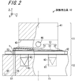
- FIG. 3 is a partially enlarged view for explaining a mechanical contact state between a DUT 1 and a contact member 13 of a contact block 12 in the test jig 10 of FIG. 2.
- FIG. 3 is a plan view of a contact block 12.
- FIG. 3 is a side view of the contact block 12.
- FIG. It is a top view which shows the detailed structure of the pallet 11 contained in the test jig
- FIG. 2 is a schematic plan view showing a configuration of a submount bonded laser chip 100 that is an example of a chip component 4 that is a device under test of the test apparatus 20 of FIG. 1. It is a typical side view which shows the structure of the submount joining laser chip 100 of FIG. 8A. It is a figure which shows the electrical symbol of the submount joining laser chip 100 of FIG. 8A.
- FIG. 8B is a schematic diagram showing a configuration of a semiconductor laser device that is the completed semiconductor device 5 including the submount bonded laser chip 100 of FIG. 8A. It is a schematic diagram which shows the structure of the test
- FIG. 3 is a diagram showing a configuration of a mounting device 120.
- FIG. 3 is a diagram showing a configuration of a mounting device 120.
- FIG. 3 is a diagram showing a configuration of a mounting device 120.
- FIG. 10 is a schematic diagram for explaining a mounting procedure of the mounting device 120.
- FIG. 10 is a schematic diagram for explaining a mounting procedure of the mounting device 120.
- FIG. 10 is a schematic diagram for explaining a mounting procedure of the mounting device 120.
- 10 is a schematic diagram for explaining a mounting procedure of the mounting device 120.
- 10 is a flowchart for explaining a placement procedure of the placement device 120.
- 10 is a flowchart for explaining a placement procedure of the placement device 120.
- FIG. 1 is a plan view schematically showing a configuration of a test apparatus 20 using a test jig 10 according to an embodiment of the present invention.
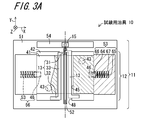
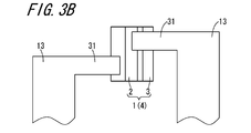
- FIG. 2 is a front view schematically showing the configuration of the test jig 10 used in the test apparatus 20 of FIG. 3A and 3B are diagrams schematically showing the configuration of the test jig 10 of FIG. 2
- FIG. 3A is a plan view of the test jig 10 of FIG. 2 as viewed from above
- FIG. 4 is an enlarged plan view of the vicinity of an external contact end portion 32 of the contact member 13.
- FIG. 4 is a partially enlarged view for explaining the mechanical contact state between the DUT 1 and the contact member 13 of the contact block 12 in the test jig 10 of FIG.
- FIG. 1 is a plan view schematically showing a configuration of a test apparatus 20 using a test jig 10 according to an embodiment of the present invention.
- FIG. 2 is a front view schematically showing the configuration of the test ji
- the test apparatus 20 conducts various tests on the device under test 1 by electrically connecting the power supply path to the device under test 1 which is the semiconductor chip 2 bonded to the submount 3 and energizing the device under test 1. Used for.
- the test jig 10 of this embodiment is provided in the above-described test apparatus 20.
- the submount 3 and the semiconductor chip 2 bonded to the submount 3 may be referred to as “chip component 4”.
- the chip component 4 is one of the components of the completed semiconductor element 5.
- the completed semiconductor element 5 includes a chip component 4 and a package 6 having terminal electrodes 7.
- the package 6 is realized by a stem or a frame, for example, and encloses the chip component 4. Since the terminal electrode 7 of the package 6 is interposed between the chip component 4 and the power supply path, the terminal electrode 7 is electrically connected to the chip component 4 in the package 6.
- the test jig 10 includes a pallet 11 and one or more contact blocks 12. Each contact block 12 has a contact member 13. In the test jig 10, one or more test objects 1 that are chip components 4 are placed on a pallet 11. The contact members 13 of the one or more contact blocks 12 are electrically connected to each test object 1 on the pallet 11. When power is supplied to each device under test 1 on the pallet 11, the contact member 13 of each contact block 12 is interposed between each device under test 1 and the power supply path outside the test jig 10.
- the test jig 10 of this embodiment When the test jig 10 of this embodiment is used, the power supply path to the device under test 1 only needs to be electrically connected to the contact member 13 of the contact block 12, and the device under test 1 that is the chip component 4. There is no need to be directly electrically connected to. That is, the contact member 13 of the contact block 12 serves as the terminal electrode 7 of the package 6 in the completed semiconductor element 5.
- the test of the present embodiment for the chip component 4 performed using the test jig 10 of the present embodiment is performed on the chip component 4 having a configuration in which the power supply path is directly electrically connected to the chip component 4. Compared to technical testing, it can be done easily.
- the test jig 10 has a size that allows easy connection between the contact member 13 of the contact block 12 and the power supply path regardless of the size of the chip component 4. 13 can be configured. Thereby, the test using the test jig 10 of the present embodiment can be easily performed as compared with the conventional test for the chip component 4 described above.
- a completed semiconductor element 5 having a configuration in which a chip component 4 is attached to a package 6 (see FIG. 8 to be described later) having terminal electrodes 7 is used as a device under test 1, and the completed semiconductor element 5.
- the contact block 12 is used instead of the terminal electrode 7 of the package 6 even if the chip component 4 as the device under test 1 is not attached to the package 6.
- the contact member 13 is interposed between the power supply path and the chip component 4.
- the test using the test jig 10 of this embodiment can be performed directly on the chip component 4 that is the semiconductor chip 2 bonded to the submount 3.
- the bonding state of the semiconductor chip 2 and the submount 3 can be directly confirmed with respect to the chip component 4.
- the semiconductor chip 2 is realized by a laser chip that oscillates laser light in response to power supply.
- the bonding state between the semiconductor chip 2 and the submount 3 affects the temperature characteristics of the semiconductor laser element itself, particularly the high temperature characteristics. Since the test using the test jig 10 of the present embodiment described above can be performed directly on the chip component 4 in which the semiconductor chip 2 is bonded to the submount 3, the semiconductor chip 2, the submount 3, and The joining state of can be directly confirmed. Therefore, the reliability of the temperature characteristics of the chip component 4 can be improved.
- the test using the test jig 10 of the present embodiment can be performed directly on the chip component 4 before the chip component 4 is mounted on the package 6 such as a stem or a frame. Accordingly, for example, after the test using the test jig 10 of the present embodiment is performed and before the chip component 4 is attached to the package 6, a number of tests are performed based on the results of the test of the present embodiment for the chip component 4. It is possible to perform screening by removing defective chip components 4 from the chip components 4.
- the manufacturing process of the semiconductor element 5 including the test using the test jig 10 of the present embodiment for the chip component 4 can eliminate in advance the defective chip component 4 from the chip component 4 attached to the package 6. .
- the manufacturing process of the semiconductor element 5 including the test using the test jig 10 of the present embodiment is more packaged than the manufacturing process of the semiconductor element 5 including the test of the prior art for the completed semiconductor element 5. Since the defect occurrence rate of the semiconductor element 5 in the completed state with the chip component 4 attached thereto can be reduced, the production efficiency of the semiconductor element 5 in the completed state can be improved.
- the manufacturing process of the semiconductor element 5 including the test using the test jig 10 of the present embodiment is finally more than the manufacturing process of the semiconductor element 5 including the test of the related art for the completed semiconductor element 5.
- the material cost and work cost required for the entire semiconductor element 5 to be shipped can be reduced.
- the manufacturing process of the semiconductor element 5 including the test of the present embodiment can suppress the manufacturing cost when the defective product is excluded from the entire finished product based on the test result.
- the chip component 4 composed of the semiconductor chip 2 bonded to the submount 3 is not only shipped with the chip component 4 mounted on the package 6, but the chip component 4 alone may be shipped as it is. . Since the test using the test jig 10 of the present embodiment can be performed directly on the chip component 4, it is possible to directly test the chip component 4 before being mounted on the package 6 before shipment. it can. Therefore, even when the chip component 4 is shipped as a single unit, the reliability of the shipped chip component 4 can be improved as compared with the related art.
- the test using the test jig 10 of the present embodiment can be performed directly and easily on the chip component 4 alone, the test on the chip component 4 is performed when the chip component 4 is shipped alone. Even if 100% inspection is not a sampling inspection, an excessively long time is not required and it can be easily performed. Thereby, the reliability of the shipped chip component 4 can be easily and sufficiently improved.
- test jig 10 of the present embodiment one or more, preferably a plurality of contact blocks 12 are configured to be detachably mounted on the pallet 11. As a result, each contact block 12 can be individually maintained and managed, and maintenance for a plurality of contact blocks 12 is facilitated. Thereby, the usability of the test jig 10 of this embodiment is improved.
- each contact block 12 is detachable from the pallet 11 so that the electrical characteristics of the multiple contact blocks 12 can be easily determined individually. Therefore, only the non-defective contact block 12 can be actually used in the test jig 10 of the present embodiment.
- each contact block 12 is detachable from the pallet 11, so that compared to the test jig 10 in which the contact block 12 is permanently installed on the pallet 11,
- the test jig 10 of the present embodiment can replace only the defective contact block 12 quickly and easily when any one of the contact blocks 12 has a problem. This facilitates the maintenance of a large number of contact blocks 12.
- each contact block 12 can be easily attached to and detached from the pallet 11, so that when the DUT 1 is placed on the pallet 11, the contact block 12 is removed from the pallet 11. It is possible to remove it. Therefore, when the DUT 1 is placed on the pallet 11, interference objects such as the contact block 12 and the positioning mechanism of the DUT 1 are placed around the planned position 17 where the DUT 1 in the pallet 11 should be placed. It is possible to place the device under test 1 on the pallet 11 in a state that does not exist. As a result, it is possible to simplify the mechanism relating to the placement of the DUT 1 on the pallet 11 and the mechanism relating to the mounting of the contact block 12 on the pallet 11.
- each contact block 12 is detachable from the pallet 11, the structure of the DUT 1 is common to the contact block 12 having a structure that matches the structure of the DUT 1. It is possible to replace only the contact block 12 when the structure of the device under test 1 is changed. As a result, it can be easily applied to various types of test objects 1.
- the contact member 13 of the contact block 12 is a member made of a conductive material, and a part of the contact member 13 is mounted when the contact block 12 is mounted on the pallet 11.
- the contact member 13 of the contact block 12 is mechanically contacted between the device under test 1 and the contact member 13 made of a conductive material. Can be electrically connected to the device under test 1.
- the contact block 12 having a structure that can be freely attached to and detached from the pallet 11 is used, and the contact member 13 made of a conductive material when the pallet 11 is mounted is the test object 1.
- the labor of handling the test jig 10 of the present embodiment can be reduced, and the difficulty of testing using the test jig 10 of the present embodiment can be reduced.
- the contact member 13 of the contact block 12 is realized by a leaf spring.
- the contact member 13 made of a leaf spring is in contact with each device under test 1 while the contact member 13 of each contact block 12 is in mechanical contact when the contact block 12 is mounted on the pallet 11 on which the device under test 1 is placed. Then, each of the devices under test 1 is pressed. Thereby, the contact member 13 of each contact block 12 can maintain the position and orientation of each device under test 1 while achieving electrical connection to each device under test 1 on the pallet 11.
- the configuration of the pallet 11 can be simplified. Further, it is not necessary for the contact block 12 to have a separate holding mechanism for the position and orientation of each device under test 1, and the holding member can also serve as a contact member 13 for electrical connection to each device under test 1. Therefore, it is possible to prevent the configuration of the contact block 12 from becoming complicated. As a result, it is possible to easily electrically connect the external power supply path and the DUT 1 while maintaining the position and orientation of the DUT 1 using the contact block 12 and the pallet 11 having a simple configuration. Can do. Therefore, it is possible to realize a test jig 10 that is easy to use.
- the contact member 13 having a leaf spring structure holds the position and orientation of the DUT 1 while being electrically connected to the DUT 1 with a very simple configuration. Is possible. Since the configuration of the contact member 13 of this embodiment is simple, the maintenance management of the contact block 12 can also be simplified. Thereby, the configuration of the test jig 10 is further simplified, and the usability of the test jig 10 is further improved.
- each contact block 12 attached to the pallet 11 is a predetermined electrical that can be interposed between the DUT 1 and the power supply path outside the test jig 10. It is determined in advance that it has characteristics. That is, a non-defective contact block 12 having electrical characteristics capable of interposing between the device under test 1 and the power supply path among a large number of contact blocks 12 is selected in advance, and the selected non-defective contact block 12 is a pallet. 11 and a test using the test jig 10 of this embodiment is performed. Thereby, in the test using the test jig 10 of the present embodiment, the erroneous determination of the test due to the failure of the contact block 12 can be prevented. This also improves the usability of the test jig 10 of this embodiment.
- the contact block 12 is detachable from the pallet 11, so that the electrical characteristics of the contact block 12 are inspected with the contact block 12 removed from the pallet 11. Is possible. Compared to the case where each contact block 12 is inspected while a large number of contact blocks 12 are mounted on the pallet 11, the case where the contact block 12 removed from the pallet 11 is inspected as in this embodiment. There is little trouble of 12 inspections. Thus, since the labor of the inspection of the contact block 12 is reduced, the usability of the test jig 10 of this embodiment is further improved.
- the test jig 10 of the present embodiment is detachably attached to the test apparatus 20.
- the test apparatus 20 using the test jig 10 holds one or more devices 1 to be tested, which are the semiconductor chips 2 bonded to the submount 3, by the test jig 10 described above, and holds each device 1 to be tested. Electric power is supplied to each device under test 1 held by the test jig 10 via each contact block 12 while controlling the temperature environment of the test jig 10.
- the test apparatus 20 can test the chip component 4 by driving the device under test 1 that is the chip component 4 while controlling the temperature environment.
- the above-described test jig 10 is detachably attached, and the attached test jig 10 is used for the test.
- the test power supply unit 22 does not need to be directly and electrically connected to the device under test 1 that is the chip component 4, and the test power is supplied to the contact member 13 of the contact block 12 of the test jig 10.
- the part 22 should just be electrically connected.
- the test apparatus 20 using the test jig 10 described above has a chip component as compared with the test apparatus 20 of the prior art in which the test power supply unit 22 is directly electrically connected to the chip component 4. 4 can be easily tested. This also makes it possible to easily perform the test on the chip component 4 in the test apparatus 20 of the present embodiment as compared with the conventional test on the completed semiconductor element 5.
- the test apparatus 20 of the present embodiment can directly perform a test on the chip component 4 that is the semiconductor chip 2 bonded to the submount 3 while controlling the temperature environment. Therefore, the manufacturing process of the semiconductor element 5 including the test by the test apparatus 20 of the present embodiment can improve the production efficiency of the semiconductor element 5 in a completed state, and can suppress the manufacturing cost due to defective products. Therefore, when the chip component 4 is shipped as a single unit, 100% inspection of the chip component 4 can be easily performed, so that the reliability of the shipped chip component 4 can be easily and sufficiently improved.
- the pallet 11 of the test jig 10 preferably has the suction holes 14.
- the DUT 1 is placed at a position that overlaps the opening at one end of the suction hole 14 on the pallet 11, and the gas in the suction hole 14 is in a state where each DUT 1 is placed on the pallet 11.
- Suction is performed by the vacuum suction source 23.
- the position and orientation of the device under test 1 in the test jig 10 is maintained by vacuum suction.
- the test apparatus 20 of the present embodiment can be easily combined with the suction hole 14 of the pallet 11 of the test jig 10 and the vacuum suction source 23 as a holding mechanism for the position and orientation of the DUT 1 on the pallet 11. New configuration is added. Therefore, the test apparatus 20 of this embodiment not only holds the position and orientation of the DUT 1 using the contact member 13 of the contact block 12, but also holds the position and posture of the DUT 1 by vacuum suction. Can do. Therefore, since the position and orientation of the DUT 1 in the test jig 10 is more reliably maintained, the usability of the test apparatus 20 of the present embodiment is improved.
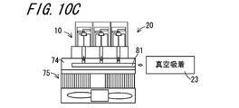
- the temperature environment control unit 21 includes a constant temperature plate 74 that contacts the pallet 11 and transmits heat, and a heating and cooling unit 75 that heats and cools the constant temperature plate 74.
- a communication hole 81 that can communicate with the suction hole 14 of the pallet 11 is formed in the constant temperature plate 74, and the gas in the communication hole 81 is also sucked when the gas in the suction hole 14 of the pallet 11 is sucked.
- the contact property between the pallet 11 and the constant temperature plate 74 is improved, so that the heat of the constant temperature plate 74 is efficiently transmitted to the pallet 11. Therefore, since the temperature control of the test jig 10 is more reliably executed, the usability of the test apparatus 20 of the present embodiment is improved.
- the semiconductor chip 2 of the device under test 1 is formed of a laser diode. That is, the chip component 4 that is the device under test 1 of the test apparatus 20 of the present embodiment is realized by a submount bonded laser chip having a configuration in which a laser diode is connected to the submount 3, and is completed including the chip component 4.
- the semiconductor element 5 in the state is realized by a semiconductor laser element.
- the submount bonded laser chip emits predetermined light in response to power supply from an external power supply path.
- the device under test 1 is a submount bonded laser chip
- the light emitted from the submount bonded laser chip as the device under test 1 is reflected by the reflecting mirror 15 in the test apparatus 20 of the present embodiment. It is guided to the light receiving element 25.
- the position of the light receiving element 25 can be arbitrarily set regardless of the emission direction of the submount bonded laser chip, and the degree of freedom of the configuration of the test apparatus 20 of the present embodiment is improved.
- the laser beam is emitted from the submount bonded laser chip on the side where the external electrode 28 for contacting the contact block 12 included in the test power supply unit 22 is located with respect to the device under test 1. Light is guided.
- the external electrode 28 and the light receiving element 25 of the test power supply unit 22 are preferably supported by a single support substrate 26, and the external electrode 28 and the light receiving element 25 are supported.
- the entire substrate 26 is moved away from the test jig 10.
- the external terminal of the test electrode supply unit and the light receiving element 25 for inspection are integrated and separated from each other.
- the test apparatus 20 of this embodiment can share the drive system of the constituent elements to simplify the apparatus configuration.
- the support substrate 26 is moved by the substrate moving unit 27 to a standby position away from the constant temperature plate 74 of the temperature environment control unit 21 rather than the position at the time of performing the test. It is done. As a result, with the movement of the support substrate 26, the light receiving element 25 supported by the support substrate 26 and the external electrode 28 of the test power supply unit 22 are also separated from the constant temperature plate 74.
- the support substrate 26 at the standby position is moved from the standby position to the position at the time of the test by the substrate moving unit 27 when the test is performed.
- the light receiving element 25 supported by the support substrate 26 and the external electrode 28 of the test power supply unit 22 also approach the constant temperature plate 74 rather than the standby position.
- the test apparatus 20 of the present embodiment when the test jig 10 is attached to and detached from the test apparatus 20, the distance between the support substrate 26 and the constant temperature plate 74 is wider than when the test is performed. Can be easily attached to and detached from the test apparatus 20. Therefore, the usability of the test apparatus 20 of this embodiment is improved.
- FIG. 5 is a diagram showing a detailed configuration of the pair of contact members 13 provided in the contact block 12 in the test jig 10 of the present embodiment.
- the pair of contact members 13 have the same basic configuration and different actual dimensions. Therefore, only one of the pair of contact members 13 will be described with reference to FIG.
- the approaching / separating direction between the contact block 12 and the pallet 11 is defined as the “Z direction”
- the longitudinal direction of the contact member 13 of the contact block 12 described later is defined as the “Y direction”.
- the direction orthogonal to the direction is defined as “X direction”.
- the contact member 13 is made of a conductive material. If an electrode or a terminal formed of a conductive material mechanically contacts the contact member 13, the electrode or terminal and the contact member 13 are electrically connected.
- the detailed configuration of the contact member 13 is not particularly limited as long as the above function can be realized.
- the contact member 13 is made of beryllium copper, and the surface thereof is plated with gold.
- the contact member 13 has a shape in which both ends of the elongated plate-like member protrude in opposite directions in the width direction of the plate-like member, and has a substantially B shape as a whole.
- the protrusion at one end in the longitudinal direction of the contact member 13 is in mechanical contact with the device under test 1 to make an electrical connection.
- the protruding portion at the other end in the longitudinal direction of the contact member 13 is in mechanical contact with the power supply terminal from the outside of the test jig 10 to make an electrical connection.
- the external electrode 28 of the test power supply unit 22 is formed on the protruding portion at the other end in the longitudinal direction of the pair of contact members 13. Mechanical contact.
- one end of the contact member 13 in the longitudinal direction that should be in mechanical contact with the DUT 1 is referred to as an “internal contact end 31”, and various electrodes outside the test jig 10.
- the other end portion to be mechanically contacted with each other is referred to as “external contact end portion 32”.
- the central portion in the longitudinal direction excluding the inner contact end portion 31 and the outer contact end portion 32 of the contact member 13 is referred to as a “center bending portion 33”.
- the protrusions of the internal contact end portions 31 of the pair of contact members 13 can mechanically contact the anode and cathode of the device under test 1 when the contact block 12 is mounted on the pallet 11, respectively.
- the shape and position are determined so that That is, the shape and size of the protruding portion of the internal contact end portion 31 of the pair of contact members 13 are determined according to the configuration of the device under test 1.
- the protruding portions of the external contact end portions 32 of the pair of contact members 13 can be easily mechanically contacted with various external electrodes of the test jig 10 regardless of the size of the device under test 1. Thus, it is formed sufficiently large.
- mechanical contact with various external electrodes of the test jig 10 is facilitated regardless of the size of the device under test 1. Ten usability is improved.
- the external contact end 32 of the contact member 13 is fixed in the contact block 12.
- the inner contact end 31 of the contact member 13 is displaceable in the Z direction that is close to and away from the DUT 1 when the contact block 12 is placed on the pallet 11 with the outer contact end 32 being a fixed end as a fulcrum. is there.
- the central bending portion of the contact member 13 is configured to be able to bend in the Z direction according to the displacement of the internal contact end portion 31 with the external contact end portion 32 as a fulcrum.
- the contact block 12 When the contact block 12 is placed on the pallet 11, the protruding portion of the internal contact end 31 of the contact member 13 comes into contact with the DUT 1 on the pallet 11. With the mechanical contact of the projecting portion of the inner contact end 31 of the contact member 13 with the device under test 1, the central bending portion 33 of the contact member 13 bends in the Z direction. As a result, the contact member 13 presses the device under test 1. As an example, the contact member 13 presses the device under test 1 with a force of about 0.05 N.
- the contact member 13 forms a leaf spring structure, the configuration of the contact member 13 that electrically connects the device under test 1 and holds the device under test 1 can be simplified. The manufacturing cost and management maintenance cost of the tool 10 can be reduced.
- FIG. 6A to 6C are views showing a detailed configuration of the contact block 12 provided in the test jig 10 of this embodiment
- FIG. 6A is a front view of the contact block 12
- FIG. FIG. 6C is a side view of the contact block 12.
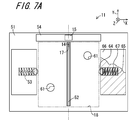
- 7A and 7B are diagrams showing a detailed configuration of the pallet 11 included in the test jig 10
- FIG. 7A is a plan view of the pallet 11
- FIG. 7B is an inside of the pallet 11 of the present embodiment.
- 2 is a partially enlarged view showing the vicinity of the planned position 17 of the DUT 1 in the mounting table 52 described later.
- the detailed configuration of the contact block 12 shown in FIGS. 6A to 6C and the detailed configuration of the pallet 11 shown in FIGS. 7A and 7B are examples of the detailed configuration of the contact block 12 and the pallet 11, and are not limited thereto. Absent.
- the approaching / separating direction between the contact block 12 and the pallet 11 is defined as the “Z direction”
- the longitudinal direction of the contact member 13 of the contact block 12 described later is defined as the “Y direction”.
- the direction orthogonal to the direction is defined as “X direction”.
- the contact block 12 has an electrical connection between the device under test 1 and an external member of the test jig 10 and has a function of fixing the chip component 4 as the device under test 1 to the pallet 11.
- the contact block 12 further includes a cover body 41, a base plate 42, and block positioning pins 43.
- the pallet 11 further includes a base 51, a mounting table 52, a fixing mechanism 53, and a table 54.
- the base plate 42 is formed from a PEEK material or the like
- the cover body 41 is formed from aluminum or the like
- the block positioning pins 43 are formed from stainless steel or the like.
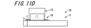
- a reference position 18 to which one or more contact blocks 12 are to be mounted is set in advance on the upper surface of the base 51.
- a mounting table 52, a pair of fixing mechanisms 53, a reflecting mirror 15, and a table 54 are provided for a single reference position 18 on the upper surface of the base 51.
- FIGS. 7A and 7B in the pallet 11 on which one or more devices to be tested 1 are to be placed, only the configuration within the range related to the single device to be tested 1 is shown in detail.
- the actual pallet 11 has a configuration in which the configurations shown in FIGS. 7A and 7B are arranged by the number of the test objects 1 to be placed.
- a rectangular parallelepiped cover body 41 is placed on the upper surface of the rectangular plate-shaped base plate 42.
- the base plate 42 is fixed to the bottom surface of the cover body 41 by, for example, screwing.
- the depth of the cover body 41 in the Y direction is shorter than the depth of the base plate 42 in the Y direction.
- the base plate 42 and the cover body 41 hold various components of the contact block 12.
- the base plate 42 insulates the contact member 13 and the pallet 11.
- a bottom groove 45 is formed at the center of the bottom of the cover body 41.
- the bottom groove 45 of the cover body 41 opens to the bottom surface side of the cover body 41 and penetrates the cover body 41 in the Y direction.
- a slit 48 is formed at a position facing the bottom groove 45 of the cover body 41 when fixed.
- the slit 48 of the base plate 42 extends in the same direction as the longitudinal direction of the bottom groove 45 of the cover body 41 and is narrower than the bottom groove 45.
- the external contact end portion 32 and the internal contact end portion 31, which are both longitudinal ends of the contact member 13, are located outside the cover body 41.
- the central bending portion 33 which is the central portion in the longitudinal direction of the contact member 13, can be freely bent in the normal direction Z of the base plate 42 with the external contact end portion 32 of the contact member 13 as a fulcrum. It is disposed in a space surrounded by the bottom groove 45 and the base plate 42.
- the height of the bottom groove 45 of the cover body 41 in the Z direction is sufficiently high so as not to hinder the bending of the contact member 13 accompanying the contact of the internal contact end 31 of the contact member 13 with the device under test 1.
- the mounting table 52 is a member for mounting the DUT 1.
- the rectangular parallelepiped mounting table 52 is fixed to the center in the X direction in the reference position 18 on the upper surface of the base 51 so that the longitudinal direction is parallel to the Y direction.
- the planned position 17 on which the DUT 1 is to be placed is set on the top surface of the placement table 52.
- one end of the suction hole 14 of the pallet 11 opens at the center of the planned position 17 of the pallet 11 when viewed from the Z direction that is the normal direction of the base 51. Specifically, the suction hole 14 of the pallet 11 passes through the mounting table 52 and the base 51, and the other end of the suction hole 14 is opened on the bottom surface of the base 51.
- the pair of substantially plate-like contact members 13 are attached to the base plate 42 so that the external contact end portion 32 which is the other end in the longitudinal direction of the contact member 13 is fixed.
- the distance between the central bending portions 33 of the pair of contact members 13 attached to the base plate 42 is wider than the width of the mounting table 52 of the pallet 11 in the X direction.
- the mounting position of the DUT 1 becomes one step higher than the upper surface of the base 51.
- the configuration in which the DUT 1 is mounted on the mounting table 52 on the upper surface of the base 51 as in this embodiment is more contact block than the configuration in which the DUT 1 is directly mounted on the upper surface of the base 51.
- one or more block positioning pins 43 are fixed to the bottom surface of the base plate.
- a block fitting recess 61 to which each block positioning pin 43 should be fitted is formed on the upper surface of the base 51.
- the two block positioning pins 43 are disposed, for example, at diagonal corners of the base plate 42.
- the block positioning pin 43 may be provided on the pallet 11 side, and the block fitting recess 61 may be formed on the contact block 12 side.
- the block positioning pin 43 and the block fitting recess 61 are configured to fix the position of the contact block 12 when the contact block 12 is mounted on the pallet 11.
- the block positioning pins 43 of the contact block 12 are fitted into the block fitting recesses 61 of the pallet 11.
- the movement of the contact block 12 in the direction parallel to the upper surface of the base 51 is hindered, so that the contact block 12 is fixed to the reference position 18 of the pallet 11.
- the block positioning pin 43 and the block fitting recess 61 preferably also serve as a positioning guide for the contact block 12 and the pallet 11.
- the contact block 12 is approximately positioned at a predetermined position of the pallet 11 so that the inverted conical block positioning pin 43 and the cylindrical hole-shaped block fitting recess 61 can be fitted, the block positioning pin 43
- the position of the contact block 12 with respect to the pallet 11 is naturally adjusted in accordance with the behavior of fitting into the block fitting recess 61. Therefore, if the block positioning pin 43 and the block fitting recess 61 are provided, the relative position between the pallet 11 and the contact block 12 is naturally adjusted without detailed positioning, which is convenient.
- a pair of fixing mechanisms 53 are disposed on both sides in the X direction of the reference position 18 on which the contact block 12 on the pallet 11 is to be placed.
- fixing concave portions 46 are provided on both side surfaces of the cover body 41 in the X direction.
- a single contact block 12 is provided with a pair of fixing mechanisms 53 and a pair of fixing recesses 46 having the same shape.
- the fixing mechanism 53 on the pallet 11 side and the fixing recess 46 on the contact block 12 side are combined to form a mounting mechanism 56 for detachably mounting the contact block 12 on the pallet 11.
- the single fixing mechanism 53 includes a stopper ball 64, a ball spring 65, and a fixing member 66.
- a housing recess 67 that opens to the one side face is formed. Stopper balls 64 are stored in the storage recesses 67 so as to protrude freely from the storage recesses 67.
- a ball spring 65 is interposed between the stopper ball 64 and the bottom of the storage recess 67 so as to be extendable in the X-axis direction.
- the spring force of the ball spring 65 acts in a direction to push the stopper ball 64 from the storage recess 67 inside the fixing member 66 to the outside of the storage recess 67.
- the fixing recesses 46 on both side surfaces in the X direction of the cover body 41 have a shape in which a part of the stopper ball 64 of the fixing mechanism 53 can be fitted.
- the stopper ball 64 stands by in a state where a part of the stopper ball 64 protrudes from the storage recess 67 by the ball spring 65.
- the stopper ball 64 is stored inside the storage recess 67 against the spring force. A part of the stopper ball 64 stored in the storage recess 67 protrudes again from the storage recess 67 by the spring force.
- the standby distance of the stopper ball 64 of the pair of fixing mechanisms 53 is slightly narrower than the width of both side surfaces in the X direction of the cover body 41 of the contact block 12.
- the distance between the two side surfaces of the two fixing mechanisms 53 facing each other in the X direction is approximately the same as or slightly wider than the width of the contact block 12 in the X direction. Therefore, as the contact block 12 approaches and separates from the base 51 of the pallet 11, the external force due to the contact of the cover body 41 of the contact block 12 is applied to the stopper ball 64 of the fixing mechanism 53 of the pallet 11, and the position of the stopper ball 64 is changed.
- the stopper ball 64 of the fixing mechanism 53 of the pallet 11 is fitted to and detached from the fixing recess 46 of the cover body 41 of the contact block 12 by moving in the X direction. As a result, the contact block 12 is detachably attached to the pallet 11.
- the contact block 12 moves in a direction close to the base 51 of the pallet 11.
- the contact block 12 is inserted between a pair of fixing mechanisms 53 arranged on both sides of the reference position 18, and both side surfaces in the X direction of the cover body 41 of the contact block 12 are a pair of fixing mechanisms 53.
- the stopper ball 64 comes into contact. Since the stopper ball 64 is spherical, with the movement of the contact block 12, both side surfaces in the X direction of the cover body 41 apply an external force against the spring force to the stopper ball 64 so that the stopper ball 64 is stored in the storage recess 67. .
- the block positioning pin 43 of the contact block 12 is inserted into the block fitting recess 61 of the base 51 of the pallet 11. Mating.
- the stopper ball 64 of the fixing mechanism 53 of the pallet 11 is fitted into the fixing recess 46 of the cover body 41 of the contact block 12. As a result, the contact block 12 is detachably attached to the pallet 11.
- the reflecting mirror 15 reflects light emitted from the device under test 1 in a predetermined direction.
- the table 54 supports the reflecting mirror 15 at an angle that matches the direction in which the light emitted from the DUT 1 should be reflected. If the optical path of light is refracted by 90 degrees by the reflecting mirror 15, the mirror base 54 supports the reflecting mirror 15 at an angle inclined by 45 degrees with respect to the light emitting direction.
- the reflecting mirror 15 of the pallet 11 is preferably in the direction of light emission from the submount bonded laser chip. The light is emitted from the submount bonded laser chip and reflected in a direction that forms 90 degrees with respect to the light emission direction.
- the light receiving element 25 In the configuration in which the light receiving element 25 is installed in parallel to the light emitting surface of the submount bonding laser chip, a space for providing the light receiving element 25 is required before the light emitting surface of the submount bonding laser chip, and thus the size of the pallet 11 is increased. easy.
- the reflecting mirror 15 inclined by 45 degrees with respect to the light-emitting surface of the submount bonding laser chip By using the reflecting mirror 15 inclined by 45 degrees with respect to the light-emitting surface of the submount bonding laser chip, the light emitting direction from the submount bonding laser chip is bent by 90 degrees to thereby submount the submount. Since the light receiving element 25 can be installed perpendicular to the light emitting surface of the bonded laser chip, the pallet 11 and the test apparatus 20 can be downsized.
- the test apparatus 20 of the present embodiment further includes a control unit 71 and an output unit 72.
- the test power supply unit 22 includes a drive circuit 29 in addition to the external electrode 28.
- the heating / cooling unit 75 of the temperature environment control unit 21 includes a Peltier element 85, a heat radiation fan 87, a heat radiation fin 86, and a temperature controller 84.
- a jig positioning pin 82 for positioning the test jig 10 is provided on the upper surface of the constant temperature plate 74 of the temperature environment control unit 21.
- the control unit 71 controls components of the test apparatus 20 in order to perform a test on the device under test 1. For example, the control unit 71 obtains the driving result of the device under test 1 supplied with power under the temperature environment controlled by the temperature environment control unit 21, and determines whether the device under test 1 is good or bad based on the obtained driving result. to decide.
- the test result of the DUT 1 is output to the output unit 72.
- the output unit 72 presents the test result of the device under test 1 to the user of the test apparatus 20.
- the output unit 72 transmits the test result to another device in the manufacturing process including the test device 20.
- the drive circuit 29 of the test power supply unit 22 responds to a control command from the control unit 71 of the test apparatus 20, and connects the device under test 1 to the device under test 1 in the test jig 10 via the external electrode 28.
- the power for driving 1 is supplied.
- the drive circuit 29 of the test power supply unit 22 is interposed between the light receiving element 25 and the control unit 71 and transmits a signal from the light receiving element 25 to the control unit 71. That is, the drive circuit 29 of the test power supply unit 22 operates as a so-called driver circuit.
- the upper surface of the Peltier element 85 is in mechanical contact with the bottom surface of the constant temperature plate 74.
- the radiation fins 86 are in mechanical contact with the bottom surface of the Peltier element 85.
- the heat radiating fan 87 generates an air flow that passes through the heat radiating fins 86.
- the temperature controller 84 drives the Peltier element 85 so that the temperature environment of the test jig 10 becomes a temperature environment instructed by the control unit 71. Let In response to the control from the temperature controller 84, one of the top and bottom surfaces of the Peltier element 85 generates heat and the other surface absorbs heat.
- the jig positioning pin 82 and the jig fitting recess 62 are configured to fix the position of the test jig 10 when the test jig 10 is attached to the test apparatus 20.
- the constant temperature plate 74 is placed in the jig fitting recess 62 on the bottom surface of the base 51 of the pallet 11 of the test jig 10.
- the jig positioning pins 82 on the upper surface of the upper side of the upper side are fitted.
- the jig positioning pins 82 and the jig fitting recesses 62 are preferably positioning guides between the test jig 10 and the constant temperature plate 74, similarly to the combination of the block positioning pins 43 and the block fitting recesses 61. Doubles as As a result, usability of the test apparatus 20 is improved.
- the jig positioning pin 82 may be provided on the test jig 10 side, and the jig fitting recess 62 may be formed on the constant temperature plate 74 side.
- the test apparatus 20 uses the chip component 4 alone instead of the completed semiconductor element 5 in which the chip component 4 is sealed in the package 6 including the terminal electrode 7. And Further, in the test apparatus 20 of this embodiment, the chip component 4 that is the device under test 1 is used for testing via the contact member 13 of the contact block 12 of the test jig 10 instead of the terminal electrode 7 of the package 6. It is electrically connected to the power supply unit 22.
- the test apparatus 20 of the present embodiment when the chip component 4 is configured to emit light such as a laser diode, the light emission state of the chip component 4 is observed as a test result.
- the test result of the chip component 4 is not limited to the light emission state, and it is only necessary to obtain an output capable of estimating the driving state of the chip component 4 such as an output state of an electric signal.
- the test apparatus 20 of the present embodiment also detects the electrical output from the chip component 4 in the contact block 12 of the test jig 10. What is necessary is just to take out through the contact member 13 of this.
- the chip component 4 that is the device under test 1 of the test apparatus 20 of the present invention includes the semiconductor chip 2 bonded to the submount 3.
- the semiconductor chip 2 is a component that exhibits a predetermined function in response to power supply.
- the submount 3 is, for example, a component that places and supports the semiconductor chip 2 and is directly bonded to the semiconductor chip 2.
- the semiconductor chip 2 is configured by stacking a plurality of functional layers including a semiconductor layer.
- the semiconductor chip 2 is realized by a so-called die formed by cutting a wafer in which a large number of circuits are formed on the surface layer into a predetermined shape.
- the submount 3 includes, for example, an electrode layer that is in mechanical contact with the functional layer of the semiconductor chip 2 and a heat dissipation layer for heat generated from the semiconductor chip 2.
- the completed semiconductor element 5 has a configuration in which the chip component 4 is enclosed in a package 6 including the terminal electrode 7 and the chip component 4 and the terminal electrode 7 are electrically connected.
- the package 6 is realized by, for example, a so-called stem 101 or a frame described later.
- the chip component 4 encapsulated in the package 6 and the terminal electrode 7 of the package 6 are electrically connected, for example, by bonding a connecting wire 8.
- the package 6 including the expensive stem 101 and the wire 8 is necessary, and the chip component 4 is enclosed in the package 6.
- Various assembly processes are required for electrical connection.
- the test apparatus 20 Since the test apparatus 20 according to the present embodiment performs various tests on the chip component 4 before being attached to the package 6 instead of the completed semiconductor element 5, it is possible to determine whether the chip component 4 alone is good or bad. .
- the quality of the chip component 4 alone is judged before being attached to the package 6, and all the chip components 4 not mounted on the package 6 are defective. Only the non-defective chip component 4 is attached to the package 6 without the chip component 4. Therefore, in the manufacturing process of this embodiment, it is possible to prevent the defective chip component 4 from being attached to the good package 6 and the completed semiconductor element 5 itself from being defective.
- the manufacturing process including the test apparatus 20 of the present embodiment for the chip component 4 is more expensive than the related art manufacturing process including the test apparatus 20 for the semiconductor element 5 in the completed state. Can be reduced.
- chip component 4 of the present embodiment there is a chip component 4 in which the semiconductor chip 2 is realized by a laser diode 90.
- the “chip component 4 in which the semiconductor chip 2 is the laser diode 90” may be referred to as the “submount junction laser chip 100”.
- FIG. 8A is a schematic plan view showing a configuration of a submount bonded laser chip 100 that is an example of a chip component 4 that is a device under test of the test apparatus 20 of the present embodiment.
- FIG. 8B is a schematic side view showing the configuration of the submount bonded laser chip 100 of FIG. 8A.
- FIG. 8C is a diagram showing electrical symbols of the submount bonded laser chip 100 of FIG. 8A.
- FIG. 8D is a schematic diagram showing a configuration of a semiconductor laser element that is the completed semiconductor element 5 including the submount bonded laser chip 100 of FIG. 8A.
- a laser diode 90 which is one type of semiconductor chip 2, has a PN connection layer in which a P-type semiconductor layer 91 and an N-type semiconductor layer 92 are joined, and functions as a diode as shown in the circuit diagram of FIG. 8C. To do.
- An anode 93 (anode) is provided on one semiconductor layer side of the PN connection layer, and a cathode 94 (cathode) is provided on the other semiconductor layer side of the PN connection layer.
- the laser diode 90 is formed including a semiconductor layer of gallium arsenide (Gallium_Arsenide: GaAs).
- the submount 3 joined to the laser diode 90 has a function of radiating heat generated by the laser diode 90.
- the submount 3 includes, for example, an upper electrode layer 97 made of a conductive material and a lower insulator layer 98 made of an insulator.
- An upper surface electrode layer 97 is disposed so as to overlap the surface of the lower insulator layer 98 on the laser diode 90 side.
- the submount 3 includes a heat dissipation layer made of aluminum nitride.
- the laser diode 90 is positioned on the upper surface of the submount 3 so that either the anode 93 or the cathode 94 of the laser diode 90 is mechanically and electrically connected to the upper electrode layer 97. Bonded to the electrode layer 97. Therefore, the external electrode 28 of the power supply path for supplying power to the submount junction laser chip 100 is electrically connected to either one of the laser diodes 90 via the upper surface electrode layer 97 of the submount 3. To do.
- the light emitting point 95 at the junction boundary between the P-type semiconductor layer 91 and the N-type semiconductor layer 92 emits light.
- the light emitted from the light emitting point 95 of the submount bonded laser chip 100 is emitted outside the submount bonded laser chip 100.
- the completed semiconductor laser element including the submount bonded laser chip 100 includes, as an example, a submount bonded laser chip 100 that is a laser chip bonded to the submount 3, a stem 101 and a frame. And bonding to the package 6 realized by the above, and the anode 93 and the cathode 94 of the submount bonding laser chip 100 are wire-bonded to the pair of terminal electrodes 7 of the package 6.
- the completed semiconductor laser device has a so-called CAN package 6.
- the completed semiconductor laser device having the CAN package 6 includes a stem 101 including a terminal electrode 7 and a cap 102.
- the stem 101 has a substantially cylindrical base 104 and a mounting portion 105 on which the submount bonded laser chip 100 is mounted.
- the mounting portion 105 of the stem 101 protrudes from one surface in the axial direction of the base portion 104 of the stem 101.
- the stem 101 has a function of radiating heat generated from the submount bonded laser chip 100.
- the stem 101 is formed of a metal having high thermal conductivity and high conductivity.
- a pair of terminal electrodes 7 protrude from the other axial surface of the base 104 of the stem 101.
- the pair of terminal electrodes 7 includes a plus (+) side terminal electrode 106 and a ground side terminal electrode 107 for supplying a current for driving the semiconductor laser element in a completed state.
- the plus-side terminal electrode 106 is provided on the stem 101 via an electrically insulating member, and is electrically insulated from the stem 101.
- the plus side terminal electrode 106 and the ground side terminal electrode 107 are electrically connected to the submount bonding laser chip 100 mounted on the stem 101.
- the cap 102 is formed in a bottomed cylindrical shape having a size such that the peripheral edge of one surface of the base 104 is exposed, and is provided coaxially with the base 104.
- the bottomed cylindrical cap 102 covers the submount bonding laser chip 100 and the mounting portion 105 of the stem 101, and the opening is bonded to the base portion 104 at one surface of the base portion 104 of the stem 101.
- the cap 102 also has a function of radiating heat generated from the submount bonding laser chip 100.
- the cap 102 has a transmission part at the bottom part that transmits laser light emitted from the submount bonding laser chip 100. About the part except the permeation
- the detailed configuration of the semiconductor laser element is not particularly limited as long as the above functions can be realized.
- the semiconductor laser element may be configured to emit light for reading / writing on a CD (Compact Disk) or reading / writing on a DVD (Digital Versatile Disk), or configured to output light of a single wavelength or two wavelengths. It may be.
- the emission wavelength of the submount bonded laser chip 100 is preferably 400 nm to 1300 nm.
- the semiconductor used for the submount junction laser chip 100 is preferably a gallium arsenide-based semiconductor.
- the constituent material of the stem 101 is not particularly limited, and examples thereof include aluminum.
- the constituent material of the terminal electrode 7 is not specifically limited, For example, copper etc. are mentioned.
- the constituent material of the part excluding the transmission part of the cap 102 is not particularly limited, and examples thereof include aluminum.
- the DUT 1 is the submount bonded laser chip 100
- both in the current control mode (Auto-Current Control: ACC) drive and in the power drive mode (Auto-Power Control: APC) drive may be fed back and measured for quality determination of the submount bonded laser chip 100.
- FIG. 9A is a schematic diagram showing the configuration of an inspection apparatus 110 for inspecting the electrical characteristics of the contact block 12 of the test jig 10 of this embodiment.
- FIG. 9B is a schematic diagram showing the configuration of the electrical system of the inspection apparatus 110 of the present embodiment.
- 9A and 9B is a non-defective contact block capable of interposing between the device under test 1 and the power supply path from among a large number of contact blocks 12 in the test jig 10 of the present embodiment.
- 12 is a device for preliminarily sorting 12.
- a test using the test jig 10 of the present embodiment is performed using only the non-defective contact blocks 12 selected by the inspection apparatus 110 of the present embodiment.
- the inspection apparatus 110 of the present embodiment is an apparatus for inspecting the electrical characteristics of the contact block 12 used in the test jig 10 of the present embodiment described above.
- the inspection apparatus 110 includes a pseudo pallet 111, a pseudo chip 112, an inspection power supply unit 113, and a resistance measurement unit 114.
- the pseudo chip 112 is an electrode having the same shape as the single device under test 1 of the test jig 10 of the present embodiment.
- the pseudo pallet 111 is a member having the same shape as the pallet 11 of the test jig 10 of the present embodiment.
- the pseudo chip 112 is placed on the pseudo pallet 111.
- a contact block 12 as an object to be inspected is mounted on the pseudo pallet 111 on which the pseudo chip 112 is placed.
- the positional relationship among the pseudo chip 112, the pseudo pallet 111, and the contact block 12 in the inspection device 110 is the same as the positional relationship between the device under test 1, the pallet 11 and the contact block 12 in the test device 20.
- the contact block 12 is supplied with electric power via the contact member 13 of the contact block 12 to the pseudo chip 112 on the pseudo pallet 111.
- the contact resistance is measured. Based on the measured contact resistance of the contact block 12, it is determined whether or not the contact block 12 is non-defective.
- the inspection apparatus 110 of the present embodiment can easily measure the electrical characteristics of the contact block 12 by mounting the contact block 12 on the pseudo pallet 111 on which the pseudo chip 112 is mounted. Therefore, the inspection apparatus 110 of this embodiment can measure the electrical characteristics of the contact block 12 using a simple procedure equivalent to the procedure for mounting the contact block 12 on the pallet 11 of the test apparatus 20. Therefore, the inspection device 110 of this embodiment is easy to use.
- the detailed structure of the inspection apparatus 110 of this embodiment is demonstrated below.
- the same number of electrical systems including the pseudo chips 112, the inspection power supply unit 113, and the resistance measurement unit 114 as the number of the contact members 13 of the test jig 10 are prepared.
- two systems of the electrical system are prepared.
- the resistance measurement unit 114 measures the voltage between the inspection external electrode 117 and the pseudo chip 112. Based on the measurement result, the contact resistance of the contact member 13 of the contact block 12 is obtained.
- the pseudo pallet 111 of the inspection apparatus 110 is formed in the same shape as the portion related to the single contact block 12 of the base 51 of the pallet 11 of the test jig 10.
- a concave portion having the same shape as the block fitting concave portion 61 of the base 51 of the pallet 11 of the test jig 10 is formed on the upper surface of the pseudo pallet 111, and when the contact block 12 is mounted on the pseudo pallet 111, The block positioning pins 43 of the contact block 12 are fitted into the recesses of the pseudo pallet 111.
- the inspection power supply unit 113 includes a constant current power source 116 and an inspection external electrode 117.
- the inspection external electrode 117 of the inspection power supply unit 113 is in mechanical contact with the external contact end portion 32 of the contact member 13 of the test jig 10.
- the internal contact end 31 of the contact member 13 of the test jig 10 is in mechanical contact with the tip of the pseudo chip 112 of the inspection device 110.
- the shape of the tip portion of the pseudo chip 112 is formed in the same shape as the device under test 1 placed on the pallet 11 of the test jig 10.
- the position of the pseudo chip 112 with respect to the pseudo pallet 111 is determined so that the positional relationship of the tip of the pseudo chip 112 with respect to the pseudo pallet 111 is equivalent to the positional relationship of the device under test 1 with respect to the pallet 11 in the test jig 10.
- the constant current power supply 116 supplies predetermined power to an electric system including the constant current power supply 116, the inspection external electrode 117, the contact member 13 of the contact block 12, the pseudo chip 112, and the resistance measurement unit 114.
- the inspection apparatus 110 can reliably measure the electrical characteristics of the contact block 12.
- FIGS. 10A to 10C are schematic views showing the configuration of the mounting device 120.
- FIG. FIGS. 11A to 11D are schematic views for explaining a placing procedure for placing the DUT 1 and the contact block 12 on the pallet 11 in the placing device 120 of the present embodiment.
- 12A and 12B are flowcharts for explaining the placement procedure of the placement device 120.
- FIG. 10A, FIG. 10C, FIGS. 11A to 11D, FIGS. 12A and 12B will be described together.
- the mounting device 120 is a device for mounting the above-described test object 1 on the pallet 11 of the above-described test jig 10 and mounting the above-described contact block 12 thereon.
- the mounting device 120 includes a device transfer unit 122 for holding and transferring the device under test 1 and a contact block for holding and transferring the contact block 12.
- the transfer part 123 and the transfer control part 124 for controlling the to-be-tested object transfer part 122 and the contact block transfer part 123 are included.
- the contact block transfer unit 123 preferably includes the inspection device 110 for the contact block 12 described above.
- the mounting device 120 of the present embodiment first, the planned position 17 where the DUT 1 in the pallet 11 is to be placed, and the shape and holding state of the DUT 1 held by the DUT transfer unit 122 Is recognized. Next, the device under test 1 is placed at a position where the center of the recognized scheduled position 17 on the pallet 11 coincides with the center of the device under test 1. Finally, the contact block 12 is placed at a predetermined reference position 18 where the contact member 13 can be electrically connected to the device under test 1 placed on the pallet 11.
- the mounting device 120 determines the positions of the device under test 1 and the contact block 12 with respect to the pallet 11, so that the pallet 11, the contact block 12, and the device under test 1 There is no need for the pallet 11 and the contact block 12 to have a positioning mechanism for positioning the two. As a result, the DUT 1 and the contact block 12 on the pallet 11 can be accurately positioned while simplifying the configuration of the test jig 10 of the present embodiment.
- the mounting device 120 of the present embodiment includes a test object transfer mechanism 126 including a test object transfer unit 122, a pallet control mechanism 127, and a contact block transfer mechanism 128 including a contact block transfer unit 123.
- the test object transfer mechanism 126 relates to transfer of the test object 1.
- the pallet control mechanism 127 relates to the position control of the pallet 11 and the like.
- the contact block transfer mechanism 128 relates to transfer of the contact block 12.
- the test object transfer mechanism 126 includes, in addition to the test object transfer unit 122, a chip sheet 131, a test object suction position correction camera 132, and a test object bottom surface recognition camera 133.
- the pallet control mechanism 127 includes a pallet position correction camera 134 and a placement vacuum suction source 135.
- the contact block transfer mechanism 128 includes a contact block magazine 136 and a defective block magazine 137 in addition to the contact block transfer unit 123 and the inspection device 110.
- step A1, step A4 to step A6, and step A12 are steps related to the specimen transfer mechanism 126.
- step A3, step A7 to step A9, step A11, step A13, and step A18 are steps related to the pallet control mechanism 127.
- steps A14 to A17 are processes related to the contact block transfer mechanism 128. The process related to the DUT transfer mechanism 126, the process related to the pallet control mechanism 127, and the process related to the contact block transfer mechanism 128 can be appropriately performed in parallel.
- FIGS. 10A to 10C, FIGS. 11A to 11D, FIGS. 12A and 12B detailed placement procedures of the DUT 1 and the contact block 12 in the placement device 120 of the present embodiment will be described below.
- a plurality of devices to be tested 1 are placed on the pallet 11 of a single test jig 10, and the pallet 11 is already placed.
- a contact block 12 is mounted at a position that covers each device under test 1.
- step A1 a plurality of test objects 1 to be placed on the pallet 11 are set on the test object transfer mechanism 126 of the placement device 120 while being mounted on the chip sheet 131.
- step A ⁇ b> 2 the plurality of contact blocks 12 to be placed on the pallet 11 are set on the contact block transfer mechanism 128 of the placement device 120 in a state of being loaded on the contact block magazine 136.
- step A3 as shown in FIG. 11A, the pallet 11 is set at a predetermined position in the pallet control mechanism 127 of the placing device 120.
- step A4 the device under test transfer section 122 holds the single device under test 1 on the chip sheet 131.
- the test object suction position correcting camera 132 images the test object 1 to be placed on the chip sheet 131 and recognizes the position of the test object 1 to be placed based on the captured image. Based on the recognition result, the DUT transfer unit 122 grips the DUT 1 to be placed by vacuum suction.
- step A 5 the DUT bottom surface recognition camera 133 images the DUT 1 from the bottom surface side of the DUT 1 held by the DUT transfer unit 122.
- step A ⁇ b> 6 the shape and gripping state of the device under test 1 gripped by the device under test transporting part 122 are recognized based on the photographed image of the camera bottom recognition camera 133. In particular, as shown in FIG. 11B, a positional deviation in the X direction and the Y direction of the DUT 1 with respect to the reference axis of the DUT transfer unit 122 is recognized.
- step A7 the opening of the suction hole 14 that opens to the planned position 17 where the DUT 1 to be placed on the pallet 11 should be placed is located at a predetermined mounting position of the placement device 120.
- the pallet 11 is moved.
- step A ⁇ b> 8 the pallet position correction camera 134 photographs the opening of the suction hole 14 in the planned position 17 of the pallet 11 from the plane side of the base 51 of the pallet 11.
- step A9 the planned position 17 where the DUT 1 in the pallet 11 is to be placed is recognized based on the captured image in the pallet position correcting camera 134. In particular, as shown in FIG. 11B, a positional deviation in the X and Y directions of the suction hole 14 with respect to the mounting position is recognized.
- step A10 the recognized displacement of the shape and gripping state of the device under test 1 gripped by the device under test transporting part 122 and the planned position 17 where the device under test 1 in the pallet 11 should be placed are recognized. Based on the positional deviation, the position correction amounts of the pallet 11 in the X direction and the Y direction are grasped.
- step A11 the position of the pallet 11 is corrected so that the grasped position correction amount of the pallet 11 is canceled. For example, the position of the pallet 11 is corrected so that the suction hole 14 is positioned at the center of the mounting position.
- step A12 as shown in FIG. 11C, the device under test 1 is placed at a position where the center of the recognized planned position 17 on the pallet 11 coincides with the center of the device under test 1.
- the pallet control mechanism 127 returns from step A12 to step A4, and starts the next transfer control of the DUT 1.
- step A13 the gas in the suction hole 14 of the pallet 11 is sucked by the mounting vacuum suction source 135.
- the gas suction in the suction holes 14 is continued until Step A18 described later.
- step A14 the contact block transfer unit 123 grips the single contact block 12 from the contact block magazine 136 and transfers it to the inspection apparatus 110 of the present embodiment.
- step A15 the electrical characteristics of the contact block 12 are inspected by the inspection apparatus 110 of the present embodiment. If the electrical characteristics are defective, the defective contact block 12 is set in the defective block magazine in step A16. After the defective contact block 12 is removed, the process returns from step A15 to step A14, and the next contact block 12 is gripped by the contact block transfer unit 123 and transferred to the inspection apparatus 110 of the present embodiment. The processes of Step A14 to Step A16 are repeated until the contact block 12 having good electrical characteristics is obtained. If the contact block 12 having good electrical characteristics is obtained, the process proceeds from step A15 to step A17.
- step A17 the contact block transfer section 123 mounts the contact block 12 having good electrical characteristics on the pallet 11 on which the device under test 1 has been mounted in step A12.
- the contact block transfer mechanism 128 returns from step A17 to step A14, and the next transfer control of the contact block 12 is performed.
- step A18 the suction of the gas in the suction hole 14 of the pallet 11 is finished in step A18.
- steps A13 to A18 the gas in the suction hole 14 is sucked by the vacuum suction source 23 under the control of the pallet control mechanism 127. While the suction hole 14 is sucking the gas, the DUT 1 is vacuum-sucked on the pallet 11. As a result, the positional displacement of the device under test 1 is prevented after the device under test 1 is placed and before the contact block 12 is mounted. Therefore, the mounting accuracy of the DUT 1 on the pallet 11 is improved.
- the pallet control mechanism 127 After completion of the suction, the pallet control mechanism 127 returns from step A18 to step A7, and starts pallet control related to the next scheduled position 17 of the next device under test 1 on the pallet 11.
- Steps A4 to A18 are repeated until the plurality of test objects 1 are all placed on the pallet 11 and the contact blocks 12 corresponding to all the test objects 1 are mounted. After the placement of all the devices under test 1 and the mounting of all the contact blocks 12 are completed, the test jig 10 on which the devices under test 1 are placed is taken out of the placement device 120 as shown in FIG. 10B.
- the test jig 10 on which the device under test 1 has been placed and taken out from the placement device 120 of the present embodiment is attached to the test device 20 of the present embodiment, as shown in FIG. 10C.
- the test apparatus 20 of the present embodiment uses the test jig 10 in the above-described state to control the temperature environment of the test jig 10 and to the device under test 1 placed on the test jig 10. Electric power is supplied through the contact block 12. The driving result of the device under test driven according to the power supply is measured, and the characteristics of the device under test are inspected.
- the adsorption hole of the pallet 11 is connected via the communication hole 81 of the constant temperature plate 74 with the test jig 10 placed on the constant temperature plate 74.
- the gas is vacuumed from 14.
- the DUT 1 is fixed in the test jig 10, and the constant temperature plate 74 and the pallet 11 are in close contact with each other. Thereby, the test using the test jig 10 is executed with high accuracy.
- test jig 10 is taken out from the test apparatus 20 of this embodiment, and the device under test 1 is removed from the taken out test jig 10.
- the test objects removed from the test jig are collected while being ranked according to the characteristics of the test objects based on the test results of the test using the test jig 10.
- the test of the device under test using the test apparatus 20 of the present embodiment is completed by the above procedure.
- the recovery of the DUT 1 from the test jig 10 is performed, for example, by a procedure reverse to the procedure for placing the DUT 1 on the test jig 10 in the placement apparatus 120 of the present embodiment. Since the contact block 12 of the test jig 10 is detachable from the pallet 11, the procedure for recovering the test object from the test jig 10 of this embodiment is also easy. Therefore, the usability of the test jig 10 of this embodiment is good.
- the test jig 10, the test apparatus 20, the inspection apparatus 110, and the mounting apparatus 120 of the present embodiment are the same as the test jig 10, the test apparatus 20, the inspection apparatus 110, and the mounting apparatus of the present invention.
- 1 is one of the best embodiments of the placement device 120.
- the detailed configuration of the constituent elements of the test jig 10, the test apparatus 20, the inspection apparatus 110, and the mounting apparatus 120 of the present embodiment is not limited to the above-described configuration as long as the above-described effects can be exhibited. Various other configurations may be used.
- the present invention can be implemented in various other forms without departing from the spirit or main features thereof. Therefore, the above-described embodiment is merely an example in all points, and the scope of the present invention is shown in the scope of claims, and is not restricted by the text of the specification. Further, all modifications and changes belonging to the claims are within the scope of the present invention.
Landscapes
- Physics & Mathematics (AREA)
- General Physics & Mathematics (AREA)
- Condensed Matter Physics & Semiconductors (AREA)
- Electromagnetism (AREA)
- Optics & Photonics (AREA)
- Engineering & Computer Science (AREA)
- Computer Hardware Design (AREA)
- Microelectronics & Electronic Packaging (AREA)
- General Engineering & Computer Science (AREA)
- Testing Of Individual Semiconductor Devices (AREA)
- Semiconductor Lasers (AREA)
Abstract
Description
前記被試験体に載置されるパレットと、
前記被試験体に電気的に接続可能であって、前記電力供給路と前記被試験体との間に介在される接触部材を有するコンタクトブロックとを含むことを特徴とする試験用治具である。
前記接触部材が、導電性材料から成り、かつ、前記コンタクトブロックの前記パレットへの装着時に、前記接触部材の一部分が前記パレットに載置される前記被試験体に機械的に接触することが好ましい。
前記試験用治具に載置されるべき前記被試験体と一部分が同形状である疑似チップと、
前記試験用治具に備えられる前記パレットと同形状であって、前記疑似チップが載置されるとともに、検査対象の前記コンタクトブロックが装着される疑似パレットと、
前記疑似パレット上の前記疑似チップに、前記疑似パレット上の前記コンタクトブロックの接触部材を介して電力を供給する検査用電力供給部と、
前記コンタクトブロックの接触抵抗を計測する抵抗計測部とを含むことを特徴とする検査装置である。
前記被試験体を把持して前記パレットへ移送する被試験体移送部と、
前記コンタクトブロックを把持して前記パレットへ移送するコンタクトブロック移送部と、
前記被試験体移送部および前記コンタクトブロック移送部を制御する移送制御部であって、
前記パレット内の前記被試験体を載置すべき予定位置を認識し、
前記被試験体移送部が把持する前記被試験体の形状および把持状態を認識し、
前記パレット上の認識された前記予定位置の中心と前記被試験体の中心が一致する位置に該被試験体が載置されるように、前記被試験体移送部を制御し、
前記パレット上に載置された前記被試験体に前記接触部材が電気的に接続可能な予め定める基準位置に前記コンタクトブロックが装着されるように、前記コンタクトブロック移送部を制御する移送制御部とを含むことを特徴とする載置装置である。
前記被試験体を保持した前記試験用治具の温度環境を制御する温度環境制御部と、
前記試験用治具に保持される被試験体に、前記試験用治具のコンタクトブロックを介して、前記被試験体を駆動するための電力を供給する試験用電力供給部とを含むことを特徴とする試験装置である。
前記試験装置は、前記吸着孔内の気体を吸引可能な真空吸引源をさらに含むことが好ましい。
予め定める一表面が前記試験用治具の前記パレットに接触し、前記パレットへの熱伝導が可能な恒温プレートと、
前記恒温プレートを加熱冷却する加熱冷却部とを含み、
前記恒温プレートは、前記一表面内の前記パレットとの接触時に前記パレットの吸着孔と連通可能な位置に開口する連通孔を有し、
前記真空吸引源が、前記恒温プレートの連通孔を介して、前記パレットの吸着孔内の気体を吸引することが好ましい。
前記試験用電力供給部は、前記コンタクトブロックと接触する外部電極を含み、
前記試験装置は、
前記被試験体のレーザダイオードから出射された光を予め定められた方向へ反射する反射鏡と、
前記反射鏡によって反射された光を受光する受光素子と、
前記外部電極と前記受光素子とを支持する支持基板と、
前記試験用治具に対して前記支持基板を近接離反させる基板移動部とをさらに含むことが好ましい。
本発明は、その精神または主要な特徴から逸脱することなく、他のいろいろな形態で実施できる。したがって、前述の実施形態はあらゆる点で単なる例示に過ぎず、本発明の範囲は請求の範囲に示すものであって、明細書本文には何ら拘束されない。さらに、請求の範囲に属する変形や変更は全て本発明の範囲内のものである。
2 半導体チップ
3 サブマウント
4 チップ部品
5 完成状態の半導体素子
6 パッケージ
7 パッケージの端子電極
10 試験用治具
11 パレット
12 コンタクトブロック
13 コンタクトブロックの接触部材
14 パレットの吸着孔
17 パレット上の被試験体の予定位置
18 パレット上のコンタクトブロックの基準位置
20 試験装置
21 温度環境制御部
22 試験用電力供給部
23 真空吸引源
25 受光素子
26 支持基板
27 基板移動部
28 試験用電力供給部の外部電極
29 試験用電力供給部の駆動回路
31 接触部材の内部接触端部
32 接触部材の外部接触端部
33 接触部材の中央撓り部
41 コンタクトブロックのカバー体
42 コンタクトブロックのベース板
43 コンタクトブロックのブロック用位置決めピン
45 カバー体の底部溝
46 カバー体の固定凹部
48 ベース板のスリット
51 パレットの基台
52 パレットの載置台
53 パレットの固定機構
54 パレットの鏡台
61 ブロック用嵌合凹部
62 治具用嵌合凹部
64 固定機構のストッパボール
65 固定機構のボール用バネ
66 固定機構の固定部材
67 固定部材の収納凹部
74 温度環境制御部の恒温プレート
75 温度環境制御部の加熱冷却部
81 恒温プレートの連通孔
100 サブマウント接合レーザチップ
110 コンタクトブロックの検査装置
111 疑似パレット
112 疑似チップ
113 検査用電力供給部
114 抵抗計測部
117 検査用電力供給部の検査用外部電極
120 載置装置
122 被試験体移送部
123 コンタクトブロック移送部
124 移送制御部
Claims (10)
- サブマウントに接合された半導体チップである被試験体に電力供給路を接続させて通電し、該被試験体に対する試験を行う試験装置で用いられる試験用治具であって、
前記被試験体に載置されるパレットと、
前記被試験体に電気的に接続可能であって、前記電力供給路と前記被試験体との間に介在される接触部材を有するコンタクトブロックとを含むことを特徴とする試験用治具。 - 前記コンタクトブロックは、前記パレットに着脱自在に装着され、
前記接触部材が、導電性材料から成り、かつ、前記コンタクトブロックの前記パレットへの装着時に、前記接触部材の一部分が前記パレットに載置される前記被試験体に機械的に接触することを特徴とする請求項1に記載の試験用治具。 - 前記接触部材は、前記パレットへの装着時に前記被試験体を押圧可能な板ばねであることを特徴とする請求項1または2に記載の試験用治具。
- 前記各コンタクトブロックは、前記被試験体と前記電力供給路との間に介在可能な予め定める電気的特性を有することが予め判断されていることを特徴とする請求項1~3のいずれか1つに記載の試験用治具。
- 請求項1~4のいずれか1つに記載の試験用治具に用いられるコンタクトブロックの電気的特性を検査する検査装置であって、
前記試験用治具に載置されるべき前記被試験体と一部分が同形状である疑似チップと、
前記試験用治具に備えられる前記パレットと同形状であって、前記疑似チップが載置されるとともに、検査対象の前記コンタクトブロックが装着される疑似パレットと、
前記疑似パレット上の前記疑似チップに、前記疑似パレット上の前記コンタクトブロックの接触部材を介して電力を供給する検査用電力供給部と、
前記コンタクトブロックの接触抵抗を計測する抵抗計測部とを含むことを特徴とする検査装置。 - 請求項1~4のいずれか1つに記載の試験用治具の前記パレットに前記被試験体を載置するとともに前記コンタクトブロックを装着するための載置装置であって、
前記被試験体を把持して前記パレットへ移送する被試験体移送部と、
前記コンタクトブロックを把持して前記パレットへ移送するコンタクトブロック移送部と、
前記被試験体移送部および前記コンタクトブロック移送部を制御する移送制御部であって、
前記パレット内の前記被試験体を載置すべき予定位置を認識し、
前記被試験体移送部が把持する前記被試験体の形状および把持状態を認識し、
前記パレット上の認識された前記予定位置の中心と前記被試験体の中心が一致する位置に該被試験体が載置されるように、前記被試験体移送部を制御し、
前記パレット上に載置された前記被試験体に前記接触部材が電気的に接続可能な予め定める基準位置に前記コンタクトブロックが装着されるように、前記コンタクトブロック移送部を制御する移送制御部とを含むことを特徴とする載置装置。 - サブマウントに接合された半導体チップである前記被試験体を保持するための請求項1~4のいずれか1つに記載の試験用治具と、
前記被試験体を保持した前記試験用治具の温度環境を制御する温度環境制御部と、
前記試験用治具に保持される被試験体に、前記試験用治具のコンタクトブロックを介して、前記被試験体を駆動するための電力を供給する試験用電力供給部とを含むことを特徴とする試験装置。 - 前記試験用治具の前記パレットは、前記パレット上の前記被試験体を載置する位置に一端が開口する吸着孔を有し、
前記試験装置は、前記吸着孔内の気体を吸引可能な真空吸引源をさらに含むことを特徴とする請求項7に記載の試験装置。 - 前記温度環境制御部は、
予め定める一表面が前記試験用治具の前記パレットに接触し、前記パレットへの熱伝導が可能な恒温プレートと、
前記恒温プレートを加熱冷却する加熱冷却部とを含み、
前記恒温プレートは、前記一表面内の前記パレットとの接触時に前記パレットの吸着孔と連通可能な位置に開口する連通孔を有し、
前記真空吸引源が、前記恒温プレートの連通孔を介して、前記パレットの吸着孔内の気体を吸引することを特徴とする請求項8に記載の試験装置。 - 前記被試験体の半導体チップは、レーザダイオードであり、
前記試験用電力供給部は、前記コンタクトブロックと接触する外部電極を含み、
前記試験装置は、
前記被試験体のレーザダイオードから出射された光を予め定められた方向へ反射する反射鏡と、
前記反射鏡によって反射された光を受光する受光素子と、
前記外部電極と前記受光素子とを支持する支持基板と、
前記試験用治具に対して前記支持基板を近接離反させる基板移動部とをさらに含むことを特徴とする請求項7~9のいずれか1つに記載の試験装置。
Priority Applications (2)
| Application Number | Priority Date | Filing Date | Title |
|---|---|---|---|
| CN201380046158.6A CN104603626B (zh) | 2012-09-11 | 2013-07-26 | 试验用夹具、检查装置、载置装置以及试验装置 |
| JP2014535420A JP5970552B2 (ja) | 2012-09-11 | 2013-07-26 | 試験用治具、検査装置、載置装置および試験装置 |
Applications Claiming Priority (2)
| Application Number | Priority Date | Filing Date | Title |
|---|---|---|---|
| JP2012199405 | 2012-09-11 | ||
| JP2012-199405 | 2012-09-11 |
Publications (1)
| Publication Number | Publication Date |
|---|---|
| WO2014041905A1 true WO2014041905A1 (ja) | 2014-03-20 |
Family
ID=50278034
Family Applications (1)
| Application Number | Title | Priority Date | Filing Date |
|---|---|---|---|
| PCT/JP2013/070318 Ceased WO2014041905A1 (ja) | 2012-09-11 | 2013-07-26 | 試験用治具、検査装置、載置装置および試験装置 |
Country Status (3)
| Country | Link |
|---|---|
| JP (1) | JP5970552B2 (ja) |
| CN (1) | CN104603626B (ja) |
| WO (1) | WO2014041905A1 (ja) |
Cited By (5)
| Publication number | Priority date | Publication date | Assignee | Title |
|---|---|---|---|---|
| CN105467291A (zh) * | 2015-12-30 | 2016-04-06 | 中国科学院西安光学精密机械研究所 | 一种半导体激光器芯片测试固定装置及其方法 |
| CN108020767A (zh) * | 2017-10-24 | 2018-05-11 | 朝阳无线电元件有限责任公司 | 一种半导体器件老练实验装置及方法 |
| CN113281583A (zh) * | 2021-04-21 | 2021-08-20 | 深圳市精泰达科技有限公司 | PCIe测试治具及PCIe测试方法 |
| CN114325292A (zh) * | 2020-09-29 | 2022-04-12 | 苏州联讯仪器有限公司 | 高功率芯片的老化测试系统 |
| CN119355496A (zh) * | 2024-12-24 | 2025-01-24 | 南京燧锐科技有限公司 | 芯片筛选板的固定装置、芯片测试装置以及固定夹具 |
Families Citing this family (6)
| Publication number | Priority date | Publication date | Assignee | Title |
|---|---|---|---|---|
| CN105157865B (zh) * | 2015-08-17 | 2017-07-11 | 济南晶恒电子有限责任公司 | 二极管的热焊接试验台及试验方法 |
| CN105301415B (zh) * | 2015-11-27 | 2018-06-22 | 廊坊中电熊猫晶体科技有限公司 | 改善使用网络分析仪测试贴片石英晶体谐振器的方法 |
| WO2020213355A1 (ja) * | 2019-04-19 | 2020-10-22 | 三菱電機株式会社 | 試験装置、試験方法および組立ライン |
| JP7585507B2 (ja) * | 2021-09-02 | 2024-11-18 | キオクシア株式会社 | ストレージシステム |
| CN114325351A (zh) * | 2022-03-15 | 2022-04-12 | 武汉普赛斯电子技术有限公司 | 激光器芯片测试装置和激光器芯片测试方法 |
| CN117007948B (zh) * | 2023-10-07 | 2023-12-15 | 江苏昊扬微电子有限公司 | 一种芯片试验装置 |
Citations (5)
| Publication number | Priority date | Publication date | Assignee | Title |
|---|---|---|---|---|
| JPS5749248A (en) * | 1980-09-09 | 1982-03-23 | Fujitsu Ltd | Substrate heating and retaining device |
| JPS61248579A (ja) * | 1985-04-26 | 1986-11-05 | Fujikura Ltd | 半導体レ−ザウエハの特性測定方法 |
| JPH05315414A (ja) * | 1992-05-08 | 1993-11-26 | Oki Electric Ind Co Ltd | プローブカード及びその仕様検査方法 |
| JP2005150513A (ja) * | 2003-11-18 | 2005-06-09 | Sharp Corp | 半導体装置の検査用治具および半導体装置の製造方法 |
| JP2013002888A (ja) * | 2011-06-15 | 2013-01-07 | Panasonic Corp | 半導体検査治具及び半導体検査装置 |
Family Cites Families (5)
| Publication number | Priority date | Publication date | Assignee | Title |
|---|---|---|---|---|
| JPH0621266Y2 (ja) * | 1987-05-26 | 1994-06-01 | 日本電気株式会社 | 半導体素子の測定治具 |
| JP4647401B2 (ja) * | 2005-06-06 | 2011-03-09 | 東京エレクトロン株式会社 | 基板保持台、基板温度制御装置及び基板温度制御方法 |
| WO2009041637A1 (ja) * | 2007-09-28 | 2009-04-02 | Nec Corporation | 半導体検査装置及び検査方法ならびに被検査半導体装置 |
| CN101750521A (zh) * | 2008-12-19 | 2010-06-23 | 竑腾科技股份有限公司 | 发光二极管承载片及其电性测试平台 |
| KR20120061656A (ko) * | 2010-12-03 | 2012-06-13 | 삼성엘이디 주식회사 | 수납용 트레이, 이를 이용한 검사 장치 및 검사 방법 |
-
2013
- 2013-07-26 WO PCT/JP2013/070318 patent/WO2014041905A1/ja not_active Ceased
- 2013-07-26 CN CN201380046158.6A patent/CN104603626B/zh not_active Expired - Fee Related
- 2013-07-26 JP JP2014535420A patent/JP5970552B2/ja not_active Expired - Fee Related
Patent Citations (5)
| Publication number | Priority date | Publication date | Assignee | Title |
|---|---|---|---|---|
| JPS5749248A (en) * | 1980-09-09 | 1982-03-23 | Fujitsu Ltd | Substrate heating and retaining device |
| JPS61248579A (ja) * | 1985-04-26 | 1986-11-05 | Fujikura Ltd | 半導体レ−ザウエハの特性測定方法 |
| JPH05315414A (ja) * | 1992-05-08 | 1993-11-26 | Oki Electric Ind Co Ltd | プローブカード及びその仕様検査方法 |
| JP2005150513A (ja) * | 2003-11-18 | 2005-06-09 | Sharp Corp | 半導体装置の検査用治具および半導体装置の製造方法 |
| JP2013002888A (ja) * | 2011-06-15 | 2013-01-07 | Panasonic Corp | 半導体検査治具及び半導体検査装置 |
Cited By (6)
| Publication number | Priority date | Publication date | Assignee | Title |
|---|---|---|---|---|
| CN105467291A (zh) * | 2015-12-30 | 2016-04-06 | 中国科学院西安光学精密机械研究所 | 一种半导体激光器芯片测试固定装置及其方法 |
| CN108020767A (zh) * | 2017-10-24 | 2018-05-11 | 朝阳无线电元件有限责任公司 | 一种半导体器件老练实验装置及方法 |
| CN114325292A (zh) * | 2020-09-29 | 2022-04-12 | 苏州联讯仪器有限公司 | 高功率芯片的老化测试系统 |
| CN113281583A (zh) * | 2021-04-21 | 2021-08-20 | 深圳市精泰达科技有限公司 | PCIe测试治具及PCIe测试方法 |
| CN113281583B (zh) * | 2021-04-21 | 2022-09-30 | 深圳市精泰达科技有限公司 | PCIe测试治具及PCIe测试方法 |
| CN119355496A (zh) * | 2024-12-24 | 2025-01-24 | 南京燧锐科技有限公司 | 芯片筛选板的固定装置、芯片测试装置以及固定夹具 |
Also Published As
| Publication number | Publication date |
|---|---|
| CN104603626A (zh) | 2015-05-06 |
| JP5970552B2 (ja) | 2016-08-17 |
| JPWO2014041905A1 (ja) | 2016-08-18 |
| CN104603626B (zh) | 2017-03-08 |
Similar Documents
| Publication | Publication Date | Title |
|---|---|---|
| JP5970552B2 (ja) | 試験用治具、検査装置、載置装置および試験装置 | |
| US10651624B2 (en) | Optoelectronic modules having features for improved alignment and reduced tilt | |
| CN102200614B (zh) | 光学轴线在封装件内垂直地弯折的光学组件 | |
| US7994804B2 (en) | Electronic component tester | |
| CN114325351A (zh) | 激光器芯片测试装置和激光器芯片测试方法 | |
| US10965096B2 (en) | Fixture assembly for testing surface emitting laser diodes and testing apparatus having the same | |
| JP2003298173A (ja) | 半導体レーザ装置及びその製造方法、並びにそれを用いた光ピックアップ | |
| CN103176114B (zh) | 预烧装置 | |
| JP7014645B2 (ja) | 半導体発光装置 | |
| JPH11145225A (ja) | ウエハ温度制御装置及びウエハ収納室 | |
| US10886700B2 (en) | Optical module control method, optical module unit, and optical module | |
| CN111474465B (zh) | 用于emmi分析的扁平封装半导体器件夹具及分析方法 | |
| JP5147777B2 (ja) | 発光デバイスの検査治具 | |
| JP3294175B2 (ja) | 信頼性試験用ウエハ収納室 | |
| JP3294174B2 (ja) | ウエハ保持体の温度測定装置及びウエハ収納室 | |
| JP4678154B2 (ja) | 半導体レーザパッケージおよび半導体レーザパッケージの製造方法 | |
| JP2004157010A (ja) | ファイバ付き半導体レーザモジュール搬送用ケース及び検査パレット並びに検査システム | |
| US12379328B2 (en) | Inspection system and inspection method for semiconductor device | |
| JP2013002888A (ja) | 半導体検査治具及び半導体検査装置 | |
| JP2019075460A (ja) | 半導体発光素子および半導体発光装置 | |
| CN112285514A (zh) | 晶圆测试装置 | |
| JP4408690B2 (ja) | 半導体パッケージのテストシステム及びテスト方法 | |
| CN219144705U (zh) | 用于激光雷达的激光器、组件、激光雷达及载具系统 | |
| CN111929470A (zh) | 用于测试面射型激光二极管的夹具组件及其测试设备 | |
| JP2003347644A (ja) | 光伝送モジュール |
Legal Events
| Date | Code | Title | Description |
|---|---|---|---|
| 121 | Ep: the epo has been informed by wipo that ep was designated in this application |
Ref document number: 13836335 Country of ref document: EP Kind code of ref document: A1 |
|
| ENP | Entry into the national phase |
Ref document number: 2014535420 Country of ref document: JP Kind code of ref document: A |
|
| NENP | Non-entry into the national phase |
Ref country code: DE |
|
| WWE | Wipo information: entry into national phase |
Ref document number: IDP00201501979 Country of ref document: ID |
|
| 122 | Ep: pct application non-entry in european phase |
Ref document number: 13836335 Country of ref document: EP Kind code of ref document: A1 |