WO2014041838A1 - 熱電変換素子及びその製造方法 - Google Patents
熱電変換素子及びその製造方法 Download PDFInfo
- Publication number
- WO2014041838A1 WO2014041838A1 PCT/JP2013/061225 JP2013061225W WO2014041838A1 WO 2014041838 A1 WO2014041838 A1 WO 2014041838A1 JP 2013061225 W JP2013061225 W JP 2013061225W WO 2014041838 A1 WO2014041838 A1 WO 2014041838A1
- Authority
- WO
- WIPO (PCT)
- Prior art keywords
- spin
- layer
- magnetic
- thermoelectric conversion
- conversion element
- Prior art date
- Legal status (The legal status is an assumption and is not a legal conclusion. Google has not performed a legal analysis and makes no representation as to the accuracy of the status listed.)
- Ceased
Links
Images



Classifications
-
- H—ELECTRICITY
- H10—SEMICONDUCTOR DEVICES; ELECTRIC SOLID-STATE DEVICES NOT OTHERWISE PROVIDED FOR
- H10N—ELECTRIC SOLID-STATE DEVICES NOT OTHERWISE PROVIDED FOR
- H10N10/00—Thermoelectric devices comprising a junction of dissimilar materials, i.e. devices exhibiting Seebeck or Peltier effects
- H10N10/80—Constructional details
-
- H—ELECTRICITY
- H10—SEMICONDUCTOR DEVICES; ELECTRIC SOLID-STATE DEVICES NOT OTHERWISE PROVIDED FOR
- H10N—ELECTRIC SOLID-STATE DEVICES NOT OTHERWISE PROVIDED FOR
- H10N52/00—Hall-effect devices
- H10N52/80—Constructional details
-
- H—ELECTRICITY
- H10—SEMICONDUCTOR DEVICES; ELECTRIC SOLID-STATE DEVICES NOT OTHERWISE PROVIDED FOR
- H10N—ELECTRIC SOLID-STATE DEVICES NOT OTHERWISE PROVIDED FOR
- H10N10/00—Thermoelectric devices comprising a junction of dissimilar materials, i.e. devices exhibiting Seebeck or Peltier effects
- H10N10/01—Manufacture or treatment
-
- H—ELECTRICITY
- H10—SEMICONDUCTOR DEVICES; ELECTRIC SOLID-STATE DEVICES NOT OTHERWISE PROVIDED FOR
- H10N—ELECTRIC SOLID-STATE DEVICES NOT OTHERWISE PROVIDED FOR
- H10N15/00—Thermoelectric devices without a junction of dissimilar materials; Thermomagnetic devices, e.g. using the Nernst-Ettingshausen effect
-
- H—ELECTRICITY
- H10—SEMICONDUCTOR DEVICES; ELECTRIC SOLID-STATE DEVICES NOT OTHERWISE PROVIDED FOR
- H10N—ELECTRIC SOLID-STATE DEVICES NOT OTHERWISE PROVIDED FOR
- H10N52/00—Hall-effect devices
-
- H—ELECTRICITY
- H10—SEMICONDUCTOR DEVICES; ELECTRIC SOLID-STATE DEVICES NOT OTHERWISE PROVIDED FOR
- H10N—ELECTRIC SOLID-STATE DEVICES NOT OTHERWISE PROVIDED FOR
- H10N52/00—Hall-effect devices
- H10N52/01—Manufacture or treatment
Definitions
- the present invention relates to a thermoelectric conversion element utilizing a spin Seebeck effect and an inverse spin Hall effect, and a manufacturing method thereof.
- spintronics In recent years, an electronic technology called “spintronics” has been in the spotlight. Conventional electronics have used only “charge”, which is one property of electrons, while spintronics also actively uses “spin”, which is another property of electrons. In particular, the “spin-current”, which is the flow of electron spin angular momentum, is an important concept. Since the energy dissipation of the spin current is small, there is a possibility that highly efficient information transfer can be realized by using the spin current. Therefore, generation, detection and control of spin current are important themes.
- spin-Hall effect spin-Hall effect
- inverse spin-Hall effect an electromotive force is generated when a spin current flows.
- the spin current can be detected.
- both the spin Hall effect and the reverse spin Hall effect are significantly expressed in a substance (eg, Pt, Pd) having a large “spin orbit coupling”.
- the spin Seebeck effect is a phenomenon in which when a temperature gradient is applied to a magnetic material, a spin current is induced in a direction parallel to the temperature gradient (see, for example, Patent Document 1, Non-Patent Document 1, and Non-Patent Document 2). ). That is, heat is converted into a spin current by the spin Seebeck effect (thermal spin current conversion).
- membrane which is a ferromagnetic metal is reported.
- Non-Patent Documents 1 and 2 report the spin Seebeck effect observed using a magnetic insulator such as yttrium iron garnet (YIG, Y3Fe5O12) and a metal film.
- the spin current induced by the temperature gradient can be converted into an electric field (current, voltage) using the above-described inverse spin Hall effect. That is, by using the spin Seebeck effect and the inverse spin Hall effect in combination, “thermoelectric conversion” that converts a temperature gradient into electricity becomes possible.
- FIG. 1 shows a configuration of a thermoelectric conversion element disclosed in Patent Document 1.
- a thermal spin current conversion unit 102 is formed on the sapphire substrate 101.
- the thermal spin current conversion unit 102 has a stacked structure of a Ta film 103, a PdPtMn film 104, and a NiFe film 105.
- the NiFe film 105 has in-plane magnetization.
- a Pt film 106 is formed on the NiFe film 105, and both ends of the Pt film 106 are connected to terminals 107-1 and 107-2, respectively.
- the NiFe film 105 plays a role of generating a spin current from the temperature gradient by the spin Seebeck effect, and the Pt film 106 generates an electromotive force from the spin current by the reverse spin Hall effect. Play a role. Specifically, when a temperature gradient is applied in the in-plane direction of the NiFe film 105, a spin current is generated in a direction parallel to the temperature gradient due to the spin Seebeck effect. Then, a spin current flows from the NiFe film 105 to the Pt film 106 or a spin current flows from the Pt film 106 to the NiFe film 105.
- an electromotive force is generated in a direction orthogonal to the spin current direction and the NiFe magnetization direction by the inverse spin Hall effect.
- the electromotive force can be taken out from terminals 107-1 and 107-2 provided at both ends of the Pt film 106.
- the magnitude of electromotive force obtained in the thermoelectric conversion element as described above depends on the following three parameters: (1) magnitude of spin current generated in the magnetic film, (2) spin injection efficiency, that is, Spin current injection efficiency at the interface between the magnetic film and the metal film, and (3) electromotive force conversion efficiency, that is, conversion efficiency from spin current to electromotive force due to the reverse spin Hall effect in the metal film. Therefore, in order to obtain a spin-flow thermoelectric conversion element with higher output, it is important to improve these three parameters simultaneously.
- Non-Patent Document 3 shows the result of examining the spin current generated at the interface between the YIG film, which is a magnetic film, and the Au film, which is a metal film, using a ferromagnetic resonance (FMR) method. According to this, a large spin current is obtained in the case of a YIG / Au / Fe / Au structure in which an Au film thinner than the spin diffusion length (35 nm) is sandwiched between a YIG film and an Fe thin film.
- FMR ferromagnetic resonance
- Non-Patent Document 4 also shows a YIG / Au / Fe / Au multilayer structure.
- the interface is cleaned by Ar ion sputtering.
- spin current of up to 5 times that of a simple YIG / Au interface having no multilayer structure.
- Non-Patent Document 5 shows that in the case of the YIG / Fe / Ag structure, the spin mixing conductance (a parameter contributing to the spin injection efficiency) increases by up to 65% depending on the magnetic moment density per unit area of the interface between YIG and Ag. The results of first-principles calculations are disclosed. This result suggests that the iron atom density at the interface is involved in the increase and decrease of the spin mixing conductance.
- Non-Patent Document 4 shows that in the same YIG / Fe / Au structure, when the thickness of the Fe film is as thin as one atomic layer, the spin injection efficiency does not change, but it becomes thicker than the single atomic layer. In some cases, the results of an experiment that becomes a barrier to spin current are disclosed.
- One object of the present invention is to provide a technique capable of improving spin injection efficiency in a thermoelectric conversion element using spin current.
- thermoelectric conversion element in one aspect of the present invention, includes a magnetic layer having a magnetization component in an in-plane direction, an electromotive layer including a material having a spin orbit interaction, and a spin injection layer.
- the spin injection layer is provided between the magnetic layer and the electromotive layer, and is magnetically coupled to both the magnetic layer and the electromotive layer.
- the magnetic moment per unit volume of the spin injection layer is smaller than the magnetic moment per unit volume of the magnetic layer.
- thermoelectric conversion element in another aspect of the present invention, includes a step of forming a magnetic layer having a magnetization component in an in-plane direction, a step of forming an electromotive layer including a material having a spin orbit interaction, a step of forming a spin injection layer, including.
- the spin injection layer is formed between the magnetic layer and the electromotive layer, and is magnetically coupled to both the magnetic layer and the electromotive layer.
- the magnetic moment per unit volume of the spin injection layer is smaller than the magnetic moment per unit volume of the magnetic layer.
- thermoelectric conversion element using spin current.
- FIG. 1 is a perspective view schematically showing a thermoelectric conversion element described in Patent Document 1.
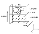
- FIG. 2 schematically shows the configuration of the thermoelectric conversion element according to the embodiment of the present invention.
- FIG. 3 is a conceptual diagram for explaining the principle of the thermoelectric conversion element according to the embodiment of the present invention.
- FIG. 4 shows measurement results of characteristics of an example of the thermoelectric conversion element according to the embodiment of the present invention.
- thermoelectric conversion element 1-1 Basic Configuration
- FIG. 2 schematically shows a spin-flow thermoelectric conversion element 1 according to an embodiment of the present invention.
- the spin current thermoelectric conversion element 1 includes a magnetic layer 2, an electromotive layer 3, and a power extraction terminal 5 as a basic configuration.
- the magnetic layer 2 has a magnetization component in the in-plane direction.
- the magnetic layer 2 is made of a material that exhibits a spin Seebeck effect, and generates a spin current by applying a temperature gradient.
- the material of the magnetic layer 2 may be a ferromagnetic metal or a magnetic insulator. Examples of the ferromagnetic metal include NiFe, CoFe, and CoFeB.
- magnetic insulators examples include yttrium iron garnet (YIG, Y3Fe5O12), bismuth (Bi) doped YIG (Bi: YIG), lanthanum (La) added YIG (LaY2Fe5O12), yttrium gallium iron garnet (Y3Fe5-xGaxO12). Etc. From the viewpoint of suppressing heat conduction by electrons, it is desirable to use a magnetic insulator.
- the electromotive layer 3 converts the generated spin current into electromotive force.
- the electromotive layer 3 is formed of a material that exhibits an inverse spin Hall effect (spin orbit interaction). More specifically, the material of the electromotive layer 3 contains a metal material having a large spin orbit interaction. For example, Au, Pt, Pd, Ir having a relatively large spin orbit interaction, a transition metal having d or f orbit, or an alloy material containing them is used. Further, the same effect can be obtained by simply doping a general metal film material such as Cu with a material such as Au, Pt, Pd, or Ir by about 0.5 to 10%.
- the electromotive layer 3 may be an oxide such as ITO or a semiconductor. From the viewpoint of efficiency, it is desirable to set the thickness of the electromotive layer 3 to about “spin diffusion length (spin relaxation length)” depending on the material. For example, when the electromotive layer 3 is a Pt film, the thickness is preferably set to about 10 to 30 nm.
- the power extraction terminal 5 is provided for extracting the electromotive force generated in the electromotive layer 3.
- FIG. 3 is a schematic diagram for explaining thermal spin current-electromotive force conversion in the spin current thermoelectric conversion element 1 having the basic configuration as described above.
- the magnetic layer 2 has a magnetization M in the x direction.
- the electromotive layer 3 is formed on the magnetic layer 2.
- a temperature gradient in the perpendicular direction (z direction) is applied to the laminated structure of the magnetic layer 2 and the electromotive layer 3.
- a spin current is generated through the interaction between the spins of the magnetic layer 2, and the conduction electrons of the electromotive layer 3 receive the spin angular momentum at the interface between the magnetic layer 2 and the electromotive layer 3.
- Spin injection occurs in the form of passing.
- the spin current thermoelectric conversion element 1 In order to suppress such a decrease in spin injection efficiency, the spin current thermoelectric conversion element 1 according to the present embodiment is further provided with a “spin injection layer 4” (see FIG. 2).
- the spin injection layer 4 As shown in FIG. 2, the spin injection layer 4 is provided as an interface for improving the spin injection efficiency from the magnetic layer 2 to the electromotive layer 3. Therefore, the spin injection layer 4 is formed between the magnetic layer 2 and the electromotive layer 3.
- the spin injection layer 4 is typically formed so as to be in contact with both the magnetic layer 2 and the electromotive layer 3, but is not limited thereto.
- the spin injection layer 4 is formed so as to be magnetically coupled to both the magnetic layer 2 and the electromotive layer 3.
- the state of being magnetically coupled means a state in which propagation of spin angular momentum occurs. Propagation of spin angular momentum is caused by the following factors: (1) Propagation due to the movement of spin-polarized conduction electrons and holes, (2) Pure spin current (mediated by movement of conduction electrons and holes with spin) (3) Propagation of spin waves or magnons caused by interaction between spins, propagation of spin density waves, etc. Therefore, in order to realize a magnetically coupled state, the spin injection layer 4, the magnetic layer 2, and the electromotive layer 3 do not necessarily have to be in contact with each other. As long as tunneling of spin carriers beyond the barrier and spin-spin interaction are realized, the spin injection layer 4, the magnetic layer 2, and the electromotive layer 3 may be somewhat separated from each other.
- the characteristics of the spin injection layer 4 are as follows. As described above, in the pure spin flow injected into the electromotive layer 3, the flow due to the up spin and the flow due to the down spin are in opposite directions, but the absolute amount is the same. If the localized spin is largely polarized on the side responsible for spin injection, the substantial spin injection efficiency is limited by the amount of spin in the direction of small amount. Therefore, for example, it is conceivable to use “antiferromagnetic material” having the same amount of upspin and downspin as the spin injection layer 4. As a result, it is possible to suppress a decrease in injection efficiency of the pure spin current into the electromotive layer 3.
- the up spin and the down spin are not necessarily present in the spin injection layer 4 in the same amount. It is also possible to use a “ferrimagnetic material” having an asymmetric amount of upspin and downspin and having a net magnetic moment (magnetization) as the spin injection layer 4. However, in order to improve the spin injection efficiency as compared with the case of a simple magnetic layer 2 / electromotive layer 3 stacked structure, the magnetic moment per unit volume (unit cell) is It is desirable that this is smaller than the magnetic layer 2.
- Nonmagnetic material having almost no spin for the spin injection layer 4.
- the absolute amount of spin contacting the magnetic body / electromotive body interface of the spin current thermoelectric conversion element that is, the spin of the spin that does not consider the direction (sign) It can be said that a larger amount is preferable. Therefore, it can be said that it is preferable that the spin injection layer 4 has a larger absolute amount of spin as well.
- At least one of the up spin density and the down spin density of the spin injection layer 4 is larger than the corresponding spin density of the magnetic layer 2.
- the material of the spin injection layer 4 include the following: transition metal or rare earth element having d orbit or f orbit in the outer shell, alloy material containing them, transition metal or rare earth element at least One kind of oxide, carbide, nitride, etc.
- transition metal or rare earth element having d orbit or f orbit in the outer shell
- alloy material containing them transition metal or rare earth element at least One kind of oxide, carbide, nitride, etc.
- manganese, chromium, an alloy of manganese and iridium (such as Mn80Ir20), an oxide containing manganese, iron, cobalt, or nickel called ferrite can be used.
- the spin injection layer 4 may be formed of an insulating material. In this case, it is possible to prevent a current generated in the electromotive layer 3 from flowing into the magnetic layer 2 and taking out the power. That is, it is preferable that substantial reduction in electromotive force conversion efficiency is prevented.
- the spin injection thermoelectric conversion element 1 is provided with the spin injection layer 4.
- the magnetic moment per unit volume of the spin injection layer 4 is smaller than the magnetic moment per unit volume of the magnetic layer 2.
- an antiferromagnetic material can be used, or a ferrimagnetic material having a net magnetic moment can be used.
- the magnetic layer 2 can be formed by sputtering, organometallic decomposition method (MOD method), sol-gel method, aerosol deposition method (AD method), ferrite plating method, liquid phase epitaxy method, solid phase epitaxy method, gas phase Examples include an epitaxy method, a dip method, a spray method, a spin coating method, and a printing method. In these cases, the magnetic layer 2 is formed on a support. In addition, as a method of forming the magnetic layer 2, a crystal pulling method, a magnetic insulator fiber manufacturing method using a drawing furnace, a sintering method, a melting method, and the like are also possible. In these cases, the bulk magnetic layer 2 is formed.
- MOD method organometallic decomposition method
- AD method aerosol deposition method
- ferrite plating method liquid phase epitaxy method
- liquid phase epitaxy method solid phase epitaxy method
- gas phase Examples include an epitaxy method, a dip method, a spray method, a spin coating method,
- the spin injection layer 4 can be formed by sputtering, organometallic decomposition (MOD), sol-gel, aerosol deposition (AD), ferrite plating, liquid phase epitaxy, solid phase epitaxy, vapor phase Examples include an epitaxy method, a dip method, a spray method, a spin coating method, and a printing method. Note that the thickness of the spin injection layer 4 is not particularly limited as long as the magnetic moment can be made smaller than that of the magnetic layer 2.
- Examples of the method for forming the electromotive layer 3 include a sputtering method, a vapor deposition method, a plating method, a screen printing method, an ink jet method, a spray method, and a spin coating method. In addition, coating / sintering of a nanocolloid solution can be used.
- the film thickness of the electromotive layer 3 is preferably set to at least the spin diffusion length (depth at which the spin current penetrates into the electromotive layer 3). For example, it is preferable to set 50 nm or more for Au and 10 nm or more for Pt. However, it is not necessary to unnecessarily thicken the electromotive layer 3 from the viewpoint of cost.
- the power extraction terminal 5 can be appropriately formed using existing mounting technology. There are at least two power extraction terminals 5. These power extraction terminals 5 are preferably arranged so that the electromotive force generated in the electromotive layer 3 can be extracted to the maximum.
- the order in which the magnetic layer 2, the spin injection layer 4, the electromotive layer 3, and the power extraction terminal 5 are produced is arbitrary.
- the magnetic layer 2, the spin injection layer 4, the electromotive layer 3, and the power extraction terminal 5 can be manufactured in this order, or vice versa.
- the spin injection layer 4 can be formed after the magnetic layer 2 and the electromotive layer 3 are continuously formed.
- the spin-flow thermoelectric conversion element 1 was fabricated on a gadolinium gallium garnet (GGG) crystalline substrate having a thickness of 700 ⁇ m.
- GGG gadolinium gallium garnet
- a bismuth-substituted yttrium iron garnet (Bi: YIG, composition is BiY 2 Fe 5 O 12 ) film was formed.
- the Bi: YIG film was formed by an organometallic decomposition method (MOD method).
- MOD method organometallic decomposition method
- a MOD solution manufactured by High Purity Chemical Laboratory Co., Ltd. was used.
- the evaluation element was produced by cutting the substrate into 2 ⁇ 8 mm strips. And the thermoelectric conversion performance was measured by using the element for evaluation.
- FIG. 4 shows the measurement results.
- a temperature difference of 7.9 K was applied in the entire thickness direction including the substrate.
- an external magnetic field was applied, and the state in which the output voltage was inverted according to the magnetization reversal of the element was measured.
- the spin Seebeck coefficient of this element was calculated using the value when the output voltage was saturated.
- Second Example a substrate in which 20 nm of thermally oxidized silicon was formed on a 450 ⁇ m thick silicon substrate was used.
- the magnetic layer 2 and the electromotive layer 3 are the same as in the case of the first example.
- the spin injection layer 4 is as follows. That is, a solution of iron chloride or nickel chloride was spin-coated on the YIG film at 3000 rpm for 1 minute. The concentration of iron chloride or nickel chloride at this time is as shown in Table 1. Thereafter, treatment was performed for 5 minutes under oxygen plasma generated at an oxygen partial pressure of 50 Pa and an RF output of 300 W. The iron chloride film or nickel chloride film after the oxygen plasma treatment is almost changed to iron oxide or nickel oxide, and it is expected that a small amount of chlorine is present as impurities on the surface. Although the detailed film thickness of iron oxide or nickel oxide is unknown, it is probably a very thin film of 1 nm or less.
- thermoelectric conversion performance was measured.
- Table 1 shows the measurement results. It was confirmed that the spin Seebeck coefficient was increased by introducing the spin injection layer 4 of this example. The rate of increase was a maximum of 51%.
- a Bi: YIG film having a thickness of 65 nm is formed as a magnetic layer 2 on a gadolinium gallium garnet (GGG) crystalline substrate having a thickness of 700 ⁇ m. Been formed.
- GGG gadolinium gallium garnet
- Ni film was deposited as a precursor of the spin injection layer 4, and then a 10 nm Pt film was deposited as the electromotive layer 3. Then, the baking process was performed for 5 minutes in the air heated at 600 degree
- a magnetic layer having a magnetization component in the in-plane direction A magnetic layer having a magnetization component in the in-plane direction;
- An electromotive layer comprising a material having a spin-orbit interaction;
- a spin injection layer provided between the magnetic layer and the electromotive layer, and magnetically coupled to both the magnetic layer and the electromotive layer;
- a thermoelectric conversion element wherein a magnetic moment per unit volume of the spin injection layer is smaller than a magnetic moment per unit volume of the magnetic layer.
- thermoelectric conversion element (Appendix 2) The thermoelectric conversion element according to attachment 1, wherein The thermoelectric conversion element, wherein the spin injection layer is an antiferromagnetic material.
- thermoelectric conversion element (Appendix 3) The thermoelectric conversion element according to attachment 1, wherein The spin injection layer is a ferrimagnetic material, Thermoelectric conversion element.
- thermoelectric conversion element (Appendix 4) The thermoelectric conversion element according to any one of appendices 1 to 3, A thermoelectric conversion element in which at least one of an up spin density and a down spin density of the spin injection layer is larger than a corresponding spin density of the magnetic layer.
- thermoelectric conversion element (Appendix 5) The thermoelectric conversion element according to any one of appendices 1 to 4,
- the magnetic layer is a ferromagnetic metal,
- thermoelectric conversion element, wherein the spin injection layer is an insulator.
- thermoelectric conversion element Forming a magnetic layer having a magnetization component in an in-plane direction; Forming an electromotive layer comprising a material having a spin orbit interaction; Forming a spin injection layer, and The spin injection layer is formed between the magnetic layer and the electromotive layer, and is magnetically coupled to both the magnetic layer and the electromotive layer, The method of manufacturing a thermoelectric conversion element, wherein a magnetic moment per unit volume of the spin injection layer is smaller than a magnetic moment per unit volume of the magnetic layer.
Landscapes
- Engineering & Computer Science (AREA)
- Manufacturing & Machinery (AREA)
- Hall/Mr Elements (AREA)
Description
effect)」と呼ばれている。また、その逆の現象として、スピン流が流れると起電力が発生することも知られている。これは、「逆スピンホール効果(inverse spin-Hall effect)」と呼ばれている。逆スピンホール効果を利用することによって、スピン流を検出することができる。尚、スピンホール効果も逆スピンホール効果も、「スピン軌道相互作用(spin orbit coupling)」が大きな物質(例:Pt、Pd)において有意に発現する。
1-1.基本構成
図2は、本発明の実施の形態に係るスピン流熱電変換素子1を概略的に示している。スピン流熱電変換素子1は、基本構成として、磁性体層2、起電体層3、及び電力取り出し端子5を備えている。
図2に示されるように、スピン注入層4は、磁性体層2から起電体層3へのスピン注入効率を向上させるためのインターフェースとして設けられている。そのために、スピン注入層4は、磁性体層2と起電体層3との間に形成されている。スピン注入層4は、典型的には、磁性体層2と起電体層3の両方に接触するように形成されるが、それに限られない。
次に、本実施の形態に係るスピン流熱電変換素子1の製造方法を説明する。
次に、本実施の形態の具体例を、説明する。
第1の例では、厚さ700μmのガドリニウムガリウムガーネット(GGG)の結晶性基板上に、スピン流熱電変換素子1を作製した。
第2の例では、厚さ450μmのシリコン基板上に20nmの熱酸化シリコンを形成した基板を用いた。磁性体層2及び起電体層3は、上記第1の例の場合と同様である。

第3の例では、上記第1の例と同様に、厚さ700μmのガドリニウムガリウムガーネット(GGG)の結晶性基板上に、厚さ65nmのBi:YIG膜が磁性体層2として形成された。
面内方向の磁化成分を有する磁性体層と、
スピン軌道相互作用を有する材料を含む起電体層と、
前記磁性体層と前記起電体層との間に設けられ、前記磁性体層と前記起電体層の両方に磁気的に結合するスピン注入層と
を備え、
前記スピン注入層の単位体積当たりの磁気モーメントは、前記磁性体層の単位体積当たりの磁気モーメントよりも小さい
熱電変換素子。
付記1に記載の熱電変換素子であって、
前記スピン注入層は、反強磁性体である
熱電変換素子。
付記1に記載の熱電変換素子であって、
前記スピン注入層は、フェリ磁性体であり、
熱電変換素子。
付記1乃至3のいずれか一項に記載の熱電変換素子であって、
前記スピン注入層のアップスピン密度とダウンスピン密度の少なくとも一方が、前記磁性体層の対応するスピン密度よりも大きい
熱電変換素子。
付記1乃至4のいずれか一項に記載の熱電変換素子であって、
前記磁性体層は、強磁性金属であり、
前記スピン注入層は、絶縁体である
熱電変換素子。
面内方向の磁化成分を有する磁性体層を形成するステップと、
スピン軌道相互作用を有する材料を含む起電体層を形成するステップと、
スピン注入層を形成するステップと
を含み、
前記スピン注入層は、前記磁性体層と前記起電体層との間に形成され、前記磁性体層と前記起電体層の両方に磁気的に結合し、
前記スピン注入層の単位体積当たりの磁気モーメントは、前記磁性体層の単位体積当たりの磁気モーメントよりも小さい
熱電変換素子の製造方法。
Claims (6)
- 面内方向の磁化成分を有する磁性体層と、
スピン軌道相互作用を有する材料を含む起電体層と、
前記磁性体層と前記起電体層との間に設けられ、前記磁性体層と前記起電体層の両方に磁気的に結合するスピン注入層と
を備え、
前記スピン注入層の単位体積当たりの磁気モーメントは、前記磁性体層の単位体積当たりの磁気モーメントよりも小さい
熱電変換素子。 - 請求項1に記載の熱電変換素子であって、
前記スピン注入層は、反強磁性体である
熱電変換素子。 - 請求項1に記載の熱電変換素子であって、
前記スピン注入層は、フェリ磁性体であり、
熱電変換素子。 - 請求項1乃至3のいずれか一項に記載の熱電変換素子であって、
前記スピン注入層のアップスピン密度とダウンスピン密度の少なくとも一方が、前記磁性体層の対応するスピン密度よりも大きい
熱電変換素子。 - 請求項1乃至4のいずれか一項に記載の熱電変換素子であって、
前記磁性体層は、強磁性金属であり、
前記スピン注入層は、絶縁体である
熱電変換素子。 - 面内方向の磁化成分を有する磁性体層を形成するステップと、
スピン軌道相互作用を有する材料を含む起電体層を形成するステップと、
スピン注入層を形成するステップと
を含み、
前記スピン注入層は、前記磁性体層と前記起電体層との間に形成され、前記磁性体層と前記起電体層の両方に磁気的に結合し、
前記スピン注入層の単位体積当たりの磁気モーメントは、前記磁性体層の単位体積当たりの磁気モーメントよりも小さい
熱電変換素子の製造方法。
Priority Applications (2)
| Application Number | Priority Date | Filing Date | Title |
|---|---|---|---|
| JP2014535391A JP6233311B2 (ja) | 2012-09-12 | 2013-04-15 | 熱電変換素子及びその製造方法 |
| US14/425,188 US9306153B2 (en) | 2012-09-12 | 2013-04-15 | Thermoelectric conversion element and method for manufacturing the same |
Applications Claiming Priority (2)
| Application Number | Priority Date | Filing Date | Title |
|---|---|---|---|
| JP2012200535 | 2012-09-12 | ||
| JP2012-200535 | 2012-09-12 |
Publications (1)
| Publication Number | Publication Date |
|---|---|
| WO2014041838A1 true WO2014041838A1 (ja) | 2014-03-20 |
Family
ID=50277976
Family Applications (1)
| Application Number | Title | Priority Date | Filing Date |
|---|---|---|---|
| PCT/JP2013/061225 Ceased WO2014041838A1 (ja) | 2012-09-12 | 2013-04-15 | 熱電変換素子及びその製造方法 |
Country Status (3)
| Country | Link |
|---|---|
| US (1) | US9306153B2 (ja) |
| JP (1) | JP6233311B2 (ja) |
| WO (1) | WO2014041838A1 (ja) |
Cited By (1)
| Publication number | Priority date | Publication date | Assignee | Title |
|---|---|---|---|---|
| JP2016162881A (ja) * | 2015-03-02 | 2016-09-05 | 日本電気株式会社 | 熱電変換素子とその製造方法 |
Families Citing this family (3)
| Publication number | Priority date | Publication date | Assignee | Title |
|---|---|---|---|---|
| JP2018049676A (ja) | 2016-09-23 | 2018-03-29 | 株式会社東芝 | 高周波アシスト磁気記録ヘッド、磁気ヘッドアセンブリ、及び磁気記録再生装置 |
| US10516098B2 (en) * | 2016-12-22 | 2019-12-24 | Purdue Research Foundation | Apparatus for spin injection enhancement and method of making the same |
| JP2020035971A (ja) * | 2018-08-31 | 2020-03-05 | Tdk株式会社 | スピン流磁化回転型磁気素子、スピン流磁化回転型磁気抵抗効果素子及び磁気メモリ |
Citations (1)
| Publication number | Priority date | Publication date | Assignee | Title |
|---|---|---|---|---|
| JP2009130070A (ja) * | 2007-11-22 | 2009-06-11 | Keio Gijuku | スピン流熱変換素子及び熱電変換素子 |
Family Cites Families (4)
| Publication number | Priority date | Publication date | Assignee | Title |
|---|---|---|---|---|
| CN103718302A (zh) * | 2011-05-23 | 2014-04-09 | 日本电气株式会社 | 热电转换元件和热电转换方法 |
| US9947855B2 (en) * | 2011-09-26 | 2018-04-17 | Nec Corporation | Thermoelectric conversion element and method of manufacturing the same, and heat radiation fin |
| JP6066091B2 (ja) * | 2011-09-27 | 2017-01-25 | 日本電気株式会社 | 熱電変換素子及びその製造方法 |
| US9859486B2 (en) * | 2012-07-19 | 2018-01-02 | Nec Corporation | Thermoelectric conversion element and manufacturing method for same |
-
2013
- 2013-04-15 US US14/425,188 patent/US9306153B2/en active Active
- 2013-04-15 WO PCT/JP2013/061225 patent/WO2014041838A1/ja not_active Ceased
- 2013-04-15 JP JP2014535391A patent/JP6233311B2/ja active Active
Patent Citations (1)
| Publication number | Priority date | Publication date | Assignee | Title |
|---|---|---|---|---|
| JP2009130070A (ja) * | 2007-11-22 | 2009-06-11 | Keio Gijuku | スピン流熱変換素子及び熱電変換素子 |
Non-Patent Citations (1)
| Title |
|---|
| UCHIDA ET AL.: "Electric detection of the spin-Seebeck effect in magnetic insulator in the presence of interface barrier", JOURNAL OF PHYSICS: CONFERENCE SERIES, vol. 303, no. ISSUE, July 2011 (2011-07-01), pages 012096 * |
Cited By (1)
| Publication number | Priority date | Publication date | Assignee | Title |
|---|---|---|---|---|
| JP2016162881A (ja) * | 2015-03-02 | 2016-09-05 | 日本電気株式会社 | 熱電変換素子とその製造方法 |
Also Published As
| Publication number | Publication date |
|---|---|
| JPWO2014041838A1 (ja) | 2016-08-18 |
| US20150236246A1 (en) | 2015-08-20 |
| JP6233311B2 (ja) | 2017-11-22 |
| US9306153B2 (en) | 2016-04-05 |
Similar Documents
| Publication | Publication Date | Title |
|---|---|---|
| Zheng et al. | High‐Efficiency Magnon‐Mediated Magnetization Switching in All‐Oxide Heterostructures with Perpendicular Magnetic Anisotropy | |
| JP5585314B2 (ja) | 熱電変換素子及び熱電変換装置 | |
| JP5991589B2 (ja) | 熱電変換素子、熱電変換素子の製造方法および熱電変換方法 | |
| JP6233320B2 (ja) | 熱電変換素子及びその製造方法 | |
| Li et al. | Thermally stable voltage-controlled perpendicular magnetic anisotropy in Mo| CoFeB| MgO structures | |
| Vaz et al. | Oxide spin-orbitronics: New routes towards low-power electrical control of magnetization in oxide heterostructures | |
| WO2009151000A1 (ja) | 熱電変換素子 | |
| Lan et al. | Giant tunneling magnetoresistance in spin-filter magnetic tunnel junctions based on van der Waals A-type antiferromagnet CrSBr | |
| Zhang et al. | Magnetic two-dimensional van der Waals materials for spintronic devices | |
| JP7669069B2 (ja) | 熱電体、熱電発電素子、多層熱電体、多層熱電発電素子、熱電発電機、及び熱流センサ | |
| JP6233311B2 (ja) | 熱電変換素子及びその製造方法 | |
| Lv et al. | Enhancement of spin–orbit torque in WTe2/perpendicular magnetic anisotropy heterostructures | |
| JPWO2017082266A1 (ja) | 熱電変換素子用起電膜及び熱電変換素子 | |
| JP2014072250A (ja) | 熱電変換素子及びその製造方法 | |
| Zheng et al. | Enhanced torque efficiency in ferromagnetic multilayers by introducing naturally oxidized Cu | |
| JP6066091B2 (ja) | 熱電変換素子及びその製造方法 | |
| Li et al. | Field-free magnetization switching with full scale in Pt/Tm3Fe5O12 bilayer on vicinal substrate | |
| Gao et al. | Surface half-metallicity of CrS thin films and perfect spin filtering and spin diode effects of CrS/ZnSe heterostructure | |
| JP6349863B2 (ja) | スピン流熱電変換素子とその製造方法および熱電変換装置 | |
| WO2013047253A1 (ja) | 熱電変換素子及びその製造方法 | |
| Zhao et al. | Strong magnetoelectric coupling in Tb–Fe∕ Pb (Zr0. 52Ti0. 48) O3 thin-film heterostructure prepared by low energy cluster beam deposition | |
| JP6172439B2 (ja) | スピン流熱電変換素子 | |
| Zhao et al. | Magnon-mediated switching of perpendicular magnetization by the topological crystalline insulator SnTe with high spin Hall conductivity | |
| JP6191620B2 (ja) | 熱電変換素子及びその製造方法 | |
| JP6225167B2 (ja) | 保護層を中心に有するスピン注入デバイス |
Legal Events
| Date | Code | Title | Description |
|---|---|---|---|
| 121 | Ep: the epo has been informed by wipo that ep was designated in this application |
Ref document number: 13836292 Country of ref document: EP Kind code of ref document: A1 |
|
| WWE | Wipo information: entry into national phase |
Ref document number: 14425188 Country of ref document: US |
|
| ENP | Entry into the national phase |
Ref document number: 2014535391 Country of ref document: JP Kind code of ref document: A |
|
| NENP | Non-entry into the national phase |
Ref country code: DE |
|
| 122 | Ep: pct application non-entry in european phase |
Ref document number: 13836292 Country of ref document: EP Kind code of ref document: A1 |