WO2014041648A1 - 半導体装置 - Google Patents
半導体装置 Download PDFInfo
- Publication number
- WO2014041648A1 WO2014041648A1 PCT/JP2012/073382 JP2012073382W WO2014041648A1 WO 2014041648 A1 WO2014041648 A1 WO 2014041648A1 JP 2012073382 W JP2012073382 W JP 2012073382W WO 2014041648 A1 WO2014041648 A1 WO 2014041648A1
- Authority
- WO
- WIPO (PCT)
- Prior art keywords
- chip
- temperature sensor
- semiconductor device
- heater
- gas
- Prior art date
- Legal status (The legal status is an assumption and is not a legal conclusion. Google has not performed a legal analysis and makes no representation as to the accuracy of the status listed.)
- Ceased
Links
Images














Classifications
-
- G—PHYSICS
- G01—MEASURING; TESTING
- G01P—MEASURING LINEAR OR ANGULAR SPEED, ACCELERATION, DECELERATION, OR SHOCK; INDICATING PRESENCE, ABSENCE, OR DIRECTION, OF MOVEMENT
- G01P15/00—Measuring acceleration; Measuring deceleration; Measuring shock, i.e. sudden change of acceleration
- G01P15/006—Measuring acceleration; Measuring deceleration; Measuring shock, i.e. sudden change of acceleration by making use of fluid seismic masses
- G01P15/008—Measuring acceleration; Measuring deceleration; Measuring shock, i.e. sudden change of acceleration by making use of fluid seismic masses by using thermal pick-up
-
- G—PHYSICS
- G01—MEASURING; TESTING
- G01P—MEASURING LINEAR OR ANGULAR SPEED, ACCELERATION, DECELERATION, OR SHOCK; INDICATING PRESENCE, ABSENCE, OR DIRECTION, OF MOVEMENT
- G01P15/00—Measuring acceleration; Measuring deceleration; Measuring shock, i.e. sudden change of acceleration
- G01P15/02—Measuring acceleration; Measuring deceleration; Measuring shock, i.e. sudden change of acceleration by making use of inertia forces using solid seismic masses
- G01P15/08—Measuring acceleration; Measuring deceleration; Measuring shock, i.e. sudden change of acceleration by making use of inertia forces using solid seismic masses with conversion into electric or magnetic values
- G01P15/0897—Measuring acceleration; Measuring deceleration; Measuring shock, i.e. sudden change of acceleration by making use of inertia forces using solid seismic masses with conversion into electric or magnetic values by thermal pick-up
Definitions
- the present invention relates to a semiconductor device, and more particularly to a semiconductor device equipped with a gas type acceleration sensor.
- acceleration sensors have been widely used in portable information devices such as smartphones, tablet PCs, and portable game machines.
- a capacitance type for example, see Patent Document 1
- a piezoresistive type for example, see Patent Document 2
- a gas type for example, see Patent Document 3, Patent Document 4, and Patent Document 5. It has been known.
- the electrostatic capacitance type and the piezoresistive type are acceleration sensors using MEMS (Micro-Electro Mechanical Systems) elements. More specifically, a “mechanically movable part” is formed in a semiconductor chip by using a MEMS element. The movement of the movable part due to the acceleration of the semiconductor chip is detected through a capacitance change or a piezoelectric element. However, it is not preferable from the viewpoint of manufacturing cost that a mechanically movable part must be formed, resulting in a decrease in yield.
- MEMS Micro-Electro Mechanical Systems
- a heater and a temperature sensor are provided in a space in the semiconductor chip, and further, gas is sealed in the space. Due to the acceleration of the semiconductor chip, the gas in the space moves and the temperature distribution of the gas changes. By detecting the change in the temperature distribution with a temperature sensor, the acceleration of the semiconductor chip is detected. In the case of this gas type acceleration sensor, the “mechanical movable part” is unnecessary, which is preferable from the viewpoint of yield and manufacturing cost.
- Patent Document 6 discloses a method of mounting an entire acceleration sensor package perpendicular to a printed circuit board.
- Patent Document 7 discloses a system in which a magnetic sensor is arranged on a tapered substrate.
- a gas-type acceleration sensor that can detect accelerations in a plurality of directions and is configured in a more advantageous form from the viewpoint of configuration and manufacturing is desired.
- a semiconductor device in one embodiment, includes a gas-type acceleration sensor including a heater, a first temperature sensor, and a second temperature sensor as components.
- the semiconductor device further includes a first chip in which the heater is formed on the first surface among the components, and a second chip in which the first temperature sensor and the second temperature sensor are formed on the second surface among the components.
- a connecting member for electrically connecting the first chip and the second chip.
- the first chip and the second chip are stacked via a connection member so that the first surface and the second surface face each other. In the stacking direction of the first chip and the second chip, the position of the heater is different from the positions of the first temperature sensor and the second temperature sensor.
- the first temperature sensor and the second temperature sensor are arranged to face each other with the heater interposed therebetween.
- One of the first chip and the second chip is a base chip, and the other of the first chip and the second chip is a cap chip stacked on the base chip.
- the components of the gas acceleration sensor formed on the cap chip are in direct contact with the connection member.
- a method for manufacturing a semiconductor device includes a gas-type acceleration sensor including a heater, a first temperature sensor, and a second temperature sensor as components.
- the manufacturing method includes: (A) a step of forming a heater among the components on the first surface of the first chip; and (B) a first temperature sensor among the components on the second surface of the second chip. Forming a second temperature sensor; and (C) flip-connecting the first chip and the second chip via a connecting member so that the first surface and the second surface face each other. In the stacking direction of the first chip and the second chip, the position of the heater is different from the positions of the first temperature sensor and the second temperature sensor.
- the first temperature sensor and the second temperature sensor are arranged to face each other with the heater interposed therebetween.
- One of the first chip and the second chip is a base chip, and the other of the first chip and the second chip is a cap chip stacked on the base chip.
- the components of the gas acceleration sensor formed on the cap chip are in direct contact with the connection member.
- a gas type acceleration sensor configured in a more advantageous form from the viewpoint of configuration and manufacturing is realized.
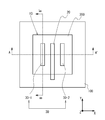
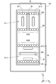
- FIG. 1 is a plan view conceptually showing the structure of the semiconductor device according to the first embodiment.
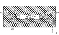
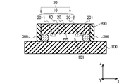
- FIG. 2A conceptually shows a cross-sectional structure taken along line A-A ′ in FIG.
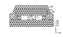
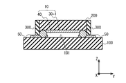
- FIG. 2B conceptually shows a cross-sectional structure taken along line B-B ′ in FIG.
- FIG. 2C is a conceptual diagram showing an example of a planar arrangement of the semiconductor device according to the first exemplary embodiment.
- FIG. 3 is a diagram for explaining the operation of the semiconductor device according to the first embodiment.
- FIG. 4A is a diagram for explaining the operation of the semiconductor device according to the first embodiment.
- FIG. 4B is a diagram for explaining the operation of the semiconductor device according to the first embodiment.
- FIG. 5A is a diagram for explaining the operation of the semiconductor device according to the first embodiment.
- FIG. 5B is a diagram for explaining the operation of the semiconductor device according to the first embodiment.
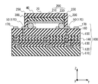
- FIG. 6 is a sectional view showing an example of the structure of the semiconductor device according to the first embodiment.
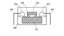
- FIG. 7 is a conceptual diagram showing an example of a package configuration of the semiconductor device according to the first embodiment.
- FIG. 8 is a conceptual diagram showing an example of a package configuration of the semiconductor device according to the first embodiment.
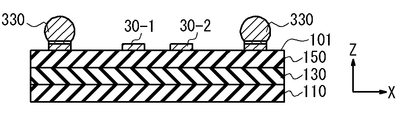
- FIG. 9A is a cross-sectional view illustrating an example of the method for manufacturing the semiconductor device according to the first embodiment.
- FIG. 9B is a cross-sectional view illustrating an example of the method for manufacturing the semiconductor device according to the first embodiment.
- FIG. 9C is a cross-sectional view illustrating an example of the method for manufacturing the semiconductor device according to the first embodiment.
- FIG. 9D is a cross-sectional view illustrating an example of the method for manufacturing the semiconductor device according to the first embodiment.
- FIG. 9E is a cross-sectional view showing an example of the method for manufacturing the semiconductor device according to the first embodiment.
- FIG. 9F is a cross-sectional view showing an example of the method for manufacturing the semiconductor device according to the first embodiment.
- FIG. 9G is a cross-sectional view illustrating an example of the method for manufacturing the semiconductor device according to the first embodiment.
- FIG. 9H is a cross-sectional view illustrating an example of the method for manufacturing the semiconductor device according to the first embodiment.
- FIG. 9I is a cross-sectional view illustrating an example of the method for manufacturing the semiconductor device according to the first embodiment.
- FIG. 9J is a cross-sectional view showing an example of the method for manufacturing the semiconductor device according to the first embodiment.
- FIG. 9K is a cross-sectional view illustrating an example of the method for manufacturing the semiconductor device according to the first embodiment.
- FIG. 9L is a cross-sectional view showing an example of the method for manufacturing the semiconductor device according to the first embodiment.
- FIG. 10A is a cross-sectional view illustrating another example of the method for manufacturing the semiconductor device according to the first embodiment.
- FIG. 10B is a cross-sectional view illustrating another example of the method for manufacturing the semiconductor device according to the first embodiment.
- FIG. 10C is a cross-sectional view showing another example of the method for manufacturing the semiconductor device according to the first embodiment.
- FIG. 10A is a cross-sectional view illustrating another example of the method for manufacturing the semiconductor device according to the first embodiment.
- FIG. 10B is a cross-sectional view illustrating another example of the method for manufacturing the semiconductor device according to the first embodiment.
- FIG. 10D is a cross-sectional view illustrating another example of the method for manufacturing the semiconductor device according to the first embodiment.
- FIG. 11 is a plan view conceptually showing the structure of the semiconductor device according to the second embodiment.
- FIG. 12A conceptually shows a cross-sectional structure taken along line A-A ′ in FIG.
- FIG. 12B conceptually shows a cross-sectional structure taken along line B-B ′ in FIG.
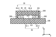
- FIG. 13 is a cross-sectional view conceptually showing the structure of the semiconductor device according to the third embodiment.
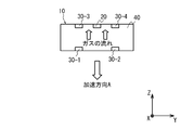
- FIG. 14 is a diagram for explaining the operation of the semiconductor device according to the third embodiment.
- FIG. 15 is a cross-sectional view conceptually showing the structure of the semiconductor device according to the fourth embodiment.
- FIG. 16 is a diagram for explaining the operation of the semiconductor device according to the fourth embodiment.
- FIG. 17 is a diagram for explaining the operation of the semiconductor device according to the fourth embodiment.
- FIG. 18 is a plan view conceptually showing the structure of the semiconductor device according to the fifth embodiment.
- FIG. 19 is a plan view conceptually showing the structure of the semiconductor device according to the fifth embodiment.
- FIG. 20 is a plan view conceptually showing the structure of the semiconductor device according to the sixth embodiment.
- FIG. 21 is a plan view conceptually showing the structure of the semiconductor device according to the sixth embodiment.
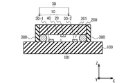
- FIG. 1 is a plan view conceptually showing the configuration of the semiconductor device according to the first embodiment.
- FIG. 2A conceptually shows a cross-sectional structure taken along line AA ′ in FIG.
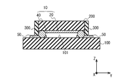
- FIG. 2B conceptually shows a cross-sectional structure taken along line BB ′ in FIG.
- the semiconductor device includes at least two semiconductor chips, and the semiconductor chips are stacked.
- the lower semiconductor chip is hereinafter referred to as “base chip 100”, and the upper chip is hereinafter referred to as “cap chip 200”.
- the cap chip 200 is stacked on the base chip 100. More specifically, the base chip 100 and the cap chip 200 are stacked so that the surface 101 of the base chip 100 and the surface 201 of the cap chip 200 face each other. That is, the base chip 100 and the cap chip 200 are flip-connected.
- connection member 300 is used for electrical connection between the base chip 100 and the cap chip 200.
- the connection member 300 is a bump (bump electrode).
- the connection member 300 not only electrically connects the base chip 100 and the cap chip 200 but also serves as a spacer that mechanically supports the cap chip 200. That is, the base chip 100 and the cap chip 200 are stacked via the connection member 300. In order to stably support the cap chip 200, it is sufficient that three or more connection members 300 are provided. In addition, some of the connection members 300 may be “dummy connection members” that do not actually contribute to electrical connection.
- the stacking direction of the base chip 100 and the cap chip 200 is referred to as the Z direction.
- In-plane directions orthogonal to the Z direction are the X direction and the Y direction.
- the X direction and the Y direction are orthogonal to each other.
- the semiconductor device includes a gas acceleration sensor 10.
- the gas acceleration sensor 10 detects the acceleration of the semiconductor device by detecting a change in the temperature distribution of the gas in the space 40. More specifically, the gas acceleration sensor 10 includes a heater 20, a first temperature sensor 30-1, and a second temperature sensor 30-2 as components.
- the heater 20 generates heat when energized.
- the heater 20 is formed of a metal wiring such as Al or Cu.
- the metal wiring as the heater 20 is formed so as to extend in the Y direction.
- the heater 20 is formed on the cap chip 200 side. More specifically, the heater 20 is formed on the surface 201 of the cap chip 200 and is exposed to the space 40.
- the first temperature sensor 30-1 and the second temperature sensor 30-2 are provided for measuring the temperature of the gas in the space 40.
- the space 40 is filled with an inert gas such as nitrogen, argon, or helium, or air.
- these temperature sensors 30 are also formed of metal wiring such as Al or Cu.
- the metal wiring as the temperature sensor 30 is formed so as to extend in the Y direction.
- the first temperature sensor 30-1 and the second temperature sensor 30-2 are formed on the base chip 100 side. More specifically, the first temperature sensor 30-1 and the second temperature sensor 30-2 are formed on the surface 101 of the base chip 100 and are exposed to the space 40.
- the first temperature sensor 30-1 and the second temperature sensor 30-2 are arranged on both sides of the heater 20 as a heat source.
- the first temperature sensor 30-1 and the second temperature sensor 30-2 are arranged to face each other with the heater 20 in between.
- the distance between the first temperature sensor 30-1 and the heater 20 is equal to the distance between the second temperature sensor 30-2 and the heater 20. That is, the first temperature sensor 30-1 and the second temperature sensor 30-2 are arranged at symmetrical positions with the heater 20 as the center.
- the position of the heater 20 is different from the positions of the first temperature sensor 30-1 and the second temperature sensor 30-2. This is because the heater 20 is formed on the surface 201 of the cap chip 200, while the first temperature sensor 30-1 and the second temperature sensor 30-2 are formed on the surface 101 of the base chip 100. It is.
- the heater 20 is in direct contact with the connection member 300 at two different points. More specifically, the pair of connection members 300 are provided apart from each other in the Y direction, and both ends of the heater 20 (metal wiring) are in direct contact with each of the pair of connection members 300.
- the pair of connection members 300 are in contact with the wiring 50 formed on the surface 101 of the base chip 100.
- the wiring 50 is electrically connected to elements formed in the base chip 100.
- the wiring 50 is not always necessary, and the connection member 300 may be in contact with an electrode pad formed on the surface 101 of the base chip 100.
- a current can be directly supplied from the base chip 100 through the connecting member 300 to the heater 20 formed on the cap chip 200 side.
- the fact that the heater 20 on the cap chip 200 side is in direct contact with the connection member 300 means that the heater 20 also serves as an electrode pad. In this case, there is no need to separately form an electrode pad on the surface 201 of the cap chip 200 or route the wiring inside the cap chip 200. Therefore, the manufacturing is easy and the manufacturing cost is reduced.
- FIG. 2C conceptually shows an example of a planar arrangement of the semiconductor device according to the present embodiment.
- a side fill 250 for example, polyimide
- the first temperature sensor 30-1, the second temperature sensor 30-2, and the wiring 50 are formed so as to protrude outside the side fill 250.
- the connection member 300 (bump) includes a bump that contacts the heater 20 and allows a current to flow, and a dummy bump that does not contribute to electrical connection. In order to stably support the cap chip 200, it is sufficient that three or more connection members 300 (bumps) are provided.
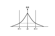
- FIG. 3 shows a temperature distribution in a state where the semiconductor device is not accelerated (for example, a stationary state).
- the vertical axis represents temperature
- the horizontal axis represents the position in the X direction. In this state, a symmetrical temperature distribution centering on the position of the heater 20 is formed.
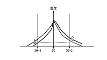
- FIG. 4A conceptually shows a state in which “acceleration in the ⁇ X direction” is applied to the semiconductor device.
- FIG. 4B shows the temperature distribution in the state shown in FIG. 4A.
- the gas in the space 40 cannot follow the movement of the semiconductor device. Therefore, in the space 40, a gas flow (relative movement) occurs in a direction (+ X direction) opposite to the acceleration direction A ( ⁇ X direction). Since hot gas flows in the + X direction in the space 40, the temperature distribution is also biased in the + X direction.
- the temperature increases at the position of the second temperature sensor 30-2, while the temperature decreases at the position of the first temperature sensor 30-1.
- the first temperature sensor 30-1 and the second temperature sensor 30-2 such a temperature change pattern can be detected. In other words, it is possible to detect “acceleration in the ⁇ X direction” from detection of such a temperature change pattern.
- the detected temperature change pattern is opposite to that shown in FIG. 4B. Accordingly, it is possible to distinguish between “acceleration in the ⁇ X direction” and “acceleration in the + X direction”.
- FIG. 5A conceptually shows a state in which “acceleration in the ⁇ Z direction” is applied to the semiconductor device.
- FIG. 5B shows the temperature distribution in the state shown in FIG. 5A.
- the gas in the space 40 cannot follow the movement of the semiconductor device. Therefore, in the space 40, a gas flow (relative movement) occurs in a direction (+ Z direction) opposite to the acceleration direction A ( ⁇ Z direction). Since hot gas flows in the + Z direction in the space 40, the temperature distribution is also biased in the + Z direction. As a result, the temperature decreases at the positions of both the first temperature sensor 30-1 and the second temperature sensor 30-2.
- the first temperature sensor 30-1 and the second temperature sensor 30-2 such a temperature change pattern can be detected.
- “acceleration in the ⁇ Z direction” can be detected from detection of such a temperature change pattern.
- the gas-type acceleration sensor 10 of the present embodiment it is possible to detect accelerations in two directions of the X direction and the Z direction with a simple configuration.
- the acceleration in the X direction can be detected because the first temperature sensor 30-1 and the second temperature sensor 30-2 are disposed on both sides of the heater 20 in the X direction.
- the acceleration in the Z direction can be detected because the position of the heater 20 is different from the positions of the first temperature sensor 30-1 and the second temperature sensor 30-2 in the Z direction.
- the heater 20 on the cap chip 200 side is in direct contact with the connection member 300.
- the heater 20 also serves as an electrode pad.
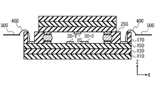
- FIG. 6 shows an example of the structure of the semiconductor device according to this embodiment.
- a transistor 120 is formed on a silicon substrate 110.
- An insulating film 130 is formed so as to cover the silicon substrate 110 and the transistor 120, and a multilayer wiring 140 connected to the transistor 120 is formed in the insulating film 130.
- an insulating film 150 is formed on the insulating film 130, and a via 160 connected to the multilayer wiring 140 is formed in the insulating film 150.
- an uppermost layer wiring 170 connected to the via 160 is formed on the insulating film 150.
- the uppermost layer wiring 170 includes a temperature sensor 30, a wiring 50, an electrode pad, and the like.
- the uppermost layer wiring 170 is made of, for example, Al.
- an insulating film 220 is formed on the silicon substrate 210.
- metal wiring eg, Al
- the number of insulating layers on the base chip 100 described above is larger than the total number of insulating layers on the cap chip 200.
- bumps are formed as connection members 300.
- the bump 300 not only electrically connects the base chip 100 and the cap chip 200 but also serves as a spacer that mechanically supports the cap chip 200.
- the heater 20 formed on the cap chip 200 side is in direct contact with the bump 300. That is, the heater 20 also serves as an electrode pad. A current can be directly supplied to the heater 20 via the bumps 300.
- a side fill 250 (eg, polyimide) is formed so as to surround the cap chip 200.
- a space 40 surrounded by the base chip 100, the cap chip 200 and the side fill 250 is formed. Gas is sealed in the space 40.
- the gas acceleration sensor 10 detects the acceleration of the semiconductor device by detecting a change in the temperature distribution of the gas in the space 40.
- the transistor 120 is formed in the base chip 100, but no transistor is formed in the cap chip 200. This is because the heater 20 is in direct contact with the bump 300 and ON / OFF of the heater 20 can be controlled from the base chip 100 side. In the cap chip 200, it is not necessary to form a transistor for controlling ON / OFF of the heater 20 or a multilayer wiring. Therefore, the manufacturing cost is reduced.
- the quality of the silicon substrate 210 of the cap chip 200 may be lower than the quality of the silicon substrate 110 of the base chip 100 on which the transistor 120 is formed. This also contributes to a reduction in manufacturing cost.
- defect density One index of silicon substrate (semiconductor substrate) quality is “defect density”.
- the defect density of the silicon substrate 210 of the cap chip 200 may be higher than the defect density of the silicon substrate 110 of the base chip 100.
- a light scattering method is generally used as a method for measuring defects on the surface of the substrate (wafer). According to the light scattering method, the surface of a substrate (wafer) is irradiated with a convergent laser beam having a wavelength of 400 to 700 nm. And the scattered light in a defective part is detected with a light receiving element. The defect density can be obtained based on the detection frequency, detection state, etc. of the scattered light.
- the heater 20 which is a heat source is formed on the upper cap chip 200.
- the heater 20 which is a heat source is formed on the upper cap chip 200.
- heat radiation from the uppermost silicon substrate 210 can be expected.
- the position of the heater 20 is far from the transistor 120 formed in the base chip 100, the influence of the heat of the heater 20 on the operation of the transistor 120 can be suppressed.
- Electrode pads (a part of the uppermost layer wiring 170) on the surface of the base chip 100 are connected to the leads 500 through bonding wires 400. Further, the semiconductor device is sealed with the mold resin 600.
- FIGS. 9A to 9L are cross-sectional views showing an example of a manufacturing method of the semiconductor device according to the present embodiment.
- a laminated structure of the silicon substrate 110, the insulating film 130, and the insulating film 150 of the base chip 100 is formed.
- the transistor 120 (not shown) is formed on the silicon substrate 110.
- a multilayer wiring 140 (not shown) is formed in the insulating film 130.
- a via 160 (not shown) is formed in the insulating film 150.
- the uppermost layer wiring 170 is formed on the surface of the insulating film 150.
- the uppermost layer wiring 170 includes a temperature sensor 30, a wiring 50, an electrode pad, and the like.
- the uppermost layer wiring 170 is made of, for example, Al.
- a resist film 310 is formed so as to cover the insulating film 150 and the uppermost layer wiring 170. Furthermore, an opening is formed at a position where the bump 300 is formed later.
- a Cu plating layer 180 is formed on the uppermost wiring 170 in the opening.
- solder 320 is formed so as to fill the opening.
- the solder 320 is, for example, an Sn alloy.
- the resist film 310 is removed.
- solder reflow is performed.
- solder reflow is performed.
- the spherical solder 330 is formed.
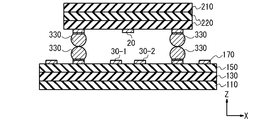
- the cap chip 200 is also formed in the same manner as the base chip 100 described above. As shown in FIG. 9H, an insulating film 220 is formed on the silicon substrate 210. A metal wiring (eg, Al) that functions as the heater 20 is formed on the surface of the insulating film 220. Further, the spherical solder 330 is formed on the insulating film 220 by the same method as in the case of the base chip 100. Note that no transistor is formed on the silicon substrate 210.
- Al metal wiring
- the base chip 100 and the cap chip 200 are overlaid so that the surfaces face each other.
- the superposition is performed so that the spherical solder 330 on the base chip 100 side and the spherical solder 330 on the cap chip 200 side are in contact with each other. That is, the base chip 100 and the cap chip 200 are formed so that the distribution positions of the spherical solders 330 coincide with each other, and are laminated so that the spherical solders 330 are in contact with each other.
- solder reflow is performed.
- the spherical solders 330 are mixed together, and the bumps 300 are formed. In this way, the base chip 100 and the cap chip 200 are flip-connected via the bumps 300.
- the first temperature sensor 30-1 and the second temperature sensor 30-2 are arranged to face each other with the heater 20 interposed therebetween.
- the position of the heater 20 is different from the positions of the first temperature sensor 30-1 and the second temperature sensor 30-2.
- the heater 20 formed on the cap chip 200 is in direct contact with the bump 300.
- the semiconductor device is sealed with the mold resin 600.
- the bump 300 prevents the mold resin 600 from entering.
- a gas is sealed in the space 40 by sealing in an inert gas atmosphere such as nitrogen, argon, helium, or an air atmosphere.
- an inert gas atmosphere such as nitrogen, argon, helium, or an air atmosphere.
- the method for forming the side fill 250 is not limited to the above method. A modification will be described with reference to FIGS. 10A to 10D.
- polyimide 350 is applied as shown in FIG. 10A.
- This polyimide 350 is photosensitive. At this time, the entry of the polyimide 350 is prevented by the bump 300.
- gas is sealed in the space 40 by applying in an inert gas atmosphere such as nitrogen, argon, helium, or an air atmosphere. Thereby, the space 40 of the gas type acceleration sensor 10 is formed.
- the polyimide 350 is partially removed by light exposure. Specifically, the polyimide 350 in the electrode pad portion on the surface of the base chip 100 is removed. At this time, the polyimide 350 on the silicon substrate 210 of the cap chip 200 is also removed. The polyimide 350 remaining in this way becomes the side fill 250 shown in FIG.
- the laminated structure of the base chip 100 and the cap chip 200 is mounted on the lead frame. Then, as shown in FIG. 10C, the electrode pad (a part of the uppermost layer wiring 170) on the surface of the base chip 100 is connected to the lead 500 through the bonding wire 400.
- the semiconductor device is sealed with the mold resin 600.
- the heater 20 is formed on the upper cap chip 200, and the temperature sensor 30 is formed on the lower base chip 100. This relationship may be reversed. That is, the heater 20 may be formed on the lower base chip 100 and the temperature sensor 30 may be formed on the upper cap chip 200. This case will be described in the second embodiment. In addition, the description which overlaps with 1st Embodiment is abbreviate
- FIG. 11 is a plan view conceptually showing the structure of the semiconductor device according to the second embodiment.
- FIG. 12A conceptually shows a cross-sectional structure taken along line A-A ′ in FIG.
- FIG. 12B conceptually shows a cross-sectional structure taken along line B-B ′ in FIG.
- the heater 20 is formed on the surface 101 of the base chip 100 and exposed to the space 40.
- the first temperature sensor 30-1 and the second temperature sensor 30-2 are formed on the surface 201 of the cap chip 200 and exposed to the space 40.
- the first temperature sensor 30-1 and the second temperature sensor 30-2 are arranged to face each other with the heater 20 interposed therebetween.
- the position of the heater 20 is different from the positions of the first temperature sensor 30-1 and the second temperature sensor 30-2.
- the first temperature sensor 30-1 formed on the upper cap chip 200 is in direct contact with the connection member 300. More specifically, the pair of connection members 300 are provided apart from each other in the Y direction, and both ends of the first temperature sensor 30-1 (metal wiring) are in direct contact with each of the pair of connection members 300. . The same applies to the second temperature sensor 30-2.
- a signal can be sent directly from the base chip 100 via the connecting member 300 to the temperature sensor 30 formed on the cap chip 200 side.
- the fact that the temperature sensor 30 on the cap chip 200 side is in direct contact with the connection member 300 means that the temperature sensor 30 also serves as an electrode pad. In this case, there is no need to separately form an electrode pad on the surface 201 of the cap chip 200 or route the wiring inside the cap chip 200. Therefore, the manufacturing is easy and the manufacturing cost is reduced.
- the manufacturing cost is reduced.
- a silicon substrate 210 of the cap chip 200 that is not so high quality and expensive may be used. That is, the quality of the silicon substrate 210 of the cap chip 200 may be lower than the quality of the silicon substrate 110 of the base chip 100 on which the transistor 120 is formed. This also contributes to a reduction in manufacturing cost.
- Acceleration detection is the same as in the first embodiment. Also with the configuration according to the present embodiment, it is possible to detect acceleration in two directions, the X direction and the Z direction.
- FIG. 13 conceptually shows the configuration of a semiconductor device according to a third embodiment.
- the gas acceleration sensor 10 further includes a third temperature sensor 30-3 and a fourth temperature sensor 30-4 as components.
- the description which overlaps with 1st Embodiment is abbreviate
- the first temperature sensor 30-1 and the second temperature sensor 30-2 are formed on the base chip 100 side, whereas the third temperature sensor 30-3 and the fourth temperature sensor 30-4 are on the cap chip 200 side. Is formed. More specifically, the third temperature sensor 30-3 and the fourth temperature sensor 30-4 are formed on the surface 201 of the cap chip 200 and are exposed to the space 40.
- the third temperature sensor 30-3 and the fourth temperature sensor 30-4 are arranged to face each other with the heater 20 interposed therebetween.
- the distance between the third temperature sensor 30-3 and the heater 20 is equal to the distance between the fourth temperature sensor 30-4 and the heater 20. That is, the third temperature sensor 30-3 and the fourth temperature sensor 30-4 are arranged at symmetrical positions with the heater 20 as the center.
- the position in the X direction is the same in the first temperature sensor 30-1 and the third temperature sensor 30-3, and the same in the second temperature sensor 30-2 and the fourth temperature sensor 30-4. There may be. That is, the first temperature sensor 30-1 and the third temperature sensor 30-3 may face each other, and the second temperature sensor 30-2 and the fourth temperature sensor 30-4 may face each other.
- each of the third temperature sensor 30-3 and the fourth temperature sensor 30-4 is formed so as to be in direct contact with the connection member 300.
- FIG. 14 conceptually shows a state in which “acceleration in the ⁇ Z direction” is applied to the semiconductor device.
- the gas in the space 40 cannot follow the movement of the semiconductor device. Therefore, in the space 40, a gas flow (relative movement) occurs in a direction (+ Z direction) opposite to the acceleration direction A ( ⁇ Z direction).
- the temperature decreases at the positions of both the first temperature sensor 30-1 and the second temperature sensor 30-2.
- the temperature rises at the positions of both the third temperature sensor 30-3 and the fourth temperature sensor 30-4. “Acceleration in the ⁇ Z direction” can be detected from detection of such a temperature change pattern.
- the measured temperature is measured between the first temperature sensor 30-1 (second temperature sensor 30-2) and the third temperature sensor 30-3 (fourth temperature sensor 30-4) facing each other.
- the temperature change pattern can be detected more clearly.
- the sensitivity and accuracy of the gas type acceleration sensor 10 are improved by a method based on the difference instead of the absolute value. For example, even if the offset value fluctuates due to changes in the surrounding environment, accurate acceleration detection is possible with this method based on the difference.
- a combination of the second embodiment and the third embodiment is also possible.
- FIG. 15 conceptually shows the configuration of a semiconductor device according to a fourth embodiment.
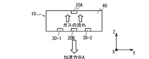
- the gas acceleration sensor 10 includes two heaters 20 (first heater 20A and second heater 20B) as components.
- first heater 20A and second heater 20B the description which overlaps with 1st Embodiment is abbreviate
- omitted suitably.
- the first heater 20A is formed on the cap chip 200 side, and is the same as the heater 20 in the first embodiment.
- the second heater 20B is formed on the base chip 100 side. More specifically, the second heater 20 ⁇ / b> B is formed on the surface 101 of the base chip 100 and is exposed to the space 40. In the X direction, the first temperature sensor 30-1 and the second temperature sensor 30-2 are arranged to face each other with the second heater 20B interposed therebetween. The first heater 20A and the second heater 20B may be provided so as to face each other.
- FIG. 16 conceptually shows a state in which “acceleration in the ⁇ Z direction” is applied to the semiconductor device.
- the gas in the space 40 cannot follow the movement of the semiconductor device. Therefore, in the space 40, a gas flow (relative movement) occurs in a direction (+ Z direction) opposite to the acceleration direction A ( ⁇ Z direction).
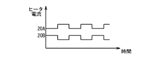
- the first heater 20A and the second heater 20B are alternately energized (ON). That is, when the first heater 20A is ON, the second heater 20B is OFF, and when the first heater 20A is OFF, the second heater 20B is ON.
- the first heater 20A is ON, the first heater 20A is located away from the temperature sensor 30, so that the temperature change detected by the temperature sensor 30 when the acceleration in the Z direction is applied is large.
- the second heater 20B is ON, since the second heater 20B is directly beside the temperature sensor 30, the temperature change detected by the temperature sensor 30 when the acceleration in the Z direction is applied is small.
- the temperature change pattern can be detected more clearly by taking the difference between the measured temperatures in both cases.
- the sensitivity and accuracy of the gas type acceleration sensor 10 are improved by a method based on the difference instead of the absolute value. For example, even if the offset value fluctuates due to changes in the surrounding environment, accurate acceleration detection is possible with this method based on the difference.
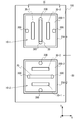
- a plurality of gas acceleration sensors 10 are provided in a semiconductor device.
- a first gas-type acceleration sensor 10-1 and a second gas-type acceleration sensor 10-2 are provided.
- the description which overlaps with 1st Embodiment is abbreviate
- two cap chips 200 are mounted on a single base chip 100.
- the periphery of the first cap chip 200-1 is surrounded by the side fill 250-1
- the periphery of the second cap chip 200-2 is surrounded by the side fill 250-2.
- the first cap chip 200-1 and the second cap chip 200-2 correspond to the first gas type acceleration sensor 10-1 and the second gas type acceleration sensor 10-2, respectively.
- the heater 20 of the first gas type acceleration sensor 10-1 is formed on the first cap chip 200-1.
- the heater 20 of the second gas type acceleration sensor 10-2 is formed in the second cap chip 200-2.
- the temperature sensor 30 of the first gas type acceleration sensor 10-1 and the temperature sensor 30 of the second gas type acceleration sensor 10-2 are formed in a single base chip 100.
- the operations of the first gas type acceleration sensor 10-1 and the second gas type acceleration sensor 10-2 are the same as those in the first embodiment.
- each of the first gas type acceleration sensor 10-1 and the second gas type acceleration sensor 10-2 is arranged so as to be able to detect acceleration in the X direction and the Z direction. Has been.
- correction processing can be performed.
- the direction in which acceleration can be detected may be different between the first gas type acceleration sensor 10-1 and the second gas type acceleration sensor 10-2.
- the in-plane direction in which acceleration can be detected is different (crossed) between the first gas acceleration sensor 10-1 and the second gas acceleration sensor 10-2.
- the first gas acceleration sensor 10-1 is arranged so as to be able to detect accelerations in two directions, the X direction and the Z direction.
- the second gas type acceleration sensor 10-2 is arranged so as to be able to detect acceleration in two directions of the Y direction and the Z direction. As a result, acceleration in all directions can be detected.
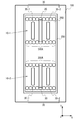
- a plurality of gas-type acceleration sensors 10 are provided in a semiconductor device, as in the fifth embodiment. However, unlike the fifth embodiment, a plurality of gas-type acceleration sensors 10 are formed using a single base chip 100 and a single cap chip 200. In addition, the description which overlaps with 5th Embodiment is abbreviate
- a single cap chip 200 is mounted on a single base chip 100.
- the periphery of the cap chip 200 is surrounded by a side fill 250.
- the heater 20 of the first gas type acceleration sensor 10-1 and the heater 20 of the second gas type acceleration sensor 10-2 are formed in a single cap chip 200.
- the temperature sensor 30 of the first gas type acceleration sensor 10-1 and the temperature sensor 30 of the second gas type acceleration sensor 10-2 are formed in a single base chip 100.
- the first gas type acceleration sensor 10-1 and the second gas type acceleration sensor are interposed between the first gas type acceleration sensor 10-1 and the second gas type acceleration sensor 10-2.
- a “partition” for isolating the sensor 10-2 is formed.
- An insulating film may be formed as the partition.
- the partition may be formed by using the bump 300.
- a “bump row 300A” is formed by a plurality of bumps 300 arranged in a row without a gap.
- the bump row 300A may be used as a partition. Since the bump example 300A is conductive, care must be taken so that the bump row 300A does not contact the temperature sensor 30 on the base chip 100 side. Further, the bump rows 300A may be arranged so as to have a slight gap as long as they do not affect the adjacent gas type acceleration sensor.
- each of the first gas type acceleration sensor 10-1 and the second gas type acceleration sensor 10-2 is arranged so as to be able to detect acceleration in two directions of the X direction and the Z direction. Has been.
- correction processing can be performed.
- the direction in which acceleration can be detected may be different between the first gas type acceleration sensor 10-1 and the second gas type acceleration sensor 10-2.
- the in-plane direction in which acceleration can be detected is different (crossed) between the first gas type acceleration sensor 10-1 and the second gas type acceleration sensor 10-2.
- the first gas acceleration sensor 10-1 is arranged so as to be able to detect accelerations in two directions, the X direction and the Z direction.
- the second gas type acceleration sensor 10-2 is arranged so as to be able to detect acceleration in two directions of the Y direction and the Z direction. As a result, acceleration in all directions can be detected.
Landscapes
- Physics & Mathematics (AREA)
- General Physics & Mathematics (AREA)
- Pressure Sensors (AREA)
Abstract
Description
1-1.基本構成
図1は、第1の実施の形態に係る半導体装置の構成を概念的に示す平面図である。図2Aは、図1中の線A-A’に沿った断面構造を概念的に示している。図2Bは、図1中の線B-B’に沿った断面構造を概念的に示している。
図3は、半導体装置に加速がかかっていない状態(例:静止状態)での温度分布を示している。縦軸が温度を表し、横軸がX方向における位置を表している。この状態では、ヒータ20の位置を中心とした対称的な温度分布が形成される。
図6は、本実施の形態に係る半導体装置の構造の一例を示している。
図9A~図9Lは、本実施の形態に係る半導体装置の製造方法の一例を示す断面図である。
上記の第1の実施の形態では、ヒータ20が上側のキャップチップ200に形成され、温度センサ30が下側のベースチップ100に形成されていた。この関係は逆であってもよい。すなわち、ヒータ20が下側のベースチップ100に形成され、温度センサ30が上側のキャップチップ200に形成されてもよい。第2の実施の形態では、この場合を説明する。尚、第1の実施の形態と重複する説明は適宜省略する。
図13は、第3の実施の形態に係る半導体装置の構成を概念的に示している。第1の実施の形態(図2A参照)と比較して、ガス式加速度センサ10は、更に、第3温度センサ30-3及び第4温度センサ30-4を構成要素として備えている。尚、第1の実施の形態と重複する説明は適宜省略する。
図15は、第4の実施の形態に係る半導体装置の構成を概念的に示している。第1の実施の形態(図2A参照)と比較して、ガス式加速度センサ10は、2つのヒータ20(第1ヒータ20Aと第2ヒータ20B)を構成要素として備えている。尚、第1の実施の形態と重複する説明は適宜省略する。
第5の実施の形態では、半導体装置に、複数のガス式加速度センサ10が設けられる。ここでは、例として、2個のガス式加速度センサ10(第1ガス式加速度センサ10-1と第2ガス式加速度センサ10-2)が設けられている場合を考える。尚、第1の実施の形態と重複する説明は適宜省略する。
第6の実施の形態では、上記の第5の実施の形態と同様に、半導体装置に、複数のガス式加速度センサ10が設けられる。但し、第5の実施の形態とは異なり、単一のベースチップ100と単一のキャップチップ200を用いて複数のガス式加速度センサ10が形成される。尚、第5の実施の形態と重複する説明は適宜省略する。
Claims (18)
- ヒータ、第1温度センサ及び第2温度センサを構成要素として含むガス式加速度センサと、
前記構成要素のうち前記ヒータが第1表面に形成された第1チップと、
前記構成要素のうち前記第1温度センサと前記第2温度センサが第2表面に形成された第2チップと、
前記第1チップと前記第2チップとを電気的に接続する接続部材と
を備え、
前記第1チップと前記第2チップは、前記第1表面と前記第2表面が対向するように、前記接続部材を介して積層されており、
前記第1チップと前記第2チップの積層方向において、前記ヒータの位置は、前記第1温度センサ及び前記第2温度センサの位置と異なっており、
前記積層方向に直交する第1面内方向において、前記第1温度センサと前記第2温度センサは、前記ヒータを挟んで対向するように配置されており、
前記第1チップと前記第2チップのうち一方が、ベースチップであり、
前記第1チップと前記第2チップのうち他方が、前記ベースチップ上に積層されたキャップチップであり、
前記キャップチップに形成された前記ガス式加速度センサの前記構成要素は、前記接続部材と直接接触している
半導体装置。 - 請求項1に記載の半導体装置であって、
前記第1チップが前記キャップチップであり、
前記第2チップが前記ベースチップである
半導体装置。 - 請求項1に記載の半導体装置であって、
前記キャップチップの半導体基板の欠陥密度は、前記ベースチップの半導体基板の欠陥密度よりも高い
半導体装置。 - 請求項3に記載の半導体装置であって、
前記ベースチップはトランジスタを有し、
前記キャップチップはトランジスタを有さない
半導体装置。 - 請求項1に記載の半導体装置であって、
前記接続部材はバンプである
半導体装置。 - 請求項1に記載の半導体装置であって、
前記積層方向と直交し且つ前記第1面内方向と交差する方向は、第2面内方向であり、
前記ガス式加速度センサの前記構成要素は、前記第2面内方向に延在するように形成された金属配線である
半導体装置。 - 請求項6に記載の半導体装置であって、
前記接続部材は、前記第2面内方向において離間して設けられた一対の接続部材を含み、
前記キャップチップに形成された前記ガス式加速度センサの前記構成要素の各々は、前記一対の接続部材と直接接触している
半導体装置。 - 請求項1に記載の半導体装置であって、
前記ガス式加速度センサは、更に、第3温度センサと第4温度センサを前記構成要素として含み、
前記第3温度センサ及び前記第4温度センサは、前記第1チップの前記第1表面に形成されており、
前記第1面内方向において、前記第3温度センサと前記第4温度センサは、前記ヒータを挟んで対向するように配置されている
半導体装置。 - 請求項1に記載の半導体装置であって、
前記ガス式加速度センサは、更に、他のヒータを前記構成要素として含み、
前記他のヒータは、前記第2チップの前記第2表面に形成されており、
前記第1面内方向において、前記第1温度センサと前記第2温度センサは、前記他のヒータを挟んで対向するように配置されている
半導体装置。 - 請求項9に記載の半導体装置であって、
前記ヒータと前記他のヒータは交互に通電される
半導体装置。 - 請求項1に記載の半導体装置であって、
前記ガス式加速度センサの数は複数であり、
前記複数のガス式加速度センサの各々が、前記構成要素を含んでいる
半導体装置。 - 請求項11に記載の半導体装置であって、
前記複数のガス式加速度センサは、第1ガス式加速度センサと第2ガス式加速度センサとを含み、
前記第1ガス式加速度センサに関する前記第1面内方向は、前記第2ガス式加速度センサに関する前記第1面内方方向と交差している
半導体装置。 - 請求項11に記載の半導体装置であって、
前記キャップチップの数は複数であり、
前記複数のキャップチップのそれぞれが前記複数のガス式加速度センサに対応している
半導体装置。 - 請求項11に記載の半導体装置であって、
前記複数のガス式加速度センサ間には、前記複数のガス式加速度センサのそれぞれを隔離するパーティションが形成されている
半導体装置。 - 請求項14に記載の半導体装置であって、
前記パーティションは、複数のバンプで形成されている
半導体装置。 - 請求項1に記載の半導体装置であって、
前記ベースチップ上と前記キャップチップ上には絶縁層が形成されており、前記ベースチップ上の絶縁層の層数は前記キャップチップ上の絶縁層の層数より多い
半導体装置。 - 加速度センサを構成する温度センサが配置された第1チップと、
前記加速度センサを構成するヒータが配置された第2チップと、
前記第1チップと前記第2チップとの間に配置され、前記温度センサと前記ヒータが配置される空間を区画する接続部材とを有し、
前記ヒータの両端は前記接続部材と直接接触して前記第1チップと電気的に接続される
半導体装置。 - 半導体装置の製造方法であって、
前記半導体装置は、ヒータ、第1温度センサ及び第2温度センサを構成要素として含むガス式加速度センサを備え、
前記製造方法は、
第1チップの第1表面上に、前記構成要素のうち前記ヒータを形成する工程と、
第2チップの第2表面上に、前記構成要素のうち前記第1温度センサと前記第2温度センサを形成する工程と、
前記第1チップと前記第2チップを、前記第1表面と前記第2表面が対向するように、接続部材を介してフリップ接続する工程と
を含み、
前記第1チップと前記第2チップの積層方向において、前記ヒータの位置は、前記第1温度センサ及び前記第2温度センサの位置と異なっており、
前記積層方向に直交する第1面内方向において、前記第1温度センサと前記第2温度センサは、前記ヒータを挟んで対向するように配置され、
前記第1チップと前記第2チップのうち一方が、ベースチップであり、
前記第1チップと前記第2チップのうち他方が、前記ベースチップ上に積層されたキャップチップであり、
前記キャップチップに形成された前記ガス式加速度センサの前記構成要素は、前記接続部材と直接接触する
半導体装置の製造方法。
Priority Applications (3)
| Application Number | Priority Date | Filing Date | Title |
|---|---|---|---|
| PCT/JP2012/073382 WO2014041648A1 (ja) | 2012-09-12 | 2012-09-12 | 半導体装置 |
| JP2014535294A JP5902305B2 (ja) | 2012-09-12 | 2012-09-12 | 半導体装置 |
| US14/427,438 US9322837B2 (en) | 2012-09-12 | 2012-09-12 | Semiconductor device |
Applications Claiming Priority (1)
| Application Number | Priority Date | Filing Date | Title |
|---|---|---|---|
| PCT/JP2012/073382 WO2014041648A1 (ja) | 2012-09-12 | 2012-09-12 | 半導体装置 |
Publications (1)
| Publication Number | Publication Date |
|---|---|
| WO2014041648A1 true WO2014041648A1 (ja) | 2014-03-20 |
Family
ID=50277802
Family Applications (1)
| Application Number | Title | Priority Date | Filing Date |
|---|---|---|---|
| PCT/JP2012/073382 Ceased WO2014041648A1 (ja) | 2012-09-12 | 2012-09-12 | 半導体装置 |
Country Status (3)
| Country | Link |
|---|---|
| US (1) | US9322837B2 (ja) |
| JP (1) | JP5902305B2 (ja) |
| WO (1) | WO2014041648A1 (ja) |
Families Citing this family (3)
| Publication number | Priority date | Publication date | Assignee | Title |
|---|---|---|---|---|
| US9490003B2 (en) * | 2011-03-31 | 2016-11-08 | Intel Corporation | Induced thermal gradients |
| US9658678B2 (en) | 2011-03-31 | 2017-05-23 | Intel Corporation | Induced thermal gradients |
| CN113325199B (zh) * | 2021-06-09 | 2022-04-29 | 东南大学 | 一种热电堆式高灵敏度柔性加速度传感器及其制备方法 |
Citations (7)
| Publication number | Priority date | Publication date | Assignee | Title |
|---|---|---|---|---|
| JPH07260820A (ja) * | 1994-03-24 | 1995-10-13 | Honda Motor Co Ltd | 多軸加速度センサ |
| JPH08330476A (ja) * | 1995-05-31 | 1996-12-13 | Toshiba Corp | 樹脂封止型半導体装置 |
| JPH10332455A (ja) * | 1997-06-02 | 1998-12-18 | Ricoh Co Ltd | フローセンサ及びその製造方法 |
| JP2001227902A (ja) * | 2000-02-16 | 2001-08-24 | Mitsubishi Electric Corp | 半導体装置 |
| JP2004037105A (ja) * | 2002-06-28 | 2004-02-05 | Akashi Corp | 物理量検出器及び物理量検出器の製造方法 |
| JP2005351892A (ja) * | 2004-06-09 | 2005-12-22 | Memsic Inc | Z軸熱加速度計 |
| JP2008039519A (ja) * | 2006-08-03 | 2008-02-21 | Rohm Co Ltd | 加速度センサ |
Family Cites Families (12)
| Publication number | Priority date | Publication date | Assignee | Title |
|---|---|---|---|---|
| DE69510569T2 (de) | 1994-01-20 | 1999-10-28 | Honda Giken Kogyo K.K., Tokio/Tokyo | Beschleunigungsmessaufnehmer |
| JP3259645B2 (ja) | 1995-11-30 | 2002-02-25 | 松下電工株式会社 | 加速度センサ及びその製造方法 |
| US6182509B1 (en) | 1996-06-26 | 2001-02-06 | Simon Fraser University | Accelerometer without proof mass |
| JP3009104B2 (ja) | 1998-01-30 | 2000-02-14 | 富士電機株式会社 | 半導体センサおよび半導体センサ用パッケージ |
| JP2000046859A (ja) | 1998-07-28 | 2000-02-18 | Omron Corp | 加速度センサ |
| US7021821B2 (en) | 2004-05-28 | 2006-04-04 | Honeywell International Inc. | Differential thermal sensors |
| JP4975972B2 (ja) * | 2005-03-15 | 2012-07-11 | 日立オートモティブシステムズ株式会社 | 物理量センサ |
| JP4495711B2 (ja) * | 2006-10-27 | 2010-07-07 | 株式会社日立製作所 | 機能素子及びその製造方法 |
| JP2009122041A (ja) | 2007-11-16 | 2009-06-04 | Ricoh Co Ltd | 複合センサー |
| JP2012189571A (ja) * | 2011-02-24 | 2012-10-04 | Renesas Electronics Corp | 半導体装置及びその製造方法 |
| DE102012200121A1 (de) * | 2012-01-05 | 2013-07-11 | Robert Bosch Gmbh | Vorrichtung zur Erfassung mindestens einer Strömungseigenschaft eines fluiden Mediums |
| US8969978B2 (en) * | 2012-04-27 | 2015-03-03 | Melexis Technologies Nv | TMAP sensor systems and methods for manufacturing those |
-
2012
- 2012-09-12 WO PCT/JP2012/073382 patent/WO2014041648A1/ja not_active Ceased
- 2012-09-12 US US14/427,438 patent/US9322837B2/en not_active Expired - Fee Related
- 2012-09-12 JP JP2014535294A patent/JP5902305B2/ja not_active Expired - Fee Related
Patent Citations (7)
| Publication number | Priority date | Publication date | Assignee | Title |
|---|---|---|---|---|
| JPH07260820A (ja) * | 1994-03-24 | 1995-10-13 | Honda Motor Co Ltd | 多軸加速度センサ |
| JPH08330476A (ja) * | 1995-05-31 | 1996-12-13 | Toshiba Corp | 樹脂封止型半導体装置 |
| JPH10332455A (ja) * | 1997-06-02 | 1998-12-18 | Ricoh Co Ltd | フローセンサ及びその製造方法 |
| JP2001227902A (ja) * | 2000-02-16 | 2001-08-24 | Mitsubishi Electric Corp | 半導体装置 |
| JP2004037105A (ja) * | 2002-06-28 | 2004-02-05 | Akashi Corp | 物理量検出器及び物理量検出器の製造方法 |
| JP2005351892A (ja) * | 2004-06-09 | 2005-12-22 | Memsic Inc | Z軸熱加速度計 |
| JP2008039519A (ja) * | 2006-08-03 | 2008-02-21 | Rohm Co Ltd | 加速度センサ |
Also Published As
| Publication number | Publication date |
|---|---|
| US20150233964A1 (en) | 2015-08-20 |
| JP5902305B2 (ja) | 2016-04-13 |
| US9322837B2 (en) | 2016-04-26 |
| JPWO2014041648A1 (ja) | 2016-08-12 |
Similar Documents
| Publication | Publication Date | Title |
|---|---|---|
| KR100780496B1 (ko) | 반도체 장치, 자기 센서 및 자기 센서 유닛 | |
| US7762134B2 (en) | Dynamic quantity sensor | |
| JP3516608B2 (ja) | 半導体装置 | |
| JP2006119042A (ja) | 加速度センサチップパッケージ及びその製造方法 | |
| JP5902305B2 (ja) | 半導体装置 | |
| JP2005180930A (ja) | 半導体センサ装置及びその製造方法 | |
| JP2008101980A (ja) | 容量式半導体センサ装置 | |
| KR20150141418A (ko) | 금속의 허메틱 실을 갖는 관성센서모듈 및 그를 사용한 다축센서 | |
| TWI518886B (zh) | 光感裝置及其製法 | |
| JP2007132687A (ja) | センサ用パッケージおよびこれを用いた検出装置 | |
| JP5912701B2 (ja) | 磁気検出装置の製造方法 | |
| JP2010164411A (ja) | 薄膜型ガスセンサ | |
| JP6464770B2 (ja) | 物理量センサおよびその製造方法 | |
| CN1944236B (zh) | 半导体器件和其制造方法以及检查方法 | |
| JP2008008672A (ja) | 加速度センサ | |
| JP2010008172A (ja) | 半導体装置 | |
| JP2008209163A (ja) | センサ装置 | |
| JP2007263766A (ja) | センサ装置 | |
| JP3938202B1 (ja) | センサパッケージの製造方法 | |
| US20250155466A1 (en) | Method For Manufacturing Electronic Device | |
| JP2008122304A (ja) | 静電容量式加速度センサ | |
| JP4175343B2 (ja) | 半導体ペレット及び半導体装置 | |
| JP4000168B2 (ja) | センサ装置 | |
| JP5069410B2 (ja) | センサエレメント | |
| JP6585449B2 (ja) | 角速度センサ |
Legal Events
| Date | Code | Title | Description |
|---|---|---|---|
| 121 | Ep: the epo has been informed by wipo that ep was designated in this application |
Ref document number: 12884422 Country of ref document: EP Kind code of ref document: A1 |
|
| ENP | Entry into the national phase |
Ref document number: 2014535294 Country of ref document: JP Kind code of ref document: A |
|
| WWE | Wipo information: entry into national phase |
Ref document number: 14427438 Country of ref document: US |
|
| NENP | Non-entry into the national phase |
Ref country code: DE |
|
| 122 | Ep: pct application non-entry in european phase |
Ref document number: 12884422 Country of ref document: EP Kind code of ref document: A1 |