WO2014038450A1 - メモリ制御装置、携帯端末、メモリ制御プログラムおよびコンピュータ読み取り可能な記録媒体 - Google Patents
メモリ制御装置、携帯端末、メモリ制御プログラムおよびコンピュータ読み取り可能な記録媒体 Download PDFInfo
- Publication number
- WO2014038450A1 WO2014038450A1 PCT/JP2013/073017 JP2013073017W WO2014038450A1 WO 2014038450 A1 WO2014038450 A1 WO 2014038450A1 JP 2013073017 W JP2013073017 W JP 2013073017W WO 2014038450 A1 WO2014038450 A1 WO 2014038450A1
- Authority
- WO
- WIPO (PCT)
- Prior art keywords
- read
- time
- period
- memory control
- write
- Prior art date
- Legal status (The legal status is an assumption and is not a legal conclusion. Google has not performed a legal analysis and makes no representation as to the accuracy of the status listed.)
- Ceased
Links
Images




Classifications
-
- G—PHYSICS
- G06—COMPUTING OR CALCULATING; COUNTING
- G06T—IMAGE DATA PROCESSING OR GENERATION, IN GENERAL
- G06T1/00—General purpose image data processing
- G06T1/60—Memory management
-
- G—PHYSICS
- G09—EDUCATION; CRYPTOGRAPHY; DISPLAY; ADVERTISING; SEALS
- G09G—ARRANGEMENTS OR CIRCUITS FOR CONTROL OF INDICATING DEVICES USING STATIC MEANS TO PRESENT VARIABLE INFORMATION
- G09G3/00—Control arrangements or circuits, of interest only in connection with visual indicators other than cathode-ray tubes
- G09G3/20—Control arrangements or circuits, of interest only in connection with visual indicators other than cathode-ray tubes for presentation of an assembly of a number of characters, e.g. a page, by composing the assembly by combination of individual elements arranged in a matrix no fixed position being assigned to or needed to be assigned to the individual characters or partial characters
-
- G—PHYSICS
- G09—EDUCATION; CRYPTOGRAPHY; DISPLAY; ADVERTISING; SEALS
- G09G—ARRANGEMENTS OR CIRCUITS FOR CONTROL OF INDICATING DEVICES USING STATIC MEANS TO PRESENT VARIABLE INFORMATION
- G09G3/00—Control arrangements or circuits, of interest only in connection with visual indicators other than cathode-ray tubes
- G09G3/20—Control arrangements or circuits, of interest only in connection with visual indicators other than cathode-ray tubes for presentation of an assembly of a number of characters, e.g. a page, by composing the assembly by combination of individual elements arranged in a matrix no fixed position being assigned to or needed to be assigned to the individual characters or partial characters
- G09G3/34—Control arrangements or circuits, of interest only in connection with visual indicators other than cathode-ray tubes for presentation of an assembly of a number of characters, e.g. a page, by composing the assembly by combination of individual elements arranged in a matrix no fixed position being assigned to or needed to be assigned to the individual characters or partial characters by control of light from an independent source
- G09G3/36—Control arrangements or circuits, of interest only in connection with visual indicators other than cathode-ray tubes for presentation of an assembly of a number of characters, e.g. a page, by composing the assembly by combination of individual elements arranged in a matrix no fixed position being assigned to or needed to be assigned to the individual characters or partial characters by control of light from an independent source using liquid crystals
-
- G—PHYSICS
- G09—EDUCATION; CRYPTOGRAPHY; DISPLAY; ADVERTISING; SEALS
- G09G—ARRANGEMENTS OR CIRCUITS FOR CONTROL OF INDICATING DEVICES USING STATIC MEANS TO PRESENT VARIABLE INFORMATION
- G09G3/00—Control arrangements or circuits, of interest only in connection with visual indicators other than cathode-ray tubes
- G09G3/20—Control arrangements or circuits, of interest only in connection with visual indicators other than cathode-ray tubes for presentation of an assembly of a number of characters, e.g. a page, by composing the assembly by combination of individual elements arranged in a matrix no fixed position being assigned to or needed to be assigned to the individual characters or partial characters
- G09G3/34—Control arrangements or circuits, of interest only in connection with visual indicators other than cathode-ray tubes for presentation of an assembly of a number of characters, e.g. a page, by composing the assembly by combination of individual elements arranged in a matrix no fixed position being assigned to or needed to be assigned to the individual characters or partial characters by control of light from an independent source
- G09G3/36—Control arrangements or circuits, of interest only in connection with visual indicators other than cathode-ray tubes for presentation of an assembly of a number of characters, e.g. a page, by composing the assembly by combination of individual elements arranged in a matrix no fixed position being assigned to or needed to be assigned to the individual characters or partial characters by control of light from an independent source using liquid crystals
- G09G3/3611—Control of matrices with row and column drivers
-
- G—PHYSICS
- G09—EDUCATION; CRYPTOGRAPHY; DISPLAY; ADVERTISING; SEALS
- G09G—ARRANGEMENTS OR CIRCUITS FOR CONTROL OF INDICATING DEVICES USING STATIC MEANS TO PRESENT VARIABLE INFORMATION
- G09G5/00—Control arrangements or circuits for visual indicators common to cathode-ray tube indicators and other visual indicators
- G09G5/36—Control arrangements or circuits for visual indicators common to cathode-ray tube indicators and other visual indicators characterised by the display of a graphic pattern, e.g. using an all-points-addressable [APA] memory
- G09G5/39—Control of the bit-mapped memory
- G09G5/393—Arrangements for updating the contents of the bit-mapped memory
-
- G—PHYSICS
- G09—EDUCATION; CRYPTOGRAPHY; DISPLAY; ADVERTISING; SEALS
- G09G—ARRANGEMENTS OR CIRCUITS FOR CONTROL OF INDICATING DEVICES USING STATIC MEANS TO PRESENT VARIABLE INFORMATION
- G09G2320/00—Control of display operating conditions
- G09G2320/02—Improving the quality of display appearance
- G09G2320/0247—Flicker reduction other than flicker reduction circuits used for single beam cathode-ray tubes
-
- G—PHYSICS
- G09—EDUCATION; CRYPTOGRAPHY; DISPLAY; ADVERTISING; SEALS
- G09G—ARRANGEMENTS OR CIRCUITS FOR CONTROL OF INDICATING DEVICES USING STATIC MEANS TO PRESENT VARIABLE INFORMATION
- G09G2340/00—Aspects of display data processing
- G09G2340/14—Solving problems related to the presentation of information to be displayed
-
- G—PHYSICS
- G09—EDUCATION; CRYPTOGRAPHY; DISPLAY; ADVERTISING; SEALS
- G09G—ARRANGEMENTS OR CIRCUITS FOR CONTROL OF INDICATING DEVICES USING STATIC MEANS TO PRESENT VARIABLE INFORMATION
- G09G2350/00—Solving problems of bandwidth in display systems
-
- G—PHYSICS
- G09—EDUCATION; CRYPTOGRAPHY; DISPLAY; ADVERTISING; SEALS
- G09G—ARRANGEMENTS OR CIRCUITS FOR CONTROL OF INDICATING DEVICES USING STATIC MEANS TO PRESENT VARIABLE INFORMATION
- G09G2360/00—Aspects of the architecture of display systems
- G09G2360/12—Frame memory handling
-
- G—PHYSICS
- G09—EDUCATION; CRYPTOGRAPHY; DISPLAY; ADVERTISING; SEALS
- G09G—ARRANGEMENTS OR CIRCUITS FOR CONTROL OF INDICATING DEVICES USING STATIC MEANS TO PRESENT VARIABLE INFORMATION
- G09G2360/00—Aspects of the architecture of display systems
- G09G2360/12—Frame memory handling
- G09G2360/125—Frame memory handling using unified memory architecture [UMA]
-
- G—PHYSICS
- G09—EDUCATION; CRYPTOGRAPHY; DISPLAY; ADVERTISING; SEALS
- G09G—ARRANGEMENTS OR CIRCUITS FOR CONTROL OF INDICATING DEVICES USING STATIC MEANS TO PRESENT VARIABLE INFORMATION
- G09G2360/00—Aspects of the architecture of display systems
- G09G2360/18—Use of a frame buffer in a display terminal, inclusive of the display panel
Definitions
- the present invention relates to a memory control device that writes data transferred from a host processor to a frame memory, reads the data written in the frame memory, and transfers the data to a display panel such as an LCD (Liquid Crystal Display).
- the present invention relates to a portable terminal provided with a memory control device, a memory control program, and a computer-readable recording medium on which the memory control program is recorded.
- a host processor hereinafter simply referred to as “host”
- a display panel such as an LCD
- the image data is transferred to a frame memory (hereinafter simply referred to as “memory”) in an LCDC (LCD Controller). After being temporarily saved, it is output to the display panel. This eliminates the need to transfer image data from the host when the display data is not updated.
- LCDC LCD Controller
- the frame rate conversion apparatus includes a memory control unit that inputs / outputs data to / from a common memory, an overtaking prediction unit that predicts a frame in which overtaking of input / output of data to / from the memory occurs, and an overtaking prediction unit, And a memory write control unit that stops writing to the memory when overtaking is predicted to occur.
- Patent Document 2 discloses a method for updating a buffer.
- This method is a method for conveying timing information over a communication link between a first processor and a second processor. Also, in this method, the communication link is in a dormant mode and schedules time events in the first processor to convey timing information to the second processor. Further, in this method, when a time event occurs, link wakeup by the first processor is started, link wakeup is detected in the second processor, and the detected link wakeup timing is used for the timing information conveyed. The first processor and the second processor are synchronized.
- Patent Document 3 discloses a memory access control device.
- the write processing circuit determines that the writable area of the memory is equal to or smaller than the data size to be written to the memory, the data write processing is stopped.
- Japanese Patent Publication Japanese Patent Laid-Open No. 2005-124167 (published on May 12, 2005)” Japanese Patent Publication “JP 2011-41290 (published on Feb. 24, 2011)” Japanese Patent Publication “Japanese Patent Laid-Open No. 2007-304832 (published on November 22, 2007)”
- Patent Documents 1 to 3 have the following problems.
- the host waits until a safe timing, and in the worst case, a waiting time of one frame at maximum may occur. There is.
- a negative effect since the host side frame buffer cannot be released until the data transfer for updating the image data is completed, even if the host side has a double buffer structure, until the next image data starts to be created, There was a problem that a waiting time was required and this would cause frame dropping. Further, even when there is no update of the next image data, the host side operation cannot be stopped until the transfer is completed, and thus there is a problem that power is consumed wastefully for a certain period of time.
- the present invention has been made in view of the above-described conventional problems, such as a memory control device that can avoid frame dropping, reduce unnecessary power consumption, and can be made inconspicuous even if tearing occurs.
- the purpose is to provide.
- a memory control device reads a data write operation to write data transferred from a host to a frame memory, and reads the data written to the frame memory.
- a memory control device that executes a read operation transferred to a display control unit, a read period that is a period from the start to the end of the read operation, and a write period that is a period from the start to the end of the write operation ,
- the reading operation is temporarily stopped at the time point specified by the overtaking time point specifying means for specifying the time point immediately before and the overtaking time point specifying means, and the reading operation in the frame memory is performed at a predetermined reading restart time point.
- Read reset control means for performing a process of redoing the data read operation from the start position.
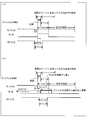
- 5 is a timing chart showing an example of the operation of the memory control device, where (a) shows an example of the operation when the start time of the write operation in the case of Tin> Tout is not in the danger period, and (b) An example of the operation when the start time of the write operation is in the danger period is shown.
- FIG. 6 is a timing chart showing an example of the operation of the memory control device, where (a) shows an example of the operation when the start time of the write operation in the case of Tin ⁇ Tout is not in the danger period, and (b) An example of the operation when the start time of the write operation is in the danger period is shown. It is a timing chart which shows the example of the processing method when tearing generate
- FIGS. 1 to 7 An embodiment of the present invention will be described with reference to FIGS. 1 to 7 as follows. Descriptions of configurations other than those described in the following specific items may be omitted as necessary. However, in the case where they are described in other items, the configurations are the same. For convenience of explanation, members having the same functions as those shown in each item are given the same reference numerals, and the explanation thereof is omitted as appropriate.
- FIG. 1 is a block diagram showing the configuration of the image transfer system 1.
- the image transfer system 1 includes a host processor (host, memory control device) 2, an LCD controller (memory control device) 3, and an LCD (display control unit) 4.
- the image transfer system 1 according to the present embodiment has a write operation for writing image data (data) transferred from the host processor 2 to a frame memory 31 described later, and reads the image data written in the frame memory 31 to the LCD 4. It is a device that performs a read operation to transfer.
- the form in which the LCD 4 is excluded from the image transfer system 1 corresponds to an embodiment of the memory control device of the present invention.
- the host processor 2 is a host processor (CPU: Central Processing Unit) of the apparatus main body (for example, the portable terminal 10 shown in FIG. 2), and controls the apparatus main body (transfer) and transfers it to the LCD 4.
- Image data various signals such as REQ (Request) signal, various control commands such as handshake flag and BTA (Bus Turnaround), VSS (Vertical Sync Start) packet and BS (Blanking Start)
- REQ Request
- BTA Bus Turnaround
- VSS Very Sync Start
- BS Binary Sync Start
- the LCD controller 3 performs various operations such as an image data input / output mechanism, an operation for writing image data transferred from the host processor 2 to the frame memory 31, and a read operation for reading image data from the frame memory 31 and transferring it to the LCD 4. The processing is performed.
- the LCD controller 3 includes at least a frame memory 31, a read reset control unit (read reset control means) 32, a determination unit (passing time specifying means) 34, and a control register 35.
- the frame memory 31 is an image memory that can store at least one frame of image data transferred from the host processor 2.
- the read reset control unit 32 uses a determination unit 34 described later to read the current read position in the frame memory 31 when the operation speed of the read operation> the operation speed of the write operation (hereinafter referred to as Tin> Tout). It is determined that the pointer (hereinafter simply described as “rp”) catches up with or immediately before the write pointer (hereinafter simply described as “wp”) indicating the current writing position in the frame memory 31 ( The read operation is temporarily stopped at the specified time (the time when rp catches up to wp or immediately before), and the read operation in the frame memory 31 is started at the predetermined read restart time. The image data reading operation is performed again from the position.
- the read reset control unit 32 determines the time at which wp catches up to rp or immediately before by the determination unit 34 described later. When it is determined that it is the time, the reading operation is temporarily stopped at the specified time, and the image data reading operation is restarted from the position where the reading operation in the frame memory 31 is started at that time (reading restart time). It is like that. More specifically, the read reset control unit 32 temporarily stops the read operation and restarts the read operation from the beginning of the frame. A driving voltage is injected into the liquid crystal panel (not shown) of the LCD 4 up to an intermediate line, but the same driving voltage is injected again from the first line and driven to the end of the frame to drive the driving voltage for one frame. Control overwriting.
- the “read resume time” may be a time delayed by at least the difference between the write period and the read period from the start of the read operation (Outdly). It may be a time point (delay time after reset) that goes back by the reading period from the end point of the operation.
- the “reading restart time” is preferably the time when the reading operation is temporarily stopped.
- the determination unit 34 determines whether or not the start time of the write operation exists in the dangerous period when the lengths of the read period Tout and the write period Tin are different, and the rp in the frame memory 31 is set to wp.
- Various determination processes are performed such as specifying (determining) the time point that catches up or immediately before it, or the time point that wp catches up to rp or the time point immediately before it.
- the determination unit 34 may be employed.
- Control register 35 stores various control commands from the host processor 2 and transmits the stored control commands to the host processor 2.
- Examples of the control command include various data used for setting parameters in each unit (circuit), for example, an image size, a line size, a frequency, a transfer waiting time, a specified value for calculating a dangerous period, and the like.
- a handshake flag or the like can be exemplified as an example of a control command that the control register 35 passes to the host processor 2.
- LCD4 The LCD 4 displays image data transferred from the host processor 2 via the LCD controller 3.
- the LCD 4 of the present embodiment is, for example, a liquid crystal panel using an oxide semiconductor (hereinafter referred to as “oxide semiconductor liquid crystal panel”.
- oxide semiconductor liquid crystal panel examples include an oxide made of indium, gallium, and zinc). Preferably there is.
- the “dangerous period” (indicated as “dangerous” in FIG. 3) is a period determined in advance based on at least the difference between the read period Tout and the write period Tin with the end point of the read operation as a reference.
- the danger period
- writing period Tin ⁇ reading period Tout.
- the “delay time” is a period determined in advance based on the difference between the read period Tout and the write period Tin.
- the “delay period” is preferably a period longer than the difference between the read period Tout and the write period Tin.
- “delay period”
- + (predetermined margin) write period Tin ⁇ read period Tout + (predetermined margin).
- the delay period
- Tin ⁇ Tout.
- FIG. 3 is a timing chart showing an example of the operation of the image transfer system 1.
- FIG. 3 (a) is transferred at the start time of the writing operation (the time point indicated by the position indicated by the downward arrow “DSI input” shown in FIG. 3) or prior to the image data writing operation described later. This is an example of the operation when the information is not within the danger period.
- (b) of FIG. 3 shows an example of the operation when the start time of the write operation is within the danger period.
- FIG. 3B shows the operation when the operation speed of the read operation> the operation speed of the write operation (Tin> Tout).
- the determination unit 34 determines that the start time of the write operation is within the danger period and specifies that rp in the frame memory 31 catches up to wp or is the time immediately before it
- read reset control The unit 32 temporarily stops the read operation at the specified time (when rp catches up to wp or immediately before), and waits for the delay period (Tin ⁇ Tout) from the time when the write operation is started.
- the image data reading operation is started again from the position where the reading operation in the frame memory 31 is started.
- the determination unit 34 it is not always necessary to interpose the step of determining whether or not the start time of the write operation exists within the danger period as in this embodiment. For example, if the time point at which rp catches up to wp or the time point just before it is specified at the time of the falling time of Hsync at all times or not is determined, it is determined whether or not the write operation start time exists within the danger period. It is not necessary to determine in advance.
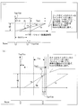
- FIG. 5 is a timing chart showing an example of a processing method (read reset control) when tearing occurs.
- FIG. 5A shows a case where Tin> Tout.
- the unit of the horizontal axis is time
- the unit of the vertical axis is the number of lines for writing or reading image data in the frame memory 31 in this embodiment.
- VW indicates the width of the vertical synchronization period (here, the total number of lines of image data recorded in the frame memory 31)
- Tvp + Tvb indicates the vertical synchronization signal pulse period and the vertical back porch period.
- the sum period here, the number of lines in the read operation).
- rp is a read pointer (a current data reading position in the frame memory 31)
- wp is a write pointer (a data writing position in the frame memory 31 at the current time).
- the graph shown in the figure shows the transition of rp and wp with time. Further, the broken line graph of rp (rp on the left side with respect to the paper surface) corresponds to the state before the execution of the read reset control, and the solid line graph of rp (rp on the right side with respect to the paper surface) indicates the read reset. Corresponds to the state after execution of control.
- the solid line graph of wp shown in the figure intersects with the broken line graph of rp at the point P1, which indicates that the tailing occurs at the point P1.
- the solid line graph of rp corresponds to the state after execution of the read reset control, and intersects at a point on a straight line (broken line) parallel to the horizontal axis that is separated from the horizontal axis by VW in the positive direction. This indicates that no tearing occurs due to the re-reading of the read operation from the beginning of.
- the “delay time after reset” indicates the time between the time point that goes back by the read period from the end point of the write operation and the time point of the point P1.
- FIG. 6 is a flowchart showing an example of read reset control on the LCD controller 3 side regarding the operation of the image transfer system 1.
- step S71 shown in the figure the LCD controller 3 waits for the occurrence of an image input start event from the host processor 2 and proceeds to S72.
- the “image input start event” is reception of information that is always transferred prior to the image data writing operation, for example.
- the information is a VSS (Vertical Sync Start) packet in a DSI (Display Serial Interface) video mode in a MIPI (Mobile Industry Processor Interface) video mode.
- VSS Very Sync Start
- DSI Display Serial Interface
- MIPI Mobile Industry Processor Interface
- the determination unit 34 determines whether the start time of the write operation (the time indicated by the downward arrow of the DSI input shown in FIGS. 3 and 4) is within the danger period. As a result, when the start time of the writing operation is within the danger period, the process proceeds to S73 (YES). On the other hand, when the start time of the write operation is not within the danger period, the process returns to S71 (NO).
- the operation of S72 described above may or may not exist.
- a flow that directly proceeds from S71 to S73 may be adopted.
- the determination unit 34 monitors the time point when Hsync falls or always rp and wp.
- the read reset control unit 32 temporarily stops the line counter that generates a line address when transferring the image data to the LCD controller 3, thereby temporarily stopping the start point of the read operation, and proceeds to S75.
- the image transfer system 1 waits for a delay time (Tin-Tout) from the start of the writing operation, and then restarts the reading operation from the beginning of the frame.
- Tin-Tout a delay time
- the read operation is temporarily stopped, and the read operation is again transferred from the top of the frame to the liquid crystal driver (not shown) of the LCD 4.
- the gate driver is reset by transferring the information (Vsync information) on the Vsync signal to the liquid crystal driver of the LCD 4 again, and the drive is restarted from the first line of the LCD 4.
- the driving voltage (pixel value of each pixel) is injected into the LCD 4 up to an intermediate line, but the same driving voltage is injected again from the top line and driven to the end of the frame, and one frame's worth of time. The drive voltage is overwritten.
- FIG. 4 is a timing chart showing an example of the operation of the image transfer system 1.
- FIG. 4 (a) is transferred at the start of the writing operation (at the time indicated by the position indicated by the downward arrow of “DSI input” shown in the figure, or prior to the above-described image data writing operation.
- This is an example of the operation when the information is not within the danger period.
- FIG. 4B shows an example of the operation when the start time of the write operation is within the danger period.
- FIG. 4B shows the operation when the operation speed of the read operation ⁇ the operation speed of the write operation (Tin ⁇ Tout).
- the determination unit 34 determines that the start time of the write operation is within the danger period and the time point at which wp in the frame memory 31 catches up with rp or the time point immediately before is specified
- the read reset control unit 32 In this case, the reading operation is temporarily stopped at the time when wp catches up with rp or immediately before it, and the image data reading operation is immediately started again from the position where the reading operation in the frame memory 31 is started.
- FIG. 5B is a timing chart showing an example of a processing method (read reset control) when tearing occurs in the case of Tin ⁇ Tout.
- the graph shown in FIG. 5B shows the transition of rp and wp with respect to time.
- the rp solid line graph (the graph on the left side of the paper, hereinafter referred to as the “left graph”) corresponds to the state before the execution of the read reset control, and the rp solid line graph (on the paper surface).
- the graph on the right side (hereinafter referred to as “right graph”) corresponds to the state after the execution of the read reset control.
- the broken line graph of wp shown in the figure intersects with the graph on the left side of rp at the point P2, which indicates that the tailing occurs at the point P2.
- the graph on the right side of rp corresponds to the state after the execution of the read reset control, and indicates that no tearing occurs due to the redo of the read operation from the beginning of the frame.
- the read reset control may be executed immediately at the time immediately before that (however, in the image transfer system 1 of the present embodiment, the actual restart of reading from the read restart instruction is delayed by Tvp + Tvb. Delay occurs).
- FIG. 7 is a flowchart showing an example of read reset control on the LCD controller 3 side in the case of Tin ⁇ Tout regarding the operation of the image transfer system 1.
- the LCD controller 3 waits for an image input start request from the host processor 2 and proceeds to S82.
- the LCD controller 3 waits for an “image input start event” from the host processor 2, and proceeds to S83.
- the “image input start event” (in the present embodiment, the above-described VSS packet) is as described above.
- the determination unit 34 determines whether the start time of the write operation (the time indicated by the downward arrow of the DSI input shown in FIGS. 3 and 4) is within the danger period. As a result, when the start time of the write operation is within the danger period, the process proceeds to S84 (YES). On the other hand, when the start time of the writing operation is not within the danger period, the process returns to S81 (NO).
- the operation of S83 described above may or may not exist.
- a flow that directly proceeds from S82 to S84 may be adopted.
- the determination unit 34 monitors the time point when Hsync falls or always rp and wp.
- the read reset control unit 32 temporarily stops the line counter that generates a line address when transferring the image data to the LCD controller 3, thereby temporarily stopping the start point of the read operation, and proceeds to S86.
- the reading operation is temporarily stopped, and the reading operation is again transferred from the top of the frame to the liquid crystal driver (not shown) of the LCD 4.
- the gate driver is reset by transferring the information (Vsync information) on the Vsync signal to the liquid crystal driver of the LCD 4 again, and the drive is restarted from the first line of the LCD 4.
- the driving voltage (pixel value of each pixel) is injected into the LCD 4 up to an intermediate line, but the same driving voltage is injected again from the top line and driven to the end of the frame, and one frame's worth of time. The drive voltage is overwritten.
- tearing can be made inconspicuous by redoing the data reading operation from the position where the reading operation in the frame memory 31 is started.
- frame dropping can be avoided, wasteful power consumption can be reduced, and even if tearing occurs, it can be made inconspicuous.
- the period of the vertical synchronization signal (Vsync) is not uniform, but when the rendering update is completed, the driving period is automatically delayed by driving several frames. This is a driving method suitable for an oxide semiconductor liquid crystal panel.
- FIG. 2 is a block diagram illustrating an overall configuration of the mobile terminal 10 including the image transfer system 1 described above.
- the mobile terminal 10 includes an SDRAM, a flash memory, a camera sensor, a camera ISP, an RF, an analog baseband, Bluetooth (registered trademark), WLAN, GPS (Global Positioning System), a DTV tuner, keys, various sensors, and the like, but the configuration other than the image transfer system 1 is not related to the essence of the present invention, so the description is omitted here.
- the mobile terminal 10 Since the mobile terminal 10 according to the present embodiment includes the image transfer system 1 described above, frame dropping is avoided, and wasteful power consumption such as power consumption during the waiting time of the host processor 2 is reduced. Even if tearing occurs, a mobile terminal that can be made inconspicuous can be realized. Other effects are the same as those described in the above item (Effects of image transfer system 1), and are therefore omitted here.
- each block of the image transfer system 1, particularly each block of the LCD controller 3 may be realized by hardware by a logic circuit formed on an integrated circuit (IC chip), or a CPU (Central Processing Unit). ) May be implemented in software.
- IC chip integrated circuit
- CPU Central Processing Unit
- the image transfer system 1 includes a CPU that executes instructions of a program that realizes each function, a ROM (Read Memory) that stores the program, a RAM (Random Access Memory) that expands the program, the program,
- a storage device (recording medium) such as a memory for storing various data is provided.
- An object of the present invention is a recording medium on which a program code (execution format program, intermediate code program, source program) of a control program of the image transfer system 1 which is software that realizes the above-described functions is recorded so as to be readable by a computer. This can also be achieved by supplying the image transfer system 1 and reading and executing the program code recorded on the recording medium by the computer (or CPU or MPU).
- Examples of the recording medium include non-transitory tangible media, such as magnetic tapes and cassette tapes, magnetic disks such as floppy (registered trademark) disks / hard disks, and CD-ROM / MO.
- Discs including optical disks such as / MD / DVD / CD-R, cards such as IC cards (including memory cards) / optical cards, and semiconductor memories such as mask ROM / EPROM / EEPROM (registered trademark) / flash ROM
- logic circuits such as PLD (Programmable logic device) and FPGA (Field Programmable Gate array) can be used.
- the image transfer system 1 may be configured to be connectable to a communication network, and the program code may be supplied via the communication network.
- the communication network is not particularly limited as long as it can transmit the program code.
- the Internet intranet, extranet, LAN, ISDN, VAN, CATV communication network, virtual private network (Virtual Private Network), telephone line network, mobile communication network, satellite communication network, etc. can be used.
- the transmission medium constituting the communication network may be any medium that can transmit the program code, and is not limited to a specific configuration or type.
- wired lines such as IEEE1394, USB, power line carrier, cable TV line, telephone line, ADSL (Asymmetric Digital Subscriber Line) line, infrared rays such as IrDA and remote control, Bluetooth (registered trademark), IEEE 802.11 wireless, HDR ( It can also be used wirelessly such as High Data Rate, NFC (Near Field Communication), DLNA (Digital Living Network Alliance) (registered trademark), a mobile phone network, a satellite line, and a terrestrial digital network.
- the present invention can also be realized in the form of a computer data signal embedded in a carrier wave in which the program code is embodied by electronic transmission.
- the memory control device includes a write operation for writing data transferred from the host to the frame memory, and a read operation for reading the data written in the frame memory and transferring the data to the display control unit.
- the memory control device that executes the above-described case, the read period, which is a period from the start to the end of the read operation, and the write period, which is a period from the start to the end of the write operation, are different from each other.
- the read pointer indicating the current read position in the frame memory catches up with or immediately before the write pointer indicating the current write position in the frame memory, or the write pointer is set to the read pointer.
- the reading operation is temporarily stopped at the time point specified by the overtaking time point specifying unit and the overtaking point time point specifying unit, and when the reading operation is started in the frame memory at a predetermined reading restart point, It is preferable to include a read reset control unit that performs a process of redoing the read operation.
- the read pointer indicating the current read position in the frame memory (Hereinafter simply referred to as “rp”) catches up with or immediately before a write pointer (hereinafter simply referred to as “wp”) indicating the current writing position in the frame memory, or wp catches up with rp.
- the read operation is temporarily stopped at the time or immediately before, and the data read operation is restarted from the position where the read operation is started in the frame memory at a predetermined read restart time.
- tearing can be made inconspicuous by redoing the data read operation (from the beginning of the data) from the position where the read operation in the frame memory is started.
- frame dropping can be avoided, wasteful power consumption can be reduced, and even if tearing occurs, it can be made inconspicuous.
- the read resume time is the start of the read operation. It may be a time point delayed from the time point by at least the difference between the writing period and the reading period.
- the read resume time is the end of the write operation. It may be a time point that goes back from the time point by the reading period.
- the read operation when the operation speed of the write operation is higher than the operation speed of the read operation, the read operation is temporarily stopped at the read restart time point. It may be at that time.
- the reset control means performs a process of retransmitting a vertical synchronization signal when the data read operation is performed again. May be.
- Vsync vertical synchronization signal
- the mobile terminal according to aspect 6 of the present invention includes the memory control device according to any one of aspects 1 to 5.
- the present invention is applied to a memory control device that executes a write operation for writing data transferred from a host processor to a frame memory and a read operation for reading data written to the frame memory and transferring it to a display panel. be able to.
- Image transfer system 2 Host processor (host, memory control device) 3 LCD controller (memory control device) 4 LCD (display control unit) 10 mobile terminal 31 frame memory 32 read reset control unit (read reset control means) 34 Judgment part (passing time specifying means) Tin writing period Tout reading period
Landscapes
- Engineering & Computer Science (AREA)
- Physics & Mathematics (AREA)
- General Physics & Mathematics (AREA)
- Theoretical Computer Science (AREA)
- Computer Hardware Design (AREA)
- Chemical & Material Sciences (AREA)
- Crystallography & Structural Chemistry (AREA)
- Controls And Circuits For Display Device (AREA)
- Control Of Indicators Other Than Cathode Ray Tubes (AREA)
- Liquid Crystal Display Device Control (AREA)
- Information Transfer Systems (AREA)
- Memory System (AREA)
Abstract
本発明のメモリ制御装置は、rp(リードポインタ)がwp(ライトポインタ)に、または、wp(ライトポインタ)がrp(リードポインタ)に追いつく時点もしくはその直前の時点で読み出し動作を一時停止し、所定の読み出し再開時点にて、フレームメモリ(31)における読み出し動作が開始された位置から画像データの読み出し動作をやり直す読み出しリセット制御部(32)と、を備える。
Description
本発明は、ホストプロセッサから転送されるデータをフレームメモリに対して書き込み、該フレームメモリに書き込まれたデータを読み出して、LCD(Liquid Crystal Display)などの表示パネルへ転送する、メモリ制御装置、該メモリ制御装置を備えた携帯端末、メモリ制御プログラム、および、該メモリ制御プログラムを記録したコンピュータ読み取り可能な記録媒体に関する。
一般に、ホストプロセッサ(以下、単に「ホスト」という)からLCDなどの表示パネルへ画像データを転送する場合、画像データは、LCDC(LCD Controller)内のフレームメモリ(以下、単に「メモリ」という)に一時保存された後に表示パネルへ出力される。これにより、表示データの更新が無い時は、ホストから画像データを転送する必要が無くなる。
しかしながら、動画再生のようなシームレスな処理では、ホストからLCDC(フレームバッファ)への画像データの入力(書き込み)とLCDCから表示パネルへの画像データの出力(読み出し)とがほぼ同時並行的に行われる。
このため、画像データの転送速度の差異を補償しきれない場合、メモリに格納中の不完全な画像データが表示パネルへ出力される、いわゆるティアリングと呼ばれる画像データの追い越し現象が発生する。また、ティアリングが発生した際の表示パネルへの不完全な画像データの出力は、画像表示時のチラつきの原因となってしまう。
このような、ティアリングを抑制する従来技術として、特許文献1に開示されたフレームレート変換装置がある。このフレームレート変換装置は、共通のメモリに対して、データの入出力を行うメモリ制御手段と、メモリに対するデータの入出力の追い越しが発生するフレームを予測する追い越し予測手段と、追い越し予測手段によって、追い越しが発生すると予測された場合、メモリへの書き込みを停止するメモリ書き込み制御手段と、を備えている。
一方、特許文献2には、バッファを更新するための方法が開示されている。この方法は、第1のプロセッサと第2のプロセッサの間の通信リンクを通じてタイミング情報を搬送するための方法である。また、同方法では、通信リンクは休止モードであり、タイミング情報を第2のプロセッサに搬送するために第1のプロセッサにおいて時間イベントをスケジューリングするようになっている。また、同方法では、時間イベントの発生時に第1のプロセッサによるリンクウェークアップを開始させ、第2のプロセッサにおいてリンクウェークアップを検出し、検出されたリンクウェークアップタイミングを用いて、搬送されたタイミング情報に関して第1のプロセッサと第2のプロセッサを同期化させるようになっている。
次に、特許文献3には、メモリアクセス制御装置が開示されている。このメモリアクセス制御装置では、ライト処理回路が、上記メモリの書き込み可能領域が、上記メモリに書き込むデータサイズ以下であると判断したときに、データのライト処理を停止している。
しかしながら、上記特許文献1~3に記載の技術には、以下の問題点がある。
例えば、これらの技術では、上記のように、単一フレームのみのフレームバッファに、書き込みと読み出しとを同時並行的に行うようになっている。このため、表示用のフレームバッファでは、表示出力用の読み出しタイミングを停止させることができなかった。このため、これらの文献に記載の技術のように、
(1)ティアリングが発生すると予測されるタイミングまで待って、書き込みを開始するか、
(2)ティアリングが発生すると予測されるタイミングで書き込みを開始しようとした場合に、書き込みをあきらめるしかなかった。
(1)ティアリングが発生すると予測されるタイミングまで待って、書き込みを開始するか、
(2)ティアリングが発生すると予測されるタイミングで書き込みを開始しようとした場合に、書き込みをあきらめるしかなかった。
例えば、上記(1)の場合、ホストが表示用の画像データを更新するたびに、安全なタイミングまで待つことになり、最悪のケースでは、最大1フレーム分の待ち時間が発生してしまう可能性がある。また、その弊害として、画像データの更新のためのデータ転送が終了するまで、ホスト側のフレームバッファを解放できないため、仮にホスト側をダブルバッファ構造としても、次々回の画像データを作り始めるまでに、待ち時間が必要となり、コマ落ちが発生する原因になってしまうという問題点があった。また、次の画像データの更新がない場合にも、転送終了までホスト側の動作を停止させることができないため、一定時間無駄に電力を消費してしまうという問題点もあった。
一方、上記(2)の場合、書き込みをあきらめるしかないため、コマ落ちが発生してしまうという問題点がある。
本発明は、上記従来の問題点に鑑みなされたものであって、コマ落ちを回避し、無駄な消費電力を低減させ、仮にティアリングが発生しても目立たなくすることができるメモリ制御装置などを提供することを目的とする。
上記の課題を解決するために、本発明の一態様に係るメモリ制御装置は、ホストから転送されるデータをフレームメモリに対して書き込む書き込み動作と、上記フレームメモリに書き込まれた上記データを読み出して表示制御部に転送する読み出し動作とを実行するメモリ制御装置であって、上記読み出し動作の開始から終了までの期間である読み出し期間、および、上記書き込み動作の開始から終了までの期間である書き込み期間、のそれぞれの長さが異なる場合に、上記フレームメモリにおける現時点での読み出し位置を示すリードポインタが、上記フレームメモリにおける現時点での書き込み位置を示すライトポインタに追いつく時点もしくはその直前の時点、または、上記ライトポインタが、上記リードポインタに追いつく時点もしくはその直前の時点を特定する追い越し時点特定手段と、上記追い越し時点特定手段によって特定された時点で上記読み出し動作を一時停止し、所定の読み出し再開時点にて、上記フレームメモリにおける上記読み出し動作が開始された位置から上記データの読み出し動作をやり直す処理を行う読み出しリセット制御手段と、を備えていることを特徴とする。
本発明の一態様によれば、コマ落ちを回避し、無駄な消費電力を低減させ、追い越し現象を回避するための記録容量の増加を抑制することができるという効果を奏する。
本発明の他の目的、特徴、および優れた点は、以下に示す記載によって十分分かるであろう。また、本発明の利点は、添付図面を参照した次の説明で明白になるであろう。
本発明の一実施形態について図1~図7に基づいて説明すれば、次の通りである。以下の特定の項目で説明する構成以外の構成については、必要に応じて説明を省略する場合があるが、他の項目で説明されている場合は、その構成と同じである。また、説明の便宜上、各項目に示した部材と同一の機能を有する部材については、同一の符号を付し、適宜その説明を省略する。
〔画像転送システム1〕
まず、図1に基づき、本発明の実施の一形態である画像転送システム1について説明する。図1は、画像転送システム1の構成を示すブロック図である。
まず、図1に基づき、本発明の実施の一形態である画像転送システム1について説明する。図1は、画像転送システム1の構成を示すブロック図である。
図1に示すように、画像転送システム1は、ホストプロセッサ(ホスト、メモリ制御装置)2、LCDコントローラ(メモリ制御装置)3、および、LCD(表示制御部)4を備える。本実施形態の画像転送システム1は、ホストプロセッサ2から転送される画像データ(データ)を後述するフレームメモリ31に対して書き込む書き込み動作と、フレームメモリ31に書き込まれた画像データを読み出してLCD4に転送する読み出し動作とを実行する装置である。なお、本明細書においては、画像転送システム1からLCD4を除外した形態が、本発明のメモリ制御装置の実施の一形態に相当しているものとする。
(ホストプロセッサ2)
ホストプロセッサ2は、装置本体(例えば、図2に示す携帯端末10など)のホストプロセッサ(CPU;Central Processing Unit)であって、装置本体の全般的な制御(処理)を司るとともに、LCD4に転送する画像データ、およびREQ(Request)信号などの各種の信号、handshakeフラグおよびBTA(Bus Turnaround;バス占有権)などの各種の制御コマンド、ならびに、VSS(Vertical Sync Start)パケットおよびBS(Blanking Start)パケットなどの各種パケットなどを、LCDコントローラ3に供給(転送)するものである。
ホストプロセッサ2は、装置本体(例えば、図2に示す携帯端末10など)のホストプロセッサ(CPU;Central Processing Unit)であって、装置本体の全般的な制御(処理)を司るとともに、LCD4に転送する画像データ、およびREQ(Request)信号などの各種の信号、handshakeフラグおよびBTA(Bus Turnaround;バス占有権)などの各種の制御コマンド、ならびに、VSS(Vertical Sync Start)パケットおよびBS(Blanking Start)パケットなどの各種パケットなどを、LCDコントローラ3に供給(転送)するものである。
(LCDコントローラ3)
LCDコントローラ3は、画像データの入出力機構、ホストプロセッサ2から転送される画像データのフレームメモリ31への書き込み動作、および、フレームメモリ31から画像データを読み出してLCD4に転送する読み出し動作などの各種処理を行うものである。
LCDコントローラ3は、画像データの入出力機構、ホストプロセッサ2から転送される画像データのフレームメモリ31への書き込み動作、および、フレームメモリ31から画像データを読み出してLCD4に転送する読み出し動作などの各種処理を行うものである。
図1に示すように、LCDコントローラ3は、フレームメモリ31、読み出しリセット制御部(読み出しリセット制御手段)32、判定部(追い越し時点特定手段)34、制御レジスタ35を少なくとも備える。
(フレームメモリ31)
フレームメモリ31は、ホストプロセッサ2から転送される1フレーム分の画像データを少なくとも格納できる画像メモリである。
フレームメモリ31は、ホストプロセッサ2から転送される1フレーム分の画像データを少なくとも格納できる画像メモリである。
(読み出しリセット制御部32)
読み出しリセット制御部32は、後述する判定部34によって、読み出し動作の動作速度>書き込み動作の動作速度の場合(以下、Tin>Toutと記載)に、フレームメモリ31における現時点での読み出し位置を示すリードポインタ(以下、単に「rp」と記載する)がフレームメモリ31における現時点での書き込み位置を示すライトポインタ(以下、単に「wp」と記載する)に追いつく時点もしくはその直前の時点であると判定(特定)された場合に、特定された時点(rpがwpに追いつく時点もしくはその直前の時点)で読み出し動作を一時停止し、所定の読み出し再開時点にて、フレームメモリ31における読み出し動作が開始された位置から画像データの読み出し動作をやり直すようになっている。
読み出しリセット制御部32は、後述する判定部34によって、読み出し動作の動作速度>書き込み動作の動作速度の場合(以下、Tin>Toutと記載)に、フレームメモリ31における現時点での読み出し位置を示すリードポインタ(以下、単に「rp」と記載する)がフレームメモリ31における現時点での書き込み位置を示すライトポインタ(以下、単に「wp」と記載する)に追いつく時点もしくはその直前の時点であると判定(特定)された場合に、特定された時点(rpがwpに追いつく時点もしくはその直前の時点)で読み出し動作を一時停止し、所定の読み出し再開時点にて、フレームメモリ31における読み出し動作が開始された位置から画像データの読み出し動作をやり直すようになっている。
より具体的には、読み出しリセット制御部32は、読み出し動作を一旦中止し、書き込み動作を開始した時点からの出力遅延時間(=Tin-Toutまたは=Tin-Tout+所定のマージン)分待機してから、再度フレームの先頭から読み出し動作をやり直してLCD4に再転送する。この時、Vsync情報をLCD4の液晶ドライバ(不図示)に再度転送することで、ゲートドライバ(不図示)をリセットし、LCD4の液晶画面の最初のラインから再駆動する。
一方、読み出しリセット制御部32は、後述する判定部34によって、読み出し動作の動作速度<書き込み動作の動作速度の場合(以下、Tin<Toutと記載)に、wpがrpに追いつく時点もしくはその直前の時点であると判定された場合に、特定された時点で読み出し動作を一時停止し、さらにその時点(読み出し再開時点)でフレームメモリ31における読み出し動作が開始された位置から画像データの読み出し動作をやり直すようになっている。より具体的には、読み出しリセット制御部32は、読み出し動作を一旦中止し、再度フレームの先頭から読み出し動作をやり直す。LCD4の液晶パネル(不図示)には、途中のラインまで駆動電圧が注入されるが、再度先頭ラインから、同じ駆動電圧を注入して、フレームの最後まで駆動して、1フレーム分の駆動電圧を上書きする制御を行う。
なお、Tin>Toutの場合、「読み出し再開時点」は、読み出し動作の開始の時点から、少なくとも上記書き込み期間と上記読み出し期間との差だけ遅延させた時点であっても良いし(Outdly)、書き込み動作の終了の時点から読み出し期間だけさかのぼった時点(リセット後遅延時間)であっても良い。
一方、Tin<Toutの場合、「読み出し再開時点」は、読み出し動作を一時停止した時点であることが好ましい。
(判定部34)
判定部34は、読み出し期間Toutおよび書き込み期間Tinのそれぞれの長さが異なる場合に危険期間内に書き込み動作の開始の時点が存在するか否かを判定する他、フレームメモリ31におけるrpがwpに追いつく時点もしくはその直前の時点、または、wpがrpに追いつく時点もしくはその直前の時点を特定(判定)するなど、各種判定処理を行うものである。
判定部34は、読み出し期間Toutおよび書き込み期間Tinのそれぞれの長さが異なる場合に危険期間内に書き込み動作の開始の時点が存在するか否かを判定する他、フレームメモリ31におけるrpがwpに追いつく時点もしくはその直前の時点、または、wpがrpに追いつく時点もしくはその直前の時点を特定(判定)するなど、各種判定処理を行うものである。
また、判定部34がrpがwpに追いつく時点もしくはその直前の時点、または、wpがrpに追いつく時点もしくはその直前の時点を特定するタイミングは、本実施形態では、Hsyncの立下りの時点に設定しているが、これに限定されない。例えば、判定部34が常時上記の時点を特定する構成を採用しても良い。
(制御レジスタ35)
制御レジスタ35は、ホストプロセッサ2からの各種制御コマンドを格納したり、格納している制御コマンドをホストプロセッサ2に送信したりするものである。制御コマンドとしては、各部(回路)でのパラメータの設定などに用いられる各種のデータ、たとえば、画像サイズ、ラインサイズ、周波数、転送待ち時間、危険期間を算出するための規定値などがあげられる。例えば、制御レジスタ35が、ホストプロセッサ2に受け渡しする制御コマンドの例としては、handshakeフラグなどを例示することができる。
制御レジスタ35は、ホストプロセッサ2からの各種制御コマンドを格納したり、格納している制御コマンドをホストプロセッサ2に送信したりするものである。制御コマンドとしては、各部(回路)でのパラメータの設定などに用いられる各種のデータ、たとえば、画像サイズ、ラインサイズ、周波数、転送待ち時間、危険期間を算出するための規定値などがあげられる。例えば、制御レジスタ35が、ホストプロセッサ2に受け渡しする制御コマンドの例としては、handshakeフラグなどを例示することができる。
(handshakeフラグについて)
ホストプロセッサ2は画像データを転送しようとする時、制御レジスタ35のhandshakeフラグの値を「0」から「1」に変化させ、LCDコントローラ3へ要求情報を伝達する。一方、要求情報を受け取ったLCDコントローラ3は、ホストプロセッサ2からのデータ転送の準備ができた時に、制御レジスタ35のhandshakeフラグを「1」から「0」に戻し、ホストプロセッサ2へ許可情報を伝達する。ホストプロセッサ2は、要求情報を伝達してから制御レジスタ35のhandshakeフラグをポーリングにより監視し、許可情報を受け取ったと認識したら、ホストプロセッサ2は、LCDコントローラ3への画像データの転送を開始する。通常、handshakeフラグの値が「1」になってから「0」に戻るまでの期間を調整することで、書き込み動作の開始の時点(DSI入力の開始の時点)を遅延させることができる。
ホストプロセッサ2は画像データを転送しようとする時、制御レジスタ35のhandshakeフラグの値を「0」から「1」に変化させ、LCDコントローラ3へ要求情報を伝達する。一方、要求情報を受け取ったLCDコントローラ3は、ホストプロセッサ2からのデータ転送の準備ができた時に、制御レジスタ35のhandshakeフラグを「1」から「0」に戻し、ホストプロセッサ2へ許可情報を伝達する。ホストプロセッサ2は、要求情報を伝達してから制御レジスタ35のhandshakeフラグをポーリングにより監視し、許可情報を受け取ったと認識したら、ホストプロセッサ2は、LCDコントローラ3への画像データの転送を開始する。通常、handshakeフラグの値が「1」になってから「0」に戻るまでの期間を調整することで、書き込み動作の開始の時点(DSI入力の開始の時点)を遅延させることができる。
(LCD4)
LCD4は、ホストプロセッサ2からLCDコントローラ3を介して転送される画像データを表示するものである。
LCD4は、ホストプロセッサ2からLCDコントローラ3を介して転送される画像データを表示するものである。
なお、本実施形態のLCD4は、例えば、酸化物半導体を使った液晶パネル(以下「酸化物半導体液晶パネル」と記載。酸化物としては例えばインジウム、ガリウム、亜鉛から構成される酸化物など)であることが好ましい。
〔画像転送システム1の特徴的な動作〕
(書き込み期間Tin<読み出し期間Toutの場合)
次に、図3、図5および図6に基づき、書き込み期間Tin>読み出し期間Toutの場合における、画像転送システム1の特徴的な動作について説明する。まず、画像転送システム1の特徴的な動作を説明する前に、以下の動作の説明において重要な用語の定義について説明する。
(書き込み期間Tin<読み出し期間Toutの場合)
次に、図3、図5および図6に基づき、書き込み期間Tin>読み出し期間Toutの場合における、画像転送システム1の特徴的な動作について説明する。まず、画像転送システム1の特徴的な動作を説明する前に、以下の動作の説明において重要な用語の定義について説明する。
「危険期間」(図3では、「危険」で示す)とは、読み出し動作の終了の時点を基準として、少なくとも読み出し期間Toutと書き込み期間Tinとの差に基づいて予め定めた期間である。なお、ここで「少なくとも」としているのは、危険期間=(読み出し期間Toutと書き込み期間Tinとの差)+(所定のマージン)の場合を考慮したものである。但し、以下の説明では、簡単のため、危険期間=|読み出し期間Tout-書き込み期間Tin|=書き込み期間Tin-読み出し期間Toutであるものとして説明する。
また、「遅延時間」とは、読み出し期間Toutと書き込み期間Tinとの差に基づいて予め定めた期間である。なお、「遅延期間」は、読み出し期間Toutと書き込み期間Tinとの差以上の期間であるとこが好ましい。例えば、「遅延期間」=|読み出し期間Tout-書き込み期間Tin|+(所定のマージン)=書き込み期間Tin-読み出し期間Tout+(所定のマージン)であっても良い。なお、以下では、簡単のため、「遅延期間」=|読み出し期間Tout-書き込み期間Tin|=Tin-Toutであるものとして説明する。
(危険期間内か否かの判定と読み出しリセット制御のフロー)
図3は、画像転送システム1の動作の例を示すタイミングチャートである。
図3は、画像転送システム1の動作の例を示すタイミングチャートである。
まず、図3の(a)は、書き込み動作の開始の時点(同図に示す「DSI入力」の下向き矢印の指す位置で示す時点、または、後述する画像データの書き込み動作に必ず先立って転送される情報を受信した時点)が、危険期間内にない場合の動作の例を示している。一方、図3の(b)は、書き込み動作の開始の時点が、危険期間内にある場合の動作の例を示している。
図3の(b)に示す例は、読み出し動作の動作速度>書き込み動作の動作速度の場合(Tin>Toutの場合)の動作を示している。このとき、判定部34により書き込み動作の開始の時点が危険期間内に存在すると判定され、かつフレームメモリ31におけるrpがwpに追いつく時点もしくはその直前の時点であると特定された場合、読み出しリセット制御部32は、特定された時点(rpがwpに追いつく時点もしくはその直前の時点)で読み出し動作を一時停止し、書き込み動作を開始した時点からの上記の遅延期間(Tin-Tout)分待機してから、フレームメモリ31における読み出し動作が開始された位置から画像データの読み出し動作をやり直すようになっている。
なお、本実施形態では、ティアリングが発生する可能性が高い危険期間内に書き込み動作の開始の時点が存在するか否かを事前に判定し、この危険期間内でのみ後述する読み出しリセット制御を行うものとして説明する。この形態では、危険期間内にないとき(ティアリングが発生する可能性が低いとき)には、読み出しリセット制御を行わないので、無駄な消費電力を消費しないようにすることができる。
しかしながら、判定部34の動作において、危険期間内に書き込み動作の開始の時点が存在するか否かを判定するステップを必ずしも本実施形態のように介在させなくても良い。例えば、常時またはHsyncの立下りの時点のタイミングで、rpがwpに追いつく時点もしくはその直前の時点を特定するようにすれば、危険期間内に書き込み動作の開始の時点が存在するか否かを事前に判定しておく必要はない。
(読み出しリセット制御のタイミングチャートについて)
次に、図5は、ティアリングが発生するときの処理方法(読み出しリセット制御)の一例を示すタイミングチャートであり、図5の(a)は、Tin>Toutの場合を示す。
次に、図5は、ティアリングが発生するときの処理方法(読み出しリセット制御)の一例を示すタイミングチャートであり、図5の(a)は、Tin>Toutの場合を示す。
図5の(a)に示すグラフで、横軸の単位は、時間であり、縦軸の単位は、本実施形態では、フレームメモリ31における画像データの書き込みまたは読み出しのライン数である。同図において、「VW」は、垂直同期期間の幅(ここでは、フレームメモリ31に記録される画像データの総ライン数)を示し、「Tvp+Tvb」は、垂直同期信号パルス期間と垂直バックポーチ期間との和の期間(ここでは、読み出し動作におけるライン数)を示す。
また、「rp」は、リードポインタ(フレームメモリ31における現時点でのデータの読み出し位置)、「wp」は、ライトポインタ(フレームメモリ31におけるデータの現時点での書き込み位置)である。
同図に示すグラフは、時間の進行に対するrpおよびwpの推移を示している。また、rpの破線のグラフ(紙面に対して左側のrp)は、読み出しリセット制御の実行前の状態に対応しており、rpの実線のグラフ(紙面に対して右側のrp)は、読み出しリセット制御の実行後の状態に対応している。
同図に示すwpの実線のグラフは、rpの破線のグラフと点P1にて交わっているが、これは、点P1においてテイアリングが発生することを示している。
rpの実線のグラフは、読み出しリセット制御の実行後の状態に対応しており、横軸から正の方向にVWだけ離れた横軸に平行な直線(破線)上の点で交わっており、フレームの先頭からの読み出し動作のやり直しによりテイアリングが発生しないことを示している。
なお、同図に示す「Outdly」は、画像データの読み出し動作が開始されてから、読み出し動作をやり直す際の画像データの読み出し動作の開始まで期間を示す。
また、「リセット後遅延時間」は、書き込み動作の終了の時点から読み出し期間だけさかのぼった時点と、上記点P1の時点との間の時間を示す。
以上のように上記「Outdly」または「リセット後遅延時間」を設定することにより、ホストプロセッサ2を待たせることなくテイアリングを回避することができ、仮にティアリングが発生しても再度ティアリングの無いデータを再出力して表示することができ目立たなくすることができる。
(読み出しリセット制御の全体フロー)
次に、図6に基づき、Tin>Toutの場合におけるLCDコントローラ3側の読み出しリセット制御の全体フローについて説明する。図6は、画像転送システム1の動作に関し、LCDコントローラ3側の読み出しリセット制御の一例を示すフローチャートである。
次に、図6に基づき、Tin>Toutの場合におけるLCDコントローラ3側の読み出しリセット制御の全体フローについて説明する。図6は、画像転送システム1の動作に関し、LCDコントローラ3側の読み出しリセット制御の一例を示すフローチャートである。
同図に示すステップS71(以下、単に「S71」のように記載する)では、LCDコントローラ3は、ホストプロセッサ2からの画像入力開始イベントの発生を待ちS72に進む。「画像入力開始イベント」とは、例えば、画像データの書き込み動作に必ず先立って転送される情報の受信のことである。本実施形態では、その一例として、該情報が、MIPI(Mobile Industry Processor Interface)ビデオモードのDSI(Display Serial Interface)ビデオモードにおけるVSS(Vertical Sync Start)パケットである場合について説明するが、これに限定されない。
例えば、「データの書き込み動作に必ず先立って転送される情報」の具体例としては、その他、MIPIコマンドモードのDCS(display command set)コマンドにおけるwrite memory startコマンド、パラレル/LVDS(Low-Voltage Differential Signaling)入力における垂直同期信号Vsyncの開始、DP(Display Port)におけるBS(Blanking Start)パケットなどを例示することができる。
S72では、判定部34が、書き込み動作の開始の時点(図3、4に示すDSI入力の下向きの矢印の時点)が、危険期間内にあるか否かを判定する。その結果、書き込み動作の開始の時点が危険期間内にある場合、S73に進む(YES)。一方、書き込み動作の開始の時点が危険期間内にない場合、S71に戻る(NO)。
なお、上述したように、上記のS72の動作は存在していても存在していなくても良い。例えば、S72の動作が不要な場合は、S71から直接S73に進むフローを採用すれば良い。また、このS71から直接S73に進むフローでは、判定部34は、Hsyncの立下りの時点または常時rpとwpを監視するようにする。
S73では、判定部34が、Hsyncの立下りの時点でフレームメモリ31におけるrpがwpに追いつく時点(もしくはその直前の時点)が特定(判定)された場合には、S74に進む。一方、rpがwpに追いつく時点(もしくはその直前の時点)が特定(判定)されていない場合には、再びS73に戻る。
S74では、読み出しリセット制御部32は、画像データをLCDコントローラ3に転送する際のラインアドレスを生成するラインカウンタを一時停止させることで、読み出し動作の開始の時点を一時停止させ、S75に進む。
S75で、画像転送システム1は、書き込み動作を開始した時点からの遅延時間(Tin-Tout)分待ってから再度フレームの先頭から読み出し動作をやり直す。
より具体的には、rpがwpに追いついた時(ティアリングが発生した時)、読み出し動作を一旦中止し、再度フレームの先頭から読み出し動作をLCD4の液晶ドライバ(不図示)に再転送する。
この時、Vsync信号に関する情報(Vsync情報)をLCD4の液晶ドライバに再度転送することで、ゲートドライバをリセットし、LCD4の最初のラインから再駆動する。このとき、LCD4には、途中のラインまで駆動電圧(各画素の画素値)が注入されるが、再度先頭ラインから、同じ駆動電圧を注入して、フレームの最後まで駆動して、1フレーム分の駆動電圧を上書きするようにする。
(書き込み期間Tin<読み出し期間Toutの場合)
次に、図4、図5および図7に基づき、書き込み期間Tin<読み出し期間Toutの場合における、画像転送システム1の特徴的な動作について説明する。
次に、図4、図5および図7に基づき、書き込み期間Tin<読み出し期間Toutの場合における、画像転送システム1の特徴的な動作について説明する。
(危険期間内か否かの判定と読み出しリセット制御のフロー)
図4は、画像転送システム1の動作の例を示すタイミングチャートである。
図4は、画像転送システム1の動作の例を示すタイミングチャートである。
まず、図4の(a)は、書き込み動作の開始の時点(同図に示す「DSI入力」の下向き矢印の指す位置で示す時点、または、上述した画像データの書き込み動作に必ず先立って転送される情報を受信した時点)が、危険期間内にない場合の動作の例を示している。一方、図4の(b)は、書き込み動作の開始の時点が、危険期間内にある場合の動作の例を示している。
図4の(b)に示す例は、読み出し動作の動作速度<書き込み動作の動作速度の場合(Tin<Toutの場合)の動作を示している。このとき、判定部34により書き込み動作の開始の時点が危険期間内に存在すると判定され、かつフレームメモリ31におけるwpがrpに追いつく時点もしくはその直前の時点が特定された場合、読み出しリセット制御部32は、wpがrpに追いつく時点もしくはその直前の時点で読み出し動作を一時停止し、直ぐにフレームメモリ31における読み出し動作が開始された位置から画像データの読み出し動作をやり直すようになっている。
(読み出しリセット制御のタイミングチャートについて)
次に、図5の(b)は、Tin<Toutの場合におけるティアリングが発生するときの処理方法(読み出しリセット制御)の一例を示すタイミングチャートである。
次に、図5の(b)は、Tin<Toutの場合におけるティアリングが発生するときの処理方法(読み出しリセット制御)の一例を示すタイミングチャートである。
図5の(b)に示すグラフは、時間の進行に対するrpおよびwpの推移を示している。また、rpの実線のグラフ(紙面に対して左側のグラフ、以下、「左のグラフ」と呼ぶ)は、読み出しリセット制御の実行前の状態に対応しており、rpの実線のグラフ(紙面に対して右側のグラフ、以下、「右のグラフ」と呼ぶ)は、読み出しリセット制御の実行後の状態に対応している。
同図に示すwpの破線のグラフは、rpの左のグラフと点P2にて交わっているが、これは、点P2においてテイアリングが発生することを示している。
rpの右のグラフは、読み出しリセット制御の実行後の状態に対応しており、フレームの先頭からの読み出し動作のやり直しによりテイアリングが発生しないことを示している。
なお、Tin<Toutの場合は、読み出し動作を遅延させる必要はないため、Tin>Toutの場合のように「Outdly」または「リセット後遅延時間」を設定する必要はなく、wpがrpに追いつく時点もしくはその直前の時点で直ぐに読み出しリセット制御を実行すれば良い(但し、本実施形態の画像転送システム1では、読み出し再開の指令から実際に読み出しが再開されるのはTvp+Tvb分遅延するので、この分の遅延は生じる)。
(読み出しリセット制御の全体フロー)
次に、図7に基づき、書き込み期間Tin<読み出し期間Toutの場合におけるLCDコントローラ3側の読み出しリセット制御の全体フローについて説明する。図7は、画像転送システム1の動作に関し、Tin<Toutの場合におけるLCDコントローラ3側の読み出しリセット制御の一例を示すフローチャートである。
次に、図7に基づき、書き込み期間Tin<読み出し期間Toutの場合におけるLCDコントローラ3側の読み出しリセット制御の全体フローについて説明する。図7は、画像転送システム1の動作に関し、Tin<Toutの場合におけるLCDコントローラ3側の読み出しリセット制御の一例を示すフローチャートである。
同図に示すS81では、LCDコントローラ3は、ホストプロセッサ2からの画像入力開始要求を待ちS82に進む。
S82では、LCDコントローラ3は、ホストプロセッサ2からの「画像入力開始イベント」を待ち、S83に進む。「画像入力開始イベント」(本実施形態では、上記のVSSパケット)については上述したとおりである。
S83では、判定部34が、書き込み動作の開始の時点(図3、4に示すDSI入力の下向きの矢印の時点)が、危険期間内にあるか否かを判定する。その結果、書き込み動作の開始の時点が危険期間内にある場合、S84に進む(YES)。一方、書き込み動作の開始の時点が危険期間内にない場合、S81に戻る(NO)。
なお、上述したように、上記のS83の動作は存在していても存在していなくても良い。例えば、S83の動作が不要な場合は、S82から直接S84に進むフローを採用すれば良い。また、このS82から直接S84に進むフローでは、判定部34は、Hsyncの立下りの時点または常時rpとwpを監視するようにする。
S84では、判定部34が、フレームメモリ31におけるwpがrpに追いつく時点(もしくはその直前の時点)であると特定(判定)した場合には、S85に進む。一方、wpがrpに追いつく時点(もしくはその直前の時点)であると特定(判定)されていない場合には、再びS84に戻る。
S85では、読み出しリセット制御部32は、画像データをLCDコントローラ3に転送する際のラインアドレスを生成するラインカウンタを一時停止させることで、読み出し動作の開始の時点を一時停止させ、S86に進む。
S86で、画像転送システム1は、判定部34がwpがrpに追いつく時点(もしくはその直前の時点)であると特定(判定)した場合に、直ぐに再度フレームの先頭から読み出し動作をやり直す。
より具体的には、wpがrpに追いついた時(ティアリングが発生した時)、読み出し動作を一旦中止し、再度フレームの先頭から読み出し動作をLCD4の液晶ドライバ(不図示)に再転送する。
この時、Vsync信号に関する情報(Vsync情報)をLCD4の液晶ドライバに再度転送することで、ゲートドライバをリセットし、LCD4の最初のラインから再駆動する。このとき、LCD4には、途中のラインまで駆動電圧(各画素の画素値)が注入されるが、再度先頭ラインから、同じ駆動電圧を注入して、フレームの最後まで駆動して、1フレーム分の駆動電圧を上書きするようにする。
(画像転送システム1の効果)
画像転送システム1によれば、単一フレームのフレームメモリ31(1面)のみで、ホストプロセッサ2には一切待たせる(画像データの転送を待機させる)こと無く、いつでも書き込み動作を実行させることができる。ホストプロセッサ2が待つ必要が無いため、ジャダーの発生を抑制し、コマ落ちを防止でき、ホストプロセッサ2側を寝かせる時間が長くでき、全体の消費電力を下げることができる。また、書き込み動作が読み出し動作より遅い場合も、読み出し動作の開始の時点を遅らせる必要がない。
画像転送システム1によれば、単一フレームのフレームメモリ31(1面)のみで、ホストプロセッサ2には一切待たせる(画像データの転送を待機させる)こと無く、いつでも書き込み動作を実行させることができる。ホストプロセッサ2が待つ必要が無いため、ジャダーの発生を抑制し、コマ落ちを防止でき、ホストプロセッサ2側を寝かせる時間が長くでき、全体の消費電力を下げることができる。また、書き込み動作が読み出し動作より遅い場合も、読み出し動作の開始の時点を遅らせる必要がない。
さらに、仮にティアリングが発生しても、フレームメモリ31における読み出し動作が開始された位置からデータの読み出し動作をやり直すことで、ティアリングを目立たなくすることができる。
以上により、コマ落ちを回避し、無駄な消費電力を低減させ、仮にティアリングが発生しても目立たなくすることができる。
また、ホストプロセッサ2の描画更新とLCD4の液晶駆動が重なった時、垂直同期信号(Vsync)の周期が均一にならないが、描画更新が終われば数フレーム駆動して自動的に駆動周期を遅くする酸化物半導体液晶パネルには適した駆動方法となっている。
〔携帯端末10〕
次に、図2に基づき、本発明の他の実施形態である携帯端末10について説明する。図2は、上記の画像転送システム1を備えた携帯端末10の全体構成を示すブロック図である。
次に、図2に基づき、本発明の他の実施形態である携帯端末10について説明する。図2は、上記の画像転送システム1を備えた携帯端末10の全体構成を示すブロック図である。
同図に示すように、携帯端末10は、上記の画像転送システム1以外にも、SDRAM、Flash Memory、カメラセンサ、カメラISP、RF、アナログベースバンド、Bluetooth(登録商標)、WLAN、GPS(Global Positioning System)、DTVチューナ、キー、各種センサなどを備えているが、画像転送システム1以外の構成は、本発明の本質とはあまり関係がないので、ここでは説明を省略する。
(携帯端末10の効果)
本実施形態の携帯端末10は、上記の画像転送システム1を備えているため、コマ落ちを回避し、ホストプロセッサ2の待ち時間の際の電力消費などのような無駄な消費電力を低減させ、仮にティアリングが発生しても目立たなくすることができる携帯端末を実現できる。なお、その他の効果については、上記の(画像転送システム1の効果)の項目で説明したとおりであるのでここでは省略する。
本実施形態の携帯端末10は、上記の画像転送システム1を備えているため、コマ落ちを回避し、ホストプロセッサ2の待ち時間の際の電力消費などのような無駄な消費電力を低減させ、仮にティアリングが発生しても目立たなくすることができる携帯端末を実現できる。なお、その他の効果については、上記の(画像転送システム1の効果)の項目で説明したとおりであるのでここでは省略する。
〔ソフトウェアによる実現例〕
最後に、画像転送システム1の各ブロック、特にLCDコントローラ3の各ブロックは、集積回路(ICチップ)上に形成された論理回路によってハードウェア的に実現してもよいし、CPU(Central Processing Unit)を用いてソフトウェア的に実現してもよい。
最後に、画像転送システム1の各ブロック、特にLCDコントローラ3の各ブロックは、集積回路(ICチップ)上に形成された論理回路によってハードウェア的に実現してもよいし、CPU(Central Processing Unit)を用いてソフトウェア的に実現してもよい。
後者の場合、画像転送システム1は、各機能を実現するプログラムの命令を実行するCPU、上記プログラムを格納したROM(Read Only Memory)、上記プログラムを展開するRAM(Random Access Memory)、上記プログラムおよび各種データを格納するメモリ等の記憶装置(記録媒体)などを備えている。そして、本発明の目的は、上述した機能を実現するソフトウェアである画像転送システム1の制御プログラムのプログラムコード(実行形式プログラム、中間コードプログラム、ソースプログラム)をコンピュータで読み取り可能に記録した記録媒体を、上記画像転送システム1に供給し、そのコンピュータ(またはCPUやMPU)が記録媒体に記録されているプログラムコードを読み出し実行することによっても、達成可能である。
上記記録媒体としては、一時的でない有形の媒体(non-transitory tangible medium)、例えば、磁気テープやカセットテープ等のテープ類、フロッピー(登録商標)ディスク/ハードディスク等の磁気ディスクやCD-ROM/MO/MD/DVD/CD-R等の光ディスクを含むディスク類、ICカード(メモリカードを含む)/光カード等のカード類、マスクROM/EPROM/EEPROM(登録商標)/フラッシュROM等の半導体メモリ類、あるいはPLD(Programmable logic device)やFPGA(Field Programmable Gate Array)等の論理回路類などを用いることができる。
また、画像転送システム1を通信ネットワークと接続可能に構成し、上記プログラムコードを、通信ネットワークを介して供給してもよい。この通信ネットワークは、プログラムコードを伝送可能であればよく、特に限定されない。例えば、インターネット、イントラネット、エキストラネット、LAN、ISDN、VAN、CATV通信網、仮想専用網(Virtual Private Network)、電話回線網、移動体通信網、衛星通信網等が利用可能である。また、この通信ネットワークを構成する伝送媒体も、プログラムコードを伝送可能な媒体であればよく、特定の構成または種類のものに限定されない。例えば、IEEE1394、USB、電力線搬送、ケーブルTV回線、電話線、ADSL(Asymmetric Digital Subscriber Line)回線等の有線でも、IrDAやリモコンのような赤外線、Bluetooth(登録商標)、IEEE802.11無線、HDR(High Data Rate)、NFC(Near Field Communication)、DLNA(Digital Living Network Alliance)(登録商標)、携帯電話網、衛星回線、地上波デジタル網等の無線でも利用可能である。なお、本発明は、上記プログラムコードが電子的な伝送で具現化された、搬送波に埋め込まれたコンピュータデータ信号の形態でも実現され得る。
〔まとめ〕
本発明の態様1に係るメモリ制御装置は、ホストから転送されるデータをフレームメモリに対して書き込む書き込み動作と、上記フレームメモリに書き込まれた上記データを読み出して表示制御部に転送する読み出し動作とを実行するメモリ制御装置であって、上記読み出し動作の開始から終了までの期間である読み出し期間、および、上記書き込み動作の開始から終了までの期間である書き込み期間、のそれぞれの長さが異なる場合に、上記フレームメモリにおける現時点での読み出し位置を示すリードポインタが、上記フレームメモリにおける現時点での書き込み位置を示すライトポインタに追いつく時点もしくはその直前の時点、または、上記ライトポインタが、上記リードポインタに追いつく時点もしくはその直前の時点を特定する追い越し時点特定手段と、上記追い越し時点特定手段によって特定された時点で上記読み出し動作を一時停止し、所定の読み出し再開時点にて、上記フレームメモリにおける上記読み出し動作が開始された位置から上記データの読み出し動作をやり直す処理を行う読み出しリセット制御手段と、を備えていることが好ましい。
本発明の態様1に係るメモリ制御装置は、ホストから転送されるデータをフレームメモリに対して書き込む書き込み動作と、上記フレームメモリに書き込まれた上記データを読み出して表示制御部に転送する読み出し動作とを実行するメモリ制御装置であって、上記読み出し動作の開始から終了までの期間である読み出し期間、および、上記書き込み動作の開始から終了までの期間である書き込み期間、のそれぞれの長さが異なる場合に、上記フレームメモリにおける現時点での読み出し位置を示すリードポインタが、上記フレームメモリにおける現時点での書き込み位置を示すライトポインタに追いつく時点もしくはその直前の時点、または、上記ライトポインタが、上記リードポインタに追いつく時点もしくはその直前の時点を特定する追い越し時点特定手段と、上記追い越し時点特定手段によって特定された時点で上記読み出し動作を一時停止し、所定の読み出し再開時点にて、上記フレームメモリにおける上記読み出し動作が開始された位置から上記データの読み出し動作をやり直す処理を行う読み出しリセット制御手段と、を備えていることが好ましい。
上記構成によれば、読み出し動作の動作速度>書き込み動作の動作速度の場合、または、読み出し動作の動作速度<書き込み動作の動作速度の場合に、フレームメモリにおける現時点での読み出し位置を示すリードポインタ(以下、単に「rp」と記載する)がフレームメモリにおける現時点での書き込み位置を示すライトポインタ(以下、単に「wp」と記載する)に追いつく時点もしくはその直前の時点、または、wpがrpに追いつく時点もしくはその直前の時点で読み出し動作を一時停止し、所定の読み出し再開時点にて、フレームメモリにおける読み出し動作が開始された位置からデータの読み出し動作をやり直す。
これにより、単一フレームのフレームメモリ(1面)のみで、ホストには一切待たせること無く、いつでも書き込み動作を実行させることができる。ホストが待つ必要が無いため、ジャダーの発生を抑制し、コマ落ちを防止でき、ホスト側を寝かせる時間が長くでき、全体の消費電力を下げることができる。また、書き込み動作が読み出し動作より遅い場合も、読み出し動作の開始の時点を遅らせる必要がない。
さらに、仮にティアリングが発生しても、フレームメモリにおける読み出し動作が開始された位置からデータの読み出し動作を(そのデータの先頭から)やり直すことで、ティアリングを目立たなくすることができる。
以上により、コマ落ちを回避し、無駄な消費電力を低減させ、仮にティアリングが発生しても目立たなくすることができる。
また、本発明の態様2に係るメモリ制御装置は、上記態様1において、上記読み出し動作の動作速度が上記書き込み動作の動作速度よりも速い場合に、上記読み出し再開時点は、上記読み出し動作の開始の時点から、少なくとも上記書き込み期間と上記読み出し期間との差だけ遅延させた時点であっても良い。
上記の構成によれば、読み出し動作の動作速度>書き込み動作の動作速度の場合に、ティアリングの回避のためにホストを待たせる必要がなく、仮にティアリングが発生しても目立たなくすることができる。
また、本発明の態様3に係るメモリ制御装置は、上記態様1において、上記読み出し動作の動作速度が上記書き込み動作の動作速度よりも速い場合に、上記読み出し再開時点は、上記書き込み動作の終了の時点から上記読み出し期間だけさかのぼった時点であっても良い。
上記の構成によれば、読み出し動作の動作速度>書き込み動作の動作速度の場合に、ティアリングの回避のためにホストを待たせる必要がなく、仮にティアリングが発生しても目立たなくすることができる。
また、本発明の態様4に係るメモリ制御装置は、上記態様1において、上記書き込み動作の動作速度が上記読み出し動作の動作速度よりも速い場合に、上記読み出し再開時点は、上記読み出し動作を一時停止した時点であっても良い。
上記の構成によれば、読み出し動作の動作速度<書き込み動作の動作速度の場合に、ティアリングの回避のためにホストを待たせる必要がなく、仮にティアリングが発生しても目立たなくすることができる。
また、本発明の態様5に係るメモリ制御装置は、上記態様1~4のいずれかにおいて、上記リセット制御手段は、上記データの読み出し動作をやり直す際に、垂直同期信号を再送信する処理を行っても良い。
上記構成によれば、垂直同期信号(以下、単に「Vsync」という)を再送信することで、表示制御部をリセットし、フレームメモリにおける読み出し動作が開始された位置からデータの読み出し動作をやり直させることができる。
また、本発明の一態様6に係る携帯端末は、上記態様1~5のいずれかのメモリ制御装置を備えていることが好ましい。
上記構成によれば、コマ落ちを回避し、無駄な消費電力を低減させ、仮にティアリングが発生しても目立たなくすることができる携帯端末を実現できる。
〔付記事項〕
本発明は上述した各実施形態に限定されるものではなく、請求項に示した範囲で種々の変更が可能である。すなわち、異なる実施形態にそれぞれ開示された技術的手段を適宜組み合わせて得られる実施形態についても、本発明の技術的範囲に含まれる。さらに、各実施形態にそれぞれ開示された技術的手段を組み合わせることにより、新しい技術的特徴を形成することができる。
本発明は上述した各実施形態に限定されるものではなく、請求項に示した範囲で種々の変更が可能である。すなわち、異なる実施形態にそれぞれ開示された技術的手段を適宜組み合わせて得られる実施形態についても、本発明の技術的範囲に含まれる。さらに、各実施形態にそれぞれ開示された技術的手段を組み合わせることにより、新しい技術的特徴を形成することができる。
本発明は、ホストプロセッサから転送されるデータをフレームメモリに対して書き込む書き込み動作と、フレームメモリに書き込まれたデータを読み出して表示パネルに転送する読み出し動作とを実行するメモリ制御装置などに適用することができる。
1 画像転送システム
2 ホストプロセッサ(ホスト、メモリ制御装置)
3 LCDコントローラ(メモリ制御装置)
4 LCD(表示制御部)
10 携帯端末
31 フレームメモリ
32 読み出しリセット制御部(読み出しリセット制御手段)
34 判定部(追い越し時点特定手段)
Tin 書き込み期間
Tout 読み出し期間
2 ホストプロセッサ(ホスト、メモリ制御装置)
3 LCDコントローラ(メモリ制御装置)
4 LCD(表示制御部)
10 携帯端末
31 フレームメモリ
32 読み出しリセット制御部(読み出しリセット制御手段)
34 判定部(追い越し時点特定手段)
Tin 書き込み期間
Tout 読み出し期間
Claims (8)
- ホストから転送されるデータをフレームメモリに対して書き込む書き込み動作と、上記フレームメモリに書き込まれた上記データを読み出して表示制御部に転送する読み出し動作とを実行するメモリ制御装置であって、
上記読み出し動作の開始から終了までの期間である読み出し期間、および、上記書き込み動作の開始から終了までの期間である書き込み期間、のそれぞれの長さが異なる場合に、上記フレームメモリにおける現時点での読み出し位置を示すリードポインタが、上記フレームメモリにおける現時点での書き込み位置を示すライトポインタに追いつく時点もしくはその直前の時点、または、上記ライトポインタが、上記リードポインタに追いつく時点もしくはその直前の時点を特定する追い越し時点特定手段と、
上記追い越し時点特定手段によって特定された時点で上記読み出し動作を一時停止し、
所定の読み出し再開時点にて、上記フレームメモリにおける上記読み出し動作が開始された位置から上記データの読み出し動作をやり直す処理を行う読み出しリセット制御手段と、を備えていることを特徴とするメモリ制御装置。 - 上記読み出し動作の動作速度が上記書き込み動作の動作速度よりも速い場合に、
上記読み出し再開時点は、上記読み出し動作の開始の時点から、少なくとも上記書き込み期間と上記読み出し期間との差だけ遅延させた時点であることを特徴とする請求項1に記載のメモリ制御装置。 - 上記読み出し動作の動作速度が上記書き込み動作の動作速度よりも速い場合に、
上記読み出し再開時点は、上記書き込み動作の終了の時点から上記読み出し期間だけさかのぼった時点であることを特徴とする請求項1に記載のメモリ制御装置。 - 上記書き込み動作の動作速度が上記読み出し動作の動作速度よりも速い場合に、
上記読み出し再開時点は、上記読み出し動作を一時停止した時点であることを特徴とする請求項1に記載のメモリ制御装置。 - 上記リセット制御手段は、
上記データの読み出し動作をやり直す際に、垂直同期信号を再送信する処理を行うことを特徴とする請求項1から4までのいずれか1項に記載のメモリ制御装置。 - 請求項1から5までのいずれか1項に記載のメモリ制御装置を備えていることを特徴とする携帯端末。
- 請求項1から5のいずれか1項に記載のメモリ制御装置としてコンピュータを機能させるためのメモリ制御プログラムであって、コンピュータを上記各手段として機能させるためのメモリ制御プログラム。
- 請求項7に記載の上記メモリ制御プログラムを記録したコンピュータ読み取り可能な記録媒体。
Priority Applications (2)
| Application Number | Priority Date | Filing Date | Title |
|---|---|---|---|
| US14/423,458 US9836811B2 (en) | 2012-09-07 | 2013-08-28 | Memory control device, mobile terminal, and computer-readable recording medium for controlling writing and reading of data to frame memory |
| CN201380046323.8A CN104603868B (zh) | 2012-09-07 | 2013-08-28 | 存储器控制装置和便携终端 |
Applications Claiming Priority (2)
| Application Number | Priority Date | Filing Date | Title |
|---|---|---|---|
| JP2012-197796 | 2012-09-07 | ||
| JP2012197796A JP2014052552A (ja) | 2012-09-07 | 2012-09-07 | メモリ制御装置、携帯端末、メモリ制御プログラムおよびコンピュータ読み取り可能な記録媒体 |
Publications (1)
| Publication Number | Publication Date |
|---|---|
| WO2014038450A1 true WO2014038450A1 (ja) | 2014-03-13 |
Family
ID=50237062
Family Applications (1)
| Application Number | Title | Priority Date | Filing Date |
|---|---|---|---|
| PCT/JP2013/073017 Ceased WO2014038450A1 (ja) | 2012-09-07 | 2013-08-28 | メモリ制御装置、携帯端末、メモリ制御プログラムおよびコンピュータ読み取り可能な記録媒体 |
Country Status (3)
| Country | Link |
|---|---|
| US (1) | US9836811B2 (ja) |
| JP (1) | JP2014052552A (ja) |
| WO (1) | WO2014038450A1 (ja) |
Cited By (1)
| Publication number | Priority date | Publication date | Assignee | Title |
|---|---|---|---|---|
| CN109817182A (zh) * | 2019-04-10 | 2019-05-28 | 京东方科技集团股份有限公司 | 一种显示面板及显示装置 |
Families Citing this family (3)
| Publication number | Priority date | Publication date | Assignee | Title |
|---|---|---|---|---|
| CN108089834B (zh) | 2017-11-07 | 2021-04-30 | 潍坊歌尔电子有限公司 | 一种播放同步方法、装置和usb声卡 |
| US11176386B2 (en) * | 2019-07-08 | 2021-11-16 | Nxp Usa, Inc. | System and method for continuous operation of vision/radar systems in presence of bit errors |
| TWI835567B (zh) * | 2023-02-20 | 2024-03-11 | 瑞昱半導體股份有限公司 | 不固定幀速率的影像幀讀寫方法與系統 |
Citations (7)
| Publication number | Priority date | Publication date | Assignee | Title |
|---|---|---|---|---|
| JPH06284311A (ja) * | 1993-03-25 | 1994-10-07 | Matsushita Electric Ind Co Ltd | フィールドシンクロナイザ |
| JPH0946547A (ja) * | 1995-07-31 | 1997-02-14 | Sony Corp | 映像信号処理装置 |
| JP2001013934A (ja) * | 1999-06-30 | 2001-01-19 | Hitachi Ltd | 記憶装置制御手段、制御方法及び処理装置 |
| JP2001067060A (ja) * | 1999-06-25 | 2001-03-16 | Sony Corp | 同期変換装置および方法、並びに記録媒体 |
| JP2004094239A (ja) * | 2002-08-12 | 2004-03-25 | Matsushita Electric Ind Co Ltd | クロック変換装置,クロック変換方法,映像表示装置およびそのメモリアドレス設定方法 |
| JP2008154011A (ja) * | 2006-12-19 | 2008-07-03 | Matsushita Electric Ind Co Ltd | フレームシンクロナイザ回路 |
| JP2009258416A (ja) * | 2008-04-17 | 2009-11-05 | Canon Inc | メモリ制御装置及びメモリの制御方法 |
Family Cites Families (19)
| Publication number | Priority date | Publication date | Assignee | Title |
|---|---|---|---|---|
| US6020900A (en) * | 1997-04-14 | 2000-02-01 | International Business Machines Corporation | Video capture method |
| JP2001216644A (ja) * | 1999-11-22 | 2001-08-10 | Sanyo Electric Co Ltd | データ記録装置 |
| US6581164B1 (en) * | 2000-01-03 | 2003-06-17 | Conexant Systems, Inc. | System for adjusting clock frequency based upon amount of unread data stored in sequential memory when reading a new line of data within a field of data |
| JP3581644B2 (ja) * | 2000-09-05 | 2004-10-27 | キヤノン株式会社 | 画像読取装置及び該装置の制御方法並びに記憶媒体 |
| JP4047316B2 (ja) | 2003-09-25 | 2008-02-13 | キヤノン株式会社 | フレームレート変換装置、それに用いられる追い越し予測方法、表示制御装置及び映像受信表示装置 |
| US8650304B2 (en) | 2004-06-04 | 2014-02-11 | Qualcomm Incorporated | Determining a pre skew and post skew calibration data rate in a mobile display digital interface (MDDI) communication system |
| US8667363B2 (en) | 2004-11-24 | 2014-03-04 | Qualcomm Incorporated | Systems and methods for implementing cyclic redundancy checks |
| US8699330B2 (en) | 2004-11-24 | 2014-04-15 | Qualcomm Incorporated | Systems and methods for digital data transmission rate control |
| CN101103568B (zh) | 2004-11-24 | 2012-05-30 | 高通股份有限公司 | 调节包的传输速率和大小的方法以及传递包的系统 |
| US8873584B2 (en) | 2004-11-24 | 2014-10-28 | Qualcomm Incorporated | Digital data interface device |
| US7315265B2 (en) | 2004-11-24 | 2008-01-01 | Qualcomm Incorporated | Double data rate serial encoder |
| US20060161691A1 (en) | 2004-11-24 | 2006-07-20 | Behnam Katibian | Methods and systems for synchronous execution of commands across a communication link |
| US8692838B2 (en) * | 2004-11-24 | 2014-04-08 | Qualcomm Incorporated | Methods and systems for updating a buffer |
| US8539119B2 (en) | 2004-11-24 | 2013-09-17 | Qualcomm Incorporated | Methods and apparatus for exchanging messages having a digital data interface device message format |
| US8723705B2 (en) | 2004-11-24 | 2014-05-13 | Qualcomm Incorporated | Low output skew double data rate serial encoder |
| JP2007304832A (ja) | 2006-05-11 | 2007-11-22 | Seiko Epson Corp | メモリアクセス制御装置、メモリアクセスシステム、情報再生装置及び電子機器 |
| US8432408B2 (en) * | 2010-04-07 | 2013-04-30 | Synaptics Incorporated | Data rate buffering in display port links |
| US8786625B2 (en) * | 2010-09-30 | 2014-07-22 | Apple Inc. | System and method for processing image data using an image signal processor having back-end processing logic |
| US9105078B2 (en) * | 2012-05-31 | 2015-08-11 | Apple Inc. | Systems and methods for local tone mapping |
-
2012
- 2012-09-07 JP JP2012197796A patent/JP2014052552A/ja active Pending
-
2013
- 2013-08-28 WO PCT/JP2013/073017 patent/WO2014038450A1/ja not_active Ceased
- 2013-08-28 US US14/423,458 patent/US9836811B2/en not_active Expired - Fee Related
Patent Citations (7)
| Publication number | Priority date | Publication date | Assignee | Title |
|---|---|---|---|---|
| JPH06284311A (ja) * | 1993-03-25 | 1994-10-07 | Matsushita Electric Ind Co Ltd | フィールドシンクロナイザ |
| JPH0946547A (ja) * | 1995-07-31 | 1997-02-14 | Sony Corp | 映像信号処理装置 |
| JP2001067060A (ja) * | 1999-06-25 | 2001-03-16 | Sony Corp | 同期変換装置および方法、並びに記録媒体 |
| JP2001013934A (ja) * | 1999-06-30 | 2001-01-19 | Hitachi Ltd | 記憶装置制御手段、制御方法及び処理装置 |
| JP2004094239A (ja) * | 2002-08-12 | 2004-03-25 | Matsushita Electric Ind Co Ltd | クロック変換装置,クロック変換方法,映像表示装置およびそのメモリアドレス設定方法 |
| JP2008154011A (ja) * | 2006-12-19 | 2008-07-03 | Matsushita Electric Ind Co Ltd | フレームシンクロナイザ回路 |
| JP2009258416A (ja) * | 2008-04-17 | 2009-11-05 | Canon Inc | メモリ制御装置及びメモリの制御方法 |
Cited By (1)
| Publication number | Priority date | Publication date | Assignee | Title |
|---|---|---|---|---|
| CN109817182A (zh) * | 2019-04-10 | 2019-05-28 | 京东方科技集团股份有限公司 | 一种显示面板及显示装置 |
Also Published As
| Publication number | Publication date |
|---|---|
| CN104603868A (zh) | 2015-05-06 |
| JP2014052552A (ja) | 2014-03-20 |
| US20150235342A1 (en) | 2015-08-20 |
| US9836811B2 (en) | 2017-12-05 |
Similar Documents
| Publication | Publication Date | Title |
|---|---|---|
| CN104620311B (zh) | 存储器控制装置和便携终端 | |
| CN104603867B (zh) | 存储器控制装置和便携终端 | |
| CN105144281B (zh) | 存储器控制装置和便携终端 | |
| TWI559222B (zh) | 用以發送命令至目標裝置之技術(二) | |
| US9030481B2 (en) | Method and apparatus for reducing power usage during video presentation on a display | |
| CN102725743B (zh) | 用于控制显示活动的技术 | |
| CN107004398B (zh) | 显示控制装置、显示装置以及显示控制方法 | |
| WO2014038450A1 (ja) | メモリ制御装置、携帯端末、メモリ制御プログラムおよびコンピュータ読み取り可能な記録媒体 | |
| CN104620229B (zh) | 存储器控制装置、便携终端 | |
| CN104603868B (zh) | 存储器控制装置和便携终端 | |
| JP2017201414A (ja) | メモリ制御装置、および携帯端末 |
Legal Events
| Date | Code | Title | Description |
|---|---|---|---|
| 121 | Ep: the epo has been informed by wipo that ep was designated in this application |
Ref document number: 13834535 Country of ref document: EP Kind code of ref document: A1 |
|
| WWE | Wipo information: entry into national phase |
Ref document number: 14423458 Country of ref document: US |
|
| NENP | Non-entry into the national phase |
Ref country code: DE |
|
| 122 | Ep: pct application non-entry in european phase |
Ref document number: 13834535 Country of ref document: EP Kind code of ref document: A1 |