WO2014034326A1 - 弾性波装置 - Google Patents
弾性波装置 Download PDFInfo
- Publication number
- WO2014034326A1 WO2014034326A1 PCT/JP2013/069871 JP2013069871W WO2014034326A1 WO 2014034326 A1 WO2014034326 A1 WO 2014034326A1 JP 2013069871 W JP2013069871 W JP 2013069871W WO 2014034326 A1 WO2014034326 A1 WO 2014034326A1
- Authority
- WO
- WIPO (PCT)
- Prior art keywords
- piezoelectric substrate
- substrate
- acoustic wave
- wave device
- linear expansion
- Prior art date
- Legal status (The legal status is an assumption and is not a legal conclusion. Google has not performed a legal analysis and makes no representation as to the accuracy of the status listed.)
- Ceased
Links
Images

Classifications
-
- H—ELECTRICITY
- H03—ELECTRONIC CIRCUITRY
- H03H—IMPEDANCE NETWORKS, e.g. RESONANT CIRCUITS; RESONATORS
- H03H9/00—Networks comprising electromechanical or electro-acoustic elements; Electromechanical resonators
- H03H9/02—Details
- H03H9/02535—Details of surface acoustic wave devices
- H03H9/02818—Means for compensation or elimination of undesirable effects
- H03H9/02834—Means for compensation or elimination of undesirable effects of temperature influence
-
- H—ELECTRICITY
- H03—ELECTRONIC CIRCUITRY
- H03H—IMPEDANCE NETWORKS, e.g. RESONANT CIRCUITS; RESONATORS
- H03H9/00—Networks comprising electromechanical or electro-acoustic elements; Electromechanical resonators
- H03H9/46—Filters
- H03H9/64—Filters using surface acoustic waves
-
- H—ELECTRICITY
- H03—ELECTRONIC CIRCUITRY
- H03H—IMPEDANCE NETWORKS, e.g. RESONANT CIRCUITS; RESONATORS
- H03H9/00—Networks comprising electromechanical or electro-acoustic elements; Electromechanical resonators
- H03H9/02—Details
- H03H9/05—Holders or supports
- H03H9/0538—Constructional combinations of supports or holders with electromechanical or other electronic elements
- H03H9/0566—Constructional combinations of supports or holders with electromechanical or other electronic elements for duplexers
- H03H9/0576—Constructional combinations of supports or holders with electromechanical or other electronic elements for duplexers including surface acoustic wave [SAW] devices
-
- H—ELECTRICITY
- H03—ELECTRONIC CIRCUITRY
- H03H—IMPEDANCE NETWORKS, e.g. RESONANT CIRCUITS; RESONATORS
- H03H9/00—Networks comprising electromechanical or electro-acoustic elements; Electromechanical resonators
- H03H9/02—Details
- H03H9/05—Holders or supports
- H03H9/058—Holders or supports for surface acoustic wave devices
- H03H9/0585—Holders or supports for surface acoustic wave devices consisting of an adhesive layer
-
- H—ELECTRICITY
- H03—ELECTRONIC CIRCUITRY
- H03H—IMPEDANCE NETWORKS, e.g. RESONANT CIRCUITS; RESONATORS
- H03H9/00—Networks comprising electromechanical or electro-acoustic elements; Electromechanical resonators
- H03H9/02—Details
- H03H9/05—Holders or supports
- H03H9/10—Mounting in enclosures
- H03H9/1064—Mounting in enclosures for surface acoustic wave [SAW] devices
- H03H9/1092—Mounting in enclosures for surface acoustic wave [SAW] devices the enclosure being defined by a cover cap mounted on an element forming part of the surface acoustic wave [SAW] device on the side of the IDT's
-
- H—ELECTRICITY
- H03—ELECTRONIC CIRCUITRY
- H03H—IMPEDANCE NETWORKS, e.g. RESONANT CIRCUITS; RESONATORS
- H03H9/00—Networks comprising electromechanical or electro-acoustic elements; Electromechanical resonators
- H03H9/70—Multiple-port networks for connecting several sources or loads, working on different frequencies or frequency bands, to a common load or source
-
- H—ELECTRICITY
- H03—ELECTRONIC CIRCUITRY
- H03H—IMPEDANCE NETWORKS, e.g. RESONANT CIRCUITS; RESONATORS
- H03H9/00—Networks comprising electromechanical or electro-acoustic elements; Electromechanical resonators
- H03H9/70—Multiple-port networks for connecting several sources or loads, working on different frequencies or frequency bands, to a common load or source
- H03H9/72—Networks using surface acoustic waves
- H03H9/725—Duplexers
-
- H—ELECTRICITY
- H03—ELECTRONIC CIRCUITRY
- H03H—IMPEDANCE NETWORKS, e.g. RESONANT CIRCUITS; RESONATORS
- H03H9/00—Networks comprising electromechanical or electro-acoustic elements; Electromechanical resonators
- H03H9/46—Filters
- H03H9/54—Filters comprising resonators of piezoelectric or electrostrictive material
Definitions
- the present invention relates to an elastic wave device.
- Patent Document 1 describes an acoustic wave device in which a plurality of acoustic wave elements are joined and integrated.
- An elastic wave device in which a plurality of elastic wave elements are joined and integrated has a problem that temperature cycle resistance may be low.
- the main object of the present invention is to provide an acoustic wave device having excellent temperature cycle resistance.
- An elastic wave device includes a first elastic wave element, a second elastic wave element, and a first substrate.
- the first acoustic wave element has a first piezoelectric substrate.
- the second acoustic wave element has a second piezoelectric substrate.
- the second piezoelectric substrate is stacked on the first piezoelectric substrate.
- the linear expansion coefficient of the second piezoelectric substrate is larger than the linear expansion coefficient of the first piezoelectric substrate.
- the first substrate is bonded to the second piezoelectric substrate.
- the linear expansion coefficient of the first substrate is smaller than the linear expansion coefficient of the second piezoelectric substrate.
- the first substrate has the same composition as the first piezoelectric substrate.
- the elastic wave device further includes a second substrate.
- the second substrate is bonded to the second piezoelectric substrate.
- Each of the first and second substrates has a smaller linear expansion coefficient than the first piezoelectric substrate.
- the first substrate and the second substrate have the same composition.
- the first and second substrates are made of sapphire, silicon, or glass.
- At least one of the composition and the cut angle is different between the first piezoelectric substrate and the second piezoelectric substrate.
- the first acoustic wave element further includes a first IDT electrode.
- the first IDT electrode is provided on the first piezoelectric substrate.
- the second acoustic wave element further includes a second IDT electrode.
- the second IDT electrode is provided on the second piezoelectric substrate.
- an elastic wave device having excellent temperature cycle resistance can be provided.
- FIG. 1 is a schematic cross-sectional view of the acoustic wave device according to the first embodiment.
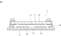
- FIG. 2 is a schematic cross-sectional view of the acoustic wave device according to the second embodiment.
- FIG. 1 is a schematic cross-sectional view of the acoustic wave device according to the first embodiment.
- the acoustic wave device 1 includes a first acoustic wave element 10 and a second acoustic wave element 20.
- the first acoustic wave element 10 includes a first piezoelectric substrate 11 and a first IDT electrode 12 disposed on one main surface 11 a of the first piezoelectric substrate 11.
- the second acoustic wave element 20 includes a second piezoelectric substrate 21 and a second IDT electrode 22 disposed on one main surface 21 a of the second piezoelectric substrate 21.
- the main surface 21 a of the second piezoelectric substrate 21 faces the main surface 11 a of the first piezoelectric substrate 11.
- the first and second piezoelectric substrates 11 and 21 are bonded so that the main surfaces 11a and 21a of the first and second piezoelectric substrates 11 and 21 overlap.
- protrusions or grooves may be provided on the main surfaces 11a and 21a of the first and second piezoelectric substrates 11 and 21.
- the first and second IDT electrodes 12 and 22 are formed by a known method such as sputtering with Al, Pt, Au, Ag, Cu, Ni, Ti, Cr, Pd or an alloy containing at least one of these metals. Can be configured.
- the first and second piezoelectric substrates 11 and 21 can be made of, for example, a material such as LiNbO 3 or LiTaO 3 .
- the first piezoelectric substrate 11 and the second piezoelectric substrate 21 differ in at least one of composition and cut angle.
- the linear expansion coefficient of the second piezoelectric substrate 21 is larger than the linear expansion coefficient of the first piezoelectric substrate 11.
- the acoustic wave device 1 is a duplexer in which one of the first and second acoustic wave elements 10 and 20 constitutes a transmission filter and the other constitutes a reception filter.
- both the first and second acoustic wave elements 10 and 20 may be transmission filters or reception filters.
- the first acoustic wave element 10 is laminated on the main surface of the second acoustic wave element 20.
- the second piezoelectric substrate 21 is disposed on the main surface of the first piezoelectric substrate 11 so as to face the first piezoelectric substrate 11.
- the first piezoelectric substrate 11 and the second piezoelectric substrate 21 are bonded to each other with a bonding layer 30 at intervals. Thereby, a space in which the first and second IDT electrodes 12 and 22 can vibrate is provided.
- the bonding layer 30 can be made of, for example, a resin such as an acrylic resin, a urethane resin, an epoxy resin, a silicone resin, a vinyl acetate resin, or a polyimide resin.
- the linear expansion coefficient of the second piezoelectric substrate 21 is larger than the linear expansion coefficient of the first piezoelectric substrate 11. For this reason, there is a possibility that the temperature cycle resistance is lowered due to the stress generated by the difference in the linear expansion coefficient between the first piezoelectric substrate 11 and the second piezoelectric substrate 21.
- the first substrate 41 having a smaller linear expansion coefficient than the second piezoelectric substrate 21 is bonded to the second piezoelectric substrate 21.
- the material having a small linear expansion coefficient Si, SiO 2 (fused quartz), Al 2 O 3 , Si 3 N 4 , AlN, or the like can be used. For this reason, the difference in the linear expansion coefficient between the first acoustic wave element 10 and the second acoustic wave element 20 is reduced. Thus, excellent temperature cycle resistance is realized.
- a second substrate 42 is provided in addition to the first substrate 41.
- the second substrate 42 is bonded to the first piezoelectric substrate 11.
- the first and second substrates 41 and 42 each have a smaller linear expansion coefficient than that of the first piezoelectric substrate 11. Therefore, the difference in linear expansion coefficient between the first acoustic wave element 10 and the second acoustic wave element 20 is smaller, and the linear expansion coefficient of the first acoustic wave element 10 and the second acoustic wave element 20 are smaller. The coefficient of linear expansion is also reduced. Therefore, more excellent temperature cycle resistance is realized.
- the difference in linear expansion coefficient between the second piezoelectric substrate and the first substrate should be equal to the difference in linear expansion coefficient between the first piezoelectric substrate and the second substrate. Is preferred. Thereby, the difference in change in thermal expansion due to the temperature cycle can be reduced.
- the first and second substrates 41 and 42 have the same composition.
- the first and second substrates 41 and 42 are preferably made of a material having a small coefficient of linear expansion and excellent heat dissipation.
- the first and second substrates 41 and 42 can be made of, for example, sapphire, silicon, or glass.
- the bonding between the first substrate 41 and the second piezoelectric substrate 21 and the bonding between the second substrate 42 and the first piezoelectric substrate 11 are, for example, anodic bonding, eutectic bonding, adhesive bonding, and fusion bonding. , Thermocompression bonding or the like.
- FIG. 2 is a schematic cross-sectional view of the acoustic wave device according to the second embodiment.
- the present invention is not limited to this configuration.
- the first substrate 41 may be provided, and the second substrate 42 may not be provided. Even in this case, the difference in linear expansion coefficient can be reduced similarly, so that excellent temperature cycle resistance can be realized.
- the first substrate 41 may be made of sapphire, silicon, or glass, or may have the same composition as the first piezoelectric substrate 11.
Landscapes
- Physics & Mathematics (AREA)
- Acoustics & Sound (AREA)
- Surface Acoustic Wave Elements And Circuit Networks Thereof (AREA)
- Micromachines (AREA)
Description
図1は、第1の実施形態に係る弾性波装置の略図的断面図である。図1に示されるように、弾性波装置1は、第1の弾性波素子10と、第2の弾性波素子20とを備える。第1の弾性波素子10は、第1の圧電基板11と、第1の圧電基板11の一方主面11a上に配置された第1のIDT電極12とを有する。一方、第2の弾性波素子20は、第2の圧電基板21と、第2の圧電基板21の一方主面21a上に配置された第2のIDT電極22とを有する。第2の圧電基板21の主面21aは、第1の圧電基板11の主面11aと対向している。平面視したとき、第1及び第2の圧電基板11,21の主面11a,21aが重なるように、第1,第2の圧電基板11,21が接合されている。振動可能な空間を設けるために、第1及び第2の圧電基板11,21の主面11a,21a上に突部または溝部を設けてもよい。第1及び第2のIDT電極12,22は、例えば、Al,Pt,Au,Ag,Cu,Ni,Ti,Cr,Pdやそれらの金属の少なくとも一種を含む合金によりスパッタなどの公知な工法により構成することができる。第1及び第2の圧電基板11,21は、例えば、LiNbO3やLiTaO3の材料により構成することができる。本実施形態では、第1の圧電基板11と第2の圧電基板21とで組成及びカット角の少なくとも一方が異なる。第1の圧電基板11の線膨張係数よりも第2の圧電基板21の線膨張係数の方が大きい。
図2は、第2の実施形態に係る弾性波装置の略図的断面図である。
10…第1の弾性波素子
11…第1の圧電基板
12…IDT電極
20…第2の弾性波素子
21…第2の圧電基板
22…第2のIDT電極
30…接合層
41…第1の基板
42…第2の基板
Claims (7)
- 第1の圧電基板を有する第1の弾性波素子と、
前記第1の圧電基板に積層されており、前記第1の圧電基板よりも線膨張係数が大きな第2の圧電基板を有する第2の弾性波素子と、
前記第2の圧電基板に接合されており、前記第2の圧電基板よりも線膨張係数が小さな第1の基板と、
を備える、弾性波装置。 - 前記第1の基板が前記第1の圧電基板と同じ組成を有する、請求項1に記載の弾性波装置。
- 前記第2の圧電基板に接合された第2の基板をさらに備え、
前記第1及び第2の基板のそれぞれは、前記第1の圧電基板よりも小さな線膨張係数を有する、請求項1に記載の弾性波装置。 - 前記第1の基板と前記第2の基板とが同じ組成を有する、請求項3に記載の弾性波装置。
- 前記第1及び第2の基板が、サファイア、シリコンまたはガラスからなる、請求項3または4に記載の弾性波装置。
- 前記第1の圧電基板と前記第2の圧電基板とでは、組成及びカット角の少なくとも一方が異なる、請求項1~5のいずれか一項に記載の弾性波装置。
- 前記第1の弾性波素子は、前記第1の圧電基板の上に設けられた第1のIDT電極をさらに有し、
前記第2の弾性波素子は、前記第2の圧電基板の上に設けられた第2のIDT電極をさらに有する、請求項1~6のいずれか一項に記載の弾性波装置。
Priority Applications (4)
| Application Number | Priority Date | Filing Date | Title |
|---|---|---|---|
| DE112013002924.3T DE112013002924B4 (de) | 2012-08-29 | 2013-07-23 | Bauelement für elastische Wellen |
| JP2014506019A JP5549792B1 (ja) | 2012-08-29 | 2013-07-23 | 弾性波装置 |
| CN201380027452.2A CN104321966B (zh) | 2012-08-29 | 2013-07-23 | 弹性波装置 |
| US14/589,043 US9130539B2 (en) | 2012-08-29 | 2015-01-05 | Elastic wave device with stacked piezoelectric substrates |
Applications Claiming Priority (2)
| Application Number | Priority Date | Filing Date | Title |
|---|---|---|---|
| JP2012-188535 | 2012-08-29 | ||
| JP2012188535 | 2012-08-29 |
Related Child Applications (1)
| Application Number | Title | Priority Date | Filing Date |
|---|---|---|---|
| US14/589,043 Continuation US9130539B2 (en) | 2012-08-29 | 2015-01-05 | Elastic wave device with stacked piezoelectric substrates |
Publications (1)
| Publication Number | Publication Date |
|---|---|
| WO2014034326A1 true WO2014034326A1 (ja) | 2014-03-06 |
Family
ID=50183146
Family Applications (1)
| Application Number | Title | Priority Date | Filing Date |
|---|---|---|---|
| PCT/JP2013/069871 Ceased WO2014034326A1 (ja) | 2012-08-29 | 2013-07-23 | 弾性波装置 |
Country Status (5)
| Country | Link |
|---|---|
| US (1) | US9130539B2 (ja) |
| JP (1) | JP5549792B1 (ja) |
| CN (1) | CN104321966B (ja) |
| DE (1) | DE112013002924B4 (ja) |
| WO (1) | WO2014034326A1 (ja) |
Cited By (5)
| Publication number | Priority date | Publication date | Assignee | Title |
|---|---|---|---|---|
| WO2017110308A1 (ja) * | 2015-12-21 | 2017-06-29 | 株式会社村田製作所 | 弾性波装置 |
| JP2017157922A (ja) * | 2016-02-29 | 2017-09-07 | 太陽誘電株式会社 | 電子デバイス |
| US20180013404A1 (en) * | 2015-06-24 | 2018-01-11 | Murata Manufacturing Co., Ltd. | Elastic wave filter apparatus |
| WO2018123447A1 (ja) * | 2016-12-26 | 2018-07-05 | 株式会社村田製作所 | 弾性波装置、高周波フロントエンドモジュールおよび通信装置 |
| KR20220019098A (ko) * | 2020-08-07 | 2022-02-15 | 스프레드트럼 커뮤니케이션즈 (상하이) 컴퍼니 리미티드 | 웨이퍼 레벨 탄성 표면파 필터와 패키지 방법 |
Families Citing this family (4)
| Publication number | Priority date | Publication date | Assignee | Title |
|---|---|---|---|---|
| DE102015122628B4 (de) | 2015-12-22 | 2018-09-20 | Snaptrack, Inc. | Wafer Level Package und Verfahren zur Herstellung |
| WO2018235876A1 (ja) * | 2017-06-23 | 2018-12-27 | 株式会社村田製作所 | 弾性波装置、フロントエンド回路及び通信装置 |
| KR102490963B1 (ko) * | 2017-12-25 | 2023-01-19 | 가부시키가이샤 무라타 세이사쿠쇼 | 고주파 장치 |
| DE102018108611B4 (de) * | 2018-04-11 | 2019-12-12 | RF360 Europe GmbH | Gehäuse für elektrische Vorrichtung und Verfahren zum Herstellen des Gehäuses |
Citations (5)
| Publication number | Priority date | Publication date | Assignee | Title |
|---|---|---|---|---|
| JP2005191716A (ja) * | 2003-12-24 | 2005-07-14 | Kyocera Corp | 圧電共振子及びフィルタ並びに複合基板 |
| JP2007060465A (ja) * | 2005-08-26 | 2007-03-08 | Seiko Epson Corp | 薄膜弾性表面波デバイス |
| JP2008546207A (ja) * | 2005-06-07 | 2008-12-18 | エプコス アクチエンゲゼルシャフト | 電気的素子および製造方法 |
| JP2011130385A (ja) * | 2009-12-21 | 2011-06-30 | Murata Mfg Co Ltd | 圧電デバイスの製造方法 |
| WO2011102049A1 (ja) * | 2010-02-17 | 2011-08-25 | 株式会社 村田製作所 | 弾性波デバイス |
Family Cites Families (16)
| Publication number | Priority date | Publication date | Assignee | Title |
|---|---|---|---|---|
| JPH11340769A (ja) | 1998-05-22 | 1999-12-10 | Matsushita Electric Ind Co Ltd | ガラス接合圧電基板の製造方法 |
| JP3952666B2 (ja) | 2000-06-23 | 2007-08-01 | 株式会社日立製作所 | 弾性表面波素子 |
| US7105980B2 (en) * | 2002-07-03 | 2006-09-12 | Sawtek, Inc. | Saw filter device and method employing normal temperature bonding for producing desirable filter production and performance characteristics |
| JP3815424B2 (ja) * | 2002-11-08 | 2006-08-30 | 株式会社村田製作所 | 弾性境界波装置 |
| JP3774782B2 (ja) * | 2003-05-14 | 2006-05-17 | 富士通メディアデバイス株式会社 | 弾性表面波素子の製造方法 |
| JP2005033689A (ja) | 2003-07-11 | 2005-02-03 | Toyo Commun Equip Co Ltd | 弾性表面波装置及びその製造方法 |
| DE102004010703B4 (de) | 2004-03-04 | 2015-03-12 | Epcos Ag | Bauelement mit WLP-fähiger Verkapselung und Herstellverfahren |
| JP2006298694A (ja) | 2005-04-20 | 2006-11-02 | Nec Tokin Corp | 圧電複合基板及びその製造方法 |
| JP2007235304A (ja) | 2006-02-28 | 2007-09-13 | Matsushita Electric Ind Co Ltd | 電子部品とその製造方法およびそれを用いた通信機器 |
| EP2104228A4 (en) * | 2006-12-25 | 2014-10-08 | Murata Manufacturing Co | EQUIPMENT WITH ELASTIC RIMS |
| JP2008270901A (ja) | 2007-04-16 | 2008-11-06 | Sony Ericsson Mobilecommunications Japan Inc | 電話端末及び通信システム |
| JP2009094661A (ja) | 2007-10-05 | 2009-04-30 | Hitachi Media Electoronics Co Ltd | 弾性表面波装置及びこれを搭載した移動通信端末 |
| DE102007058951B4 (de) | 2007-12-07 | 2020-03-26 | Snaptrack, Inc. | MEMS Package |
| JP5500966B2 (ja) | 2008-12-25 | 2014-05-21 | 日本碍子株式会社 | 複合基板及び金属パターンの形成方法 |
| KR101661361B1 (ko) * | 2010-01-14 | 2016-09-29 | 엔지케이 인슐레이터 엘티디 | 복합 기판, 및 그것을 이용한 탄성 표면파 필터와 탄성 표면파 공진기 |
| JP2011211331A (ja) | 2010-03-29 | 2011-10-20 | Shin-Etsu Chemical Co Ltd | 複合圧電基板、弾性表面波素子 |
-
2013
- 2013-07-23 DE DE112013002924.3T patent/DE112013002924B4/de active Active
- 2013-07-23 JP JP2014506019A patent/JP5549792B1/ja active Active
- 2013-07-23 WO PCT/JP2013/069871 patent/WO2014034326A1/ja not_active Ceased
- 2013-07-23 CN CN201380027452.2A patent/CN104321966B/zh active Active
-
2015
- 2015-01-05 US US14/589,043 patent/US9130539B2/en active Active
Patent Citations (5)
| Publication number | Priority date | Publication date | Assignee | Title |
|---|---|---|---|---|
| JP2005191716A (ja) * | 2003-12-24 | 2005-07-14 | Kyocera Corp | 圧電共振子及びフィルタ並びに複合基板 |
| JP2008546207A (ja) * | 2005-06-07 | 2008-12-18 | エプコス アクチエンゲゼルシャフト | 電気的素子および製造方法 |
| JP2007060465A (ja) * | 2005-08-26 | 2007-03-08 | Seiko Epson Corp | 薄膜弾性表面波デバイス |
| JP2011130385A (ja) * | 2009-12-21 | 2011-06-30 | Murata Mfg Co Ltd | 圧電デバイスの製造方法 |
| WO2011102049A1 (ja) * | 2010-02-17 | 2011-08-25 | 株式会社 村田製作所 | 弾性波デバイス |
Cited By (14)
| Publication number | Priority date | Publication date | Assignee | Title |
|---|---|---|---|---|
| US20180013404A1 (en) * | 2015-06-24 | 2018-01-11 | Murata Manufacturing Co., Ltd. | Elastic wave filter apparatus |
| US11831300B2 (en) * | 2015-06-24 | 2023-11-28 | Murata Manufacturing Co., Ltd. | Elastic wave filter apparatus |
| US10601399B2 (en) * | 2015-06-24 | 2020-03-24 | Murata Manufacturing Co., Ltd. | Elastic wave filter apparatus |
| US20200212886A1 (en) * | 2015-06-24 | 2020-07-02 | Murata Manufacturing Co., Ltd. | Elastic wave filter apparatus |
| US11695388B2 (en) | 2015-12-21 | 2023-07-04 | Murata Manufacturing Co., Ltd. | Elastic wave device |
| WO2017110308A1 (ja) * | 2015-12-21 | 2017-06-29 | 株式会社村田製作所 | 弾性波装置 |
| JP2017157922A (ja) * | 2016-02-29 | 2017-09-07 | 太陽誘電株式会社 | 電子デバイス |
| WO2018123447A1 (ja) * | 2016-12-26 | 2018-07-05 | 株式会社村田製作所 | 弾性波装置、高周波フロントエンドモジュールおよび通信装置 |
| US11177788B2 (en) | 2016-12-26 | 2021-11-16 | Murata Manufacturing Co., Ltd. | Acoustic wave device, radio frequency front-end module, and communication device |
| JPWO2018123447A1 (ja) * | 2016-12-26 | 2019-10-31 | 株式会社村田製作所 | 弾性波装置、高周波フロントエンドモジュールおよび通信装置 |
| KR20220019098A (ko) * | 2020-08-07 | 2022-02-15 | 스프레드트럼 커뮤니케이션즈 (상하이) 컴퍼니 리미티드 | 웨이퍼 레벨 탄성 표면파 필터와 패키지 방법 |
| JP2022546753A (ja) * | 2020-08-07 | 2022-11-08 | 展訊通信(上海)有限公司 | ウエハレベル弾性表面波フィルタ及びパッケージ方法 |
| JP7449315B2 (ja) | 2020-08-07 | 2024-03-13 | 展訊通信(上海)有限公司 | ウエハレベル弾性表面波フィルタ及びパッケージ方法 |
| KR102843095B1 (ko) * | 2020-08-07 | 2025-08-05 | 스프레드트럼 커뮤니케이션즈 (상하이) 컴퍼니 리미티드 | 웨이퍼 레벨 탄성 표면파 필터와 패키지 방법 |
Also Published As
| Publication number | Publication date |
|---|---|
| DE112013002924B4 (de) | 2016-03-24 |
| JP5549792B1 (ja) | 2014-07-16 |
| DE112013002924T5 (de) | 2015-02-26 |
| CN104321966B (zh) | 2016-03-02 |
| JPWO2014034326A1 (ja) | 2016-08-08 |
| US20150109071A1 (en) | 2015-04-23 |
| US9130539B2 (en) | 2015-09-08 |
| CN104321966A (zh) | 2015-01-28 |
Similar Documents
| Publication | Publication Date | Title |
|---|---|---|
| JP5549792B1 (ja) | 弾性波装置 | |
| JP6519655B2 (ja) | 弾性波装置 | |
| JP6856825B2 (ja) | 弾性波装置、分波器および通信装置 | |
| JP5648695B2 (ja) | 弾性波装置及びその製造方法 | |
| KR102029744B1 (ko) | 탄성파 장치 | |
| JP6481687B2 (ja) | 弾性波装置 | |
| KR102111928B1 (ko) | 탄성파 장치 | |
| JP6397352B2 (ja) | 弾性波デバイス | |
| KR101636220B1 (ko) | 복합 기판, 압전 디바이스 및 복합 기판의 제법 | |
| WO2017043427A1 (ja) | 弾性波装置、高周波フロントエンド回路及び通信装置 | |
| KR101661361B1 (ko) | 복합 기판, 및 그것을 이용한 탄성 표면파 필터와 탄성 표면파 공진기 | |
| JP6854891B2 (ja) | 弾性波装置、分波器および通信装置 | |
| WO2011158636A1 (ja) | 複合基板 | |
| JP2019179961A (ja) | 弾性波装置 | |
| JP2017011681A (ja) | 弾性波装置 | |
| JP6835220B2 (ja) | 弾性波装置、フロントエンド回路及び通信装置 | |
| WO2015178227A1 (ja) | 弾性波デバイス及びその製造方法 | |
| JP2015122566A (ja) | 弾性波装置 | |
| JP6488667B2 (ja) | 表面弾性波デバイス | |
| JP5458651B2 (ja) | 弾性表面波素子用基板及び弾性表面波素子の製造方法 | |
| JP2009278422A (ja) | 弾性表面波デバイス及びその製造方法 | |
| JP2008211277A (ja) | 弾性表面波素子 | |
| JP6920161B2 (ja) | 弾性波デバイスおよび複合基板 | |
| JP2011071838A (ja) | 弾性表面波素子 | |
| JP2011109481A (ja) | 弾性波デバイスおよびその製造方法 |
Legal Events
| Date | Code | Title | Description |
|---|---|---|---|
| ENP | Entry into the national phase |
Ref document number: 2014506019 Country of ref document: JP Kind code of ref document: A |
|
| 121 | Ep: the epo has been informed by wipo that ep was designated in this application |
Ref document number: 13832922 Country of ref document: EP Kind code of ref document: A1 |
|
| WWE | Wipo information: entry into national phase |
Ref document number: 112013002924 Country of ref document: DE Ref document number: 1120130029243 Country of ref document: DE |
|
| 122 | Ep: pct application non-entry in european phase |
Ref document number: 13832922 Country of ref document: EP Kind code of ref document: A1 |