WO2014034252A1 - 欠陥観察システムおよび欠陥観察方法 - Google Patents
欠陥観察システムおよび欠陥観察方法 Download PDFInfo
- Publication number
- WO2014034252A1 WO2014034252A1 PCT/JP2013/067969 JP2013067969W WO2014034252A1 WO 2014034252 A1 WO2014034252 A1 WO 2014034252A1 JP 2013067969 W JP2013067969 W JP 2013067969W WO 2014034252 A1 WO2014034252 A1 WO 2014034252A1
- Authority
- WO
- WIPO (PCT)
- Prior art keywords
- magnification
- defect
- image
- field
- view
- Prior art date
- Legal status (The legal status is an assumption and is not a legal conclusion. Google has not performed a legal analysis and makes no representation as to the accuracy of the status listed.)
- Ceased
Links
Images






Classifications
-
- G—PHYSICS
- G06—COMPUTING OR CALCULATING; COUNTING
- G06T—IMAGE DATA PROCESSING OR GENERATION, IN GENERAL
- G06T7/00—Image analysis
- G06T7/0002—Inspection of images, e.g. flaw detection
- G06T7/0004—Industrial image inspection
- G06T7/001—Industrial image inspection using an image reference approach
-
- H—ELECTRICITY
- H01—ELECTRIC ELEMENTS
- H01J—ELECTRIC DISCHARGE TUBES OR DISCHARGE LAMPS
- H01J37/00—Discharge tubes with provision for introducing objects or material to be exposed to the discharge, e.g. for the purpose of examination or processing thereof
- H01J37/02—Details
- H01J37/22—Optical, image processing or photographic arrangements associated with the tube
-
- H—ELECTRICITY
- H01—ELECTRIC ELEMENTS
- H01J—ELECTRIC DISCHARGE TUBES OR DISCHARGE LAMPS
- H01J37/00—Discharge tubes with provision for introducing objects or material to be exposed to the discharge, e.g. for the purpose of examination or processing thereof
- H01J37/02—Details
- H01J37/22—Optical, image processing or photographic arrangements associated with the tube
- H01J37/222—Image processing arrangements associated with the tube
-
- H—ELECTRICITY
- H01—ELECTRIC ELEMENTS
- H01J—ELECTRIC DISCHARGE TUBES OR DISCHARGE LAMPS
- H01J37/00—Discharge tubes with provision for introducing objects or material to be exposed to the discharge, e.g. for the purpose of examination or processing thereof
- H01J37/26—Electron or ion microscopes; Electron or ion diffraction tubes
- H01J37/28—Electron or ion microscopes; Electron or ion diffraction tubes with scanning beams
-
- G—PHYSICS
- G01—MEASURING; TESTING
- G01N—INVESTIGATING OR ANALYSING MATERIALS BY DETERMINING THEIR CHEMICAL OR PHYSICAL PROPERTIES
- G01N23/00—Investigating or analysing materials by the use of wave or particle radiation, e.g. X-rays or neutrons, not covered by groups G01N3/00 – G01N17/00, G01N21/00 or G01N22/00
- G01N23/22—Investigating or analysing materials by the use of wave or particle radiation, e.g. X-rays or neutrons, not covered by groups G01N3/00 – G01N17/00, G01N21/00 or G01N22/00 by measuring secondary emission from the material
- G01N23/225—Investigating or analysing materials by the use of wave or particle radiation, e.g. X-rays or neutrons, not covered by groups G01N3/00 – G01N17/00, G01N21/00 or G01N22/00 by measuring secondary emission from the material using electron or ion
-
- G—PHYSICS
- G06—COMPUTING OR CALCULATING; COUNTING
- G06T—IMAGE DATA PROCESSING OR GENERATION, IN GENERAL
- G06T2207/00—Indexing scheme for image analysis or image enhancement
- G06T2207/10—Image acquisition modality
- G06T2207/10056—Microscopic image
- G06T2207/10061—Microscopic image from scanning electron microscope
-
- H—ELECTRICITY
- H01—ELECTRIC ELEMENTS
- H01J—ELECTRIC DISCHARGE TUBES OR DISCHARGE LAMPS
- H01J2237/00—Discharge tubes exposing object to beam, e.g. for analysis treatment, etching, imaging
- H01J2237/22—Treatment of data
- H01J2237/221—Image processing
-
- H—ELECTRICITY
- H01—ELECTRIC ELEMENTS
- H01J—ELECTRIC DISCHARGE TUBES OR DISCHARGE LAMPS
- H01J2237/00—Discharge tubes exposing object to beam, e.g. for analysis treatment, etching, imaging
- H01J2237/244—Detection characterized by the detecting means
- H01J2237/2448—Secondary particle detectors
-
- H—ELECTRICITY
- H01—ELECTRIC ELEMENTS
- H01J—ELECTRIC DISCHARGE TUBES OR DISCHARGE LAMPS
- H01J2237/00—Discharge tubes exposing object to beam, e.g. for analysis treatment, etching, imaging
- H01J2237/245—Detection characterised by the variable being measured
- H01J2237/24592—Inspection and quality control of devices
-
- H—ELECTRICITY
- H01—ELECTRIC ELEMENTS
- H01J—ELECTRIC DISCHARGE TUBES OR DISCHARGE LAMPS
- H01J2237/00—Discharge tubes exposing object to beam, e.g. for analysis treatment, etching, imaging
- H01J2237/26—Electron or ion microscopes
- H01J2237/28—Scanning microscopes
- H01J2237/2803—Scanning microscopes characterised by the imaging method
- H01J2237/2806—Secondary charged particle
-
- H—ELECTRICITY
- H01—ELECTRIC ELEMENTS
- H01J—ELECTRIC DISCHARGE TUBES OR DISCHARGE LAMPS
- H01J2237/00—Discharge tubes exposing object to beam, e.g. for analysis treatment, etching, imaging
- H01J2237/26—Electron or ion microscopes
- H01J2237/28—Scanning microscopes
- H01J2237/2813—Scanning microscopes characterised by the application
- H01J2237/2817—Pattern inspection
Definitions
- the present invention relates to a defect observation system and a program used in the defect observation system.
- the SEM (Scanning / Electron / Microscope) type defect observation apparatus is an apparatus for observing such various defects.
- an image of defect coordinates detected by an upper defect inspection apparatus is higher than that of the upper defect inspection apparatus. It is a device for observing with image quality.
- the sample stage is moved to the defect coordinates output by the higher-level defect inspection device, and the defect to be observed is imaged at a low magnification so that the defect enters the field of view.
- the coordinate stage is detected, and the sample stage is moved so that the defect is positioned at the center of the visual field, or the imaging center is moved, and a high-magnification image for observation is acquired at a high magnification suitable for defect observation.
- the reason why the defect coordinates are detected in the low-magnification image is that the defect coordinates output from the upper defect inspection apparatus include an error within the range of the apparatus specifications. When acquiring a high-quality defect image, it is necessary to correct this error.
- ADR Automatic Defect Review or Redetection
- the characteristics of the sample, and the type of defect to be observed, the low-magnification image acquisition condition for detecting the defect, and the high magnification for analyzing the defect Image acquisition conditions and the like need to be optimized in order to achieve both ADR defect detection rate and throughput.
- ADC Automatic Defect Classification
- ADC Automatic Defect Classification
- Patent Document 1 discloses a technique for executing an autofocus process outside the range of the field of view of a defect image so that contamination generated during the autofocus process does not adversely affect the defect image.
- Patent Document 1 If the technique disclosed in Patent Document 1 is used, a defect image can be acquired without being affected by the contamination that occurs during autofocusing. However, in ADR, a low-magnification image used for defect detection can be acquired. The effects of contamination and local charging that occur during acquisition cannot be avoided.
- An object of the present invention is to provide a defect observation system capable of performing defect detection and defect classification processing with high accuracy even when contamination or local charging may occur during low-magnification image acquisition. It is.
- the configuration described in the claims is adopted.
- the present application includes a plurality of means for solving the above-mentioned problems.
- the field of view of the high-magnification image or the low-magnification image is such that the outer edge portion of the field of view of the low-magnification image is not included in the field of view of the high-magnification image. Is set.
- the present invention it is possible to provide a defect observation system capable of performing highly accurate defect detection and defect classification processing even when contamination or local charging may occur during low-magnification image acquisition. Can do.
- the schematic block diagram of a SEM type defect observation system The block diagram of the operation and analysis part of a SEM type defect observation system. Schematic diagram of high-magnification imaging when the influence of contamination and local charging can be ignored. Schematic diagram of high-magnification imaging when the influence of contamination and local charging cannot be ignored.
- the high magnification imaging schematic diagram which optimizes the high magnification visual field center.
- the ADR flowchart which optimizes a high magnification visual field center.
- the high magnification imaging schematic diagram which optimizes a high magnification visual field size.
- FIG. 1 Schematic diagram of high-magnification imaging that optimizes the low-magnification field size.
- the ADR flowchart which optimizes a low magnification visual field size.
- the ADR flowchart which updates a low magnification visual field size at the time of a review.
- the functional block diagram which sets an observation visual field.
- a configuration example of an SEM type defect observation system having a function of acquiring a high-magnification image so that a contamination and a boundary of local charging that occur at the time of acquisition of the low-magnification image do not enter the high-magnification image will be described.
- the defect observation system described below is merely an example of the present invention, and the present invention is not limited to the embodiment described below.
- the defect observation system is an apparatus that captures an image of a sample using a charged particle beam, and widely includes apparatuses that capture an image at a plurality of different magnifications.
- the system configuration is not limited to this, and part or all of the devices constituting the defect observation system May be composed of different devices.
- the ADR processing of the present embodiment may be performed by a recipe management device or an image management device connected to the SEM type defect observation device over a network, or a CPU (Central Processing Unit) mounted on a general-purpose computer in the system
- the program may be executed by a program that executes a desired calculation process. It is also possible to upgrade an existing apparatus with a storage medium in which this program is recorded.
- defects are not limited to pattern defects, but include a wide range of objects to be observed such as foreign matters, pattern dimension abnormalities, and structural defects.
- the SEM observation device is a defect coordinate detected by a defect inspection device such as an optical or SEM inspection device as input information, and a high-quality SEM image of the defect coordinate or the observation coordinate under conditions suitable for observation and analysis. It is a device to acquire.
- a defect inspection device such as an optical or SEM inspection device
- a high-quality SEM image of the defect coordinate or the observation coordinate under conditions suitable for observation and analysis It is a device to acquire.
- coordinate information of observation points extracted by simulation based on design layout data can be used as input information to the SEM observation apparatus.
- FIG. 1 is a schematic diagram showing the overall configuration of the SEM observation system in the present example.
- the SEM type defect observation apparatus 118 in FIG. 1 includes an electron optical system composed of optical elements such as an electron gun 101, a lens 102, a scanning deflector 103, an objective lens 104, a sample 105, a secondary particle detector 109, and an observation target.
- the stage 106 that moves the sample stage that holds the sample to be in the XY plane, the electron optical system control unit 110 that controls various optical elements included in the electron optical system, and the output signal of the secondary particle detector 109
- An A / D conversion unit 111 that performs quantization
- a stage control unit 112 that controls the stage 106
- an overall control / analysis unit 113 an image processing unit 114
- an operation unit 115 including a display, a keyboard, and a mouse, an acquired image, and the like.
- a storage device 116 to be held, an optical microscope 117, and the like are included.
- the electron optical system, the electron optical system control unit 110, the A / D conversion unit 111, the stage 106, and the stage control unit 112 constitute a scanning electron microscope that is an imaging unit for SEM images.
- the primary electron beam 107 emitted from the electron gun 101 is converged by the lens 102, deflected by the scanning deflector 102, converged by the objective lens 104, and irradiated on the sample 105.
- secondary particles 108 such as secondary electrons and reflected electrons are generated according to the shape and material of the sample.
- the generated secondary particles 108 are detected by the secondary particle detector 109 and then converted into a digital signal by the A / D converter 111.
- the output signal of the secondary particle detector converted into a digital signal may be referred to as an image signal.
- the output signal of the A / D conversion unit 111 is output to the image processing unit 114 to form an SEM image.
- the image processing unit 114 uses the generated SEM image to perform various image analysis processes such as an ADR process that performs image processing such as defect detection and an ADC process that automatically classifies defects by type.
- the SEM observation apparatus can acquire an image of an observation target area at a plurality of different magnifications. For example, it is possible to change the magnification by changing the scanning range of the scanning deflector 103 for observation.
- Control of the optical elements inside the electron optical system such as the lens 102, the scanning deflector 103, and the objective lens 104 is executed by the electron optical system control unit 110.
- the sample position control is executed by the stage 106 controlled by the stage control unit 112.
- the overall control / analysis unit 113 is a control unit that comprehensively controls the entire SEM observation apparatus, interprets input information from the operation unit 115 and the storage device 116 including a display, a keyboard, a mouse, and the like, and
- the optical system control unit 110, the stage control unit 112, the image processing unit 114, and the like are controlled, and processing results are output to the display unit 206 and the storage device 116 included in the operation unit 115 as necessary.
- the processing executed by the image processing unit 114 can be realized by either hardware or software. When executed by hardware, it can be realized by integrating a plurality of arithmetic units for executing processing in a wiring board, a semiconductor chip, or a package. When configured by software, it can be realized by installing a high-speed CPU in the image processing unit 114 and executing desired arithmetic processing by a program.
- FIG. 1 shows an example in which an SEM type defect observation apparatus 118, a recipe management apparatus 120, and a defect information database 121 are connected via a LAN (Local Area Network) 119 as an example of the defect observation system.
- the image acquired by the SEM type defect observation apparatus 118 is stored in the defect information database 121.
- information related to defects for example, defect image acquisition conditions and detected defect coordinates are also stored in the defect information database 121.
- the recipe management device 120 acquires defect information necessary for recipe creation from the defect information database 121, performs arithmetic processing including image processing, and creates a recipe.
- the parameters used for the arithmetic processing, the created recipe, and the like may be stored in a storage device built in the recipe management device, or may be stored in a defect information database.
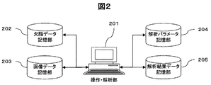
- FIG. 2 shows a detailed view of the overall control unit and the analysis unit 113 of FIG.
- An operation / analysis unit 201 illustrated in FIG. 2 is an integrated representation of the overall control / analysis unit 113 and the operation unit 115 illustrated in FIG. 1, and the overall control / analysis unit 113 is operated in response to an operation instruction from the operation unit 115.
- the CPU incorporated in is implemented by a plurality of functional blocks that are realized by executing a predetermined program.
- the overall control / analysis unit as shown in FIG. 1 is not limited to the configuration incorporated in the SEM observation apparatus, and the operation shown in FIG. 2 is independent of the SEM observation apparatus shown in FIG. -
- the analysis part 201 may be comprised and the component of FIG. 1 and FIG. 2 may be connected by network connection.
- the defect data storage unit 202, the image data storage unit 203, the analysis parameter storage unit 204, and the analysis result data storage unit 205 are integrated into the storage device 116 of FIG. May be.
- the defect data storage unit 201 stores defect information such as defect coordinates.
- the image data storage unit 202 stores defect images captured by the SEM observation apparatus.
- the analysis parameter storage unit 204 stores conditions such as an ADR condition and an ADC condition executed during image acquisition and image analysis, and a plurality of conditions can be reproduced.
- the processing result is stored in the analysis result data storage unit 205.
- the function of the operation / analysis unit 201 can be realized by the recipe management device 120 in the SEM type defect observation system shown in FIG.
- the defect data storage unit 202, the image data storage unit 203, the analysis parameter storage unit 204, and the analysis result data storage unit 205 can also be realized by the defect information database 121 in the SEM type defect observation system shown in FIG.
- FIG. 3 is a schematic diagram showing a situation in which a high-magnification image is acquired when the influence of contamination and local charging that occur during acquisition of a low-magnification image can be ignored, and is an example in which a conventional technique is employed.
- a low-magnification image is obtained by irradiating the region of the low-magnification visual field 302 with a primary electron beam onto the sample 301 to be observed.
- the SEM type observation apparatus acquires a low-magnification image with the coordinates of the defect position output from the higher-level inspection apparatus or the coordinates of the position to be observed obtained by simulation as the center of the visual field.
- the example of FIG. 3 is an example of observing a defect detected by a host inspection device.
- the defect in an ideal state where the defect detection accuracy of the host inspection device is good and the stage accuracy of the SEM observation device is good, the defect is Is located in the center of the low magnification field of view.
- the defect detection accuracy of the upper inspection apparatus is often in the order of microns, so the low magnification image is set so that the low magnification field of view is set to several microns and the defect enters the low magnification field of view. It is often set with a lower magnification.
- defect coordinates are detected from the low-magnification image, and a high-magnification image 304 is obtained with a desired high-magnification field 303 using the detected defect coordinates as the center of the high-magnification field of view.
- This procedure is automated by ADR, and it is common to detect defect coordinates by comparing a low-magnification defect image in which a defect is located in the field of view with a low-magnification reference image in which no defect is present in the field of view. It is used for.
- the high-magnification visual field 303 is set to an appropriate size according to the analysis content using the acquired high-magnification image 304.
- the size of the high-magnification field of view is input by the user or automatically set according to the analysis content, and is registered in a recipe that represents the inspection conditions.
- FIG. 4 shows a problem of the prior art that occurs when a high-magnification image is obtained under the same conditions as in FIG. 3 when the influence of contamination or local charging that occurs when the low-magnification image is obtained cannot be ignored.
- the image quality changes due to contamination caused by electron beam irradiation or the influence of local charging but the cause of the image quality change is not limited to this and may be other causes.
- a low-magnification image is obtained by irradiating the region 401 of the low-magnification visual field 402 with respect to the sample 401 to be observed, with a primary electron beam.
- the material of the sample, contamination and local charging may be noticeable.
- the importance of analyzing minute defects increases as the manufacturing pattern becomes finer and the manufacturing process becomes more complex, it is necessary to reduce the noise of the low-magnification image and obtain a high-quality defect image.
- the cumulative number is increased, and the opportunity to acquire images is increasing under conditions that are easily affected by contamination and local charging.
- the high-magnification image 404 When the high-magnification image 404 is acquired so that the defect is positioned at the center of the high-magnification field 403 under the condition that the contamination and the local electrification are conspicuous as in the case of FIG. 4, the influence 405 of the contamination and the local electrification is obtained.
- the boundary between the received portion and the unreceived portion, that is, the outer edge of the low-magnification image enters the high-magnification field of view, and the difference in appearance appears between the portion that is not affected by contamination and local charging and the portion that is not affected.
- a high-magnification image is acquired so that the defect is positioned at the center of the high-magnification image.
- a contamination or a boundary of local charging that occurs during acquisition of the low-magnification image may enter the high-magnification image.
- a defect is detected from the outer edge of the low-magnification image to an area inside the half of the length of one side of the field of the high-magnification image (outside 406 in FIG. 4 and inside the outer edge of the low-magnification field 402), Such a problem arises because part of the field of view is an area that is not included in the low magnification field of view.
- the defect feature amount can be determined using ADR or ADC processing.
- ADC the defect image is analyzed, the defect feature is quantified, and the defect type is specified based on the quantified feature amount. Therefore, the defect image is acquired under the condition that the defect feature can be stably quantified. is important. In a situation where the defect image is affected by contamination or local charging, the defect feature value calculation becomes unstable and the classification result is not stable, so the defect image is acquired so that it is not affected by contamination. It is hoped to do.
- view field and “view field range” mean an area included in an output image
- view field size means its size.
- the inner and outer boundaries of the visual field are referred to as “the outer edge of the visual field”, and “within the visual field” means inside the outer edge of the visual field.
- the “field center” means the center position of the field of view. The field of view will be described assuming that it is a square unless otherwise specified, but the present invention is not limited to this, and the field of view may be rectangular, for example.
- FIG. 5 is a schematic diagram for explaining a method for acquiring a high-magnification image of the present embodiment. Similar to FIGS. 3 and 4, the sample 501 to be observed is irradiated with a primary electron beam to the region of the low-magnification visual field 502 to obtain a low-magnification image. Thereafter, defect detection is performed by comparing the acquired low-magnification image (that is, the image to be inspected) with an image of a region having a pattern corresponding to the pattern of the low-magnification image and having no defect.
- Defect detection uses other methods, for example, using the periodicity of the background pattern in the acquired defect image to synthesize an image that does not have a defect, and compares the synthesized image with the defect image to detect the defect. Or a method of comparing the reference data generated from the design data with the defect image may be used.
- images and data to be compared with images to be inspected in defect detection are collectively referred to as reference images.
- the center position of the high-magnification field 503 is controlled so that the high-magnification field is within the low-magnification field.
- the field of view of the high-magnification image so that the outer edge of the low-magnification image is not included in the high-magnification image, contamination and local charge boundaries that occur during acquisition of the low-magnification image can enter the high-magnification image. It is preventing.
- the x direction component of the protrusion amount of the high magnification field 505 in the conventional method is ⁇ x (507), and the y direction component is ⁇ y (508), from the detected defect coordinates (x, y).
- a high-magnification image is obtained with the coordinates obtained by shifting the protrusion amount ( ⁇ x, ⁇ y) in the center direction of the low-magnification visual field as the center of the high-magnification visual field 503.
- ⁇ x and ⁇ y are the origin of the low magnification field (0, 0), the defect coordinates detected from the low magnification image (x, y), the low magnification field size (FOV Low_x , FOV Low_y ), and the high magnification field size (FOV) High_x , FOV High_y ) can be calculated from equations (1) and (2).
- ⁇ x and ⁇ y are one side of the outer edge of the high-magnification image when acquiring a high-magnification image centered on the position of the defect, and one side that is not included in the field-of-view range of the low-magnification image and the outer edge of the low-magnification image Represents the distance in the x and y directions of the closest side of the. Note that the field of view of the high-magnification image may be moved in the direction of the center of the low-magnification field by ⁇ x and ⁇ y or more, but it is necessary that the defect is included in the high-magnification image.
- FIG. 5 shows an example in which neither ⁇ x nor ⁇ y is 0, but the above method can be similarly applied when either one is 0 as a matter of course.
- the high-magnification image 504 in which the boundary of contamination and local charging is not included in the field of image is obtained.
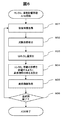
- FIG. 6 is a flowchart when the method described with reference to FIG. 5 is applied to ADR.
- a low-magnification image is acquired with the defect coordinates detected by the host inspection apparatus as input information and the defect coordinates as the center of the visual field (601).
- Defect coordinates are detected from the acquired low-magnification image (602).
- any method may be used to detect the defect coordinates.
- the amount of protrusion ( ⁇ x, ⁇ y) defined in FIG. 5 is calculated (603), and the boundary of contamination and local charging that occurred during acquisition of the low-magnification image, that is, the outer edge of the low-magnification image enters the high-magnification image.
- the center of the high-magnification field of view is set by moving the inside of the low-magnification field of view by the amount of protrusion (604).
- a high-magnification image is acquired based on the set high-magnification field of view (605). A series of these processes is executed for all samples to be observed (606).
- FIG. 7 is a schematic diagram illustrating a second high-magnification image acquisition method according to this embodiment.
- a primary electron beam is irradiated to the region of the low magnification visual field 702 with respect to the sample 701 to be observed to acquire a low magnification image.
- the x-direction component of the protrusion amount of the high-magnification fields 705 and 706 in the conventional method with respect to the low-magnification field 702 is defined as ⁇ x (707), and the y-direction component is defined as ⁇ y (708).
- the size of the high magnification field of view is reduced to 703 by (2 ⁇ ⁇ x, 2 ⁇ ⁇ y) so that the defect is positioned at the center of the high magnification image, and the high magnification image 704 is centered on the detected defect coordinates.
- the size of “(2 ⁇ ⁇ x, 2 ⁇ ⁇ y)” is within the field of view of the high-magnification image determined by the field-of-view size of the high-magnification image designated in advance with the position of the defect as the center, and This is a region not included in the field of view of the low magnification image.
- the field of view of the high-magnification image specified in advance may be input information set by the operator, or the defect occupancy ratio of the high-magnification image is set to be a certain level or more based on the defect size calculated from the low-magnification image. It may be a field of view.
- a high-magnification image is acquired so that a contamination or a local charge boundary generated when acquiring a low-magnification image is prevented from entering the high-magnification image, and a defect is positioned at the center of the high-magnification image. be able to.
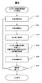
- FIG. 8 is a flowchart when the method described with reference to FIG. 7 is applied to ADR.
- a low-magnification image is acquired using the defect coordinates detected by the host inspection apparatus as input information and the defect coordinates as the center of the field of view (801).
- Defect coordinates are detected from the acquired low-magnification image (802).
- any method may be used to detect the defect coordinates.
- the amount of protrusion ( ⁇ x, ⁇ y) defined in FIG. 5 is calculated (803), so that the contamination and the boundary of the local charge generated at the time of low-magnification image acquisition, that is, the outer edge of the low-magnification image do not enter.
- the field size is reduced by twice the protrusion amount, and a high magnification field is set with the detected defect coordinates as the center of the field (804). Based on the set high magnification field of view, a high magnification image is acquired (805). A series of these processes is executed for all samples to be observed (806).
- a contamination or a boundary of local charging that has occurred during acquisition of the low-magnification image is prevented from entering the high-magnification image, and the center of the high-magnification image is further reduced.
- a high-magnification image can be acquired so that the defect is located in the area.
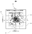
- FIG. 9 is a schematic diagram showing the relationship between a low magnification field obtained from the defect coordinate accuracy of the host inspection apparatus and a low magnification field obtained from the field size of the high magnification image.
- the defect coordinate accuracy of the upper inspection apparatus can be obtained from the amount of deviation between the defect coordinates of the upper inspection apparatus and the defect coordinates redetected by the SEM observation apparatus, and the size of the low magnification field of view can be set from this defect coordinate accuracy. Specifically, for example, if one side of the visual field size of the low-magnification image is at least twice as long as the maximum value of the shift amount, the low-magnification image field of view is entered even in the case of the maximum shift amount. Therefore, the low magnification field of view can be set so that all the defects are in the low magnification field of view.
- the method for setting the low magnification field of view is not limited to this method.
- the variance value ⁇ of the deviation amount is obtained and based on the variance value ⁇ A low magnification field of view may be set.
- the detected defect coordinates are set as the center of the high magnification field.
- a range 905 of a high magnification field to be obtained is obtained.
- a range obtained by adding 1/2 of the high-magnification field size set by the user to the four sides of the low-magnification field of view is a range of the high-magnification field that can be taken when the defect coordinates are set to the center of the high-magnification field of view. It becomes.
- the range of the high magnification field that can be taken when the defect coordinates are set to the center of the high magnification field of view is the length of one side of the field of view determined based on the coordinate accuracy of the defect inspection apparatus. It can be said that it is a range in which a length longer than one side is added and this length is one side. This range is indicated at 905.
- the high magnification field size set by the user has been described.
- ADR automatically sets the high magnification field size based on the detected defect size
- the maximum magnification that can be automatically set is set. What is necessary is just to obtain
- FIG. 10 shows that the boundary of contamination and local charge generated when acquiring a low-magnification image is prevented from entering the high-magnification image, and a high-magnification field of view is desired so that a defect is positioned at the center of the high-magnification image.
- It is a schematic diagram of the acquisition method of the high magnification image which can be maintained to the size of.
- the range of the high magnification field that can be taken when the defect coordinates are set to the center of the high magnification field of view is the field of view of the low magnification image that is actually irradiated with the primary electron beam.
- the low-magnification field size 1002 obtained from the defect coordinate accuracy of the upper inspection apparatus is taken into consideration by taking into consideration the size of the high-magnification field 1003 and the low-magnification obtained from the range that the high magnification field can take.
- a double field of view 1005 is set.
- a low-magnification image is obtained by irradiating a primary electron beam to the low-magnification field 1005 obtained from the range that the high-magnification field can take.
- the high-magnification image 1004 can be acquired with a desired high-magnification field size.
- the low magnification field of view 1002 obtained from the defect coordinate accuracy of the upper inspection apparatus is obtained based on the past results and does not guarantee the future defect coordinate accuracy, so the defect observation was actually performed. In this case, there is a possibility that the defect is located outside the low magnification field 1002 obtained from the defect coordinate accuracy.
- the defect is located outside the low-magnification field of view 1002 obtained from the defect coordinate accuracy, the contamination and local charge boundaries generated during the acquisition of the low-magnification image using the method described in FIGS. You will enter the image.
- a method of limiting the defect detection processing range inside the low-magnification field of view 1002 obtained from the defect coordinate accuracy of the host inspection apparatus may be used. That is, of the actual electron beam irradiation region at a low magnification obtained from the range that can be taken by the high magnification field, only the region within the low magnification field obtained from the coordinate accuracy of the inspection apparatus is set as a target region for defect detection processing. According to this method, the boundary of contamination and local charging that occurred during low-magnification image capture does not enter the high-magnification image, and the defect is located at the center of the high-magnification image, and further, the desired high-magnification field of view.
- a high-magnification image 1004 can be stably acquired by size.
- FIG. 11 is a flowchart when the method described in FIG. 10 is applied to ADR.
- the primary electron beam is It is set as a low magnification field for irradiation (1101).
- a low-magnification image is acquired based on the set low-magnification visual field (1102).
- Defect coordinates are detected from the acquired low-magnification image (1103). As described above, any method may be used to detect the defect coordinates. Further, as described with reference to FIG. 10, the defect detection range may be limited to the inside of the low magnification field obtained from the defect coordinate accuracy of the host inspection apparatus. Next, a high-magnification image is acquired with the detected defect coordinates as the center of the high-magnification visual field (1104). This series of processing is executed for all samples (1105).
- the high-magnification image does not have a contamination or local charge boundary at the time of low-magnification imaging, and the defect is located at the center of the high-magnification image. Can obtain high-magnification images.
- FIG. 12 is an ADR flowchart for updating the actual data for obtaining the defect coordinate accuracy of the host inspection apparatus and the low-magnification visual field size obtained from the actual data at the time of review.
- a low-magnification visual field size is set from the record data of defect coordinate accuracy of the host inspection apparatus (1201). As described with reference to FIGS. 10 and 11, the low magnification field size may be set in consideration of the high magnification field size.
- ⁇ Acquire a low-magnification image based on the set low-magnification field size (1202). Defect coordinates are detected from the acquired low-magnification image (1203). As described above, any method may be used to detect the defect coordinates. When the method described with reference to FIGS. 10 and 11 is employed, the defect detection range may be limited to the inside of the low magnification field determined from the defect coordinate accuracy of the host inspection apparatus.
- the deviation amount of the defect coordinates detected by the host inspection apparatus is obtained from the detected defect coordinates, the newly obtained deviation amount is added to the deviation amount actual data, and the deviation amount actual data is updated (1204).
- a high-magnification image is acquired with the detected defect coordinates as the center of the high-magnification visual field (1205). This series of processing is executed for all the samples to be observed (1206).
- FIG. 13 is a functional block diagram of the observation visual field setting process in the embodiment described so far.
- the observation visual field setting processing block 1301 includes a defect detection processing unit 1302, a deviation amount calculation processing unit 1303, and an observation visual field setting unit 1304.
- the observation visual field processing block 1301 can be implemented in the overall control unit and analysis unit 113 in FIG. 1, the recipe management device 120, the operation / analysis unit 201 in FIG.
- the defect detection processing unit 1302 calculates the defect coordinates 1306 using the defect image 1302 as an input.
- the deviation amount calculation processing unit 1303 receives the defect coordinates 1306 and the inspection coordinates 1307 and outputs a difference between them as a deviation amount 1308.
- the observation visual field setting unit 1304 calculates and sets the observation visual field 1309 of the high-magnification image by using the shift amount 1308 and, if present, the set visual field size 1309 as inputs.
- a portion where contamination or local charging occurs during acquisition of a low-magnification image and a portion where contamination or local charging does not occur are mixed. Therefore, it is possible to provide a defect observation system capable of performing defect detection and defect classification processing with high accuracy.
- this invention is not limited to the above-mentioned Example, Various modifications are included.
- the above-described embodiments have been described in detail for easy understanding of the present invention, and are not necessarily limited to those having all the configurations described.
- a part of the configuration of one embodiment can be replaced with the configuration of another embodiment, and the configuration of another embodiment can be added to the configuration of one embodiment.
- Each of the above-described configurations, functions, processing units, processing means, and the like may be realized by hardware by designing a part or all of them with, for example, an integrated circuit.
- Each of the above-described configurations, functions, and the like may be realized by software by interpreting and executing a program that realizes each function by the processor.
- Information such as programs, tables, and files for realizing each function can be stored in a memory, a hard disk, a recording device such as an SSD (Solid State Drive), or a recording medium such as an IC card, an SD card, or a DVD.
- a recording device such as an SSD (Solid State Drive)
- a recording medium such as an IC card, an SD card, or a DVD.
- control lines and information lines indicate what is considered necessary for the explanation, and not all the control lines and information lines on the product are necessarily shown. Actually, it may be considered that almost all the components are connected to each other.
- 101 electron gun, 102: lens, 103: scanning deflector, 104: objective lens, 105: sample, 106: stage, 107: primary electron beam, 108: secondary particles, 109: secondary particle detector, 110: Electron optical system control unit, 111: A / D conversion unit, 112: stage control unit, 113: overall control / analysis unit, 114: image processing unit, 115: operation unit, 116: storage device, 117: optical microscope, 118 : SEM type defect observation device, 119: LAN, 120: Recipe management device, 121: Defect information database, 201: Operation / analysis unit, 202: Defect data storage unit, 203: Image data storage unit, 204: Analysis parameter storage unit 205: analysis result storage unit, 301: sample, 302: low magnification field of view, 303: high magnification field of view, 304: high magnification image, 401: sample, 402: low magnification field of view, 03: High magnification field of view, 404: High mag
Landscapes
- Chemical & Material Sciences (AREA)
- Analytical Chemistry (AREA)
- Engineering & Computer Science (AREA)
- Computer Vision & Pattern Recognition (AREA)
- Physics & Mathematics (AREA)
- General Physics & Mathematics (AREA)
- Quality & Reliability (AREA)
- Theoretical Computer Science (AREA)
- Testing Or Measuring Of Semiconductors Or The Like (AREA)
- Analysing Materials By The Use Of Radiation (AREA)
- Health & Medical Sciences (AREA)
- Life Sciences & Earth Sciences (AREA)
- Biochemistry (AREA)
- General Health & Medical Sciences (AREA)
- Immunology (AREA)
- Pathology (AREA)
Abstract
Description


Claims (9)
- 第一の倍率と前記第一の倍率より高い第二の倍率でそれぞれ試料の画像を取得する欠陥観察システムであって、
電子源と、前記電子源から発生した一次電子線を偏向して前記試料上を走査させる走査偏向器と、前記一次電子線を集束する対物レンズと、前記一次電子線の照射によって前記試料から発生する二次粒子を検出する検出器とを含む電子光学系と、
前記検出器からの信号に基づいて生成された前記第一の倍率における前記試料の画像を前記第一の倍率における前記試料の画像に対応する領域の所定の画像または基準データと比較することで欠陥を検出する画像処理部と、
前記電子光学系を制御する制御部と、を備え、
前記制御部は、前記第一の倍率で取得された画像の外縁から前記第二の倍率で取得された画像の視野の一辺の長さの半分より内側の領域に前記欠陥が検出された場合に、前記第二の倍率で取得される画像に前記第一の倍率で取得された画像の外縁が含まれないように、前記第二の倍率で取得される画像の視野を設定することを特徴とする欠陥観察システム。 - 請求項1に記載の欠陥観察システムにおいて、
前記第二の倍率の画像を前記欠陥の位置を中心として取得する場合の前記第二の倍率の画像の外縁の一辺であって、かつ、前記第一の倍率で取得された画像の視野範囲に含まれない一辺から、前記第一の倍率で取得された画像の外縁の最も近い一辺までの距離以上、前記第二の倍率で取得される画像の視野の位置を前記第一の倍率で取得された画像の内側に設定することを特徴とする欠陥観察システム。 - 請求項1に記載の欠陥観察システムにおいて、
前記第二の倍率で取得される画像の視野サイズは予め指定されているか、または前記第一の倍率で取得された画像から検出した欠陥サイズから前記第二の倍率で取得される画像の視野サイズが設定されており、
少なくとも、前記欠陥の位置を中心とする前記指定されたまたは前記設定された視野サイズの視野内に含まれ、かつ、前記第一の倍率で取得された画像の視野内に含まれない領域分、前記指定された視野サイズにより規定される前記第二の倍率で取得される画像の視野サイズを小さくすることを特徴とする欠陥観察システム。 - 欠陥検査装置で検出された欠陥候補を第一の倍率と前記第一の倍率より高い第二の倍率でそれぞれ試料の画像を取得する欠陥観察システムであって、
電子源と、前記電子源から発生した一次電子線を偏向して前記試料上を走査させる走査偏向器と、前記一次電子線を集束する対物レンズと、前記一次電子線の照射によって前記試料から発生する二次粒子を検出する検出器とを含む電子光学系と、
前記検出器からの信号に基づいて生成された前記第一の倍率における前記試料の画像を前記第一の倍率における前記試料の画像に対応する領域の所定の画像または基準データと比較することで欠陥を検出する画像処理部と、
前記電子光学系を制御する制御部と、を備え、
前記欠陥検査装置の座標精度に基づいて定められた視野サイズにさらに予め指定された第二の倍率における画像の視野の一辺の長さ以上の長さを加えた長さを一辺とする視野サイズを、前記第一の倍率の画像の視野サイズとすることを特徴とする欠陥観察システム。 - 請求項4に記載の欠陥観察システムにおいて、
前記欠陥を検出する対象範囲は前記欠陥検査装置の座標精度に基づいて定められた視野サイズの範囲内に制限されることを特徴とする欠陥観察システム。 - 請求項4に記載の欠陥観察システムにおいて、
前記欠陥検査装置の座標精度は、前記第一の倍率で取得した画像の視野中心と前記第一の倍率で取得した画像から検出された前記欠陥の位置との位置ずれ量に基づいて定められたものであることを特徴とする欠陥観察システム。 - 請求項6に記載の欠陥観察システムにおいて、
新たに欠陥を検出した場合に、当該欠陥の検出に用いた前記第一の倍率での画像の視野中心と当該欠陥の位置との位置ずれ量を用いて前記欠陥検査装置の座標精度を更新することを特徴とする欠陥観察システム。 - 第一の倍率と前記第一の倍率より高い第二の倍率でそれぞれ試料の画像を取得する欠陥観察方法であって、
前記第一の倍率における前記試料の画像を前記第一の倍率における前記試料の画像に対応する領域の所定の画像または基準データと比較することで欠陥を検出するステップと、 前記第一の倍率で取得された画像の外縁から前記第二の倍率で取得された画像の視野の一辺の長さの半分より内側の領域に前記欠陥が検出された場合に、前記第二の倍率で取得される画像に前記第一の倍率で取得された画像の外縁が含まれないように、前記第二の倍率で取得される画像の視野を設定するステップと、を有することを特徴とする欠陥観察方法。 - 欠陥検査装置で検出された欠陥候補を第一の倍率と前記第一の倍率より高い第二の倍率でそれぞれ試料の画像を取得する欠陥観察方法であって、
前記第一の倍率における前記試料の画像を前記第一の倍率における前記試料の画像に対応する領域の所定の画像または基準データと比較することで欠陥を検出するステップと、 前記第二の倍率における画像の視野サイズを予め設定するステップと、
前記欠陥検査装置の座標精度に基づいて定められた視野サイズにさらに前記設定された第二の倍率における画像の視野の一辺の長さ以上の長さを加えた長さを一辺とする視野サイズを、前記第一の倍率の画像の視野サイズとするステップと、を有することを特徴とする欠陥観察方法。
Priority Applications (2)
| Application Number | Priority Date | Filing Date | Title |
|---|---|---|---|
| KR1020157002600A KR101710812B1 (ko) | 2012-08-30 | 2013-07-01 | 결함 관찰 시스템 및 결함 관찰 방법 |
| US14/423,091 US9842723B2 (en) | 2012-08-30 | 2013-07-01 | Defect observation system and defect observation method |
Applications Claiming Priority (2)
| Application Number | Priority Date | Filing Date | Title |
|---|---|---|---|
| JP2012189415A JP5838138B2 (ja) | 2012-08-30 | 2012-08-30 | 欠陥観察システムおよび欠陥観察方法 |
| JP2012-189415 | 2012-08-30 |
Publications (1)
| Publication Number | Publication Date |
|---|---|
| WO2014034252A1 true WO2014034252A1 (ja) | 2014-03-06 |
Family
ID=50183075
Family Applications (1)
| Application Number | Title | Priority Date | Filing Date |
|---|---|---|---|
| PCT/JP2013/067969 Ceased WO2014034252A1 (ja) | 2012-08-30 | 2013-07-01 | 欠陥観察システムおよび欠陥観察方法 |
Country Status (4)
| Country | Link |
|---|---|
| US (1) | US9842723B2 (ja) |
| JP (1) | JP5838138B2 (ja) |
| KR (1) | KR101710812B1 (ja) |
| WO (1) | WO2014034252A1 (ja) |
Cited By (2)
| Publication number | Priority date | Publication date | Assignee | Title |
|---|---|---|---|---|
| CN104392950A (zh) * | 2014-11-03 | 2015-03-04 | 西安工业大学 | 一种芯片焊点的定位方法 |
| CN107833841A (zh) * | 2017-10-27 | 2018-03-23 | 德淮半导体有限公司 | 缺陷检测方法 |
Families Citing this family (7)
| Publication number | Priority date | Publication date | Assignee | Title |
|---|---|---|---|---|
| JP6805034B2 (ja) * | 2017-03-13 | 2020-12-23 | 株式会社日立製作所 | 荷電粒子線装置 |
| EP3640588B1 (en) * | 2017-06-14 | 2024-03-27 | Nikon-Trimble Co., Ltd. | System, method and program for determining the size of a defect |
| JP2019061484A (ja) * | 2017-09-26 | 2019-04-18 | キヤノン株式会社 | 画像処理装置及びその制御方法及びプログラム |
| JP2019132637A (ja) * | 2018-01-30 | 2019-08-08 | 株式会社日立ハイテクノロジーズ | 欠陥観察装置 |
| JP6953324B2 (ja) * | 2018-02-07 | 2021-10-27 | Tasmit株式会社 | 走査電子顕微鏡のオートフォーカス方法 |
| JP7171010B2 (ja) * | 2018-03-07 | 2022-11-15 | 株式会社日立ハイテクサイエンス | 断面加工観察装置、断面加工観察方法及びプログラム |
| CN113409295B (zh) * | 2021-06-30 | 2024-03-29 | 北京兆维电子(集团)有限责任公司 | 一种基于cell的边缘缺陷检测方法 |
Citations (4)
| Publication number | Priority date | Publication date | Assignee | Title |
|---|---|---|---|---|
| JPH01209647A (ja) * | 1988-02-17 | 1989-08-23 | Hitachi Ltd | 走査電子顕微鏡 |
| JPH05151927A (ja) * | 1991-11-27 | 1993-06-18 | Hitachi Ltd | 走査型電子顕微鏡およびその観察方法 |
| JP2006145269A (ja) * | 2004-11-17 | 2006-06-08 | Hitachi High-Technologies Corp | 欠陥レビュー装置及び欠陥レビュー方法 |
| JP2011158256A (ja) * | 2010-01-29 | 2011-08-18 | Hitachi High-Technologies Corp | 外観不良,欠陥,指定ポイントの自動工程トレース機能を有するレビュー装置。 |
Family Cites Families (7)
| Publication number | Priority date | Publication date | Assignee | Title |
|---|---|---|---|---|
| DE69233781D1 (de) | 1991-11-27 | 2010-04-01 | Hitachi Ltd | Elektronenstrahlgerät |
| US7888640B2 (en) * | 2007-06-18 | 2011-02-15 | Hitachi High-Technologies Corporation | Scanning electron microscope and method of imaging an object by using the scanning electron microscope |
| JP2010244740A (ja) | 2009-04-02 | 2010-10-28 | Hitachi High-Technologies Corp | レビュー装置、及びレビュー方法 |
| JP5369981B2 (ja) * | 2009-08-06 | 2013-12-18 | 富士通セミコンダクター株式会社 | 欠陥観察装置、欠陥観察方法、及び半導体装置の製造方法 |
| JP2011047783A (ja) * | 2009-08-27 | 2011-03-10 | Hitachi High-Technologies Corp | 試料の観察方法およびその装置 |
| JP5018868B2 (ja) * | 2009-11-24 | 2012-09-05 | 株式会社日立製作所 | 試料の観察方法およびその装置 |
| JP5303517B2 (ja) * | 2010-07-15 | 2013-10-02 | 株式会社日立ハイテクノロジーズ | 荷電粒子線装置、および欠陥観察装置、および管理サーバ |
-
2012
- 2012-08-30 JP JP2012189415A patent/JP5838138B2/ja active Active
-
2013
- 2013-07-01 US US14/423,091 patent/US9842723B2/en active Active
- 2013-07-01 KR KR1020157002600A patent/KR101710812B1/ko active Active
- 2013-07-01 WO PCT/JP2013/067969 patent/WO2014034252A1/ja not_active Ceased
Patent Citations (4)
| Publication number | Priority date | Publication date | Assignee | Title |
|---|---|---|---|---|
| JPH01209647A (ja) * | 1988-02-17 | 1989-08-23 | Hitachi Ltd | 走査電子顕微鏡 |
| JPH05151927A (ja) * | 1991-11-27 | 1993-06-18 | Hitachi Ltd | 走査型電子顕微鏡およびその観察方法 |
| JP2006145269A (ja) * | 2004-11-17 | 2006-06-08 | Hitachi High-Technologies Corp | 欠陥レビュー装置及び欠陥レビュー方法 |
| JP2011158256A (ja) * | 2010-01-29 | 2011-08-18 | Hitachi High-Technologies Corp | 外観不良,欠陥,指定ポイントの自動工程トレース機能を有するレビュー装置。 |
Cited By (2)
| Publication number | Priority date | Publication date | Assignee | Title |
|---|---|---|---|---|
| CN104392950A (zh) * | 2014-11-03 | 2015-03-04 | 西安工业大学 | 一种芯片焊点的定位方法 |
| CN107833841A (zh) * | 2017-10-27 | 2018-03-23 | 德淮半导体有限公司 | 缺陷检测方法 |
Also Published As
| Publication number | Publication date |
|---|---|
| US9842723B2 (en) | 2017-12-12 |
| KR101710812B1 (ko) | 2017-02-27 |
| US20150214000A1 (en) | 2015-07-30 |
| JP2014049212A (ja) | 2014-03-17 |
| KR20150036293A (ko) | 2015-04-07 |
| JP5838138B2 (ja) | 2015-12-24 |
Similar Documents
| Publication | Publication Date | Title |
|---|---|---|
| JP5838138B2 (ja) | 欠陥観察システムおよび欠陥観察方法 | |
| KR101955268B1 (ko) | 결함 관찰 장치 및 결함 관찰 방법 | |
| KR101828124B1 (ko) | 패턴 평가 방법 및 패턴 평가 장치 | |
| JP5065943B2 (ja) | 製造プロセスモニタリングシステム | |
| JP5783953B2 (ja) | パターン評価装置およびパターン評価方法 | |
| JP5957378B2 (ja) | 欠陥観察方法および欠陥観察装置 | |
| US9040937B2 (en) | Charged particle beam apparatus | |
| US20130271595A1 (en) | Circuit pattern inspecting device and inspecting method thereof | |
| JP6814733B2 (ja) | 自動化された判定に基づくエネルギー分散型x線測定法及びその装置 | |
| WO2013168487A1 (ja) | 欠陥解析支援装置、欠陥解析支援装置で実行されるプログラム、および欠陥解析システム | |
| US8634634B2 (en) | Defect observation method and defect observation apparatus | |
| WO2011114403A1 (ja) | Sem式欠陥観察装置および欠陥画像取得方法 | |
| JP4365854B2 (ja) | Sem装置又はsemシステム及びその撮像レシピ及び計測レシピ生成方法 | |
| US20230052350A1 (en) | Defect inspecting system and defect inspecting method | |
| JP5315040B2 (ja) | 荷電粒子線装置及び荷電粒子線装置による画像取得条件決定方法 | |
| US10074511B2 (en) | Defect image classification apparatus | |
| JP2015203628A (ja) | 荷電粒子線装置及び座標補正方法 | |
| JP4262288B2 (ja) | パターンマッチング方法及び装置 | |
| JP2016111166A (ja) | 欠陥観察装置および欠陥観察方法 | |
| WO2025032752A1 (ja) | 検査システム、コンピュータシステム、およびコンピュータプログラム | |
| WO2015064399A1 (ja) | 荷電粒子線装置およびプログラム記録媒体 |
Legal Events
| Date | Code | Title | Description |
|---|---|---|---|
| 121 | Ep: the epo has been informed by wipo that ep was designated in this application |
Ref document number: 13832544 Country of ref document: EP Kind code of ref document: A1 |
|
| ENP | Entry into the national phase |
Ref document number: 20157002600 Country of ref document: KR Kind code of ref document: A |
|
| WWE | Wipo information: entry into national phase |
Ref document number: 14423091 Country of ref document: US |
|
| NENP | Non-entry into the national phase |
Ref country code: DE |
|
| 122 | Ep: pct application non-entry in european phase |
Ref document number: 13832544 Country of ref document: EP Kind code of ref document: A1 |