WO2014030765A1 - 太陽電池素子 - Google Patents
太陽電池素子 Download PDFInfo
- Publication number
- WO2014030765A1 WO2014030765A1 PCT/JP2013/072723 JP2013072723W WO2014030765A1 WO 2014030765 A1 WO2014030765 A1 WO 2014030765A1 JP 2013072723 W JP2013072723 W JP 2013072723W WO 2014030765 A1 WO2014030765 A1 WO 2014030765A1
- Authority
- WO
- WIPO (PCT)
- Prior art keywords
- layer
- oxide
- solar cell
- semiconductor region
- oxide layer
- Prior art date
- Legal status (The legal status is an assumption and is not a legal conclusion. Google has not performed a legal analysis and makes no representation as to the accuracy of the status listed.)
- Ceased
Links
Images



Classifications
-
- H—ELECTRICITY
- H10—SEMICONDUCTOR DEVICES; ELECTRIC SOLID-STATE DEVICES NOT OTHERWISE PROVIDED FOR
- H10F—INORGANIC SEMICONDUCTOR DEVICES SENSITIVE TO INFRARED RADIATION, LIGHT, ELECTROMAGNETIC RADIATION OF SHORTER WAVELENGTH OR CORPUSCULAR RADIATION
- H10F77/00—Constructional details of devices covered by this subclass
- H10F77/30—Coatings
- H10F77/306—Coatings for devices having potential barriers
- H10F77/311—Coatings for devices having potential barriers for photovoltaic cells
-
- H—ELECTRICITY
- H10—SEMICONDUCTOR DEVICES; ELECTRIC SOLID-STATE DEVICES NOT OTHERWISE PROVIDED FOR
- H10F—INORGANIC SEMICONDUCTOR DEVICES SENSITIVE TO INFRARED RADIATION, LIGHT, ELECTROMAGNETIC RADIATION OF SHORTER WAVELENGTH OR CORPUSCULAR RADIATION
- H10F10/00—Individual photovoltaic cells, e.g. solar cells
- H10F10/10—Individual photovoltaic cells, e.g. solar cells having potential barriers
- H10F10/14—Photovoltaic cells having only PN homojunction potential barriers
-
- H—ELECTRICITY
- H10—SEMICONDUCTOR DEVICES; ELECTRIC SOLID-STATE DEVICES NOT OTHERWISE PROVIDED FOR
- H10F—INORGANIC SEMICONDUCTOR DEVICES SENSITIVE TO INFRARED RADIATION, LIGHT, ELECTROMAGNETIC RADIATION OF SHORTER WAVELENGTH OR CORPUSCULAR RADIATION
- H10F77/00—Constructional details of devices covered by this subclass
- H10F77/50—Encapsulations or containers
-
- Y—GENERAL TAGGING OF NEW TECHNOLOGICAL DEVELOPMENTS; GENERAL TAGGING OF CROSS-SECTIONAL TECHNOLOGIES SPANNING OVER SEVERAL SECTIONS OF THE IPC; TECHNICAL SUBJECTS COVERED BY FORMER USPC CROSS-REFERENCE ART COLLECTIONS [XRACs] AND DIGESTS
- Y02—TECHNOLOGIES OR APPLICATIONS FOR MITIGATION OR ADAPTATION AGAINST CLIMATE CHANGE
- Y02E—REDUCTION OF GREENHOUSE GAS [GHG] EMISSIONS, RELATED TO ENERGY GENERATION, TRANSMISSION OR DISTRIBUTION
- Y02E10/00—Energy generation through renewable energy sources
- Y02E10/50—Photovoltaic [PV] energy
- Y02E10/547—Monocrystalline silicon PV cells
Definitions
- the present invention relates to a solar cell element.
- a passivation layer is provided on the surface of the silicon substrate in order to reduce minority carrier recombination and improve characteristics such as electrical characteristics of the solar cell element (for example, JP (See 2009-164544).
- a solar cell element includes a semiconductor substrate having a first main surface and a second main surface located on the opposite side of the first main surface. Further, in this semiconductor substrate, the p-type semiconductor region and the n-type semiconductor region are such that the p-type semiconductor region is located closest to the first main surface and the n-type semiconductor region is located closest to the second main surface. Are stacked to do.
- the solar cell element includes a first passivation layer containing aluminum oxide and disposed on the p-type semiconductor region located closest to the first main surface side of the semiconductor substrate, and the first passivation layer. And a first protective layer disposed. Further, the first protective layer has an oxide containing at least one of zirconium and hafnium.
- the solar cell element having the above-described configuration it is possible to provide a highly reliable solar cell element that can protect the passivation layer with high moisture resistance.
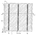
- FIG. 1 is a plan view schematically showing the appearance of a light receiving surface of a solar cell element according to an embodiment of the present invention.
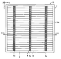
- FIG. 2 is a plan view schematically showing the appearance of the non-light-receiving surface of the solar cell element according to one embodiment of the present invention.
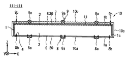
- FIG. 3 is a view showing an XZ cross section at the position indicated by the line III-III in FIGS.
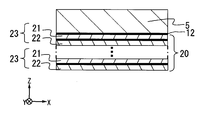
- FIG. 4 is an enlarged cross-sectional view schematically showing the first protective layer in FIG.
- FIG. 5 is an enlarged cross-sectional view schematically showing the second protective layer in FIG.
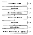
- FIG. 6 is a flowchart showing a manufacturing flow of the solar cell element according to the embodiment of the present invention.
- FIG. 7 is a plan view showing a region where the third semiconductor region is formed.
- FIG. 8 is an exploded view schematically showing a cross section of a solar cell module according to an embodiment of the present invention.
- FIG. 9 is a plan view schematically showing the appearance of a
- FIGS. 7 to 9 show a right-handed XYZ coordinate system in which the direction perpendicular to the extending direction of the first output extraction electrode 8a (the right direction as viewed in FIG. 1) is the + X direction. Is attached.
- FIG. 3 which is a cross-sectional view, only a part is hatched for simplicity.
- the solar cell element 10 has a first main surface 10a, a second main surface 10b, and a side surface 10c.
- the second main surface 10b is a surface (light receiving surface) that mainly receives incident light.
- the first main surface 10a is a surface (for example, a non-light receiving surface) located on the opposite side of the second main surface 10b of the solar cell element 10.
- the side surface 10c is a surface that connects the first main surface 10a and the second main surface 10b.
- the second main surface 10 b is drawn as the upper surface of the solar cell element 10 on the + Z direction side
- the first main surface 10 a is drawn as the lower surface of the solar cell element 10 on the ⁇ Z direction side.
- the solar cell element 10 includes a semiconductor substrate 1, a first passivation layer 5, a second passivation layer 6, an antireflection layer 7, a first electrode 8, and a second electrode 9. Furthermore, the solar cell element 10 has at least a first protective layer 12 on the first passivation layer 5.
- the solar cell element 10 may have a layer functioning as a protective layer in addition to the first protective layer 12 on the first passivation layer 5. For example, as shown in FIG. 4, a first protective layer 12 and a first repeating structure 20 that function as a protective layer are stacked in this order on the first passivation layer 5. For example, as shown in FIG.
- each of the first protective layer 12, the first repeating structure 20, the second protective layer 13, and the second repeating structure 30 has an oxide containing at least one of zirconium (Zr) and hafnium (Hf). is doing.
- the passivation effect of the first passivation layer 5 and the second passivation layer 6 includes a passivation effect (field effect passivation) due to a built-in electric field (an electric field is formed in the vicinity of the interface due to the presence of the passivation layer), and dangling of the interface.
- a passivation effect chemical passivation
- field effect passivation means that the larger the fixed charge density of the passivation layer, the more effective the effect.
- the passivation layer has a higher negative fixed charge density.
- Chemical passivation means that the smaller the interface state density is, the more effective it is.
- the semiconductor substrate 1 has a configuration in which a first semiconductor region 2 that is a p-type semiconductor region and a second semiconductor region 3 that is an n-type semiconductor region are stacked.
- the first semiconductor region 2 is located closest to the first main surface 1a (the surface on the ⁇ Z direction side in the drawing) of the semiconductor substrate 1.
- the second semiconductor region 3 is located closest to the second main surface 1 b (surface on the + Z direction side in the drawing) of the semiconductor substrate 1.
- the first semiconductor region 2 is a p-type conductive semiconductor region
- the second semiconductor region 3 is an n-type conductive semiconductor region.
- the first semiconductor region 2 and the second semiconductor region 3 form a pn junction region.
- the semiconductor substrate 1 includes a semiconductor junction region in which another semiconductor region such as an i-type semiconductor region is interposed between the first semiconductor region 2 and the second semiconductor region 3, for example. May be.
- the semiconductor of the first semiconductor region 2 for example, crystalline silicon (c-Si) such as single crystal silicon and polycrystalline silicon, or amorphous silicon (a-Si) can be employed.
- c-Si crystalline silicon
- a-Si amorphous silicon
- B boron
- Ga gallium
- the thickness of the first semiconductor region 2 is, for example, 250 ⁇ m or less, and may be 150 ⁇ m or less.
- the shape of the first semiconductor region 2 is not particularly limited. For example, if the shape is a quadrangular shape in plan view, the first semiconductor region 2 can be easily manufactured.
- the second semiconductor region 3 is formed by diffusing an element serving as an n-type dopant into a region on the second main surface 1b side of a p-type crystalline silicon substrate (hereinafter referred to as a crystalline silicon substrate). It is formed in the surface layer on the second main surface 1b side in the substrate. At this time, a portion other than the second semiconductor region 3 in the crystalline silicon substrate can be the first semiconductor region 2.
- the n-type dopant may be phosphorus (P), for example.
- an uneven portion 11 is arranged on the second main surface 1 b of the semiconductor substrate 1.
- the height of the convex portion in the concavo-convex portion 11 may be, for example, 0.1 ⁇ m or more and 10 ⁇ m or less, and the width of the convex portion may be, for example, about 1 ⁇ m or more and about 20 ⁇ m or less.
- grooved part 11 should just be a substantially spherical shape, for example.
- the height of the convex portion referred to here is a convex portion from the reference plane in the normal direction of the reference plane with reference to a plane (reference plane) passing through the bottom surface of the concave portion and parallel to the first main surface 10a.
- variety of a convex part here means the distance between the bottom faces of an adjacent recessed part in the direction parallel to the said reference plane.
- the first passivation layer 5 is disposed on the first main surface 1 a side of the semiconductor substrate 1. That is, the first passivation layer 5 is disposed on the first main surface 1 a side of the first semiconductor region 2.
- a material of the first passivation layer 5 for example, aluminum oxide may be employed.
- the first passivation layer 5 is present in the solar cell element 10, minority carrier recombination on the first major surface 1 a of the semiconductor substrate 1 is reduced due to the passivation effect. Thereby, since the open circuit voltage and short circuit current of the solar cell element 10 increase, the output characteristic of the solar cell element 10 improves.
- the average value of the thickness of the 1st passivation layer 5 should just be 3 nm or more and about 100 nm or less, for example.
- a layer functioning as passivation may be further interposed between the first semiconductor region 2 and the first passivation layer 5.
- the first passivation layer is aluminum oxide
- an oxide layer containing silicon such as silicon oxide and functioning as passivation may be interposed between the first semiconductor region 2 and the first passivation layer 5.
- the energy in the direction in which electrons as minority carriers decrease in the vicinity of the interface with the first passivation layer 5 in the first semiconductor region 2.
- the band bends. Specifically, in the first semiconductor region, the energy band is bent so that the closer to the interface with the first passivation layer 5, the closer the electron potential increases. Thereby, the passivation effect by what is called a built-in electric field increases. Further, the composition and the like of the first passivation layer 5 are appropriately adjusted, so that the passivation effect due to the built-in electric field and the passivation effect due to dangling bond termination are increased.
- the second passivation layer 6 is disposed on the second main surface 1b side of the semiconductor substrate 1. That is, the second passivation layer 6 is disposed on the second main surface 1 b side of the second semiconductor region 3.
- the second passivation layer 6 exists, minority carrier recombination on the second main surface 1b side of the semiconductor substrate 1 is reduced by a passivation effect due to the so-called dangling bond termination.
- the average value of the thickness of the 2nd passivation layer 6 should just be 3 nm or more and about 100 nm or less, for example.
- the second passivation layer 6 when aluminum oxide is adopted as the material of the second passivation layer 6, for example, a positive interface fixed charge density or a negative interface fixed charge smaller than the aluminum oxide is formed on the second passivation layer 6.
- the antireflection layer 7 having a density may be disposed. If such a configuration is adopted, the second passivation layer 6 has a negative interface fixed charge density in the vicinity of the interface with the second passivation layer 6 in the second semiconductor region 3, so that holes that are minority carriers are used. The problem that the energy band bends in the direction of increasing is reduced. As a result, characteristic deterioration due to an increase in minority carrier recombination on the second main surface 1b side of the semiconductor substrate 1 is suppressed.
- the first passivation layer 5 and the second passivation layer 6 can be easily formed by using an ALD (Atomic Layer Deposition) method.
- ALD Atomic Layer Deposition
- Al organic metal gas containing aluminum
- TMA trimethylaluminum
- TEA triethylaluminum
- O 3 ozone
- H water
- O oxygen
- O oxygen
- a first protective layer 12 having a thickness of 50 nm or less is disposed on the first passivation layer 5, for example.
- moisture permeability from the outside can be suppressed so that the passivation effect is not impaired, and the electrical characteristics and the like of the solar cell element 10 are not impaired.
- reliability and the like can be improved.
- the first protective layer 12 when the first protective layer 12 is formed by a film forming method, the first protective layer 12 is formed and arranged by an ALD method, a sputtering method, a MOCVD (Metal-Organic-Chemical-Vapor-Deposition) method, a P-CVD (Plasma-Chemical-Vapor Deposition) method, or the like.
- ALD method atomic layer deposition
- MOCVD Metal-Organic-Chemical-Vapor-Deposition
- P-CVD Pasma-Chemical-Vapor Deposition
- this oxide layer is formed on the first passivation layer 5 by, for example, an ALD method, a sputtering method, an MOCVD method, or a P-CVD method, the oxide layer is formed between the oxide layer and the first passivation layer 5.
- One protective layer 12 is naturally formed. In this case, the thickness of the first protective layer 12 is about 1 nm or thinner.
- the first protective layer 12 has an oxide containing at least one of zirconium and hafnium.
- the first protective layer 12 is an oxide containing zirconium, for example, Zr x Al y O 1-xy , Zr x Mg y O 1-xy , Zr x Ca y O 1-xy Or Zr x Y y O 1-xy .
- the first protective layer 12 is an oxide containing hafnium, for example, Hf x Al y O 1-xy , Hf x Mg y O 1-xy , Hf x Ca y O 1-x, -y or Hf x Y y O 1-x -y or the like.
- the above x and y satisfy the relations of 0 ⁇ y ⁇ 1, 0 ⁇ x ⁇ 1, and x + y ⁇ 1.
- These oxides are all excellent in terms of moisture permeability suppression and thermal stability.
- these oxides in particular, when Zr x Al y O 1-xy or Hf x Al y O 1-xy is used, when the first passivation layer 5 is an AlO x film, It is suitable for the reason that it can be easily produced.
- a first oxide layer 21 made of zirconium oxide (for example, ZrO 2 ) or hafnium oxide (for example, HfO 2 ) may be disposed on the first protective layer 12.
- a second oxide layer 22 made of aluminum oxide may be disposed on the first oxide layer 21. That is, the first protection unit layer 23 in which the first oxide layer 21 and the second oxide layer 22 are provided in this order may be arranged from a position close to the first passivation layer 5 to a position far from the first passivation layer 5. For example, as shown in FIG.
- the first oxide layer 21 of the zirconium oxide layer or the hafnium oxide layer and the second oxide layer 22 of the aluminum oxide layer are formed from the side closer to the first passivation layer 5 to the side farther from this side. You may have the 1st protection unit layer 23 laminated
- the first oxide layer 21 and the second oxide layer 22 each have a thickness of, for example, not less than 0.1 nm and not more than 10 nm.
- an oxide layer similar to the first protective layer 12 can be formed at the interface between the two oxide layers (between the first oxide layer 21 and the second oxide layer 22).
- the first oxide layer 21 is made of zirconium oxide
- a composite such as Zr x Al y O 1- xy is interposed between the first oxide layer 21 and the second oxide layer 22.
- the oxide layer can be naturally formed with a thickness of about 1 nm or thinner.
- Hf x Al y O 1-xy or the like is provided between the first oxide layer 21 and the second oxide layer 22.
- These composite oxide layers can be naturally formed with a thickness of about 1 nm or thinner. The presence of such a composite oxide layer is preferable because the presence of the composite oxide layer improves the thermal stability and moisture permeability of the solar cell element 10.
- the first protective unit layer 23 has the first repeating structure 20 in which a plurality of layers are stacked, a plurality of complex oxide layers exist, and the above-described effects are obtained. It will be noticeable.
- an oxide layer containing zirconium and aluminum or hafnium is provided between adjacent first protection unit layers 23.
- an oxide layer comprising aluminum may intervene.
- a composite oxide layer such as Zr x Al y O 1-xy has a thickness between the adjacent first protection unit layers 23. It can be naturally formed as thin as about 1 nm or thinner.
- first oxide layer 21 is made of hafnium oxide
- a composite oxide layer such as Hf x Al y O 1- xy is interposed between the adjacent first protection unit layers 23.
- Hf x Al y O 1- xy is interposed between the adjacent first protection unit layers 23.
- a second protective layer 13 having a composition similar to that of the first protective layer 12 having a thickness of 50 nm or less, for example, may be disposed on the second passivation layer 6.
- This second protective layer 13 also has the same effect as the first protective layer 12.
- the second protective layer 13 is formed by a film forming method
- the second protective layer 13 is formed and disposed by an ALD method, a sputtering method, an MOCVD method, a P-CVD method, or the like.
- the second protective layer 13 may be formed naturally when an oxide layer made of zirconium oxide or hafnium oxide is formed on the second passivation layer 6.
- this oxide layer is formed on the second passivation layer 6 by, for example, an ALD method, a sputtering method, an MOCVD method, or a P-CVD method, the oxide layer is interposed between the oxide layer and the second passivation layer 6. 2
- the protective layer 13 is naturally formed. In this case, the thickness of the second protective layer 13 is about 1 nm or thinner.
- the second protective layer 13 has an oxide containing at least one of zirconium and hafnium.
- the second protective layer 13 is an oxide containing zirconium, for example, Zr x Al y O 1-xy , Zr x Mg y O 1-xy , Zr x Ca y O 1-xy Or Zr x Y y O 1-xy .
- the second protective layer 13 is an oxide containing hafnium, for example, Hf x Al y O 1-xy , Hf x Mg y O 1-xy , Hf x Ca y O 1-x -y or Hf x Y y O 1-x -y or the like.
- the above x and y satisfy the relations of 0 ⁇ y ⁇ 1, 0 ⁇ x ⁇ 1, and x + y ⁇ 1.
- These oxides are all excellent in terms of moisture permeability suppression and thermal stability.
- these oxides in particular, when Zr x Al y O 1-xy or Hf x Al y O 1-xy is used, when the second passivation layer 6 is an AlO x film, It is suitable for the reason that it can be easily produced.
- a third oxide layer 31 made of zirconium oxide or hafnium oxide may be disposed on the second passivation layer 6.
- a fourth oxide layer 32 made of aluminum oxide may be disposed on the third oxide layer 31. That is, the second protection unit layer 33 in which the third oxide layer 31 and the fourth oxide layer 32 are provided in this order may be arranged from a position close to the second passivation layer 6 to a position far from the second passivation layer 6.
- a third oxide layer 31 of a zirconium oxide layer or a hafnium oxide layer and a fourth oxide layer 32 of an aluminum oxide layer are formed from the side closer to the second passivation layer 6 to the side farther from this side. You may have the 1st protection unit layer 33 laminated
- the thicknesses of the third oxide layer 31 and the fourth oxide layer 32 are, for example, not less than 0.1 nm and not more than 10 nm.
- an oxide layer similar to the second protective layer 13 can be formed at the interface between the two oxide layers (between the third oxide layer 31 and the fourth oxide layer 32).
- the third oxide layer 31 is made of zirconium oxide
- a composite oxide layer such as Zr x Al y O 1- xy is interposed between the third oxide layer 31 and the fourth oxide layer 32.
- the third oxide layer 31 is made of hafnium oxide
- there is a gap between the third oxide layer 31 and the fourth oxide layer 32 such as Hf x Al y O 1-xy.
- These composite oxide layers can be naturally formed with a thickness of about 1 nm or thinner. The presence of such a complex oxide layer may further improve the thermal stability and moisture permeability of the solar cell element 10.
- the second protective unit layer 33 when the second protective unit layer 33 includes the second repeated structure 30 in which a plurality of layers are stacked, a plurality of complex oxide layers exist, and thus the above-described effects. Can be prominent.
- an oxide layer containing zirconium and aluminum or hafnium is provided between the adjacent second protective unit layers 33.
- an oxide layer comprising aluminum may intervene.
- the third oxide layer 31 is made of zirconium oxide
- a composite oxide layer such as Zr x Al y O 1-xy has a thickness between the adjacent second protection unit layers 33. It can be naturally formed as thin as about 1 nm or thinner.
- the third oxide layer 31 is made of hafnium oxide
- a composite oxide layer such as Hf x Al y O 1- xy is interposed between the adjacent second protection unit layers 33.
- it can be naturally formed with a thickness of about 1 nm or thinner.
- the first protective layer 12, the first repetitive structure 20, the second protective layer 13 and the second repetitive structure 30 are all the same as the first passivation layer 5 and the second passivation layer 6 in order to maintain the passivation effect. May have a negative fixed charge.
- the antireflection layer 7 is a layer for improving the efficiency of light absorption in the solar cell element 10.
- the antireflection layer 7 is disposed on the second main surface 10 b side of the second passivation layer 6.
- the material of the antireflection layer 7 may be, for example, silicon nitride or silicon oxide.
- the thickness of the antireflection layer 7 may be appropriately set according to the materials of the semiconductor substrate 1 and the antireflection layer 7.
- the antireflection layer 7 is silicon nitride (Si 3 N 4 or the like) or silicon oxide
- the antireflection layer 7 and the fourth oxide layer 32 adjacent to each other are made of an oxide containing aluminum and silicon.
- the three protective layers 14 can be formed naturally with a thickness of about 1 nm or thinner.
- the second protective layer 13 the oxide layer present between the third oxide layer 31 and the fourth oxide layer 32, the oxide layer present between the adjacent second protection unit layers 33, and antireflection
- the presence of the elements constituting the oxide layer existing between the layer 7 and the fourth oxide layer 32 adjacent thereto is, for example, SIMS (Secondary Ion Mass Mass Spectrometry), TEM (Transmission Electron Microscope), EELS (Electron Energy- It can be confirmed by an analytical method such as Loss Spectroscopy), XPS (X-ray Photoelectron Spectroscopy) or RBS (Rutherford Backscattering Spectrometry).
- the solar cell element 10 when the solar cell element 10 has the antireflection layer 7, the solar cell element 10 realizes a condition that is difficult to be reflected with respect to light in a specific wavelength region.
- the light in the specific wavelength region refers to a wavelength region around the peak wavelength of the irradiation intensity of sunlight.
- the refractive index of the antireflection layer 7 may be, for example, about 1.8 or more and 2.3 or less.
- the average value may be, for example, about 20 nm or more and 120 nm or less.
- the antireflection layer 7 may be provided on the side surface 10 c side of the semiconductor substrate 1. In this case, since the antireflection layer 7 becomes dense when it is formed by the ALD method, the formation of minute openings such as pinholes on the side surface 10c of the semiconductor substrate 1 is greatly reduced. Therefore, it is possible to avoid deterioration of characteristics due to generation of leakage current.
- the third semiconductor region 4 is disposed on the first main surface 1a side of the semiconductor substrate 1.
- the third semiconductor region 4 has the same p-type conductivity type as the first semiconductor region 2.
- the dopant concentration in the third semiconductor region 4 is higher than the dopant concentration in the first semiconductor region 2. That is, the third semiconductor region 4 is formed by doping the semiconductor substrate 1 with a p-type dopant at a higher concentration than the p-type dopant doped in the semiconductor substrate 1 to form the first semiconductor region 2. Is done.
- the third semiconductor region 4 has a role of generating a built-in electric field on the first main surface 1 a side of the semiconductor substrate 1 and reducing recombination of minority carriers in the region on the first main surface 1 a side of the semiconductor substrate 1. ing. For this reason, the conversion efficiency in the solar cell element 10 can be further increased by the presence of the third semiconductor region 4.
- the third semiconductor region 4 is formed, for example, by doping an element serving as a dopant such as boron or aluminum on the first main surface 1a side of the semiconductor substrate 1.
- the first electrode 8 is disposed on the first main surface 10 a side of the semiconductor substrate 1. As shown in FIG. 2, the first electrode 8 includes, for example, a plurality of first output extraction electrodes 8a extending in the Y direction, and a large number of linear first current collecting electrodes 8b extending in the X direction. It is included. Here, at least a part of the first output extraction electrode 8a is electrically connected to the plurality of first current collection electrodes 8b by intersecting with the plurality of linear first current collection electrodes 8b.
- the width of the first current collecting electrode 8b in the short direction may be, for example, about 50 ⁇ m or more and about 300 ⁇ m or less.
- variety in the transversal direction of the 1st output extraction electrode 8a should just be 1.3 mm or more and about 3 mm or less, for example. That is, the width in the short direction of the first current collecting electrode 8b may be smaller than the width in the short direction of the first output extraction electrode 8a.
- interval of adjacent 1st current collection electrode 8b among the some 1st current collection electrodes 8b should just be 1.5 mm or more and about 3 mm or less.
- the thickness of the 1st electrode 8 should just be about 10 micrometers or more and about 40 micrometers or less, for example.
- the first electrode 8 is fired after, for example, a conductive paste (silver paste) containing silver as a main component is applied in a desired pattern on the first main surface 1a of the semiconductor substrate 1 by screen printing or the like. Is formed. Further, aluminum may be mainly used as the material of the first current collecting electrode 8b, and silver may be mainly used as the material of the first output extraction electrode 8a.
- a conductive paste silver paste
- the second electrode 9 is disposed on the second main surface 10b side of the semiconductor substrate 1.
- the second electrode 9 includes, for example, a plurality of second output extraction electrodes 9a extending in the Y direction, and a large number of linear second current collecting electrodes 9b extending in the X direction. It is included.
- at least a part of the second output extraction electrode 9a is electrically connected to the plurality of second current collection electrodes 9b by intersecting with the plurality of linear second current collection electrodes 9b.
- the width of the second current collecting electrode 9b in the short direction may be, for example, about 50 ⁇ m or more and about 200 ⁇ m or less.
- variety in the transversal direction of the 2nd output extraction electrode 9a should just be 1.3 mm or more and about 2.5 mm or less, for example. That is, the width of the second collector electrode 9b in the short direction may be smaller than the width of the second output extraction electrode 9a in the short direction.
- interval of the adjacent 2nd current collection electrodes 9b among the some 2nd current collection electrodes 9b should just be 1.5 mm or more and about 3 mm or less.
- the thickness of the 2nd electrode 9 should just be about 10 micrometers or more and about 40 micrometers or less, for example.
- the 2nd electrode 9 is formed by baking after apply
- aluminum oxide is a stoichiometric composition of Al 2 O 3 in which the ratio of the atomic density of aluminum (Al) (first ratio) R Al / O is 2/3 based on the atomic density of oxygen (O).
- the atomic density means the number of atoms per unit volume, and is represented by, for example, the number of atoms per 1 cm 3 (unit is atoms / cm 3 ).
- the first ratio R Al / O is less than 2/3, specifically, the first ratio obtained by dividing the atomic density of aluminum by the atomic density of oxygen is less than 0.667, Al is deficient. There can be parts.
- the aluminum oxide that is the passivation layer of this embodiment is considered to generate a negative fixed charge density due to the compositional defect of Al.
- the aluminum oxide has a non-stoichiometric composition and is presumed to have an amorphous structure close to ⁇ -alumina. This has been confirmed by TEM or EELS.
- the negative fixed charge density can be increased when there are more Al compositional defects.
- the lower limit of the Al compositional deficiency is a non-stoichiometric aluminum oxide having a composition of about Al 1.9 O 3.1 .
- the first ratio R Al / O is about 0.613 ( ⁇ 1.9 / 3.1). Therefore, if the first ratio R Al / O is not less than 0.613 and less than 0.667, the aluminum oxide can have a large negative fixed charge density.
- the aluminum oxide contains hydrogen (H), CH n (n is a natural number), etc.
- silicon (Si) in the first semiconductor region 2 is formed at the interface between the first passivation layer 5 and the first semiconductor region 2.
- Dangling bonds are terminated by H, OH, CH n (n is a natural number), O or the like. That is, the effect of passivation is increased by reducing the interface state density.
- the fixed charge Q in the Al deficient portion decreases from ⁇ 3 to ⁇ 2 valence, but it is presumed that the instability in the Al deficient portion is alleviated by the OH bond. Therefore, the stability of non-stoichiometric aluminum oxide having Al deficiency can be increased. As a result, for example, even if heat treatment is performed when the antireflection layer 7, the first electrode 8, and the second electrode 9 are formed after the first passivation layer 5 is formed, Al deficient portions in the aluminum oxide are formed. Can be difficult to disappear.
- the ratio (second ratio) R (Al + H) / O of the sum of the atomic density of Al and the atomic density of H based on the atomic density of O is 2/3 or more, specifically If it is 0.667 or more, the stability of the Al deficient portion can be enhanced.
- the negative fixed charge generation mechanism on the aluminum oxide side is considered as follows, for example.
- another secondary reaction continues.
- the positive charge generated on the Si side acts to bend the Si band upward toward the interface. That is, a potential barrier is generated for an electron which is a minority carrier existing in the conduction band, and it is suppressed that the electron flows into the interface, recombines and disappears. That is, the effect of increasing the effective lifetime of minority carriers is exhibited (field effect passivation).
- the negative charges generated on the aluminum oxide side are fixed in the aluminum oxide near the interface. That is, it becomes a negative fixed charge. Since the negative fixed charge in the aluminum oxide is extremely stable, it is not lost even during the manufacturing process of the solar cell element (during a high-temperature process such as firing). That is, the stable existence of negative fixed charges ensures the stability of positive charges on the Si side (stability of field effect passivation).
- the energy band is bent so that the closer to the interface with the first passivation layer 5, the higher the energy of electrons.
- the passivation effect by what is called a built-in electric field can increase.
- the composition of the first passivation layer 5 is appropriately adjusted, so that the passivation effect due to the built-in electric field can be further increased.
- the second ratio R (Al + H) / O is a value obtained by dividing the sum of the atomic density of Al and the atomic density of H by the atomic density of O.
- the upper limit of the H content is up to a composition of about (Al + H) 2.2 O 2.8 as non-stoichiometric aluminum oxide.
- the second ratio R (Al + H) / O is about 0.786 ( ⁇ 2.2 / 2.8). Therefore, if the second ratio R (Al + H) / O is 0.667 or more and less than 0.786, the stability of the Al deficient portion in the non-stoichiometric aluminum oxide can be increased. That is, the passivation effect by aluminum oxide can occur stably.
- the first ratio R Al / O is 0.613 or more and less than 0.667
- the second ratio R (Al + H) / O is 0.667 or more.
- the passivation effect by aluminum oxide may arise stably.
- the effective lifetime required for recombination of minority carriers in the first semiconductor region 2 can be extended. That is, the conversion efficiency in the solar cell element 10 can be further increased by improving the passivation effect.
- the inside of the first passivation layer 5 may be, for example, an inner portion excluding the vicinity of both main surfaces in the thickness direction of the first passivation layer 5. That is, the inside of the first passivation layer 5 does not include the vicinity of the interface with the first semiconductor region 2 in the first passivation layer 5. Further, the inside of the first passivation layer 5 may be a central portion in the thickness direction of the first passivation layer 5.
- the vicinity of the interface between the first passivation layer 5 and the first semiconductor region 2 is, for example, about 3 nm or more and 10 nm or less in the first passivation layer 5 from the interface between the first passivation layer 5 and the first semiconductor region 2. Any area corresponding to the thickness of the film may be used. If the thickness of the first passivation layer 5 is 10 nm or less, almost the entire thickness may be regarded as near the interface.
- the first ratio R Al / O in the vicinity of the interface with the first semiconductor region 2 in the first passivation layer 5 is larger than the first ratio R Al / O in the central portion in the thickness direction of the first passivation layer 5.
- the passivation effect due to the built-in electric field and the passivation effect due to the termination of dangling bonds in the Si at the interface can be improved. That is, the effective lifetime in the first semiconductor region 2 can be extended, and the conversion efficiency in the solar cell element 10 can be further increased.
- the passivation effect can be improved.
- the sum (total atomic density) A H + C of the atomic density A H of H and the atomic density AC of C in the vicinity of the interface with the first semiconductor region 2 in the first passivation layer 5 is the first passivation layer. 5 should be larger than the total atomic density A H + C at the center in the thickness direction.
- the dangling bond of Si as the semiconductor material of the first semiconductor region 2 only needs to be terminated by a methyl group at the interface between the first passivation layer 5 and the first semiconductor region 2.
- the effect of the passivation by the first passivation layer 5 is further increased.
- the effective lifetime in the first semiconductor region 2 is extended, and the conversion efficiency in the solar cell element 10 is further increased.
- the atomic density A H of H and the atomic density AC of C are effective in the first semiconductor region 2. Lifetime is extended.
- the ratio of the atomic density of H based on the atomic density of C in the vicinity of the interface with the first semiconductor region 2 in the first passivation layer 5 (value obtained by dividing the atomic density of H by the atomic density of C: 3 ratio) R H / C only needs to be larger than the third ratio R H / C in the center portion in the thickness direction of the first passivation layer 5. In this case, since the passivation effect can be improved, the effective lifetime in the first semiconductor region 2 is extended, and the conversion efficiency in the solar cell element 10 is further increased.
- the third ratio R H / C is more than 1 near the interface with the first semiconductor region 2 in the first passivation layer 5. growing. For this reason, it is estimated that H exists mainly in the form of H (or OH) or CH n (n is a natural number) in the vicinity of the interface with the first semiconductor region 2 in the first passivation layer 5. On the other hand, the third ratio RH / C is less than 1 in the region from the central portion in the thickness direction of the first passivation layer 5 to the first main surface 10a.
- H exists mainly in the form of H (or OH), and C is mainly bonded to Al or O. It is presumed to exist in the form.
- the dangling bond of Si as the semiconductor material of the first semiconductor region 2 is terminated by a methyl group or the like at the interface between the first passivation layer 5 and the first semiconductor region 2. Is done. With such a structure, the effect of passivation by the first passivation layer 5 is further increased. As a result, the effective lifetime in the first semiconductor region 2 is extended, and the conversion efficiency in the solar cell element 10 is further increased.
- FIG. 6 is a flowchart illustrating the manufacturing flow of the solar cell element 10.
- the solar cell element 10 is manufactured by performing step SP1 to step SP7 in order.
- step SP1 a process of preparing a p-type semiconductor substrate 1 is performed.
- the semiconductor substrate 1 is a single crystal silicon substrate
- the semiconductor substrate 1 is formed using, for example, an FZ (Floating Zone) method or the like.
- the semiconductor substrate 1 is a polycrystalline silicon substrate
- the semiconductor substrate 1 is formed using a casting method etc., for example.
- a p-type polycrystalline silicon substrate is used as the semiconductor substrate 1 will be described.
- an ingot of polycrystalline silicon as a semiconductor material is produced by a casting method.
- the ingot is sliced into a thickness of, for example, 250 ⁇ m or less.
- the surface of the semiconductor substrate 1 is mechanically damaged at the cut surface of the semiconductor substrate 1 by performing a very small amount of etching using an aqueous solution of NaOH, KOH, hydrofluoric acid, or hydrofluoric nitric acid. Remove layer and contaminated layer.
- an uneven portion is formed on at least the second main surface 1b of the first and second main surfaces 1a and 1b of the semiconductor substrate 1.
- a method for forming the uneven portion for example, a wet etching method using an alkaline solution such as NaOH or an acid solution such as hydrofluoric acid, or a dry etching method using RIE (ReactiveRIIon Etching) or the like is employed.
- an n-type conductive second semiconductor region 3 is formed on the second main surface 1b of the semiconductor substrate 1 on which the concavo-convex portion is formed.
- the thickness of the second semiconductor region 3 may be about 0.2 ⁇ m or more and about 2 ⁇ m or less.
- the sheet resistance value of the second semiconductor region 3 may be about 40 ⁇ / ⁇ or more and about 200 ⁇ / ⁇ or less.
- a coating thermal diffusion method in which thermal diffusion is performed after applying paste-like P 2 O 5 to the surface of the semiconductor substrate 1, or POCl 3 (oxy) in a gas state is used.
- a vapor phase thermal diffusion method using phosphorus chloride) as a diffusion source is employed.
- the vapor phase thermal diffusion method when the vapor phase thermal diffusion method is adopted, first, heat treatment is performed on the semiconductor substrate 1 in a temperature range of about 600 ° C. and about 800 ° C. in an atmosphere containing a diffusion gas such as POCl 3. Is given. Thereby, phosphorous glass is formed on the second main surface 1b of the semiconductor substrate 1.
- the heat treatment time may be, for example, about 5 minutes or more and within about 30 minutes.
- heat treatment is performed on the semiconductor substrate 1 in a high temperature range of about 800 ° C. to 900 ° C. in an atmosphere mainly containing an inert gas such as argon and nitrogen.
- the heat treatment time may be, for example, about 10 minutes or more and about 40 minutes or less.
- the second semiconductor region 3 is formed on the first main surface 1a side of the semiconductor substrate 1 when the second semiconductor region 3 is formed, the second semiconductor region 3 is formed on the first main surface 1a side.
- the semiconductor region 3 may be removed by etching.
- the p-type conductive semiconductor region 2 is exposed on the first main surface 1 a of the semiconductor substrate 1.
- the second semiconductor region 3 formed on the first main surface 1a side is removed by immersing only the first main surface 1a side of the semiconductor substrate 1 in a hydrofluoric acid solution. Thereafter, the phosphor glass formed on the second main surface 1b side of the semiconductor substrate 1 may be removed by etching.
- the second main surface 1b side is removed by removing the second semiconductor region 3 formed on the first main surface 1a side in the state where the phosphor glass remains on the second main surface 1b of the semiconductor substrate 1.
- the removal of the second semiconductor region 3 and the damage given to the second semiconductor region 3 are unlikely to occur.
- the second semiconductor region 3 formed on the side surface 1c of the semiconductor substrate 1 with the phosphor glass remaining on the second main surface 1b of the semiconductor substrate 1 may be removed together.
- the second semiconductor region 3 may be formed by vapor phase thermal diffusion or the like in a state where the diffusion mask is previously arranged on the first main surface 1a of the semiconductor substrate 1, and then the diffusion mask may be removed. . According to such a process, the second semiconductor region 3 is not formed on the first main surface 1 a side of the semiconductor substrate 1. For this reason, the process of removing the 2nd semiconductor region 3 formed in the 1st main surface 1a side of the semiconductor substrate 1 becomes unnecessary.
- the method of forming the second semiconductor region 3 is not limited to the above method.
- an n-type hydrogenated amorphous silicon film or a crystalline silicon film including a microcrystalline silicon film may be formed using thin film technology.
- a silicon region having i-type conductivity may be formed between the first semiconductor region 2 and the second semiconductor region 3.
- the first passivation layer 5 is formed on the first main surface 1a of the first semiconductor region 2, and the second passivation layer 6 is formed on the second main surface 1b of the second semiconductor region 3.
- a method for forming the first passivation layer 5 and the second passivation layer 6 for example, an ALD method can be employed. Thereby, the first passivation layer 5 and the second passivation layer 6 can be formed simultaneously around the entire periphery of the semiconductor substrate 1. That is, a passivation layer including an aluminum oxide layer can be formed also on the side surface 1 c of the semiconductor substrate 1.
- the semiconductor substrate 1 on which the second semiconductor region 3 is formed in step SP3 is placed in the chamber of the film forming apparatus, and the semiconductor substrate 1 is at 100 ° C. or higher and 250 ° C. In the state heated in the following temperature range, the following process A to process D are repeated. Thereby, the 1st passivation layer 5 and the 2nd passivation layer 6 which have desired thickness are formed.
- Step A By supplying an Al material such as TMA onto the semiconductor substrate 1 together with a carrier gas such as Ar gas or N 2 gas, the Al material is adsorbed around the entire circumference of the semiconductor substrate 1.
- the dangling bonds on the surface of the semiconductor substrate 1 are preferably terminated in the form of OH groups. That is, in the case of the Si substrate, the Si—O—H form is desirable.
- This structure can be formed by pure water rinsing conditions in the step of treating the Si substrate with dilute hydrofluoric acid, subsequent treatment with an oxidizing solution such as nitric acid, or ozone treatment.
- the time for which TMA is supplied may be about 15 milliseconds or more and about 3 seconds or less, for example.
- step A the following reaction occurs. Si—O—H + Al (CH 3 ) 3 ⁇ Si—O—Al (CH 3 ) 2 + CH 4 ⁇
- the Al raw material is adsorbed on the entire periphery of the semiconductor substrate 1.
- Step B By purifying the chamber of the film forming apparatus with N 2 gas, the Al material in the chamber is removed, and among the Al materials physically and chemically adsorbed on the semiconductor substrate 1, the atomic layer level The Al raw material other than the components chemically adsorbed in the step is removed.
- the time for purging the inside of the chamber with N 2 gas may be, for example, about 1 second or more and about several tens of seconds or less.
- Step C By supplying an oxidizing agent such as water or O 3 gas into the chamber of the film forming apparatus, the methyl group as an alkyl group contained in TMA is removed and replaced with an OH group. That is, the following reaction occurs. Si—O—Al—CH 3 + HOH ⁇ Si—O—Al—OH + CH 4 ⁇
- Si—O—Al—CH 3 on the left side should be expressed accurately as “Si—O—Al (CH 3 ) 2 ”, but the notation is complicated, so CH 3
- the above reaction formula expressing only one reaction is shown.
- the time during which the oxidizing agent is supplied into the chamber is preferably not less than 750 milliseconds and not more than 1.1 seconds. Further, for example, when H is supplied together with the oxidizing agent in the chamber, H is more easily contained in the aluminum oxide.
- Step D By purifying the inside of the chamber of the film forming apparatus with N 2 gas, the oxidizing agent in the chamber is removed. At this time, for example, the oxidizing agent that did not contribute to the reaction at the time of forming atomic layer level aluminum oxide on the semiconductor substrate 1 is removed. In addition, the time for which the inside of the chamber is purified by N 2 gas may be about 1 second, for example.
- an aluminum oxide layer having a desired film thickness is formed by repeating a series of steps A to D a plurality of times such as step B ⁇ step C ⁇ step D ⁇ step A ⁇ .
- the first passivation layer 5 and the second passivation layer 6 by the ALD method, even if there are minute irregularities on the surface of the semiconductor substrate 1, an aluminum oxide layer is uniformly formed along the irregularities. Can be done. Thereby, the passivation effect on the surface of the semiconductor substrate 1 can be enhanced.
- step SP5 an example of a manufacturing method of the first protective layer 12 and the first repetitive structure 20 shown in FIG. 4 and the second protective layer 13 and the second repetitive structure 30 shown in FIG. 5 in step SP5 will be described.
- the first protection unit layer 23 and the second protection unit layer 33 are first formed with a first oxide layer 21 and a third oxide layer 31 made of, for example, a zirconium oxide layer or a hafnium oxide layer, and then, for example, an aluminum oxide layer A second oxide layer 22 and a fourth oxide layer 32 made of are formed.
- the first oxide layer 21 and the third oxide layer 31 may be formed by the same method using zirconium or hafnium in place of aluminum in step SP4 described above.
- the reaction occurring in the above steps A and C is the same in zirconium oxide or hafnium oxide.
- the raw material of Zr is TEMAZ (chemical formula: Zr [N (CH 3 ) CH 2 CH 3 ] 4 ) or TDMAZ (chemical formula : [Zr (N (CH 3 ) 2 ) 4 ] 2 ) may be used.
- the reaction formula of the above step A in the case of TEMAZ is Si—O—H + Zr [N (CH 3 ) CH 2 CH 3 ] 4 ⁇ Si—O—Zr [N (CH 3 ) CH 2 CH 3 ] 3 + CH 4 ⁇ + H 2 ⁇ ... .
- TEMAH chemical formula: Hf [N (CH 3 ) CH 2 CH 3 ] 4
- TDMAH chemical formula: [Hf (N (CH 3 ) 2 ) 4 ] 2
- the reaction formula of the above step A is Si—O—H + Hf [N (CH 3 ) CH 2 CH 3 ] 4 ⁇ Si—O—Hf [N (CH 3 ) CH 2 CH 3 ] 3 + CH 4 ⁇ + H 2 ⁇ ... .
- the second oxide layer 22 and the fourth oxide layer 32 can be formed by the same method as in step SP4 described above.
- the first repetitive structure 20 in which a plurality of first protection unit layers 23 are laminated can be formed on the first passivation layer 5, and the second passivation layer 6 can be formed on the second passivation layer 6.
- the second repetitive structure 30 in which a plurality of second protection unit layers 33 are stacked can be formed.
- the first protective layer 12 shown in FIG. 4 is naturally formed when the first oxide layer 21 of the first protective unit layer 23 is formed, and the second protective layer 13 shown in FIG. It can be naturally formed when the third oxide layer 31 of the protection unit layer 33 is formed.
- an oxide layer can be naturally formed between the first oxide layer 21 and the second oxide layer 22 when the second oxide layer 22 is formed.
- an oxide layer can be naturally formed between the adjacent first protection unit layers 23 when the first oxide layer 21 is formed.
- an oxide layer can be naturally formed between the third oxide layer 31 and the fourth oxide layer 32 when the fourth oxide layer 32 is formed.
- an oxide layer can be naturally formed between the adjacent second protection unit layers 33 when the third oxide layer 31 is formed.
- the antireflection layer 7 is formed on the second passivation layer 6 disposed on the second main surface 1b of the semiconductor substrate 1.
- a method for forming the antireflection layer 7 for example, a PECVD (plasma enhanced chemical vapor deposition) method, an ALD method, a vapor deposition method or a sputtering method can be employed.
- a PECVD method plasma enhanced chemical vapor deposition
- an ALD method a vapor deposition method or a sputtering method
- a mixed gas of SiH 4 gas and NH 3 gas is diluted with N 2 gas and converted into plasma by glow discharge decomposition in the chamber. Silicon nitride is deposited on the two-passivation layer 6. Thereby, the antireflection layer 7 containing silicon nitride can be formed.
- the third protective layer 14 shown in FIG. 5 can be naturally formed when the antireflection layer 7 is formed.
- the temperature in the chamber when silicon nitride is deposited may be about 500 ° C., for example.
- the antireflection layer 7 is formed by a PECVD method other than the ALD method, a vapor deposition method, a sputtering method, or the like, whereby the antireflection layer 7 having a desired thickness is formed in a short time. Thereby, the productivity of the solar cell element 10 is improved.
- step SP7 the third semiconductor region 4, the first electrode 8, and the second electrode 9 are formed.
- an aluminum paste containing glass frit and aluminum particles is applied to a predetermined region on the first passivation layer 5.
- the component of the aluminum paste is transmitted through the first passivation layer 5 by the fire-through method in which the heat treatment is performed in a high temperature range of 600 ° C. or higher and 800 ° C. or lower, and the first main layer of the semiconductor substrate 1 is transmitted.
- a third semiconductor region 4 is formed on the surface 1a side.
- an aluminum layer is formed on the first main surface 1 a of the third semiconductor region 4.
- the aluminum layer can be used as the first current collecting electrode 8 b as a part of the first electrode 8.
- the region where the third semiconductor region 4 is formed is, for example, one of the first current collecting electrode 8b and the first output extraction electrode 8a on the first main surface 1a of the semiconductor substrate 1, as shown in FIG. Any region along the broken line 80 where the portion is formed may be used.
- the 1st output extraction electrode 8a is produced using the silver paste containing the metal powder, organic vehicle, and glass frit mainly containing silver (Ag) etc., for example.
- a silver paste is applied on the first passivation layer 5.
- the 1st output extraction electrode 8a is formed by baking a silver paste.
- the maximum temperature in baking should just be 600 degreeC or more and 800 degrees C or less, for example.
- the time for performing the firing for example, the temperature is raised toward the peak temperature, and the temperature is lowered after being held for a certain time near the peak temperature, but may be within a few seconds near the peak temperature.
- a method for applying the silver paste for example, a screen printing method or the like may be employed. After applying the silver paste, the solvent in the silver paste may be evaporated by drying the silver paste at a predetermined temperature.
- the 1st output extraction electrode 8a is electrically connected with the 1st current collection electrode 8b by contacting with the layer of aluminum.
- the 1st output extraction electrode 8a after forming the 1st output extraction electrode 8a, you may form the 1st current collection electrode 8b. Further, the first output extraction electrode 8 a may not be in direct contact with the semiconductor substrate 1, and the first passivation layer 5 may exist between the first output extraction electrode 8 a and the semiconductor substrate 1. The aluminum layer formed on the third semiconductor region 4 may be removed. Moreover, you may form the 1st output extraction electrode 8a and the 1st current collection electrode 8b using the same silver paste.
- the second electrode 9 is produced using, for example, a silver paste containing a metal powder mainly containing Ag or the like, an organic vehicle, and glass frit. Specifically, a silver paste is applied on the second passivation layer 6 of the semiconductor substrate 1. Then, the 2nd electrode 9 is formed by baking a silver paste.
- the maximum temperature in baking should just be 600 degreeC or more and 800 degrees C or less, for example.
- the firing time may be, for example, within a few seconds at the firing peak temperature.
- a method for applying the silver paste for example, a screen printing method or the like may be employed.
- the second electrode 9 includes a second output extraction electrode 9a and a second current collection electrode 9b.
- the second output extraction electrode 9a and the second current collection electrode 9b are used. Can be formed at the same time in one step.
- the first electrode 8 and the second electrode 9 are formed by printing and baking.
- the present invention is not limited to this.
- the first electrode 8 and the second electrode 9 may be formed by other thin film forming methods such as an evaporation method or a sputtering method, or a plating method.
- the effect of passivation by the first passivation layer 5 and the second passivation layer 6 is achieved by setting the maximum temperature of the heat treatment in each step to 800 ° C. or less. Can increase.
- the time for performing the heat treatment in the temperature range of 300 ° C. or more and 500 ° C. or less is, for example, 3 minutes or more and 30 minutes. If it is within.
- the solar cell module 100 includes one or more solar cell elements 10.
- the solar cell module 100 only needs to include a plurality of solar cell elements 10 that are electrically connected.
- Such a solar cell module 100 is formed by connecting a plurality of solar cell elements 10 in series and in parallel, for example, when the electric output of a single solar cell element 10 is small. For example, a practical electric output is taken out by combining a plurality of solar cell modules 100.
- the solar cell module 100 includes a plurality of solar cell elements 10 will be described.
- the solar cell module 100 includes, for example, a laminate in which a transparent member 104, a front side filler 102, a plurality of solar cell elements 10, a wiring member 101, a back side filler 103, and a back surface protective material 105 are laminated.
- the transparent member 104 is a member for protecting the light receiving surface that receives sunlight in the solar cell module 100.
- the transparent member 104 may be a transparent flat plate member, for example.
- As a material of the transparent member 104 for example, glass or the like is employed.
- the front side filler 102 and the back side filler 103 may be, for example, a transparent filler.
- the back surface protective material 105 is a member for protecting the solar cell module 100 from the back surface.
- a material of the back surface protective material 105 for example, polyethylene terephthalate (PET) or polyvinyl fluoride resin (PVF) is adopted.
- PET polyethylene terephthalate
- PVF polyvinyl fluoride resin
- the back surface protective material 105 may have a single layer structure or a laminated structure.
- the wiring member 101 is a member (connecting member) that electrically connects the plurality of solar cell elements 10.
- the solar cell elements 10 adjacent to each other in the Y direction are the first electrode 8 of one solar cell element 10 and the second electrode of the other solar cell element 10. 9 is connected by a wiring member 101.
- the thickness of the wiring member 101 may be, for example, about 0.1 mm or more and about 0.2 mm or less.
- the width of the wiring member 101 may be about 2 mm, for example.
- As the wiring member 101 for example, a member in which the entire surface of a copper foil is coated with solder is used.
- one end of the electrode of the first solar cell element 10 and one end of the electrode of the last solar cell element 10 are respectively connected to the output extraction wiring 106. It is electrically connected to a terminal box 107 as an output extraction part.
- the solar cell module 100 may be provided with the frame 108 which hold
- a material of the frame 108 for example, aluminum having both corrosion resistance and strength is employed.
- EVA EVA
- the material of the front side filler 102 since EVA contains vinyl acetate, it causes hydrolysis over time due to permeation of moisture or water at a high temperature to generate acetic acid. There is a case.
- the damage given to the solar cell element 10 by acetic acid can be reduced by providing the antireflection layer 7 on the second passivation layer 6. As a result, the reliability of the solar cell module 100 can be ensured over a long period of time.
- an acid acceptor containing magnesium hydroxide or calcium hydroxide may be added to this EVA.
- production of the acetic acid from EVA is reduced, durability of the solar cell module 100 improves, and the damage given to the 1st passivation layer 5 and the 2nd passivation layer 6 by an acetic acid is further reduced. As a result, the reliability of the solar cell module 100 is ensured over a long period of time.
- the first passivation layer 5 is disposed on the non-light-receiving surface side of the solar cell element 10, but the present invention is not limited to this.
- the semiconductor substrate 1 when an n-type semiconductor region is disposed on the non-light-receiving surface side and a p-type semiconductor region is disposed on the light-receiving surface side, the first is formed on the light-receiving surface side of the solar cell element 10.
- the passivation layer 5 may be disposed.
- the solar cell element 10 may be, for example, a back contact type solar cell element having a metal wrap through structure in which the second output extraction electrode 9a is disposed on the first main surface 10a side.
- the first passivation layer 5 and the second passivation layer 6 are produced, not only the ALD method but also the CVD method can be applied.
- the first passivation layer 5, the second passivation layer 6, the first protective layer 12, the second protective layer 13, the first repeating structure 20, and the second repeating structure 30 are all manufactured by using the ALD method, thereby providing a process. Can be simplified, and the solar cell element 10 can be rapidly produced.
- ⁇ Preparation of sample> As the semiconductor substrate 1, a large number of polycrystalline silicon substrates each having a square side of about 156 mm and a thickness of about 200 ⁇ m in plan view were prepared. These polycrystalline silicon substrates were doped with boron, and p-type polycrystalline silicon substrates (silicon substrates) having a specific resistance of about 1.5 ⁇ ⁇ cm were used. The surfaces of these silicon substrates were etched with an aqueous NaOH solution, and then washed. The following processing was performed on each silicon substrate thus prepared.
- a texture (uneven structure) was formed on the surface side of the silicon substrate by using the RIE method.
- phosphorus is diffused by a vapor phase thermal diffusion method using phosphorus oxychloride (POCl 3 ) as a diffusion source on a silicon substrate to form an n-type reverse conductivity type layer having a sheet resistance of about 90 ⁇ / ⁇ . Formed on the surface of the substrate.
- the reverse conductivity type layers formed on the side surface and the back surface side of the silicon substrate were removed with a hydrofluoric acid solution, and then the remaining phosphorus glass was removed with a hydrofluoric acid solution.
- a first passivation layer 5 and a second passivation layer 6 made of an aluminum oxide layer were formed on the entire surface of the silicon substrate by ALD.
- a first repetitive structure 20 was formed on the first passivation layer 5, and a second repetitive structure 30 was formed on the second passivation layer 6.
- a silicon substrate was placed in the chamber of the film forming apparatus, and the surface temperature of the silicon substrate was maintained at 100 ° C. to 200 ° C. Then, by repeating Step A to Step D described above, the first passivation layer 5 and the second passivation layer 6 having the desired thickness, and the first repeating structure 20 and the second repeating structure 30 were formed.
- step A of the ALD method N 2 gas was used as a carrier gas.
- the flow rate of the N 2 gas introduced into the chamber was set to about 100 sccm.
- the time (opening time) for supplying TMA into the chamber was about 1 second.
- step B of the ALD method the time from the end of the supply of TMA into the chamber to the start of step C (replacement time) was defined as the time during which the inside of the chamber was cleaned.
- the replacement time was about 15 seconds.
- the flow rate of the N 2 gas introduced into the chamber was about 100 sccm.
- step C of the ALD method O 3 gas was used as an oxidizing agent. Further, the time (opening time) during which the O 3 gas was supplied into the chamber was about 750 milliseconds.
- step A of the ALD method the time from the end of the supply of O 3 gas into the chamber to the start of the next step (replacement time) was defined as the time during which the inside of the chamber was cleaned.
- the replacement time was 15 seconds.
- the flow rate of the N 2 gas introduced into the chamber was set to about 100 sccm.
- the average thickness of the first passivation layer 5 and the second passivation layer 6 was about 30 nm. This average thickness is an average value of the results of measurement at five locations on each of the first passivation layer 5 and the second passivation layer 6 using an ellipsometer (SE-400adv manufactured by SENTECH).
- the silicon substrate in N 2 gas was annealed at about 450 ° C. for 15 minutes.
- the first repetitive structure 20 (a layer in which one or a plurality of first protection unit layers 23 including a first oxide 21 of a zirconium oxide layer and a second oxide layer 22 of an aluminum oxide layer are stacked) and a second The protective layer 30 (a layer in which one or a plurality of second protective unit layers 33 each including a second oxide layer 31 of a zirconium oxide layer and a fourth oxide layer 32 of an aluminum oxide layer are stacked) is formed by the following steps.
- the first oxide layers 21 and 31 were formed, and the second oxide layers 22 and 32 were formed in the same manner as the passivation layer.
- step A of the ALD method N 2 gas was employed as a carrier gas.
- the flow rate of the N 2 gas introduced into the chamber was set to about 100 sccm.
- the time (opening time) for supplying TEMAZ into the chamber was about 2 seconds.
- step B of the ALD method the time from the end of the supply of TEMAZ into the chamber to the start of step C (replacement time) was defined as the time during which the inside of the chamber was cleaned.
- the replacement time was about 40 seconds.
- the flow rate of the N 2 gas introduced into the chamber was set to about 100 sccm.
- step C of the ALD method O 3 gas was used as an oxidizing agent. Further, the time (opening time) during which the O 3 gas was supplied into the chamber was set to about 750 msec.
- step A of the ALD method the time from the end of the supply of O 3 gas into the chamber to the start of the next step (replacement time) was defined as the time during which the chamber was cleaned.
- the replacement time was about 15 seconds.
- the flow rate of the N 2 gas introduced into the chamber was set to about 100 sccm.
- the average thickness of the first oxide layer 21, the third oxide layer 31, the second oxide layer 22, and the fourth oxide layer 32 is set to 1.25 nm, and the first protection unit layer 23 and the second protection layer
- the number of unit layers 33 stacked was as shown in Table 1 (Samples 2 to 4). These average thicknesses were set according to the film formation rate measured and calculated from a zirconium oxide single layer or an aluminum oxide single layer using an ellipsometer (SE-400adv manufactured by SENTECH) in the same manner as described above.
- the first protective layer 12 the oxide layer present between the first oxide layer 21 and the second oxide layer 22, and It was confirmed that the oxide layer existing between the adjacent first protection unit layers 23 was naturally formed.
- the second protective layer 13 the oxide layer present between the third oxide layer 31 and the fourth oxide layer 32, and between the adjacent second protection unit layers 33. It was confirmed that the oxide layer present and the oxide layer present between the antireflection layer 7 and the adjacent fourth oxide layer 32 were naturally formed.
- the presence of elements constituting these oxide layers was confirmed by TEM (TITAN80-300 (manufactured by FET)).
- the first protective layer 12, the oxide layer present between the first oxide layer 21 and the second oxide layer 22, and the oxide layer present between the adjacent first protective unit layers 23 are It was confirmed that the thicknesses were Zr x Al y O 1- xy , each of which was thinner than 1 nm.
- the second protective layer 13, the oxide layer existing between the third oxide layer 31 and the fourth oxide layer 32, and the oxide layer existing between the adjacent second protection unit layers 33 are It was confirmed that the thicknesses were Zr x Al y O 1- xy , each of which was thinner than 1 nm.
- solar cell modules (samples 1 to 4 in Table 1) as shown in FIG. 6 were produced, and the reliability tests shown below were performed on the samples 1 to 4.
- the sample 1 without the first protection unit layer 23 and the second protection unit layer 33 has a low initial Voc retention rate, whereas the samples 2 to 4 have the first protection unit.
- the increase in the number of layers 23 and the second protection unit layer 33 increased the initial Voc retention rate.
- the initial Voc retention rate is 100%. That is, according to this example, it was possible to confirm the effects of the first repeating structure 20 and the second repeating structure 30.
Landscapes
- Photovoltaic Devices (AREA)
- Engineering & Computer Science (AREA)
- Life Sciences & Earth Sciences (AREA)
- Sustainable Development (AREA)
- Microelectronics & Electronic Packaging (AREA)
- Sustainable Energy (AREA)
- Chemical & Material Sciences (AREA)
- Crystallography & Structural Chemistry (AREA)
Abstract
Description
図1から図3に示すように、太陽電池素子10は、第1主面10a、第2主面10bおよび側面10cを有している。第2主面10bは、主に入射光を受光する面(受光面)である。また、第1主面10aは、太陽電池素子10の第2主面10bの反対側に位置する面(例えば非受光面)である。側面10cは、第1主面10aと第2主面10bとを接続する面である。図3では、第2主面10bが太陽電池素子10の+Z方向側の上面として描かれており、第1主面10aが太陽電池素子10の-Z方向側の下面として描かれている。
通常、酸化アルミニウムは、酸素(O)の原子密度を基準としたアルミニウム(Al)の原子密度の比率(第1比率)RAl/Oが2/3であるAl2O3の化学量論組成を有する。ここで、原子密度は、単位体積当たりの原子数を意味し、例えば、1cm3当たりの原子数(単位がatoms/cm3)で示される。しかし、第1比率RAl/Oが、2/3未満、具体的にはアルミニウムの原子密度を酸素の原子密度で除した第1比率が0.667未満であれば、Alが欠損している部分が存在し得る。本実施形態のパッシベーション層である酸化アルミニウムは、Alの組成的な欠損に起因して、負の固定電荷密度を生じるものと考えられる。この場合、酸化アルミニウムは、非化学量論組成を有し、γアルミナに近いアモルファス構造を有しているものと推定される。このことは、TEMまたはEELS等によって確認されている。
1次反応 Si:Si/Al:O:H → Si・Si/Al:O: + ・H
2次反応 ・H + ・H → H:H
2次反応 Al:O:CH3 + ・H → Al:O:H + ・CH3
以下、他の2次反応が続く。
ここで、上記構成を有する太陽電池素子10の製造プロセスの一例について説明する。図6は、太陽電池素子10の製造フローを例示するフローチャートである。ここでは、図6に示すように、ステップSP1からステップSP7が順に行われることで、太陽電池素子10が製造される。
Si-O-H + Al(CH3)3 → Si-O-Al(CH3)2 + CH4↑
この反応によって半導体基板1の全周囲にAl原料が吸着する。
Si-O-Al-CH3 + HOH → Si-O-Al-OH +CH4↑
ここで、左辺の「Si-O-Al-CH3」は、正確には「Si-O-Al(CH3)2」と表現されるべきところであるが、表記が煩雑となるので、CH3ひとつについての反応のみを表現する上記反応式を示した。
Si-O-Al-OH + Al(CH3)3 →
Si-O-Al-O-Al(CH3)2 + CH4↑
以後、工程B→工程C→工程D→工程A→・・・のように、工程A~Dの一連の工程を複数回繰り返すことで、所望の膜厚の酸化アルミニウム層が形成される。
Si-O-H + Zr[N(CH3)CH2CH3]4 → Si-O-Zr[N(CH3)CH2CH3]3 + CH4↑ + H2↑ ・・・となる。
Si-O-Zr[N(CH3)CH2CH3]3 + HOH → Si-O-Zr-OH +CH4↑ + H2↑ ・・・の反応が生じる。
Si-O-H + Hf[N(CH3)CH2CH3]4 → Si-O-Hf[N(CH3)CH2CH3]3 + CH4↑ + H2↑ ・・・となる。
Si-O-Hf[N(CH3)CH2CH3]3 + HOH → Si-O-Hf-OH +CH4↑ + H2↑ ・・・の反応が生じる。
一実施形態に係る太陽電池モジュール100は、1つ以上の太陽電池素子10を備えている。例えば、太陽電池モジュール100は、電気的に接続されている複数の太陽電池素子10を備えていればよい。このような太陽電池モジュール100は、単独の太陽電池素子10の電気出力が小さな場合に、複数の太陽電池素子10が例えば直列および並列に接続されることで形成される。そして、例えば、複数の太陽電池モジュール100が組み合わされることで、実用的な電気出力が取り出される。以下では、太陽電池モジュール100が、複数の太陽電池素子10を備えている一例を挙げて説明する。
なお、本発明は上述した一実施形態に限定されるものではなく、本発明の要旨を逸脱しない範囲において種々の変更、改良等が可能である。
まず、半導体基板1として、平面視して正方形の1辺が約156mm、厚さが約200μmの多結晶シリコン基板を多数枚用意した。これらの多結晶シリコン基板は、ボロンをドープしたものであって、比抵抗1.5Ω・cm程度のp型の多結晶シリコン基板(シリコン基板)を用いた。これらシリコン基板の表面をNaOH水溶液でエッチングして、その後、洗浄を行った。このようにして用意した各シリコン基板に対して、以下の処理を行った。

1a,10a 第1主面
1b,10b 第2主面
2 第1半導体領域
3 第2半導体領域
4 第3半導体領域
5 第1パッシベーション層
6 第2パッシベーション層
7 反射防止層
8 第1電極
9 第2電極
12 第1保護層
13 第2保護層
14 第3保護層
20 第1繰り返し構造
21 第1酸化物層
22 第2酸化物層
31 第3酸化物層
32 第4酸化物層
23 第1保護ユニット層
30 第2繰り返し構造
33 第2保護ユニット層
10 太陽電池素子
100 太陽電池モジュール
Claims (14)
- 第1主面および該第1主面の反対側に位置する第2主面を有しており、p型半導体領域およびn型半導体領域が、前記p型半導体領域が最も前記第1主面側に位置するとともに前記n型半導体領域が最も前記第2主面側に位置するように積み重ねられている半導体基板と、
最も前記第1主面側に位置する前記p型半導体領域の上に配置された、酸化アルミニウムを含む第1パッシベーション層と、
該第1パッシベーション層の上に配置された第1保護層とを備えており、
該第1保護層は、ジルコニウムおよびハフニウムのうち少なくとも1種を含む酸化物を有している太陽電池素子。 - 前記第1保護層は、ジルコニウムおよびアルミニウムを含む酸化物、またはハフニウムおよびアルミニウムを含む酸化物である請求項1に記載の太陽電池素子。
- 前記第1保護層の上に、酸化ジルコニウムまたは酸化ハフニウムからなる第1酸化物層が配置されている請求項1または2に記載の太陽電池素子。
- 前記第1保護層の上に、前記第1パッシベーション層に近い位置から遠い位置へ、前記第1酸化物層および酸化アルミニウムからなる第2酸化物層がこの順で設けられた第1保護ユニット層が配置されている請求項1乃至3のいずれかに記載の太陽電池素子。
- 前記第1保護ユニット層は、前記第1酸化物層と前記第2酸化物層との間に、ジルコニウムおよびアルミニウムを含む酸化物層、またはハフニウムおよびアルミニウムを含む酸化物層が介在している請求項4に記載の太陽電池素子。
- 前記第1保護層の上に、前記第1保護ユニット層が複数積み重ねられている請求項4または5に記載の太陽電池素子。
- 隣り合う前記第1保護ユニット層同士の間に、ジルコニウムおよびアルミニウムを含む酸化物層、またはハフニウムおよびアルミニウムを含む酸化物層が介在している請求項6に記載の太陽電池素子。
- 最も前記第2主面側に位置する前記n型半導体領域の上に配置された、酸化アルミニウムを含む第2パッシベーション層と、
該第2パッシベーション層の上に配置された第2保護層とをさらに備えており、
該第2保護層は、ジルコニウムおよびハフニウムのうち少なくとも1種を含む酸化物を有している請求項1乃至7のいずれかに記載の太陽電池素子。 - 前記第2保護層は、ジルコニウムおよびアルミニウムを含む酸化物、またはハフニウムおよびアルミニウムを含む酸化物である請求項1乃至8のいずれかに記載の太陽電池素子。
- 前記第2保護層の上に、酸化ジルコニウムまたは酸化ハフニウムからなる第3酸化物層が配置されている請求項1乃至9のいずれかに記載の太陽電池素子。
- 前記第2保護層の上に、前記第2パッシベーション層に近い位置から遠い位置へ、前記第3酸化物層および酸化アルミニウムからなる第4酸化物層がこの順で設けられた第2保護ユニット層が配置されている請求項1乃至10のいずれかに記載の太陽電池素子。
- 前記第2保護ユニット層は、前記第3酸化物層と前記第4酸化物層との間に、ジルコニウムおよびアルミニウムを含む酸化物層、またはハフニウムおよびアルミニウムを含む酸化物層が介在している請求項11に記載の太陽電池素子。
- 前記第2保護層の上に、前記第2保護ユニット層が複数積み重ねられている請求項11または12に記載の太陽電池素子。
- 隣り合う前記第2保護ユニット層同士の間に、ジルコニウムおよびアルミニウムを含む酸化物層、またはハフニウムおよびアルミニウムを含む酸化物層が介在している請求項13に記載の太陽電池素子。
Priority Applications (2)
| Application Number | Priority Date | Filing Date | Title |
|---|---|---|---|
| US14/412,411 US9847435B2 (en) | 2012-08-24 | 2013-08-26 | Solar cell element |
| JP2014531692A JP5848454B2 (ja) | 2012-08-24 | 2013-08-26 | 太陽電池素子 |
Applications Claiming Priority (4)
| Application Number | Priority Date | Filing Date | Title |
|---|---|---|---|
| JP2012185758 | 2012-08-24 | ||
| JP2012-185758 | 2012-08-24 | ||
| JP2013-059686 | 2013-03-22 | ||
| JP2013059686 | 2013-03-22 |
Publications (1)
| Publication Number | Publication Date |
|---|---|
| WO2014030765A1 true WO2014030765A1 (ja) | 2014-02-27 |
Family
ID=50150065
Family Applications (1)
| Application Number | Title | Priority Date | Filing Date |
|---|---|---|---|
| PCT/JP2013/072723 Ceased WO2014030765A1 (ja) | 2012-08-24 | 2013-08-26 | 太陽電池素子 |
Country Status (3)
| Country | Link |
|---|---|
| US (1) | US9847435B2 (ja) |
| JP (1) | JP5848454B2 (ja) |
| WO (1) | WO2014030765A1 (ja) |
Cited By (2)
| Publication number | Priority date | Publication date | Assignee | Title |
|---|---|---|---|---|
| JP2015191907A (ja) * | 2014-03-27 | 2015-11-02 | 京セラ株式会社 | 太陽電池素子 |
| WO2015182503A1 (ja) * | 2014-05-29 | 2015-12-03 | 京セラ株式会社 | 太陽電池素子およびその製造方法並びに太陽電池モジュール |
Families Citing this family (19)
| Publication number | Priority date | Publication date | Assignee | Title |
|---|---|---|---|---|
| JP2502819Y2 (ja) | 1991-07-17 | 1996-06-26 | 東洋電機製造株式会社 | 巻取・巻出制御装置 |
| JP3297219B2 (ja) | 1994-10-13 | 2002-07-02 | 三菱電機株式会社 | クラッチ・ブレーキ用パワーアンプ装置 |
| USD1009775S1 (en) | 2014-10-15 | 2024-01-02 | Maxeon Solar Pte. Ltd. | Solar panel |
| USD933584S1 (en) | 2012-11-08 | 2021-10-19 | Sunpower Corporation | Solar panel |
| USD767484S1 (en) * | 2014-11-19 | 2016-09-27 | Sunpower Corporation | Solar panel |
| USD750556S1 (en) * | 2014-11-19 | 2016-03-01 | Sunpower Corporation | Solar panel |
| USD896747S1 (en) | 2014-10-15 | 2020-09-22 | Sunpower Corporation | Solar panel |
| USD999723S1 (en) | 2014-10-15 | 2023-09-26 | Sunpower Corporation | Solar panel |
| USD933585S1 (en) | 2014-10-15 | 2021-10-19 | Sunpower Corporation | Solar panel |
| USD913210S1 (en) | 2014-10-15 | 2021-03-16 | Sunpower Corporation | Solar panel |
| JP6533300B2 (ja) * | 2015-10-20 | 2019-06-19 | 三菱電機株式会社 | 太陽電池の製造方法および太陽電池製造装置 |
| EP4318606A4 (en) * | 2021-03-30 | 2025-04-02 | Idemitsu Kosan Co.,Ltd. | Photoelectric conversion element and method for producing a photoelectric conversion element |
| CN115224153B (zh) * | 2021-03-31 | 2023-09-22 | 浙江晶科能源有限公司 | 太阳能电池片及其制备方法 |
| CN114373831A (zh) * | 2021-12-30 | 2022-04-19 | 通威太阳能(眉山)有限公司 | 一种隧穿氧化层、n型双面太阳能晶硅电池及制备方法 |
| CN117497633B (zh) * | 2023-04-12 | 2024-06-04 | 天合光能股份有限公司 | 薄膜制备方法、太阳能电池、光伏组件和光伏系统 |
| CN220543924U (zh) | 2023-06-25 | 2024-02-27 | 天合光能股份有限公司 | 太阳能电池、光伏组件和光伏系统 |
| US20260123166A1 (en) * | 2024-05-15 | 2026-04-30 | Swift Solar Inc. | Dual Oxide Moisture Barrier |
| CN118919578B (zh) * | 2024-10-10 | 2024-12-06 | 鄂尔多斯市隆基光伏科技有限公司 | 一种太阳能电池和光伏组件 |
| CN120456666B (zh) * | 2025-07-11 | 2026-03-27 | 鄂尔多斯市隆基光伏科技有限公司 | 太阳能电池和光伏组件 |
Citations (1)
| Publication number | Priority date | Publication date | Assignee | Title |
|---|---|---|---|---|
| JP2012039088A (ja) * | 2010-06-17 | 2012-02-23 | Imec | シリコン表面をパッシベーションする方法 |
Family Cites Families (4)
| Publication number | Priority date | Publication date | Assignee | Title |
|---|---|---|---|---|
| TW200929575A (en) | 2007-12-28 | 2009-07-01 | Ind Tech Res Inst | A passivation layer structure of the solar cell and the method of the fabricating |
| TWI379427B (en) * | 2007-12-31 | 2012-12-11 | Ind Tech Res Inst | Transparent solar cell module |
| US20100263721A1 (en) * | 2009-04-20 | 2010-10-21 | Electronics And Telecommunications Research Institute | Transparent solar cell |
| KR101699299B1 (ko) * | 2011-03-29 | 2017-01-24 | 엘지전자 주식회사 | 양면 수광형 태양전지 |
-
2013
- 2013-08-26 WO PCT/JP2013/072723 patent/WO2014030765A1/ja not_active Ceased
- 2013-08-26 JP JP2014531692A patent/JP5848454B2/ja not_active Expired - Fee Related
- 2013-08-26 US US14/412,411 patent/US9847435B2/en not_active Expired - Fee Related
Patent Citations (1)
| Publication number | Priority date | Publication date | Assignee | Title |
|---|---|---|---|---|
| JP2012039088A (ja) * | 2010-06-17 | 2012-02-23 | Imec | シリコン表面をパッシベーションする方法 |
Non-Patent Citations (1)
| Title |
|---|
| J. MEYER ET AL.: "The origin of low water vapor transmission rates through A1203/Zr02 nanolaminate gas-diffusion barriers grown by atomic layer deposition", APPLIED PHYSICS LETTERS, vol. 96, 2010, pages 243308 - 1 - 243308-3 * |
Cited By (7)
| Publication number | Priority date | Publication date | Assignee | Title |
|---|---|---|---|---|
| JP2015191907A (ja) * | 2014-03-27 | 2015-11-02 | 京セラ株式会社 | 太陽電池素子 |
| WO2015182503A1 (ja) * | 2014-05-29 | 2015-12-03 | 京セラ株式会社 | 太陽電池素子およびその製造方法並びに太陽電池モジュール |
| CN106463548A (zh) * | 2014-05-29 | 2017-02-22 | 京瓷株式会社 | 太阳能电池元件及其制造方法以及太阳能电池模块 |
| JPWO2015182503A1 (ja) * | 2014-05-29 | 2017-04-20 | 京セラ株式会社 | 太陽電池素子およびその製造方法並びに太陽電池モジュール |
| EP3151286A4 (en) * | 2014-05-29 | 2018-01-03 | Kyocera Corporation | Solar cell element, method for manufacturing same and solar cell module |
| CN106463548B (zh) * | 2014-05-29 | 2018-07-24 | 京瓷株式会社 | 太阳能电池元件以及太阳能电池模块 |
| EP3151286B1 (en) * | 2014-05-29 | 2021-12-08 | Kyocera Corporation | Solar cell element, method for manufacturing same and solar cell module |
Also Published As
| Publication number | Publication date |
|---|---|
| US9847435B2 (en) | 2017-12-19 |
| US20150136221A1 (en) | 2015-05-21 |
| JP5848454B2 (ja) | 2016-01-27 |
| JPWO2014030765A1 (ja) | 2016-08-08 |
Similar Documents
| Publication | Publication Date | Title |
|---|---|---|
| JP5848454B2 (ja) | 太陽電池素子 | |
| JP5813212B2 (ja) | 太陽電池素子 | |
| JP6285545B2 (ja) | 太陽電池素子および太陽電池モジュール | |
| JP5570654B2 (ja) | 太陽電池素子および太陽電池モジュール | |
| TWI673883B (zh) | 太陽電池元件及太陽電池元件之製造方法 | |
| EP2070128A2 (en) | Method of manufacturing crystalline silicon solar cells with improved surface passivation | |
| JP5744202B2 (ja) | アルミナ膜の形成方法 | |
| TWI495120B (zh) | 光電元件及其製造方法 | |
| CN116913984A (zh) | 电介质层及制备方法、太阳电池、光伏组件 | |
| US11056601B2 (en) | Solar cell | |
| JP6317155B2 (ja) | 太陽電池素子 | |
| JP6430842B2 (ja) | 太陽電池素子の製造方法および太陽電池モジュールの製造方法 | |
| TWI753179B (zh) | 高效率內面電極型太陽電池及其製造方法 | |
| WO2017057618A1 (ja) | 太陽電池素子およびその製造方法並びに太陽電池モジュール | |
| JP2012216640A (ja) | 薄膜太陽電池及びその製造方法 |
Legal Events
| Date | Code | Title | Description |
|---|---|---|---|
| 121 | Ep: the epo has been informed by wipo that ep was designated in this application |
Ref document number: 13830307 Country of ref document: EP Kind code of ref document: A1 |
|
| ENP | Entry into the national phase |
Ref document number: 2014531692 Country of ref document: JP Kind code of ref document: A |
|
| WWE | Wipo information: entry into national phase |
Ref document number: 14412411 Country of ref document: US |
|
| NENP | Non-entry into the national phase |
Ref country code: DE |
|
| 122 | Ep: pct application non-entry in european phase |
Ref document number: 13830307 Country of ref document: EP Kind code of ref document: A1 |