WO2014021168A1 - タッチパネル基板および表示装置 - Google Patents
タッチパネル基板および表示装置 Download PDFInfo
- Publication number
- WO2014021168A1 WO2014021168A1 PCT/JP2013/070052 JP2013070052W WO2014021168A1 WO 2014021168 A1 WO2014021168 A1 WO 2014021168A1 JP 2013070052 W JP2013070052 W JP 2013070052W WO 2014021168 A1 WO2014021168 A1 WO 2014021168A1
- Authority
- WO
- WIPO (PCT)
- Prior art keywords
- conductor
- grid
- electrode
- pitch
- conductor lines
- Prior art date
- Legal status (The legal status is an assumption and is not a legal conclusion. Google has not performed a legal analysis and makes no representation as to the accuracy of the status listed.)
- Ceased
Links
Images







Classifications
-
- G—PHYSICS
- G06—COMPUTING OR CALCULATING; COUNTING
- G06F—ELECTRIC DIGITAL DATA PROCESSING
- G06F3/00—Input arrangements for transferring data to be processed into a form capable of being handled by the computer; Output arrangements for transferring data from processing unit to output unit, e.g. interface arrangements
- G06F3/01—Input arrangements or combined input and output arrangements for interaction between user and computer
- G06F3/03—Arrangements for converting the position or the displacement of a member into a coded form
- G06F3/041—Digitisers, e.g. for touch screens or touch pads, characterised by the transducing means
- G06F3/044—Digitisers, e.g. for touch screens or touch pads, characterised by the transducing means by capacitive means
- G06F3/0446—Digitisers, e.g. for touch screens or touch pads, characterised by the transducing means by capacitive means using a grid-like structure of electrodes in at least two directions, e.g. using row and column electrodes
-
- G—PHYSICS
- G06—COMPUTING OR CALCULATING; COUNTING
- G06F—ELECTRIC DIGITAL DATA PROCESSING
- G06F3/00—Input arrangements for transferring data to be processed into a form capable of being handled by the computer; Output arrangements for transferring data from processing unit to output unit, e.g. interface arrangements
- G06F3/01—Input arrangements or combined input and output arrangements for interaction between user and computer
- G06F3/03—Arrangements for converting the position or the displacement of a member into a coded form
- G06F3/041—Digitisers, e.g. for touch screens or touch pads, characterised by the transducing means
-
- G—PHYSICS
- G06—COMPUTING OR CALCULATING; COUNTING
- G06F—ELECTRIC DIGITAL DATA PROCESSING
- G06F1/00—Details not covered by groups G06F3/00 - G06F13/00 and G06F21/00
- G06F1/16—Constructional details or arrangements
-
- G—PHYSICS
- G06—COMPUTING OR CALCULATING; COUNTING
- G06F—ELECTRIC DIGITAL DATA PROCESSING
- G06F3/00—Input arrangements for transferring data to be processed into a form capable of being handled by the computer; Output arrangements for transferring data from processing unit to output unit, e.g. interface arrangements
- G06F3/01—Input arrangements or combined input and output arrangements for interaction between user and computer
- G06F3/03—Arrangements for converting the position or the displacement of a member into a coded form
- G06F3/041—Digitisers, e.g. for touch screens or touch pads, characterised by the transducing means
- G06F3/0412—Digitisers structurally integrated in a display
-
- G—PHYSICS
- G06—COMPUTING OR CALCULATING; COUNTING
- G06F—ELECTRIC DIGITAL DATA PROCESSING
- G06F3/00—Input arrangements for transferring data to be processed into a form capable of being handled by the computer; Output arrangements for transferring data from processing unit to output unit, e.g. interface arrangements
- G06F3/01—Input arrangements or combined input and output arrangements for interaction between user and computer
- G06F3/03—Arrangements for converting the position or the displacement of a member into a coded form
- G06F3/041—Digitisers, e.g. for touch screens or touch pads, characterised by the transducing means
- G06F3/044—Digitisers, e.g. for touch screens or touch pads, characterised by the transducing means by capacitive means
-
- G—PHYSICS
- G06—COMPUTING OR CALCULATING; COUNTING
- G06F—ELECTRIC DIGITAL DATA PROCESSING
- G06F3/00—Input arrangements for transferring data to be processed into a form capable of being handled by the computer; Output arrangements for transferring data from processing unit to output unit, e.g. interface arrangements
- G06F3/01—Input arrangements or combined input and output arrangements for interaction between user and computer
- G06F3/03—Arrangements for converting the position or the displacement of a member into a coded form
- G06F3/041—Digitisers, e.g. for touch screens or touch pads, characterised by the transducing means
- G06F3/044—Digitisers, e.g. for touch screens or touch pads, characterised by the transducing means by capacitive means
- G06F3/0445—Digitisers, e.g. for touch screens or touch pads, characterised by the transducing means by capacitive means using two or more layers of sensing electrodes, e.g. using two layers of electrodes separated by a dielectric layer
-
- G—PHYSICS
- G06—COMPUTING OR CALCULATING; COUNTING
- G06F—ELECTRIC DIGITAL DATA PROCESSING
- G06F2203/00—Indexing scheme relating to G06F3/00 - G06F3/048
- G06F2203/041—Indexing scheme relating to G06F3/041 - G06F3/045
- G06F2203/04103—Manufacturing, i.e. details related to manufacturing processes specially suited for touch sensitive devices
-
- G—PHYSICS
- G06—COMPUTING OR CALCULATING; COUNTING
- G06F—ELECTRIC DIGITAL DATA PROCESSING
- G06F2203/00—Indexing scheme relating to G06F3/00 - G06F3/048
- G06F2203/041—Indexing scheme relating to G06F3/041 - G06F3/045
- G06F2203/04111—Cross over in capacitive digitiser, i.e. details of structures for connecting electrodes of the sensing pattern where the connections cross each other, e.g. bridge structures comprising an insulating layer, or vias through substrate
-
- G—PHYSICS
- G06—COMPUTING OR CALCULATING; COUNTING
- G06F—ELECTRIC DIGITAL DATA PROCESSING
- G06F2203/00—Indexing scheme relating to G06F3/00 - G06F3/048
- G06F2203/041—Indexing scheme relating to G06F3/041 - G06F3/045
- G06F2203/04112—Electrode mesh in capacitive digitiser: electrode for touch sensing is formed of a mesh of very fine, normally metallic, interconnected lines that are almost invisible to see. This provides a quite large but transparent electrode surface, without need for ITO or similar transparent conductive material
Definitions
- the present invention relates to a touch panel substrate and a display device including the touch panel substrate.
- a display device in which a display unit and an input unit are integrated is widely used in order to reduce the size of the device.
- a portable terminal such as a cellular phone, a PDA (Personal Digital Assistant), or a notebook personal computer
- a finger or an input pen detection target
- Display devices equipped with a touch panel are widely used.
- touch panels such as a so-called resistance film (pressure-sensitive) method and a capacitance method are known as touch panels.
- touch panels using a capacitive method are widely used.
- the contact position is detected by detecting a change in capacitance when a finger or an input pen is brought into contact with the display screen. For this reason, the contact position can be detected by a simple operation.
- a so-called sensor electrode which is a position detection electrode for detecting a contact position of an object is often formed of ITO (indium tin oxide) or the like.
- ITO indium tin oxide
- the resistance of the sensor electrode formed of ITO increases and the detection sensitivity decreases.
- Patent Documents 1 and 2 describe a configuration in which a sensor electrode is formed by a grid-like metal wiring in order to reduce the resistance of the sensor electrode.
- Each sensor electrode is composed of a plurality of grid electrodes divided in a square shape so that the sensor electrode extending in the vertical direction and the sensor electrode extending in the horizontal direction do not overlap.
- the occurrence of moire is related to the pitch of the wiring formed on the touch panel and the pitch of the pixels (black matrix pitch) in the vertical and horizontal directions.
- the pitch of the black matrix is determined by the size of the display panel and the pixel arrangement.
- the occurrence of moire is also related to the pitch of the intersection of the wirings formed on the touch panel and the pitch of the regular structure of the display panel (TFT, light guide plate prism, etc.).
- the pitch of the sensor electrodes arranged in the vertical and horizontal directions of the touch panel is determined as a specification depending on the size of the display panel and the required performance (resolution).
- the pitch of the sensor electrodes is determined, the size of the outer shape of the grid electrode included in the sensor electrodes is also limited.
- the length obtained by dividing the length of the side of the grid electrode by the number of divisions of the grid is the pitch of the grid (wiring pitch).
- the designer cannot determine the wiring pitch without any limitation. Therefore, moire may occur in the conventional configuration.
- the present invention has been made in view of the present situation, and according to one embodiment of the present invention, a touch panel substrate used for a touch panel with improved display quality and a display device including the same can be realized.
- the touch panel substrate is: A first detection electrode having a plurality of first grid electrodes arranged along a first direction; A second detection electrode having a plurality of second grid electrodes arranged along a second direction different from the first direction, The plurality of first grid electrodes and the plurality of second grid electrodes are formed in different regions in plan view, Each first grid electrode includes a plurality of first conductor lines parallel to the third direction and a plurality of second conductor lines parallel to a fourth direction different from the third direction, The plurality of first conductor wires and the plurality of second conductor wires form a lattice, The third direction is inclined at an angle ⁇ with respect to the first direction, and 0 ° ⁇ ⁇ 45 °, Each second grid electrode includes a plurality of third conductor lines parallel to the third direction and a plurality of fourth conductor lines parallel to the fourth direction, The plurality of third conductor lines and the plurality of fourth conductor lines form a lattice, The first grid electrodes adjacent to each other in the
- the touch panel substrate includes a first detection electrode having a plurality of first grid electrodes arranged along a first direction, and a plurality of first electrodes arranged along a second direction different from the first direction.
- Each of the plurality of first grid electrodes and the plurality of second grid electrodes are formed in different regions in plan view, and each first grid electrode includes a second detection electrode having two grid electrodes. Including a plurality of first conductor lines parallel to three directions and a plurality of second conductor lines parallel to a fourth direction different from the third direction, the plurality of first conductor lines and the plurality of second conductor lines.
- each second lattice electrode is parallel to the third direction.
- the plurality of third conductor lines and the plurality of fourth conductor lines form a lattice, and the first lattice electrodes adjacent to each other in the first direction are electrically connected to each other by a first connection portion formed therebetween.
- the first connection portion includes a plurality of fifth conductor lines parallel to the third direction, and a pitch of the plurality of fifth conductor lines is smaller than a pitch of the plurality of first conductor lines.
- the second grid electrodes adjacent to each other in the second direction are electrically connected by a second connection portion formed therebetween, and the second connection portion includes a plurality of parallel electrodes in the fourth direction.
- the pitch of the plurality of sixth conductor lines is smaller than the pitch of the plurality of fourth conductor lines.
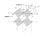
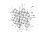
- FIG. 5 is a diagram in which the first detection electrode shown in FIG. 3 and the second detection electrode shown in FIG. 4 are overlapped, and is a plan view showing the wiring configuration of the touch panel substrate. It is a top view which shows the structure of the wiring of the said touchscreen board
- FIG. 18 is a diagram in which the first detection electrode shown in FIG. 16 and the second detection electrode shown in FIG. 17 are overlapped, and is a plan view showing the configuration of the wiring of the touch panel substrate.
- a display device (hereinafter referred to as a display device) having a touch panel function according to an embodiment of the present invention will be described below.
- FIG. 1 is a cross-sectional view illustrating a schematic configuration of a display device according to the present embodiment.
- a display device 1 shown in FIG. 1 includes a touch panel substrate 2, a display panel 3, various drive circuits (data signal line drive circuit, scanning signal line drive circuit, etc .; not shown) that drive the display panel 3, and a backlight. 4 is provided.
- the display panel 3 is an active matrix type liquid crystal display panel in which a liquid crystal layer is sandwiched between an active matrix substrate and a color filter substrate.
- the display panel 3 includes a black matrix (not shown) that partitions each pixel in a grid pattern. Since a general display panel 3 can be used, a detailed description of its structure is omitted.
- the display panel 3 is not limited to a liquid crystal display panel, and an arbitrary display panel such as an organic EL display can be used.
- the backlight 4 is provided on the back side of the display panel 3 and irradiates the display panel 3 with light.
- the touch panel substrate 2 is a capacitive touch panel substrate provided on the front side (user side) of the display panel 3.
- the touch panel substrate 2 includes a substrate 5, a first electrode layer 6, a second electrode layer 7, a first protective layer 8, and a second protective layer 9.
- a first electrode layer 6 is provided on the front side of the substrate 5, and a second electrode layer 7 is provided on the back side of the substrate 5.
- a first protective layer 8 is provided on the front surface side of the first electrode layer 6.
- a second protective layer 9 is provided on the back side of the second electrode layer 7.
- the substrate 5 is formed of a dielectric, and can be formed of, for example, glass or a plastic film.
- the first electrode layer 6 is formed with a plurality of first detection electrodes formed of low resistance conductor wires such as metal. Each first detection electrode extends in the same direction as the direction in which the scanning signal line extends (lateral direction: first direction).
- the second electrode layer 7 is formed with a plurality of second detection electrodes formed of low resistance conductor wires such as metal. Each second detection electrode extends in a direction perpendicular to the direction in which the first detection electrode extends (direction in which the data signal line extends: vertical direction, second direction).
- the first protective layer 8 is a surface with which a detection target object comes into contact, and can be formed of a light-transmitting insulator such as glass or a plastic film.
- the second protective layer 9 can be formed of a light-transmitting insulator such as glass or a plastic film. The second protective layer 9 is adhered on the display panel 3.
- a capacitance is formed between the first detection electrode and the second detection electrode.
- the capacitance value changes.
- the touched position can be specified.
- the first detection electrode may be referred to as a transmission electrode
- the second detection electrode may be referred to as a reception electrode.
- a position detection circuit for detecting the coordinate position of a detection target object a well-known circuit can be used and it is not specifically limited.
- the grid-like metal wiring is arranged at an angle of 0 ° and 90 ° with respect to the scanning signal line, for example. Moiré is likely to occur. If the grid-like metal wiring is arranged at an angle of 45 ° with respect to the scanning signal line, moire is less likely to occur than in the case of 0 ° and 90 °, but moire still often occurs.
- the direction in which the lateral detection electrodes extend is preferably along the scanning signal lines.
- the direction in which the vertical detection electrodes extend is preferably perpendicular to the scanning signal lines. This is because if the direction in which the detection electrode extends is inclined, the contact position cannot be properly detected. Therefore, it is impossible to tilt the touch panel substrate with respect to the display panel together with the detection electrodes in order to tilt the grid-like metal wiring from 45 °.
- FIG. 15 is a plan view showing the arrangement of the first detection electrodes 11 and the second detection electrodes 12 in the touch panel substrate 102 of the reference example.
- a plurality of first grid electrodes 13 and second grid electrodes 14 having a square outer shape are arranged on the touch panel substrate 102.
- the squares showing the outer shapes (regions formed) of the plurality of first grid electrodes 13 and the plurality of second grid electrodes 14 are uniformly inclined.
- the first grid electrode 13 and the second grid electrode 14 are formed in different layers.
- the first grid electrode 13 and the second grid electrode 14 are formed by conductor wires having a square outer shape. Therefore, the light emitted from the display panel can pass through the touch panel substrate 102.
- the pitch of the first detection electrodes 11 and the pitch of the second detection electrodes 12 are the same. Therefore, the position can be detected with the same accuracy both in the vertical direction and in the horizontal direction.
- the pitch of the first detection electrodes 11 and the pitch of the second detection electrodes 12 are determined as specifications based on required performance (detection accuracy, detection resolution).
- the first grid electrodes 13 are spaced apart from each other. Further, the second grid electrodes 14 are spaced apart from each other.
- first grid electrode 13 and the second grid electrode 14 are not shown in FIG. 15, a plurality of the first grid electrodes 13 arranged in the lateral direction are formed in a square region 15 therebetween. Are electrically connected to each other through the connected portions.
- One first detection electrode 11 has a plurality of first grid electrodes 13 arranged in the horizontal direction.
- a plurality of first detection electrodes 11 extending in the horizontal direction are arranged in the vertical direction.
- the plurality of second grid electrodes 14 arranged in the vertical direction apart from each other are electrically connected to each other through another connection portion formed in the square region 15 therebetween.
- One second detection electrode 12 has a plurality of second grid electrodes 14 arranged in the vertical direction.
- a plurality of second detection electrodes 12 extending in the vertical direction are arranged in the horizontal direction.
- Diagonal lines in the first grid electrode 13 are inclined at an angle ⁇ with respect to the direction (lateral direction) in which the first detection electrode 11 extends. However, the first grid electrodes 13 are arranged along the direction in which the first detection electrodes 11 extend. Similarly, a diagonal line (two diagonal lines adjacent to the region 15) in the second grid electrode 14 is inclined at an angle ⁇ with respect to a direction (vertical direction) in which the second detection electrode 12 extends. However, the second grid electrodes 14 are arranged along the direction in which the second detection electrodes 12 extend.
- FIG. 16 is a plan view showing a detailed configuration of the first detection electrode 11.
- the outer shape of each first grid electrode 13 is indicated by a dotted line
- the conductor wire (first conductor line) 17 constituting the first grid electrode 13 is indicated by a solid line.
- Each first detection electrode 11 extends in the lateral direction and has a plurality of first grid electrodes 13.
- the first grid electrodes 13 adjacent in the lateral direction are separated from each other, and a connecting portion 16 formed of a conductor wire is provided therebetween. Adjacent first grid electrodes 13 are connected to each other through the connection portion 16. Note that the first grid electrodes 13 adjacent in the vertical direction are separated from each other.
- the first grid electrode 13 and the connection portion 16 are formed in the same layer (the first electrode layer 6 in FIG. 1).
- the conductor lines 17 in the first grid electrode 13 are formed in a parallel grid shape along the outer shape of the first grid electrode 13. That is, the grid of the conductor lines 17 is formed so that each conductor line 17 is parallel to the outer side (square) side of the first grid electrode 13.
- the conductor wires (grid wiring) 17 constituting the first grid electrode 13 are arranged in a square grid shape.
- the conductor wire 17 and the connecting portion 16 are formed of a low resistance metal or the like.
- the conductor wire of the connecting portion 16 is formed at a position where a part of the lattice-shaped conductor wire (grid wiring) 17 is extended.
- Diagonal lines in the first grid electrode 13 are inclined at an angle ⁇ with respect to the direction (lateral direction) in which the first detection electrode 11 extends. That is, the diagonal line of the unit lattice (minimum unit square) of the lattice forming the first lattice electrode 13 is inclined by an angle ⁇ with respect to the direction (lateral direction) in which the first detection electrode 11 extends.
- the first grid electrodes 13 are arranged along the direction in which the first detection electrodes 11 extend.
- FIG. 17 is a plan view showing a detailed configuration of the second detection electrode 12.
- the outer shape of each second grid electrode 14 is indicated by a dotted line, and a conductor line (second conductor line) 19 constituting the second grid electrode 14 is indicated by a solid line.
- the second detection electrode 12 has the same configuration as that obtained by rotating the first detection electrode 11 by 90 °.
- Each second detection electrode 12 extends in the vertical direction and has a plurality of second grid electrodes 14.
- the second grid electrodes 14 adjacent to each other in the vertical direction are spaced apart from each other, and a connecting portion 18 formed of a conductor wire is provided therebetween. Adjacent second grid electrodes 14 are connected to each other through the connection portion 18. Note that the second grid electrodes 14 adjacent in the horizontal direction are separated from each other.
- the second grid electrode 14 and the connection portion 18 are formed in the same layer (second electrode layer 7 in FIG. 1).
- the conductor wire 19 in the second grid electrode 14 is formed in a parallel grid shape along the outer shape of the second grid electrode 14. That is, the grid of the conductor lines 19 is formed so that each conductor line 19 is parallel to the side of the outer shape (square) of the second grid electrode 14.
- the conductor wires (lattice wiring) 19 constituting the second grid electrode 14 are arranged in a square grid shape.
- the conductor wire 19 and the connecting portion 18 are formed of a low resistance metal or the like. Further, here, the conductor wire of the connecting portion 18 is formed at a position where a part of the lattice-shaped conductor wire (grid wiring) 19 is extended.
- the diagonal lines in the second grid electrode 14 are inclined at an angle ⁇ with respect to the direction (vertical direction) in which the second detection electrode 12 extends. That is, the diagonal of the minimum unit lattice (minimum unit square) of the lattice forming the second lattice electrode 14 is similarly inclined by the angle ⁇ with respect to the direction (vertical direction) in which the second detection electrode 12 extends.
- the second grid electrodes 14 are arranged along the direction in which the second detection electrodes 12 extend.
- FIG. 18 is a diagram in which the first detection electrode 11 shown in FIG. 16 and the second detection electrode 12 shown in FIG. 17 are overlapped, and is a plan view showing the configuration of the wiring of the touch panel substrate 102.
- a uniform lattice pattern is formed on the entire touch panel substrate 102 (a predetermined region where the detection electrodes are formed).
- the conductor lines 17 of the first detection electrodes 11 and the conductor lines 19 of the second detection electrodes are arranged so as not to overlap on the same line. Therefore, the pattern of the 1st detection electrode 11 and the 2nd detection electrode 12 is hard to be visually recognized by a user, and a display quality is not reduced.
- the direction in which the first detection electrode 11 extends (lateral direction) and the direction in which the second detection electrode 12 extends (vertical direction) are orthogonal to each other.
- a line in one direction of a lattice of a black matrix (not shown) formed on the display panel 3 is parallel to a direction (lateral direction) in which the first detection electrode 11 extends, and a line in the other direction is a second line. It is parallel to the direction (longitudinal direction) in which the detection electrode 12 extends.
- the diagonal lines of the unit lattice (minimum unit quadrangle) of the lattice forming the first lattice electrode 13 or the second lattice electrode 14 are the direction in which the first detection electrode 11 extends (lateral direction) and the direction in which the second detection electrode 12 extends ( (Both in the vertical direction). Further, the conductor lines of the lattice are also inclined with respect to both the direction in which the first detection electrode 11 extends (lateral direction) and the direction in which the second detection electrode 12 extends (vertical direction). One of the two diagonal lines of the lattice has an angle ⁇ (0 °) with respect to either the direction in which the first detection electrode 11 extends (lateral direction) or the direction in which the second detection electrode 12 extends (vertical direction). ⁇ ⁇ 45 °) is inclined.
- the pixels of the display panel 3 are arranged in the horizontal and vertical directions.
- the first detection electrode 11 extends in the horizontal direction
- the second detection electrode 12 extends in the vertical direction.
- one diagonal line of the lattice is inclined by an angle ⁇ with respect to the direction in which the first detection electrode 11 extends. That is, the grid-shaped conductor lines are inclined at an angle ⁇ with respect to the 45 ° angle from the scanning signal lines. Therefore, the display device using the touch panel substrate 102 can suppress the occurrence of moire compared to the conventional display device in which the grid-like metal wiring is arranged at an angle of 45 ° with respect to the scanning signal line. it can.
- the grid-shaped conductor lines are inclined with respect to the scanning signal line at an angle of 45 °, and (2) the adjacent first grid electrodes 13 include two wires. Connected by the connecting portion 16 (that is, the width of the connecting portion is the same as the width of one unit cell) (the same applies to the second lattice electrode 14), (3) the first lattice electrode 13 and the second lattice electrode
- the grid electrode 14 is provided with a condition that a uniform grid of conductor lines is formed on the touch panel substrate 102 as shown in FIG.
- the condition (1) is a condition for reducing moire.
- the condition (2) is a condition for the touch panel to function even if a part of the wiring of the connection portion is disconnected.
- the condition (3) is a condition for making the brightness of the entire display screen uniform.
- Grid wiring angle 45 ° ⁇ arctan (1 / m) (1)
- m is the number of grid divisions of the grid electrode, and is a natural number of 2 or more.
- m unit grids separated by the grid wiring are arranged.
- the division number m 8.
- ⁇ shown in FIG. 18 corresponds to arctan (1 / m).
- the angle of the grid wiring is an angle of one grid wiring with respect to the scanning signal line.
- the other grid wiring is perpendicular to one grid wiring.
- the division number m has an appropriate range as a touch panel. For example, if the number of divisions is too large, the area of wiring increases and the transmittance of the touch panel substrate decreases.
- a display device in which a display panel 3 having a pixel pitch of 75 ⁇ m by 225 ⁇ m and a touch panel substrate 102 having a vertical and horizontal sensor axis pitch (detection electrode pitch) of 5 mm is manufactured, We verified whether moiré occurs.
- the touch panel substrate 102 satisfying the above conditions (1) to (3) and the above equation (1) was manufactured by changing the division number m in various ways.
- the combination of the display panel 3 and the touch panel substrate 102 causes moire in any of the manufactured display devices. Since the division number m is a natural number, the angle of the lattice wiring allowed by the above equation (1) is a jump value. For this reason, since the angle of the grid wiring is limited, it is difficult to arrange the grid wiring at an angle at which moire is unlikely to occur.
- the grid wiring angle is set as follows.
- Grid wiring angle 45 ° ⁇ arctan (1 / n) (2)
- n is a real number, and n> m.
- arctan (1 / n) ⁇ arctan (1 / m).
- m is the number of grid divisions of the grid electrode, and is a natural number of 2 or more. That is, in the present embodiment, the angle of the grid wiring is close to 45 ° when the division number m is the same as in the reference example.
- n ⁇ m the size of the square region in the gap between the first lattice electrode and the second lattice electrode is different from the size of one unit lattice determined by the division number m.
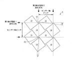
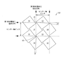
- FIG. 2 is a plan view showing the arrangement of the first detection electrodes 11 and the second detection electrodes 12 in the touch panel substrate 2 of the present embodiment.
- a plurality of first grid electrodes 13 and second grid electrodes 14 having a square outer shape are arranged on the touch panel substrate 2.
- the squares indicating the outer shapes (regions formed) of the plurality of first grid electrodes 13 and the plurality of second grid electrodes 14 are uniformly inclined.
- the first grid electrode 13 and the second grid electrode 14 are formed in different layers. Further, the first grid electrode 13 and the second grid electrode 14 are formed in different regions in plan view.
- the first grid electrode 13 and the second grid electrode 14 are formed by conductor wires having a square outer shape. Therefore, the light emitted from the display panel can pass through the touch panel substrate 2.
- the pitch of the first detection electrodes 11 and the pitch of the second detection electrodes 12 are the same. Therefore, the position can be detected with the same accuracy both in the vertical direction and in the horizontal direction.
- the pitch of the first detection electrodes 11 and the pitch of the second detection electrodes 12 are determined as specifications based on required performance (detection accuracy, detection resolution). Therefore, the pitch of the first detection electrodes 11 and the pitch of the second detection electrodes 12 (that is, the pitch of the sensor shaft) are the same as those in the reference example shown in FIG.
- the first grid electrodes 13 are spaced apart from each other. Further, the second grid electrodes 14 are spaced apart from each other.
- the external shape of the 1st grid electrode 13 and the 2nd grid electrode 14 becomes a rhombus.
- the first grid electrode 13 and the second grid electrode 14 are formed by conductor lines formed in a rhombus grid shape.
- first grid electrode 13 and the second grid electrode 14 are not shown in FIG. 2, a plurality of the first grid electrodes 13 arranged in the lateral direction are formed in a square region 15 therebetween. Are electrically connected to each other through the connected portions.
- One first detection electrode 11 has a plurality of first grid electrodes 13 arranged in the horizontal direction.
- a plurality of first detection electrodes 11 extending in the horizontal direction are arranged in the vertical direction.
- the plurality of second grid electrodes 14 arranged in the vertical direction apart from each other are electrically connected to each other through another connection portion formed in the square region 15 therebetween.
- One second detection electrode 12 has a plurality of second grid electrodes 14 arranged in the vertical direction.
- a plurality of second detection electrodes 12 extending in the vertical direction are arranged in the horizontal direction.
- Diagonal lines in the first grid electrode 13 are inclined at an angle ⁇ with respect to the direction (lateral direction) in which the first detection electrode 11 extends.
- ⁇ arctan (1 / n).
- the first grid electrodes 13 are arranged along the direction in which the first detection electrodes 11 extend.
- a diagonal line (two diagonal lines adjacent to the region 15) in the second grid electrode 14 is inclined at an angle ⁇ with respect to a direction (vertical direction) in which the second detection electrode 12 extends.
- the second grid electrodes 14 are arranged along the direction in which the second detection electrodes 12 extend.
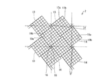
- FIG. 3 is a plan view showing a detailed configuration of the first detection electrode 11 in the first electrode layer 6.
- the outline of each first grid electrode 13 is indicated by a dotted line, and the conductor lines (first conductor line, second conductor line) 17a and 17b constituting the first grid electrode 13 are indicated by solid lines.
- the angle of the lattice wiring of this embodiment is the same as the angle of the reference example. However, since the number m of grid electrode divisions is different from the reference example, the pitch of the grid wiring of this embodiment is different from the reference example.
- Each first detection electrode 11 extends in the lateral direction and has a plurality of first grid electrodes 13.
- the first grid electrodes 13 that are adjacent in the horizontal direction are spaced apart from each other, and a connecting portion (first connecting portion) 16 is provided therebetween.
- the first grid electrode 13 includes a plurality of conductor lines 17a and a plurality of conductor lines 17b.
- the plurality of conductor lines 17a are parallel to each other and inclined at an angle ⁇ with respect to the direction (lateral direction) in which the first detection electrode 11 extends.
- ⁇ 45 ° ⁇ .
- ⁇ is greater than 0 ° and less than 45 °. Since 2 ⁇ m ⁇ n, 45 ° ⁇ arctan (1/2) ⁇ ⁇ 45 °.
- the plurality of conductor lines 17b are parallel to each other and perpendicular to the conductor line 17a.
- the plurality of conductor lines 17 a and the plurality of conductor lines 17 b are formed in a parallel grid shape along the outer shape of the first grid electrode 13.
- the grids of the conductor lines 17a and 17b are formed so that the conductor lines 17a and 17b are parallel to the outer side (square) side of the first grid electrode 13.
- the conductor wires (grid wirings) 17a and 17b constituting the first grid electrode 13 are arranged in a square grid shape. That is, the pitch of the plurality of conductor lines 17a is the same as the pitch of the plurality of conductor lines 17b.
- connection portion 16 includes a plurality of conductor wires (fifth conductor wires) 21. Adjacent first grid electrodes 13 are connected to each other through the conductor wire 21 of the connecting portion 16. The plurality of conductor lines 21 are parallel to the conductor line 17a.
- the connecting portion 16 has two conductor wires, but the connecting portion 16 may have a configuration having three or more conductor wires 21.
- first grid electrodes 13 adjacent in the vertical direction are separated from each other.
- the first grid electrode 13 and the connection portion 16 are formed in the same layer (the first electrode layer 6 in FIG. 1).
- the conductor wires 17a and 17b and the conductor wire 21 are made of a light-shielding low-resistance metal or the like.
- the pitch of the plurality of conductor wires 21 of the connecting portion 16 is different from the pitch of the grid wiring 17a constituting the first grid electrode 13. This is because when n ⁇ m, the size of the square region 15 (see FIG. 2) in the gap between the first lattice electrode 13 and the second lattice electrode 14 is equal to that of one unit lattice of the first lattice electrode 13. This is because the size is different. In the present embodiment, since n> m, the pitch of the two conductor wires 21 included in the connection portion 16 is smaller than the pitch of the conductor wires 17a constituting the first lattice electrode 13.
- one conductor line 21 of the connection part 16 extends along the conductor line 17a of the left first grid electrode 13 (aligned with the conductor line 17a), and the other conductor line 21 of the connection part 16 is provided. Extends along the conductor line 17a of the first grid electrode 13 on the right side. Note that the positions of the conductor lines 17a of the two adjacent first grid electrodes 13 are not aligned (do not line up in a straight line).
- Diagonal lines in the first grid electrode 13 are inclined at an angle ⁇ with respect to the direction (lateral direction) in which the first detection electrode 11 extends. That is, the diagonal line of the unit lattice (minimum unit square) of the lattice forming the first lattice electrode 13 is inclined by an angle ⁇ with respect to the direction (lateral direction) in which the first detection electrode 11 extends.
- the first grid electrodes 13 are arranged along the direction in which the first detection electrodes 11 extend (lateral sensor axes).
- the first grid electrode 13 and the grid-shaped conductor wires (grid wiring) 17a and 17b constituting the first grid electrode 13 are formed to be inclined at a predetermined angle, and are spaced apart and adjacent to the first grid.
- the electrodes 13 are connected to each other by the connecting portion 16.
- the conductor wires (grid wires) 17a and 17b forming the lattice from ⁇ 45 ° by ⁇ arctan (1 / n)
- the lattice wires 17a and 17b can be arranged at an angle at which moiré is unlikely to occur.
- the grid lines 17a of the adjacent first grid electrodes 13 are not aligned, but by making the pitch of the conductor lines 21 of the connecting portion 16 smaller than the pitch of the grid lines 17a, at least two conductor lines 21 are used. Adjacent first grid electrodes 13 can be connected to each other. For this reason, even if one conductor wire 21 of the connection portion 16 is disconnected, the other conductor wire 21 maintains the electrical connection.
- FIG. 4 is a plan view showing a detailed configuration of the second detection electrode 12 in the second electrode layer 7.
- the outer shape of each second grid electrode 14 is indicated by a dotted line
- the conductor lines (third conductor line, fourth conductor line) 19a and 19b constituting the second grid electrode 14 are indicated by solid lines.
- the second detection electrode 12 has the same configuration as that obtained by rotating the first detection electrode 11 by 90 °.
- Each second detection electrode 12 extends in the vertical direction and has a plurality of second grid electrodes 14.
- the second grid electrodes 14 adjacent in the vertical direction are separated from each other, and a connecting portion (second connecting portion) 18 is provided therebetween.
- the second grid electrode 14 includes a plurality of conductor lines 19a and a plurality of conductor lines 19b.
- the plurality of conductor lines 19a are parallel to each other and inclined at an angle ⁇ with respect to the direction (vertical direction) in which the second detection electrode 12 extends.
- the plurality of conductor lines 19b are parallel to each other and perpendicular to the conductor line 19a.
- the plurality of conductor lines 19 a and the plurality of conductor lines 19 b are formed in a lattice shape parallel to the outer shape of the second lattice electrode 14. That is, the grids of the conductor lines 19a and 19b are formed so that the conductor lines 19a and 19b are parallel to the outer side (square) side of the second grid electrode 14.
- the conductor wires (lattice wirings) 19a and 19b constituting the second grid electrode 14 are arranged in a square grid shape. That is, the pitch of the plurality of conductor lines 19a is the same as the pitch of the plurality of conductor lines 19b.
- the connecting portion 18 includes a plurality of conductor wires (sixth conductor wires) 22. Adjacent second grid electrodes 14 are connected to each other through the conductor wire 22 of the connecting portion 18. The plurality of conductor lines 22 are parallel to the conductor line 19a. In the present embodiment, the connecting portion 18 has two conductor lines, but the connecting portion 18 may have three or more conductor wires 22.
- second grid electrodes 14 adjacent in the horizontal direction are separated from each other.
- the second grid electrode 14 and the connection portion 18 are formed in the same layer (second electrode layer 7 in FIG. 1).
- the conductor wires 19a and 19b and the conductor wire 22 are made of a light-shielding low-resistance metal or the like.
- the pitch of the plurality of conductor lines 22 in the connecting portion 18 is different from the pitch of the grid wiring 19a constituting the second grid electrode 14.
- the pitch of the two conductor wires 22 included in the connecting portion 18 is smaller than the pitch of the conductor wires 19a constituting the second grid electrode 14.
- one conductor line 22 of the connection part 18 extends along the conductor line 19a of the upper second grid electrode 14 (aligned with the conductor line 19a), and the other conductor line 22 of the connection part 18 is present. Extends along the conductor line 19a of the lower second grid electrode. Note that the positions of the conductor lines 19a of the two second grid electrodes 14 adjacent to each other are not aligned (not aligned in a straight line).
- the diagonal lines in the second grid electrode 14 are inclined at an angle ⁇ with respect to the direction (vertical direction) in which the second detection electrode 12 extends. That is, the diagonal of the unit lattice (minimum unit quadrilateral) of the lattice forming the second lattice electrode 14 is similarly inclined by the angle ⁇ with respect to the direction (vertical direction) in which the second detection electrode 12 extends. However, the respective second grid electrodes 14 are arranged along the direction in which the second detection electrodes 12 extend (longitudinal sensor axis).
- FIG. 5 is a diagram in which the first detection electrode 11 shown in FIG. 3 and the second detection electrode 12 shown in FIG. 4 are overlapped, and is a plan view showing the configuration of the wiring of the touch panel substrate 2.
- One angled conductor line 17a (upward-facing grid line) forming the grid of the first grid electrode 13 and one angled conductor line 19b (upward-right grid line) forming the grid of the second grid electrode 14; Are parallel.
- the other angle conductor line 17b (right-down grid wiring) forming the grid of the first grid electrode 13 and the other angle conductor line 19a (right-down grid wiring) forming the grid of the second grid electrode 14; Are parallel.
- the first detection electrode 11 and the second detection electrode 12 do not form a uniform lattice pattern. This is because the grid lines of the first grid electrode 13 and the second grid electrode 14 adjacent to each other are not aligned. For example, in the first grid electrode 13 and the second grid electrode 14 that are adjacent to each other in the direction in which the conductor line 17a extends (third direction), the conductor line 17a and the conductor line 19b parallel to the conductor line 17a are not aligned. Moreover, in the 1st grid
- the transmittance of the touch panel substrate 2 is uniform.
- the pitch of the conductor lines of the connecting portions 16 and 18 is different from the pitch of the grid lines of the first grid electrode 13 and the second grid electrode 14.
- the area where the connection portions 16 and 18 are formed is a very small part of the entire screen and the difference in wiring density is not large, nonuniformity in transmittance (that is, brightness) is visually recognized. There is no.
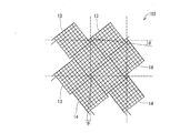
- FIG. 6 is a diagram showing a wiring configuration of the touch panel substrate 2 excluding the lines indicating the reference numerals and the sensor axes. As shown in FIG. 6, the difference between the region where the connection portion is arranged and the region where the grid wiring is formed is hardly visible.
- the conductor lines 17a and 17b of the first detection electrode 11, the conductor lines 19a and 19b of the second detection electrode, and the conductor lines of the connection portions 16 and 18 are arranged so as not to overlap on the same line. For this reason, even if the patterns of the first detection electrode 11 and the second detection electrode 12 are shifted in the manufacturing process, the shift of the pattern is not easily recognized by the user, and the display quality is not deteriorated.
- the direction in which the first detection electrode 11 extends (lateral direction) and the direction in which the second detection electrode 12 extends (vertical direction) are orthogonal to each other.
- a line in one direction of a lattice of a black matrix (not shown) formed on the display panel 3 is parallel to a direction (lateral direction) in which the first detection electrode 11 extends, and a line in the other direction is a second line. It is parallel to the direction (longitudinal direction) in which the detection electrode 12 extends.
- the diagonal lines of the unit lattice (minimum unit quadrangle) of the lattice forming the first lattice electrode 13 or the second lattice electrode 14 are the direction in which the first detection electrode 11 extends (lateral direction) and the direction in which the second detection electrode 12 extends ( (Both in the vertical direction). Further, the conductor lines of the lattice are also inclined with respect to both the direction in which the first detection electrode 11 extends (lateral direction) and the direction in which the second detection electrode 12 extends (vertical direction). One of the two diagonal lines of the lattice is inclined at an angle ⁇ with respect to either the direction in which the first detection electrode 11 extends (lateral direction) or the direction in which the second detection electrode 12 extends (vertical direction). .
- the conductor lines 17a and 17b of the first detection electrode 11 may be extended so that the conductor lines 19a and 19b of the second detection electrode partially overlap, or the first detection electrodes 11 may be connected to each other. In order to avoid conduction, some conductor wires may be removed. Further, the number of grid lines and the like can be appropriately changed so as to equally divide the lengths of the outer sides of the first grid electrode 13 and the second grid electrode 14.
- FIG. 7 is a diagram showing the overlay of the touch panel substrate 2 and the display panel 3.
- a grid-like black matrix 10 that partitions pixels is formed on the display panel 3.
- the black matrix 10 is formed of a light shield.
- the first detection electrode 11 extends in the horizontal direction
- the second detection electrode 12 extends in the vertical direction.
- one diagonal line of the lattice is inclined by an angle ⁇ with respect to the direction in which the first detection electrode 11 extends.
- the inclination of the grid wiring (that is, the diagonal angle of the grid) is determined by n. Since n> m and n is a parameter that can be set independently from the division number m, the inclination of the lattice wiring can be determined independently from the division number m. Therefore, the grid wiring of the adjacent first grid electrode 13 and the grid wiring of the second grid electrode 14 are not aligned in a straight line (see FIG. 5).
- the pitch of the conductor lines of the connection portions 16 and 18 is different from the pitch of the grid wirings 17a, 17b, 19a, and 19b, thereby connecting the grid electrodes to each other with two conductor lines and transmitting through the touch panel substrate 2.
- the first detection electrode 11 extends in the same direction (lateral direction) as the scanning signal line, and the second detection electrode 12 extends in the vertical direction (vertical direction) with respect to the scanning signal line. Therefore, the display device 1 can suppress the occurrence of moire and can appropriately detect the contact position.
- the first grid electrode 13 and the second grid electrode 14 are formed to be inclined together with the grid wiring in the first grid electrode 13.
- the connecting portions 16 and 18 are formed in the gap (region 15) generated between the second grid electrodes 14.
- the lattice wirings 17a, 17b, 19a, and 19b occupy most of the wiring pattern. Therefore, the pitch of the conductor wires of the connecting portions 16 and 18 is made different from the pitch of the grid wires 17a, 17b, 19a, and 19b of the first grid electrode 13 and the second grid electrode 14, thereby providing the grid wires 17a, 17b, and 19a.
- the degree of freedom of the pitch of 19b and the degree of freedom of the angle ⁇ of the lattice wiring can be increased.
- the conductor wire pitch of the connecting portion is L ⁇ (1 / n)
- the pitch of the grid wiring is L ⁇ (1 / m ). That is, the ratio between the pitch of the conductor wire of the connecting portion and the pitch of the lattice wiring is m: n (where m ⁇ n). In order to prevent moiré from occurring, it is preferable that m ⁇ n.
- n becomes large, it means that the pitch of the conductor wire of a connection part becomes small compared with the pitch of lattice wiring.
- the pitch of the conductor wire of the connecting portion is larger than half of the pitch of the lattice wiring, that is, n ⁇ 2 m.
- the laminated structure of the touch panel substrate, the pitch of each sensor axis, and the arrangement of the first and second grid electrodes are the same as those in the first embodiment (FIGS. 1 and 2).
- FIG. 8 is a plan view showing a detailed configuration of the first detection electrode 11 in the first electrode layer 6 of the present embodiment.
- the outer shape of each first grid electrode 13 is indicated by a dotted line, and conductor wires (first conductor wire, second conductor wire, seventh conductor wire) 17a, 17b, and 17c constituting the first grid electrode 13 are shown. It is shown with a solid line.
- the angle of the grid wiring of this embodiment is the same as that of the first embodiment.
- the first grid electrode 13 includes a plurality of conductor lines 17a, a plurality of conductor lines 17b, and a plurality of conductor lines 17c.
- the plurality of conductor lines 17b are parallel to each other and perpendicular to the conductor line 17a.
- the plurality of conductor lines 17 a, the plurality of conductor lines 17 b, and the plurality of conductor lines 17 c are formed in a parallel grid shape along the outer shape of the first grid electrode 13. That is, the grids of the conductor lines 17a, 17b, and 17c are formed so that the conductor lines 17a, 17b, and 17c are parallel to the outer side (square) side of the first grid electrode 13.
- the pitch of the plurality of conductor lines 17a and the pitch of the plurality of conductor lines 17b are the same. However, the pitch of the plurality of conductor lines 17a is different from the pitch of the plurality of conductor lines 17c.
- connection portion 16 includes a plurality of conductor wires (fifth conductor wires) 21.
- the plurality of conductor wires 21 are parallel to the conductor wires 17a and 17c.
- the connection portion 16 has two conductor wires 21.
- the conductor wires 17a, 17b, 17c and the conductor wire 21 are made of a light-shielding low-resistance metal or the like.
- the pitch of the plurality of conductor wires 21 of the connecting portion 16 is the same as the pitch of the plurality of conductor wires 17c constituting the first lattice electrode 13.
- the plurality of conductor lines 17 c constituting the first grid electrode 13 are formed so as to be in line with the plurality of conductor lines 21 of the connection portion 16. Therefore, the positions of the conductor lines 17c of the two first grid electrodes 13 adjacent to each other are aligned.
- the first grid electrode 13 and the grid-shaped conductor wires 17a to 17c constituting the first grid electrode 13 are formed so as to be inclined at a predetermined angle, and the first grid electrodes 13 that are adjacent to each other apart from each other are formed.
- the connection is made by the connection unit 16.
- the conductor wires 17a, 17b, and 17c forming the lattice are inclined by ⁇ arctan (1 / n) from 45 °, so that the conductor wires 17a, 17b, and 17c can be arranged at an angle at which moiré is unlikely to occur. Since m ⁇ n, the conductor lines 17a of the adjacent first grid electrodes 13 are not aligned.
- the conductor wire 21 and the lattice of the connecting portion 16 are arranged. Can be aligned with the conductor wire 17c forming the.
- the angle of these conductor wires 17a to 17c can be adjusted while the sensor axis remains in the horizontal direction. It is possible to realize a touch panel substrate that reduces the occurrence of the above.
- FIG. 9 is a plan view showing a detailed configuration of the second detection electrode 12 in the second electrode layer 7.
- the outline of each second grid electrode 14 is indicated by a dotted line, and conductor wires (third conductor line, fourth conductor line, seventh conductor line) 19a, 19b, 19c constituting the second grid electrode 14 are shown. It is shown with a solid line.
- the second detection electrode 12 has the same configuration as that obtained by rotating the first detection electrode 11 of FIG. 8 by 90 °.
- the second grid electrode 14 includes a plurality of conductor lines 19a, a plurality of conductor lines 19b, and a plurality of conductor lines 19c.
- the plurality of conductor lines 19b are parallel to each other and perpendicular to the conductor line 19a.
- the plurality of conductor lines 19 a, the plurality of conductor lines 19 b, and the plurality of conductor lines 17 c are formed in a lattice shape parallel to the outer shape of the second lattice electrode 14. That is, the grids of the conductor lines 19a, 19b, and 19c are formed so that the conductor lines 19a, 19b, and 19c are parallel to the outer side (square) side of the second grid electrode 14.
- the pitch of the plurality of conductor lines 19a and the pitch of the plurality of conductor lines 19b are the same. However, the pitch of the plurality of conductor wires 19a is different from the pitch of the plurality of conductor wires 19c.
- the connecting portion 18 includes a plurality of conductor wires (sixth conductor wires) 22.
- the plurality of conductor lines 22 are parallel to the conductor lines 19a and 19c.
- the connection portion 18 has two conductor wires 22.
- the conductor wires 19a, 19b, 19c and the conductor wire 22 are formed of a light-shielding low-resistance metal or the like.
- the pitch of the plurality of conductor wires 22 of the connecting portion 18 is the same as the pitch of the plurality of conductor wires 19c constituting the second grid electrode 14.
- the plurality of conductor lines 19 c constituting the second grid electrode 14 are formed so as to be in line with the plurality of conductor lines 22 of the connection portion 18. Therefore, the positions of the conductor lines 19c of the two adjacent second grid electrodes 14 are aligned.
- the second grid electrode 14 and the grid-shaped conductor wires 19a to 19c constituting the second grid electrode 14 are formed so as to be inclined at a predetermined angle, and the adjacent second grid electrodes 14 separated from each other are formed.
- the connection is made by the connection unit 18.
- the conductor wires 19a to 19c can be arranged at an angle at which moiré is unlikely to occur. Since m ⁇ n, the conductor lines 19a of the adjacent second grid electrodes 14 are not aligned.
- the conductor wire 22 and the lattice of the connecting portion 18 are arranged. Can be aligned with the conductor wire 19c forming the.
- FIG. 10 is a diagram in which the first detection electrode 11 shown in FIG. 8 and the second detection electrode 12 shown in FIG. 9 are overlapped, and is a plan view showing the configuration of the wiring of the touch panel substrate 20 of the present embodiment.
- the conductor wire 19c is parallel.
- the first detection electrode 11 and the second detection electrode 12 do not form a uniform lattice pattern. This is because the grid lines of the first grid electrode 13 and the second grid electrode 14 adjacent to each other are not aligned. For example, in the first grid electrode 13 and the second grid electrode 14 that are adjacent to each other in the direction in which the conductor line 17a extends (third direction), the conductor line 17a and the conductor line 19b parallel to the conductor line 17a are not aligned. Moreover, in the 1st grid
- the pitch of the conductor wire 17c, the pitch of the conductor wire 19c, and the pitch of the conductor wires of the connecting portions 16 and 18 are determined as the main conductor wires 17a and 17a forming the lattice of the first lattice electrode 13 and the second lattice electrode 14, respectively. It is different from the pitches of 17b, 19a and 19b. However, the region in which the conductor wire 17c, the conductor wire 19c, and the conductor wires of the connection portions 16 and 18 are formed is smaller than the region in which the conductor wires 17a, 17b, 19a, and 19b are formed.
- the first pitch conductor line 17 a and the second pitch conductor line 17 c are formed as the right-upward wiring, while the first pitch conductor line is formed as the right-down wiring. Only 17b is formed. Therefore, as in the first embodiment, there is a sufficient effect of suppressing the occurrence of moire.
- the conductor lines 17a to 17c of the first detection electrode 11, the conductor lines 19a to 19c of the second detection electrode, and the conductor lines of the connecting portions 16 and 18 are arranged so as not to overlap on the same line. For this reason, even if the patterns of the first detection electrode 11 and the second detection electrode 12 are shifted in the manufacturing process, the shift of the pattern is not easily recognized by the user, and the display quality is not deteriorated.
- the direction in which the first detection electrode 11 extends (lateral direction) and the direction in which the second detection electrode 12 extends (vertical direction) are orthogonal to each other.
- the laminated structure of the touch panel substrate, the pitch of each sensor axis, and the arrangement of the first and second grid electrodes are the same as those in the first embodiment (FIGS. 1 and 2).
- FIG. 11 is a plan view showing a detailed configuration of the first detection electrode 11 in the first electrode layer 6 of the present embodiment.
- the outer shape of each first grid electrode 13 is indicated by a dotted line, and conductor lines (first conductor line, second conductor line, seventh conductor line) 17 a, 17 b, and 17 c constituting the first grid electrode 13 are shown. It is shown with a solid line.
- the angle of the grid wiring of this embodiment is the same as that of the first embodiment.
- the first grid electrode 13 includes a plurality of conductor lines 17a and a plurality of conductor lines 17b.
- the plurality of conductor lines 17b are parallel to each other and perpendicular to the conductor line 17a.
- the plurality of conductor lines 17 a and the plurality of conductor lines 17 b are formed in a parallel grid shape along the outer shape of the first grid electrode 13.
- the grids of the conductor lines 17a and 17b are formed so that the conductor lines 17a and 17b are parallel to the outer side (square) side of the first grid electrode 13.
- the pitch of the plurality of conductor lines 17a and the pitch of the plurality of conductor lines 17b are the same.
- the pitch of the plurality of conductor wires 21 of the connecting portion 16 is different from the pitch of the grid wiring 17a constituting the first grid electrode 13.
- the pitch of the two conductor wires 21 included in the connection portion 16 is smaller than the pitch of the conductor wires 17a constituting the first lattice electrode 13.
- one conductor line 21 of the connection part 16 extends along the conductor line 17a of the left first grid electrode 13 (aligned with the conductor line 17a), and the other conductor line 21 of the connection part 16 is provided. Extends along the conductor line 17a of the first grid electrode 13 on the right side. Note that the positions of the conductor lines 17a of the two adjacent first grid electrodes 13 are not aligned (do not line up in a straight line).
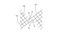
- FIG. 12 is an enlarged view of the periphery of the connecting portion 16 in FIG.
- the connecting portion 16 includes a plurality of conductor wires (fifth conductor wires) 21 and a plurality of conductor wires (eighth conductor wires) 23.
- the plurality of conductor lines 21 are parallel to the conductor line 17a.
- the plurality of conductor lines 23 are parallel to the conductor line 17b. That is, the conductor line 23 is perpendicular to the conductor line 21.
- the connection portion 16 includes two conductor wires 21 and two conductor wires 23.
- the conductor wire 21 on the upper side of the connecting portion 16 and the conductor wire 17a of the first grid electrode 13 adjacent to the left thereof are not aligned with each other.
- the conductor lines 21 and the conductor lines 17a that are not aligned are connected by a conductor line 23 on the left side of the connection portion 16.
- the conductor line 21 on the lower side of the connecting part 16 and the conductor line 17a of the first grid electrode 13 adjacent to the right side thereof are connected by the conductor line 23 on the right side of the connecting part 16.
- the conductor wire 23 of the connecting portion 16 is formed at a position overlapping the line on which the conductor wire of the second grid electrode is formed.
- the conductor wires 17a and 17b and the conductor wires 21 and 23 are made of a light-shielding low-resistance metal or the like.
- the first grid electrode 13 and the grid-shaped conductor wires (grid wiring) 17a and 17b constituting the first grid electrode 13 are formed to be inclined at a predetermined angle, and are spaced apart and adjacent to the first grid.
- the electrodes 13 are connected to each other by the connecting portion 16.
- the lattice wires 17a and 17b can be arranged at an angle at which moiré is unlikely to occur. Since m ⁇ n, the lattice wirings 17a of the adjacent first lattice electrodes 13 are not aligned.
- the pitch of the conductor wires 21 of the connecting portion 16 is made smaller than the pitch of the lattice wiring 17a and connecting the conductor wires 21 and the lattice wiring 17a with the conductor wires 23 perpendicular to the conductor wires 21, the at least two sets of conductor wires 21 are connected.
- the adjacent first grid electrodes 13 can be connected by the conductor wires 21 and 23. Therefore, even if one conductor wire 21/23 of the connection part 16 is disconnected, the electrical connection is maintained by the other conductor wire 21/23.
- the extended conductor wire 21 is used in order to reduce the possibility of disconnection during manufacturing.
- the conductor wires 23 may be crossed (in a cross).
- FIG. 13 is a plan view showing a detailed configuration of the second detection electrode 12 in the second electrode layer 7.
- the outline of each second grid electrode 14 is indicated by a dotted line, and the conductor lines (third conductor line, fourth conductor line) 19a and 19b constituting the second grid electrode 14 are indicated by solid lines.
- the second detection electrode 12 has the same configuration as that obtained by rotating the first detection electrode 11 by 90 °.
- the second grid electrode 14 includes a plurality of conductor lines 19a and a plurality of conductor lines 19b.
- the plurality of conductor lines 19a are parallel to each other and inclined at an angle ⁇ with respect to the direction (vertical direction) in which the second detection electrode 12 extends.
- the plurality of conductor lines 19b are parallel to each other and perpendicular to the conductor line 19a.
- the plurality of conductor lines 19 a and the plurality of conductor lines 19 b are formed in a lattice shape parallel to the outer shape of the second lattice electrode 14. That is, the grids of the conductor lines 19a and 19b are formed so that the conductor lines 19a and 19b are parallel to the outer side (square) side of the second grid electrode 14.
- the pitch of the plurality of conductor lines 19a and the pitch of the plurality of conductor lines 19b are the same.
- the pitch of the plurality of conductor lines 22 in the connecting portion 18 is different from the pitch of the grid wiring 19a constituting the second grid electrode 14.
- the pitch of the two conductor wires 22 included in the connecting portion 18 is smaller than the pitch of the conductor wires 19a constituting the second grid electrode 14.
- one conductor line 22 of the connection part 18 extends along the conductor line 19a of the upper second grid electrode 14 (aligned with the conductor line 19a), and the other conductor line 22 of the connection part 18 is present. Extends along the conductor line 19a of the lower second grid electrode. Note that the positions of the conductor lines 19a of the two second grid electrodes 14 adjacent to each other are not aligned (not aligned in a straight line).
- the connecting portion 18 includes a plurality of conductor lines (sixth conductor lines) 22 and a plurality of conductor lines (eighth conductor lines) 24.
- the plurality of conductor lines 22 are parallel to the conductor line 19a.
- the plurality of conductor lines 24 are parallel to the conductor line 19b. That is, the conductor line 24 is perpendicular to the conductor line 22.
- the connecting portion 18 includes two conductor wires 22 and two conductor wires 24.
- the conductor wire 22 on the right side of the connecting portion 18 and the conductor wire 19a of the second grid electrode 14 adjacent on the conductor wire 22 are not aligned with each other.
- the conductor line 22 and the conductor line 19a that are not aligned are connected by a conductor line 24 on the upper side of the connecting portion 18.
- the conductor wire 22 on the left side of the connecting portion 18 and the conductor wire 19a of the second grid electrode 14 adjacent below the conductor wire 22 are connected by the conductor wire 24 on the lower side of the connecting portion 18.
- the conductor wire 24 of the connecting portion 18 is formed at a position overlapping the line on which the conductor wire of the first grid electrode is formed.
- the conductor wires 19a and 19b and the conductor wires 22 and 24 are made of a light-shielding low-resistance metal or the like.
- the second grid electrode 14 and the grid-shaped conductor wires (lattice wirings) 19a and 19b constituting the second grid electrode 14 are formed to be inclined at a predetermined angle, and are spaced apart and adjacent to the second grid.
- the electrodes 14 are connected to each other by a connecting portion 18.
- the conductor wires (lattice wirings) 19a and 19b forming the lattice from ⁇ 45 ° by ⁇ arctan (1 / n) the lattice wirings 19a and 19b can be arranged at an angle at which moire is unlikely to occur.
- the lattice wirings 19a of the adjacent second lattice electrodes 14 are not aligned.
- the pitch of the conductor wire 22 of the connecting portion 18 is made smaller than the pitch of the grid wiring 19a and connecting the conductor wire 22 and the grid wiring 19a by the conductor wire 24 perpendicular thereto, at least two sets.
- the adjacent second grid electrodes 14 can be connected by the conductor wires 22 and 24. For this reason, even if one of the conductor wires 22 and 24 of the connecting portion 18 is disconnected, the electrical connection is maintained by the other conductor wires 22 and 24.
- FIG. 14 is a diagram in which the first detection electrode 11 shown in FIG. 11 and the second detection electrode 12 shown in FIG. 13 are overlapped, and is a plan view showing the wiring configuration of the touch panel substrate 20 of the present embodiment.
- One angled conductor line 17a (upward-facing grid line) forming the grid of the first grid electrode 13 and one angled conductor line 19b (upward-right grid line) forming the grid of the second grid electrode 14; Are parallel.
- the other angle conductor line 17b (right-down grid wiring) forming the grid of the first grid electrode 13 and the other angle conductor line 19a (right-down grid wiring) forming the grid of the second grid electrode 14; Are parallel.
- the first detection electrode 11 and the second detection electrode 12 do not form a uniform lattice pattern. This is because the grid lines of the first grid electrode 13 and the second grid electrode 14 adjacent to each other are not aligned. For example, in the first grid electrode 13 and the second grid electrode 14 that are adjacent to each other in the direction in which the conductor line 17a extends (third direction), the conductor line 17a and the conductor line 19b parallel to the conductor line 17a are not aligned. Moreover, in the 1st grid
- the transmittance of the touch panel substrate 30 is uniform.
- the pitch of the conductor lines of the connecting portions 16 and 18 is different from the pitch of the grid wirings 17 a, 17 b, 19 a, and 19 b of the first grid electrode 13 and the second grid electrode 14.
- the area where the connection portions 16 and 18 are formed is a very small part of the entire screen and the difference in wiring density is not large, nonuniformity in transmittance (that is, brightness) is visually recognized. There is no.
- the conductor wire 23 of the connection portion 16 overlaps the conductor wire 19a of the second grid electrode 14 on the extension line of the conductor wire 22 of the connection portion 18.
- the conductor line 24 of the connection part 18 overlaps the conductor line 17a of the first grid electrode 13 on the extension line of the conductor line 21 of the connection part 16.
- the division number m is large and the pitch of the plurality of conductor lines 17a of the first grid electrode 13 and the plurality of conductor lines 19a of the second grid electrode 14 are smaller than the pitch of the plurality of conductor lines of the connecting portions 16 and 18.
- the conductor wire 23 of the connecting portion 16 overlaps the conductor wire 22 of the connecting portion 18, and the conductor wire 24 of the connecting portion 18 overlaps the conductor wire 21 of the connecting portion 16.
- the diagonal lines of the unit lattice (minimum unit quadrangle) of the lattice forming the first lattice electrode 13 or the second lattice electrode 14 are the direction in which the first detection electrode 11 extends (lateral direction) and the direction in which the second detection electrode 12 extends ( (Both in the vertical direction). Further, the conductor lines of the lattice are also inclined with respect to both the direction in which the first detection electrode 11 extends (lateral direction) and the direction in which the second detection electrode 12 extends (vertical direction). One of the two diagonal lines of the lattice is inclined at an angle ⁇ with respect to either the direction in which the first detection electrode 11 extends (lateral direction) or the direction in which the second detection electrode 12 extends (vertical direction). .
- the first grid electrode 13 and the second grid electrode 14 are formed so as to be tilted together with the grid wiring therein, and a gap (region 15) generated between the first grid electrode 13 and the second grid electrode 14 is formed.
- Connection portions 16 and 18 are formed.
- the lattice wirings 17a, 17b, 19a, and 19b occupy most of the wiring pattern. Therefore, the pitch of the conductor wires of the connecting portions 16 and 18 is made different from the pitch of the grid wires 17a, 17b, 19a, and 19b of the first grid electrode 13 and the second grid electrode 14, thereby providing the grid wires 17a, 17b, and 19a.
- the region where the wiring pitch is small is smaller than that of the first embodiment (FIG. 5).
- the touch panel substrate 30 compared with touch panel substrate 2 of Embodiment 1 (Drawing 5) the field where the density of wiring is more uniform is large. Therefore, the touch panel substrate 30 has a uniform transmittance and can further suppress the generation of moire.
- a touch panel substrate is arranged along a second direction different from the first direction, and a first detection electrode having a plurality of first grid electrodes arranged along the first direction.
- a plurality of second grid electrodes, and the plurality of first grid electrodes and the plurality of second grid electrodes are formed in different regions in plan view, and each first grid electrode Includes a plurality of first conductor lines parallel to a third direction and a plurality of second conductor lines parallel to a fourth direction different from the third direction, and the plurality of first conductor lines and the plurality of first conductor lines.
- the two conductor lines form a grid, and the third direction is inclined with respect to the first direction by an angle ⁇ , and 0 ° ⁇ ⁇ 45 °.
- the plurality of third conductor lines and the plurality of fourth conductor lines form a lattice, and the first lattice electrodes adjacent to each other in the first direction are electrically connected by a first connection portion formed therebetween.
- the first connection portion includes a plurality of fifth conductor lines parallel to the third direction, and the pitch of the plurality of fifth conductor lines is the pitch of the plurality of first conductor lines.
- the second grid electrodes that are smaller and adjacent to each other in the second direction are electrically connected by a second connection portion formed therebetween, and the second connection portion is parallel to the fourth direction.
- a plurality of sixth conductor lines are included, and the pitch of the plurality of sixth conductor lines is smaller than the pitch of the plurality of fourth conductor lines.
- the plurality of conductor lines forming the grating are arranged at an angle at which moiré is unlikely to occur by inclining the angle ⁇ of the plurality of conductor lines forming the grating of the first grating electrode and the second grating electrode. be able to.
- the adjacent first grid electrodes (and the second grid electrodes) are connected by at least two conductor lines by making the pitch of the plurality of conductor lines in the connecting portion smaller than the pitch of the conductor lines forming the grid. can do. Therefore, even if a break occurs in one conductor wire of the connection portion, the electrical connection between the first grid electrodes is maintained by the other conductor wire of the connection portion.
- the first detection electrode and the second detection electrode are configured to extend in the first direction and the second direction, respectively. Therefore, generation of moire can be suppressed and display quality can be improved, and a contact position can be detected appropriately.
- the pitch of the plurality of first conductor lines, the pitch of the plurality of second conductor lines, the pitch of the plurality of third conductor lines, and the pitch of the plurality of fourth conductor lines are the same.
- the pitch of the plurality of fifth conductor lines and the pitch of the plurality of sixth conductor lines may be the same.
- the plurality of first conductor lines and the plurality of third conductor lines are not aligned
- the fourth In the first grid electrode and the second grid electrode adjacent to each other in the direction, the plurality of second conductor lines and the plurality of fourth conductor lines may be configured such that the positions are not aligned.
- the pitch of the plurality of fifth conductor lines is larger than half of the pitch of the plurality of first conductor lines, and the pitch of the plurality of sixth conductor lines is more than half of the pitch of the plurality of fourth conductor lines.
- a large configuration can also be adopted.
- the first grid electrode also includes a plurality of seventh conductor lines parallel to the third direction, and the plurality of seventh conductor lines are formed at the same pitch as the pitch of the plurality of fifth conductor lines, And it can also be set as the structure which aligns with said several 5th conductor wire in a straight line.
- the first connection portion also includes an eighth conductor line that overlaps the fourth conductor line or the sixth conductor line in plan view, and the eighth conductor lines are not aligned with each other. And the fifth conductor line may be connected.
- first direction and the second direction may be orthogonal to each other.
- third direction and the fourth direction may be orthogonal to each other.
- each first grid electrode and each second grid electrode may be a square.
- the first detection electrode and the first connection portion are formed in a first layer, and the second detection electrode and the second connection portion are formed in a second layer different from the first layer. It can also be set as the structure.
- a display device includes the touch panel substrate and a display panel.
- one direction line of the black matrix lattice formed on the display panel is parallel to the first direction, and the other direction line is parallel to the second direction.
- the present invention can be used for a display device having a touch panel function.
- Second grid electrode 15 Region 16 Connection portion (first connection portion) 17a, 17b, 17c Conductor wire (first conductor wire, second conductor wire, seventh conductor wire) 18 connection part (second connection part) 19a, 19b, 19c Conductor wires (third conductor wire, fourth conductor wire, seventh conductor wire) 21 Conductor wire (5th conductor wire) 22 Conductor wire (6th conductor wire) 23, 24 Conductor wire (8th conductor wire)
Landscapes
- Engineering & Computer Science (AREA)
- Theoretical Computer Science (AREA)
- General Engineering & Computer Science (AREA)
- Human Computer Interaction (AREA)
- Physics & Mathematics (AREA)
- General Physics & Mathematics (AREA)
- Position Input By Displaying (AREA)
Abstract
表示品位を向上したタッチパネルに用いられるタッチパネル基板を実現する。本発明の一態様に係るタッチパネル基板(2)は、横方向に沿って並べられた複数の第1格子電極(13)を有する第1検出電極(11)を備える。第1格子電極(13)は、格子状の導体線(17a)および第2導体線(17b)とを含み、導体線(17a)は横方向に対して角度α傾いており(0°<α<45°)、導体線(17a)に平行な接続部(16)の導体線(21)のピッチは、導体線(17a)のピッチより小さい。
Description
本発明は、タッチパネル基板および該タッチパネル基板を備えた表示装置に関するものである。
近年、装置の小型化を図るため、表示部と入力部とが一体化された表示装置が広く普及している。特に、携帯電話機、PDA(Personal Digital Assistants)、ノート型パーソナルコンピュータ等の携帯端末では、指または入力用のペン(検出対象物)を表示表面に接触させると、その接触位置を検出することができるタッチパネルを備えた表示装置が広く用いられている。
タッチパネルとしては、従来、いわゆる抵抗膜(感圧)方式や静電容量方式等、種々のタイプのタッチパネルが知られている。そのなかでも、静電容量方式を用いたタッチパネルが広く用いられている。
静電容量方式のタッチパネルでは、指や入力用のペンを表示画面に接触させたときの静電容量の変化を検出することで接触位置を検出する。このため、簡便な操作で接触位置を検出することができる。
物体の接触位置を検出する位置検出電極である所謂センサ電極は、ITO(酸化インジウム錫)等で形成されることが多い。しかしながら、大画面のタッチパネルの場合、ITOで形成されたセンサ電極の抵抗が大きくなり、検出の感度が低下するという問題がある。
特許文献1、2には、センサ電極の抵抗を低減するために、格子状の金属配線でセンサ電極を形成する構成が記載されている。縦方向に延びるセンサ電極と横方向に延びるセンサ電極とが重ならないように、各センサ電極は、正方形状に区画された格子電極が複数連なって構成されている。
しかしながら、上記従来の構成では、格子状の金属配線と表示パネルのブラックマトリクスが干渉することによりモアレが生じることがあり、表示品位が劣化することがある。
モアレの発生は、縦方向および横方向における、タッチパネルに形成された配線のピッチと、画素のピッチ(ブラックマトリクスのピッチ)とに関係している。ブラックマトリクスのピッチは表示パネルの大きさおよび画素の配置等によって決まる。また、モアレの発生は、タッチパネルに形成された配線の交点のピッチと、表示パネルの規則的な構造(TFT、および導光板のプリズム等)のピッチとにも関係している。
また、タッチパネルの縦横に配列するセンサ電極のピッチは、表示パネルの大きさおよび要求される性能(分解能)によって仕様として決められる。センサ電極のピッチが決まると、センサ電極が有する格子電極の外形の大きさも制限される。格子電極の辺の長さを格子の分割数で割った長さが、格子のピッチ(配線のピッチ)になる。しかしながら、性能(検出感度)および開口率等の観点から、格子の配線数には好ましい範囲がある。そのため、設計者が制限無しに配線ピッチを決められるわけではない。よって、上記従来の構成では、モアレが生じてしまうことがある。
本発明はかかる現状に鑑みてなされたものであり、本発明の一態様によれば、表示品位を向上したタッチパネルに用いられるタッチパネル基板、ならびにそれを備えた表示装置を実現することができる。
本発明に係るタッチパネル基板は、
第1方向に沿って並べられた複数の第1格子電極を有する第1検出電極と、
上記第1方向とは異なる第2方向に沿って並べられた複数の第2格子電極を有する第2検出電極とを備え、
上記複数の第1格子電極および上記複数の第2格子電極は、平面視において互いに異なる領域に形成されており、
各第1格子電極は、第3方向に平行な複数の第1導体線および上記第3方向とは異なる第4方向に平行な複数の第2導体線とを含み、
上記複数の第1導体線と上記複数の第2導体線とは、格子を形成し、
上記第3方向は、上記第1方向に対して角度α傾いており、0°<α<45°であり、
各第2格子電極は、上記第3方向に平行な複数の第3導体線および上記第4方向に平行な複数の第4導体線とを含み、
上記複数の第3導体線と上記複数の第4導体線とは、格子を形成し、
上記第1方向に隣接する上記第1格子電極同士は、その間に形成された第1接続部によって電気的に接続されており、
上記第1接続部は、上記第3方向に平行な複数の第5導体線を含み、
上記複数の第5導体線のピッチは、上記複数の第1導体線のピッチより小さく、
上記第2方向に隣接する上記第2格子電極同士は、その間に形成された第2接続部によって電気的に接続されており、
上記第2接続部は、上記第4方向に平行な複数の第6導体線を含み、
上記複数の第6導体線のピッチは、上記複数の第4導体線のピッチより小さいことを特徴としている。
第1方向に沿って並べられた複数の第1格子電極を有する第1検出電極と、
上記第1方向とは異なる第2方向に沿って並べられた複数の第2格子電極を有する第2検出電極とを備え、
上記複数の第1格子電極および上記複数の第2格子電極は、平面視において互いに異なる領域に形成されており、
各第1格子電極は、第3方向に平行な複数の第1導体線および上記第3方向とは異なる第4方向に平行な複数の第2導体線とを含み、
上記複数の第1導体線と上記複数の第2導体線とは、格子を形成し、
上記第3方向は、上記第1方向に対して角度α傾いており、0°<α<45°であり、
各第2格子電極は、上記第3方向に平行な複数の第3導体線および上記第4方向に平行な複数の第4導体線とを含み、
上記複数の第3導体線と上記複数の第4導体線とは、格子を形成し、
上記第1方向に隣接する上記第1格子電極同士は、その間に形成された第1接続部によって電気的に接続されており、
上記第1接続部は、上記第3方向に平行な複数の第5導体線を含み、
上記複数の第5導体線のピッチは、上記複数の第1導体線のピッチより小さく、
上記第2方向に隣接する上記第2格子電極同士は、その間に形成された第2接続部によって電気的に接続されており、
上記第2接続部は、上記第4方向に平行な複数の第6導体線を含み、
上記複数の第6導体線のピッチは、上記複数の第4導体線のピッチより小さいことを特徴としている。
本発明に係るタッチパネル基板は、第1方向に沿って並べられた複数の第1格子電極を有する第1検出電極と、上記第1方向とは異なる第2方向に沿って並べられた複数の第2格子電極を有する第2検出電極とを備え、上記複数の第1格子電極および上記複数の第2格子電極は、平面視において互いに異なる領域に形成されており、各第1格子電極は、第3方向に平行な複数の第1導体線および上記第3方向とは異なる第4方向に平行な複数の第2導体線とを含み、上記複数の第1導体線と上記複数の第2導体線とは、格子を形成し、上記第3方向は、上記第1方向に対して角度α傾いており、0°<α<45°であり、各第2格子電極は、上記第3方向に平行な複数の第3導体線および上記第4方向に平行な複数の第4導体線とを含み、上記複数の第3導体線と上記複数の第4導体線とは、格子を形成し、上記第1方向に隣接する上記第1格子電極同士は、その間に形成された第1接続部によって電気的に接続されており、上記第1接続部は、上記第3方向に平行な複数の第5導体線を含み、上記複数の第5導体線のピッチは、上記複数の第1導体線のピッチより小さく、上記第2方向に隣接する上記第2格子電極同士は、その間に形成された第2接続部によって電気的に接続されており、上記第2接続部は、上記第4方向に平行な複数の第6導体線を含み、上記複数の第6導体線のピッチは、上記複数の第4導体線のピッチより小さいことを特徴としている。
それゆえ、モアレの発生を抑制して表示品位を向上することができ、かつ、接触位置を適切に検出することができる。
[実施形態1]
本発明に係る一実施形態のタッチパネル機能を有する表示装置(以下、表示装置という)について以下に説明する。
本発明に係る一実施形態のタッチパネル機能を有する表示装置(以下、表示装置という)について以下に説明する。
(表示装置の構成)
図1は、本実施形態に係る表示装置の概略構成を示す断面図である。図1に示す表示装置1は、タッチパネル基板2と、表示パネル3と、表示パネル3を駆動する各種駆動回路(データ信号線駆動回路、走査信号線駆動回路等;図示せず)と、バックライト4とを備えている。
図1は、本実施形態に係る表示装置の概略構成を示す断面図である。図1に示す表示装置1は、タッチパネル基板2と、表示パネル3と、表示パネル3を駆動する各種駆動回路(データ信号線駆動回路、走査信号線駆動回路等;図示せず)と、バックライト4とを備えている。
表示パネル3は、アクティブマトリクス基板およびカラーフィルタ基板の間に液晶層を挟持させたアクティブマトリクス型の液晶表示パネルである。表示パネル3は、各画素を格子状に区画するブラックマトリクス(図示せず)を備える。表示パネル3は、一般的なものを使用することができるため、その構造の詳細な説明は省略する。また、表示パネル3としては、液晶表示パネルに限らず、有機ELディスプレイ等の任意の表示パネルを使用することができる。
バックライト4は、表示パネル3の背面側に設けられ、表示パネル3に光を照射する。
タッチパネル基板2は、表示パネル3の前面側(ユーザ側)に設けられた、静電容量型のタッチパネル基板である。タッチパネル基板2は、基板5、第1電極層6、第2電極層7、第1保護層8、および、第2保護層9を備える。基板5の前面側に第1電極層6が設けられ、基板5の背面側に第2電極層7が設けられている。第1電極層6の前面側には、第1保護層8が設けられている。第2電極層7の背面側には、第2保護層9が設けられている。
基板5は、誘電体で形成されており、例えば、ガラスまたはプラスティックフィルム等で形成することができる。
第1電極層6には、金属等の低抵抗の導体線で形成された複数の第1検出電極が形成されている。各第1検出電極は、走査信号線が延びる方向(横方向:第1方向)と同じ方向に延びている。
第2電極層7には、金属等の低抵抗の導体線で形成された複数の第2検出電極が形成されている。各第2検出電極は、第1検出電極が延びる方向とは直交する方向(データ信号線が延びる方向:縦方向、第2方向)に延びている。
第1保護層8は、検出対象物が接触する面であり、ガラスまたはプラスティックフィルム等の透光性の絶縁体で形成することができる。また、第2保護層9も、同様にガラスまたはプラスティックフィルム等の透光性の絶縁体で形成することができる。第2保護層9は、表示パネル3上に接着される。
第1検出電極と第2検出電極との間には静電容量が形成される。タッチパネル基板2の表面に検出対象物が接触することにより、この静電容量の値が変化する。この静電容量の値の変化を検出することにより、接触された位置を特定することができる。例えば、第1検出電極に駆動電圧を印加し、第2検出電極の電圧の変化を測定することで、静電容量の値が変化した第1検出電極(行)および第2検出電極(列)を特定する。この場合、第1検出電極を送信電極、第2検出電極を受信電極と呼ぶこともある。なお、検出対象物の座標位置を検出するための位置検出回路としては、周知の回路を用いることができ、特に限定されるものではない。
遮光性の格子状の金属配線を使用して縦方向および横方向の検出電極を形成する場合、格子状の金属配線が、例えば走査信号線に対して0°および90°の角度で配置されていると、モアレが生じやすい。格子状の金属配線が、走査信号線に対して45°の角度で配置されていると、0°および90°の場合よりモアレは生じにくくなるものの、まだモアレが生じることが多い。
そこで、モアレを抑制するために、格子状の金属配線を走査信号線に対して45°の角度から少し傾けることが考えられる。
なお、横方向の検出電極が延びる方向は、走査信号線に沿っているのが好ましい。縦方向の検出電極が延びる方向は、走査信号線に対して垂直であることが好ましい。検出電極が延びる方向が傾くと、接触位置の検出を適正に行うことができなくなるためである。それゆえ、格子状の金属配線を45°から傾けるために検出電極ごとタッチパネル基板を表示パネルに対して傾けるわけにはいかない。
そこで、検出電極が延びる方向は走査信号線に対して平行または垂直に維持し、格子状の金属配線を走査信号線に対して45°の角度から少し傾けた参考例を、以下に説明する。
(参考例)
図15は、参考例のタッチパネル基板102における第1検出電極11および第2検出電極12の配置を示す平面図である。タッチパネル基板102には、外形が正方形の、複数の第1格子電極13および第2格子電極14が配置されている。ただし、複数の第1格子電極13および複数の第2格子電極14のそれぞれの外形(形成されている領域)を示す正方形は、一様に傾いている。第1格子電極13および第2格子電極14は、互いに異なる層に形成されている。
図15は、参考例のタッチパネル基板102における第1検出電極11および第2検出電極12の配置を示す平面図である。タッチパネル基板102には、外形が正方形の、複数の第1格子電極13および第2格子電極14が配置されている。ただし、複数の第1格子電極13および複数の第2格子電極14のそれぞれの外形(形成されている領域)を示す正方形は、一様に傾いている。第1格子電極13および第2格子電極14は、互いに異なる層に形成されている。
第1格子電極13および第2格子電極14は、外形が正方形の格子形状に形成された導体線によって形成されている。そのため、表示パネルから出射された光は、タッチパネル基板102を通過することができる。
第1検出電極11のピッチおよび第2検出電極12のピッチは、互いに同じである。そのため、縦方向においても横方向においても同じ精度で位置の検出を行うことができる。第1検出電極11のピッチおよび第2検出電極12のピッチは、要求される性能(検出精度、検出解像度)に基づいて仕様として決められる。第1格子電極13同士は、互いに離間して配置されている。また、第2格子電極14同士は、互いに離間して配置されている。
図15には、第1格子電極13および第2格子電極14の詳細な構成は示していないが、横方向に離間して並ぶ複数の第1格子電極13は、その間の正方形の領域15に形成された接続部を介して互いに電気的に接続されている。1つの第1検出電極11は、横方向に並ぶ複数の第1格子電極13を有する。そして、横方向に延在する複数の第1検出電極11が、縦方向に並んでいる。
また、縦方向に離間して並ぶ複数の第2格子電極14は、その間の正方形の領域15に形成された別の接続部を介して互いに電気的に接続されている。1つの第2検出電極12は、縦方向に並ぶ複数の第2格子電極14を有する。そして、縦方向に延在する複数の第2検出電極12が、横方向に並んでいる。
第1格子電極13における対角線(領域15に隣接する2つの対角の対角線)は、第1検出電極11が延びる方向(横方向)に対して、角度θ傾いている。ただし、各第1格子電極13は、第1検出電極11が延びる方向に沿って並んでいる。同様に、第2格子電極14における対角線(領域15に隣接する2つの対角の対角線)は、第2検出電極12が延びる方向(縦方向)に対して、角度θ傾いている。ただし、各第2格子電極14は、第2検出電極12が延びる方向に沿って並んでいる。
図16は、第1検出電極11の詳細な構成を示す平面図である。図16においては、各第1格子電極13の外形を点線で示し、第1格子電極13を構成する導体線(第1導体線)17を実線で示している。
各第1検出電極11は、横方向に延びており、複数の第1格子電極13を有する。横方向に隣接する第1格子電極13同士は互いに離間しており、その間には、導体線で形成された接続部16が設けられている。接続部16を介して、隣接する第1格子電極13同士が接続されている。なお、縦方向に隣接する第1格子電極13同士は、分断されている。第1格子電極13および接続部16は、同じ層(図1の第1電極層6)に形成されている。
第1格子電極13の中の導体線17は、第1格子電極13の外形に沿って平行な格子形状に形成されている。すなわち、各導体線17が第1格子電極13の外形(正方形)の辺に対して平行になるように、導体線17の格子が形成されている。ここでは、第1格子電極13は正方形であるので、第1格子電極13を構成する導体線(格子配線)17は正方格子形状に配置されている。
導体線17および接続部16は、低抵抗の金属等で形成されている。また、ここでは、接続部16の導体線は、格子形状の導体線(格子配線)17の一部を延長した位置に形成されている。
第1格子電極13における対角線(接続部16に隣接する2つの対角の対角線)は、第1検出電極11が延びる方向(横方向)に対して、角度θ傾いている。すなわち、第1格子電極13を形成する格子の単位格子(最小単位の四角形)の対角線は、第1検出電極11が延びる方向(横方向)に対して、角度θ傾いている。ただし、各第1格子電極13は、第1検出電極11が延びる方向に沿って並んでいる。
図17は、第2検出電極12の詳細な構成を示す平面図である。図17においては、各第2格子電極14の外形を点線で示し、第2格子電極14を構成する導体線(第2導体線)19を実線で示している。第2検出電極12は、第1検出電極11を90°回転させたものと同じ構成である。
各第2検出電極12は、縦方向に延びており、複数の第2格子電極14を有する。縦方向に隣接する第2格子電極14同士は互いに離間しており、その間には、導体線で形成された接続部18が設けられている。接続部18を介して、隣接する第2格子電極14同士が接続されている。なお、横方向に隣接する第2格子電極14同士は、分断されている。第2格子電極14および接続部18は、同じ層(図1の第2電極層7)に形成されている。
第2格子電極14の中の導体線19は、第2格子電極14の外形に沿って平行な格子形状に形成されている。すなわち、各導体線19が第2格子電極14の外形(正方形)の辺に対して平行になるように、導体線19の格子が形成されている。ここでは、第2格子電極14は正方形であるので、第2格子電極14を構成する導体線(格子配線)19は正方格子形状に配置されている。
導体線19および接続部18は、低抵抗の金属等で形成されている。また、ここでは、接続部18の導体線は、格子形状の導体線(格子配線)19の一部を延長した位置に形成されている。
第2格子電極14における対角線(接続部18に隣接する2つの対角の対角線)は、第2検出電極12が延びる方向(縦方向)に対して、角度θ傾いている。すなわち、第2格子電極14を形成する格子の最小単位の格子(最小単位の四角形)の対角線は、第2検出電極12が延びる方向(縦方向)に対して、同じく角度θ傾いている。ただし、各第2格子電極14は、第2検出電極12が延びる方向に沿って並んでいる。
図18は、図16に示す第1検出電極11および図17に示す第2検出電極12を重ねた図であり、タッチパネル基板102の配線の構成を示す平面図である。第1検出電極11および第2検出電極12を重ねると、タッチパネル基板102の全体(検出電極が形成される所定の領域)において、一様な格子模様が形成される。また、第1検出電極11の導体線17と第2検出電極の導体線19とが、同じ線上で重ならないような配置になる。そのため、第1検出電極11および第2検出電極12のパターンがユーザに視認されにくく、表示品位を低下させることがない。第1検出電極11が延びる方向(横方向)と第2検出電極12が延びる方向(縦方向)とは、互いに直交する。
なお、表示パネル3に形成されるブラックマトリクス(図示せず)の格子の一方向の線は、第1検出電極11が延びる方向(横方向)に平行であり、他方向の線は、第2検出電極12が延びる方向(縦方向)に平行である。
第1格子電極13または第2格子電極14を形成する格子の単位格子(最小単位の四角形)の対角線は、第1検出電極11が延びる方向(横方向)および第2検出電極12が延びる方向(縦方向)の両方に対して傾いている。また、格子の導体線も、第1検出電極11が延びる方向(横方向)および第2検出電極12が延びる方向(縦方向)の両方に対して傾いている。格子の2つの対角線のうちの一方の対角線は、第1検出電極11が延びる方向(横方向)および第2検出電極12が延びる方向(縦方向)のいずれかに対して、角度θ(0°<θ<45°)傾いている。
表示パネル3の画素は、横方向および縦方向に配列している。タッチパネル基板102において、第1検出電極11は横方向に延び、第2検出電極12は縦方向に延びる。一方で、タッチパネル基板102において、格子の一方の対角線は、第1検出電極11が延びる方向に対して、角度θ傾いている。すなわち、格子形状の導体線は、走査信号線から45°の角度に対して、角度θ傾いている。それゆえ、格子状の金属配線が走査信号線に対して45°の角度で配置されている従来の表示装置に比べて、タッチパネル基板102を用いた表示装置は、モアレの発生を抑制することができる。
この参考例は、(1)格子形状の導体線が、走査信号線から45°の角度に対して傾いていること、(2)隣接する第1格子電極13同士は、2本の配線を含む接続部16で接続されていること(すなわち、接続部の幅が1つの単位格子の幅と同じであること)(第2格子電極14も同様)、(3)第1格子電極13および第2格子電極14が、図18に示すようにタッチパネル基板102において一様な導体線の格子を形成すること、を条件とした場合の例である。上記条件(1)は、モアレを低減するための条件である。上記条件(2)は、接続部の一部の配線が断線したとしてもタッチパネルが機能するための条件である。上記条件(3)は、表示画面全体の明るさを均一にするための条件である。
ダイヤ形状(正方形状)の格子電極を有するタッチパネル基板が、上記条件(1)~(3)を満たすためには、以下の式を満たす必要がある。
格子配線の角度 = 45°±arctan(1/m) …(1)
ここで、mは格子電極の格子の分割数であり、2以上の自然数である。格子電極の外形の一辺に沿って、格子配線によって区切られたm個の単位格子が並ぶ。例えば図16~図18に示す参考例では分割数m=8である。図18に示すθが、arctan(1/m)に相当する。格子配線の角度を45°からarctan(1/m)傾けた場合、分割された1つの単位格子の大きさと接続部が形成される領域15(図15参照)の大きさとが同じになる。また、格子配線の角度とは、一方の格子配線の、走査信号線に対する角度である。他方の格子配線は一方の格子配線に対して垂直である。なお、分割数mにはタッチパネルとして適切な範囲がある。例えば分割数を大きくしすぎると、配線の面積が増加しタッチパネル基板の透過率が低下してしまう。
ここで、mは格子電極の格子の分割数であり、2以上の自然数である。格子電極の外形の一辺に沿って、格子配線によって区切られたm個の単位格子が並ぶ。例えば図16~図18に示す参考例では分割数m=8である。図18に示すθが、arctan(1/m)に相当する。格子配線の角度を45°からarctan(1/m)傾けた場合、分割された1つの単位格子の大きさと接続部が形成される領域15(図15参照)の大きさとが同じになる。また、格子配線の角度とは、一方の格子配線の、走査信号線に対する角度である。他方の格子配線は一方の格子配線に対して垂直である。なお、分割数mにはタッチパネルとして適切な範囲がある。例えば分割数を大きくしすぎると、配線の面積が増加しタッチパネル基板の透過率が低下してしまう。
(参考例における課題)
しかしながら、用いる表示パネル3によっては、上式(1)を満たす参考例のタッチパネル基板102でも、モアレが生じてしまう。特に、絵素が小さい表示パネルの場合、モアレが生じやすい。
しかしながら、用いる表示パネル3によっては、上式(1)を満たす参考例のタッチパネル基板102でも、モアレが生じてしまう。特に、絵素が小さい表示パネルの場合、モアレが生じやすい。
例えば、絵素ピッチが横75μm×縦225μmである表示パネル3と、縦および横のセンサー軸のピッチ(検出電極のピッチ)が5mmであるタッチパネル基板102とを重ねた表示装置を製作して、モアレが発生するかを検証した。この際、分割数mを様々に変えて上記条件(1)~(3)および上式(1)を満たすタッチパネル基板102を製作した。しかしながら、上記表示パネル3と上記タッチパネル基板102との組み合わせでは、製作したいずれの表示装置でも、モアレが生じてしまった。分割数mは自然数なので、上式(1)で許される格子配線の角度は、飛び飛びの値になる。そのため、格子配線の角度が制限されるので、モアレが生じにくい角度で格子配線を配置することが難しい。
(実施例)
そこで、本実施形態のタッチパネル基板2では、格子配線の角度を以下のようにする。
そこで、本実施形態のタッチパネル基板2では、格子配線の角度を以下のようにする。
格子配線の角度 = 45°±arctan(1/n) …(2)
ここで、nは実数であり、n>mである。このとき、arctan(1/n)<arctan(1/m)となる。なお、mは格子電極の格子の分割数であり、2以上の自然数である。すなわち、本実施形態では、参考例の場合に比べて、分割数mが同じであれば、格子配線の角度は45°に近い。n≠mである場合、第1格子電極および第2格子電極の隙間にある正方形の領域の大きさは、分割数mによって決まる1つの単位格子の大きさとは異なる。
ここで、nは実数であり、n>mである。このとき、arctan(1/n)<arctan(1/m)となる。なお、mは格子電極の格子の分割数であり、2以上の自然数である。すなわち、本実施形態では、参考例の場合に比べて、分割数mが同じであれば、格子配線の角度は45°に近い。n≠mである場合、第1格子電極および第2格子電極の隙間にある正方形の領域の大きさは、分割数mによって決まる1つの単位格子の大きさとは異なる。
図2は、本実施形態のタッチパネル基板2における第1検出電極11および第2検出電極12の配置を示す平面図である。タッチパネル基板2には、外形が正方形の、複数の第1格子電極13および第2格子電極14が配置されている。複数の第1格子電極13および複数の第2格子電極14のそれぞれの外形(形成されている領域)を示す正方形は、一様に傾いている。第1格子電極13および第2格子電極14は、互いに異なる層に形成されている。また、第1格子電極13と第2格子電極14とは、平面視において互いに異なる領域に形成されている。
第1格子電極13および第2格子電極14は、外形が正方形の格子形状に形成された導体線によって形成されている。そのため、表示パネルから出射された光は、タッチパネル基板2を通過することができる。
第1検出電極11のピッチおよび第2検出電極12のピッチは、互いに同じである。そのため、縦方向においても横方向においても同じ精度で位置の検出を行うことができる。第1検出電極11のピッチおよび第2検出電極12のピッチは、要求される性能(検出精度、検出解像度)に基づいて仕様として決められる。それゆえ、第1検出電極11のピッチおよび第2検出電極12のピッチ(すなわちセンサー軸のピッチ)は、図15に示す参考例と同じである。第1格子電極13同士は、互いに離間して配置されている。また、第2格子電極14同士は、互いに離間して配置されている。
なお、第1検出電極11のピッチおよび第2検出電極12のピッチが互いに異なる場合、第1格子電極13および第2格子電極14の外形はひし形になる。この場合、第1格子電極13および第2格子電極14は、ひし形の格子形状に形成された導体線によって形成される。
図2には、第1格子電極13および第2格子電極14の詳細な構成は示していないが、横方向に離間して並ぶ複数の第1格子電極13は、その間の正方形の領域15に形成された接続部を介して互いに電気的に接続されている。1つの第1検出電極11は、横方向に並ぶ複数の第1格子電極13を有する。そして、横方向に延在する複数の第1検出電極11が、縦方向に並んでいる。
また、縦方向に離間して並ぶ複数の第2格子電極14は、その間の正方形の領域15に形成された別の接続部を介して互いに電気的に接続されている。1つの第2検出電極12は、縦方向に並ぶ複数の第2格子電極14を有する。そして、縦方向に延在する複数の第2検出電極12が、横方向に並んでいる。
第1格子電極13における対角線(領域15に隣接する2つの対角の対角線)は、第1検出電極11が延びる方向(横方向)に対して、角度θ傾いている。ここで、θ=arctan(1/n)である。ただし、各第1格子電極13は、第1検出電極11が延びる方向に沿って並んでいる。同様に、第2格子電極14における対角線(領域15に隣接する2つの対角の対角線)は、第2検出電極12が延びる方向(縦方向)に対して、角度θ傾いている。ただし、各第2格子電極14は、第2検出電極12が延びる方向に沿って並んでいる。
(第1電極層6の構成)
図3は、第1電極層6における第1検出電極11の詳細な構成を示す平面図である。図3においては、各第1格子電極13の外形を点線で示し、第1格子電極13を構成する導体線(第1導体線、第2導体線)17a・17bを実線で示している。図3に示す例では、分割数mは、m=6であり、格子配線の角度を決めるnは、n=8である。このとき、θ=7.1°である。本実施形態の格子配線の角度は参考例の角度と同じである。ただし、参考例とは格子電極の分割数mが異なるので、本実施形態の格子配線のピッチは参考例とは異なる。
図3は、第1電極層6における第1検出電極11の詳細な構成を示す平面図である。図3においては、各第1格子電極13の外形を点線で示し、第1格子電極13を構成する導体線(第1導体線、第2導体線)17a・17bを実線で示している。図3に示す例では、分割数mは、m=6であり、格子配線の角度を決めるnは、n=8である。このとき、θ=7.1°である。本実施形態の格子配線の角度は参考例の角度と同じである。ただし、参考例とは格子電極の分割数mが異なるので、本実施形態の格子配線のピッチは参考例とは異なる。
各第1検出電極11は、横方向に延びており、複数の第1格子電極13を有する。横方向に隣接する第1格子電極13同士は互いに離間しており、その間には接続部(第1接続部)16が設けられている。
第1格子電極13は、複数の導体線17aと複数の導体線17bとを含む。複数の導体線17aは、互いに平行であり、第1検出電極11が延びる方向(横方向)に対して角度α傾いている。α=45°-θである。αは0°より大きく45°より小さい。2≦m<nなので、45°-arctan(1/2)<α<45°である。複数の導体線17bは、互いに平行であり、導体線17aに対して垂直である。複数の導体線17aと複数の導体線17bとは、第1格子電極13の外形に沿って平行な格子形状に形成されている。すなわち、各導体線17a・17bが第1格子電極13の外形(正方形)の辺に対して平行になるように、導体線17a・17bの格子が形成されている。ここでは、第1格子電極13は正方形であるので、第1格子電極13を構成する導体線(格子配線)17a・17bは正方格子形状に配置されている。すなわち、複数の導体線17aのピッチと、複数の導体線17bのピッチとは、同じである。
接続部16は、複数の導体線(第5導体線)21を含む。接続部16の導体線21を介して、隣接する第1格子電極13同士が接続されている。複数の導体線21は、導体線17aに対して平行である。本実施形態では、接続部16は2本の導体線を有するが、接続部16は3本以上の導体線21を有する構成とすることもできる。
なお、縦方向に隣接する第1格子電極13同士は、分断されている。第1格子電極13および接続部16は、同じ層(図1の第1電極層6)に形成されている。
導体線17a・17bおよび導体線21は、遮光性の低抵抗の金属等で形成されている。
接続部16の複数の導体線21のピッチは、第1格子電極13を構成する格子配線17aのピッチとは異なる。これは、n≠mである場合、第1格子電極13および第2格子電極14の隙間にある正方形の領域15(図2参照)の大きさが、第1格子電極13の1つの単位格子の大きさとは異なるためである。なお、本実施形態ではn>mであるので、接続部16が有する2本の導体線21のピッチは、第1格子電極13を構成する導体線17aのピッチより小さい。ここでは、接続部16の一方の導体線21は、左側の第1格子電極13の導体線17aに沿って延び(導体線17aに対して一直線に並び)、接続部16の他方の導体線21は、右側の第1格子電極13の導体線17aに沿って延びている。なお、互いに隣接する2つの第1格子電極13の導体線17a同士は、その位置が揃っていない(一直線に並ばない)。
第1格子電極13における対角線(接続部16に隣接する2つの対角の対角線)は、第1検出電極11が延びる方向(横方向)に対して、角度θ傾いている。すなわち、第1格子電極13を形成する格子の単位格子(最小単位の四角形)の対角線は、第1検出電極11が延びる方向(横方向)に対して、角度θ傾いている。ただし、各第1格子電極13は、第1検出電極11が延びる方向(横方向のセンサー軸)に沿って並んでいる。
このように、本実施形態では、第1格子電極13およびそれを構成する格子形状の導体線(格子配線)17a・17bを、所定の角度に傾けて形成し、離間して隣接する第1格子電極13同士を接続部16によって接続する。このとき、格子を形成する導体線(格子配線)17a・17bを45°から±arctan(1/n)傾けることにより、モアレの発生しにくい角度で格子配線17a・17bを配置することができる。m≠nなので隣接する第1格子電極13の格子配線17a同士が揃わないが、接続部16の導体線21のピッチを格子配線17aのピッチより小さくすることにより、少なくとも2本の導体線21で隣接する第1格子電極13同士を接続することができる。そのため、接続部16の一方の導体線21に断線が生じても、他方の導体線21によって電気的接続が維持される。
(第2電極層7の構成)
図4は、第2電極層7における第2検出電極12の詳細な構成を示す平面図である。図4においては、各第2格子電極14の外形を点線で示し、第2格子電極14を構成する導体線(第3導体線、第4導体線)19a・19bを実線で示している。第2検出電極12は、第1検出電極11を90°回転させたものと同じ構成である。
図4は、第2電極層7における第2検出電極12の詳細な構成を示す平面図である。図4においては、各第2格子電極14の外形を点線で示し、第2格子電極14を構成する導体線(第3導体線、第4導体線)19a・19bを実線で示している。第2検出電極12は、第1検出電極11を90°回転させたものと同じ構成である。
各第2検出電極12は、縦方向に延びており、複数の第2格子電極14を有する。縦方向に隣接する第2格子電極14同士は互いに離間しており、その間には接続部(第2接続部)18が設けられている。
第2格子電極14は、複数の導体線19aと複数の導体線19bとを含む。複数の導体線19aは、互いに平行であり、第2検出電極12が延びる方向(縦方向)に対して角度α傾いている。複数の導体線19bは、互いに平行であり、導体線19aに対して垂直である。複数の導体線19aと複数の導体線19bとは、第2格子電極14の外形に沿って平行な格子形状に形成されている。すなわち、各導体線19a・19bが第2格子電極14の外形(正方形)の辺に対して平行になるように、導体線19a・19bの格子が形成されている。ここでは、第2格子電極14は正方形であるので、第2格子電極14を構成する導体線(格子配線)19a・19bは正方格子形状に配置されている。すなわち、複数の導体線19aのピッチと、複数の導体線19bのピッチとは、同じである。
接続部18は、複数の導体線(第6導体線)22を含む。接続部18の導体線22を介して、隣接する第2格子電極14同士が接続されている。複数の導体線22は、導体線19aに対して平行である。本実施形態では、接続部18は2本の導体線を有するが、接続部18は3本以上の導体線22を有する構成とすることもできる。
なお、横方向に隣接する第2格子電極14同士は、分断されている。第2格子電極14および接続部18は、同じ層(図1の第2電極層7)に形成されている。
導体線19a・19bおよび導体線22は、遮光性の低抵抗の金属等で形成されている。
接続部18の複数の導体線22のピッチは、第2格子電極14を構成する格子配線19aのピッチとは異なる。接続部18が有する2本の導体線22のピッチは、第2格子電極14を構成する導体線19aのピッチより小さい。ここでは、接続部18の一方の導体線22は、上側の第2格子電極14の導体線19aに沿って延び(導体線19aに対して一直線に並び)、接続部18の他方の導体線22は、下側の第2格子電極14の導体線19aに沿って延びている。なお、互いに隣接する2つの第2格子電極14の導体線19a同士は、その位置が揃っていない(一直線に並ばない)。
第2格子電極14における対角線(接続部18に隣接する2つの対角の対角線)は、第2検出電極12が延びる方向(縦方向)に対して、角度θ傾いている。すなわち、第2格子電極14を形成する格子の単位格子(最小単位の四角形)の対角線は、第2検出電極12が延びる方向(縦方向)に対して、同じく角度θ傾いている。ただし、各第2格子電極14は、第2検出電極12が延びる方向(縦方向のセンサー軸)に沿って並んでいる。
(タッチパネル基板2の構成)
図5は、図3に示す第1検出電極11および図4に示す第2検出電極12を重ねた図であり、タッチパネル基板2の配線の構成を示す平面図である。
図5は、図3に示す第1検出電極11および図4に示す第2検出電極12を重ねた図であり、タッチパネル基板2の配線の構成を示す平面図である。
第1格子電極13の格子を形成する一方の角度の導体線17a(右上がりの格子配線)と第2格子電極14の格子を形成する一方の角度の導体線19b(右上がりの格子配線)とが平行である。第1格子電極13の格子を形成する他方の角度の導体線17b(右下がりの格子配線)と第2格子電極14の格子を形成する他方の角度の導体線19a(右下がりの格子配線)とが平行である。
しかしながら、第1検出電極11および第2検出電極12は、一様な格子模様を形成しない。互いに隣接する第1格子電極13および第2格子電極14の格子配線は、位置が揃っていないためである。例えば、導体線17aが延びる方向(第3方向)に隣接する第1格子電極13および第2格子電極14において、導体線17aとそれに平行な導体線19bとは、位置が揃っていない。また、導体線17bが延びる方向(第4方向)に隣接する第1格子電極13および第2格子電極14において、導体線17bとそれに平行な導体線19aとは、位置が揃っていない。
ただし、第1格子電極13および第2格子電極14では、配線の密度は同じなので、タッチパネル基板2の透過率は均一である。ここで、接続部16・18の導体線のピッチは、第1格子電極13および第2格子電極14の格子配線のピッチとは異なる。ただし、接続部16・18が形成される領域は画面全体のごく一部であり、かつ、配線の密度の差は大きくないので、透過率(すなわち明るさ)の不均一さが視認されることはない。
図6は、符号およびセンサー軸を示す線を排除したタッチパネル基板2の配線の構成を示す図である。図6に示すように、接続部が配置されている領域と、格子配線が形成されている領域との差は、視認されにくい。
また、第1検出電極11の導体線17a・17bと第2検出電極の導体線19a・19bと接続部16・18の導体線とが、同じ線上で重ならないような配置になる。そのため、製造過程において第1検出電極11および第2検出電極12のパターンがずれたとしても、パターンのずれはユーザに視認されにくく、表示品位を低下させることがない。第1検出電極11が延びる方向(横方向)と第2検出電極12が延びる方向(縦方向)とは、互いに直交する。
なお、表示パネル3に形成されるブラックマトリクス(図示せず)の格子の一方向の線は、第1検出電極11が延びる方向(横方向)に平行であり、他方向の線は、第2検出電極12が延びる方向(縦方向)に平行である。
第1格子電極13または第2格子電極14を形成する格子の単位格子(最小単位の四角形)の対角線は、第1検出電極11が延びる方向(横方向)および第2検出電極12が延びる方向(縦方向)の両方に対して傾いている。また、格子の導体線も、第1検出電極11が延びる方向(横方向)および第2検出電極12が延びる方向(縦方向)の両方に対して傾いている。格子の2つの対角線のうちの一方の対角線は、第1検出電極11が延びる方向(横方向)および第2検出電極12が延びる方向(縦方向)のいずれかに対して、角度θ傾いている。
なお、第1検出電極11の導体線17a・17bと第2検出電極の導体線19a・19bとが部分的に重なるように導体線を延ばしてもよいし、または、第1検出電極11同士の導通を回避するために、一部の導体線が除去されていてもよい。また、格子の線の数等は、第1格子電極13および第2格子電極14の外形の辺の長さを等分するように適宜変更することができる。
図7は、タッチパネル基板2および表示パネル3の重ね合わせを示す図である。表示パネル3には画素を区画する格子状のブラックマトリクス10が形成されている。ブラックマトリクス10は、遮光体で形成されている。タッチパネル基板2において、第1検出電極11は横方向に延び、第2検出電極12は縦方向に延びる。
一方で、タッチパネル基板2において、格子の一方の対角線は、第1検出電極11が延びる方向に対して、角度θ傾いている。格子配線の傾き(すなわち格子の対角線の角度)は、nによって決められる。n>mであり、nは分割数mから独立に設定可能なパラメータであるので、格子配線の傾きは、分割数mとは独立して決定することができる。そのため、隣接する第1格子電極13の格子配線と第2格子電極14との格子配線とは一直線に並ばない(図5参照)。しかし、接続部16・18の導体線のピッチのみを格子配線17a・17b・19a・19bのピッチと異ならせることにより、格子電極同士を2本の導体線で接続し、かつタッチパネル基板2の透過率の分布を均一にすることができる。それゆえ、分割数mとは独立して、モアレが発生しないように格子配線17aの角度α[α=45°±arctan(1/n)]を設定することができる。それゆえ、モアレの発生を抑制することができ、表示品位を向上することができる表示装置1を製造することができる。
また、表示装置1において第1検出電極11は走査信号線と同じ方向(横方向)に延び、第2検出電極12は走査信号線に垂直(縦方向)に延びる。そのため、表示装置1は、モアレの発生を抑制し、かつ接触位置を適切に検出することができる。
本実施形態では、外形が正方形の格子電極を隙間なく敷き詰める従来の構成とは異なり、第1格子電極13および第2格子電極14を、中の格子配線と共に傾けて形成し、第1格子電極13および第2格子電極14の間に生じた隙間(領域15)に接続部16・18を形成する。タッチパネル基板2においては、格子配線17a・17b・19a・19bが配線パターンの大部分を占める。そこで、接続部16・18の導体線のピッチを、第1格子電極13および第2格子電極14の格子配線17a・17b・19a・19bのピッチと異ならせることにより、格子配線17a・17b・19a・19bのピッチの自由度および格子配線の角度αの自由度を高めることができる。
第1格子電極および第2格子電極の外形の一辺の長さをLとすると、接続部の導体線のピッチはL×(1/n)であり、格子配線のピッチはL×(1/m)である。すなわち、接続部の導体線のピッチと格子配線のピッチとの比は、m:nである(ただしm≠n)。モアレが生じないようにするためには、m<nであることが好ましい。また、nが大きくなると接続部の導体線のピッチが格子配線のピッチに比べて小さくなることを意味する。接続部の導体線のピッチが極端に小さくなると、2つの接続部の交差部分の配線密度が高くなるので、交差部分が暗点として視認される可能性がある。そのため、接続部の導体線のピッチは格子配線のピッチの半分より大きい、すなわちn<2mであることが好ましい。
さらに、実際に様々な条件でパネルを製作してモアレの発生を確認した所、中でも6≦n≦8であることが特に好ましいことが分かった。このとき、7.1°≦θ≦9.5°である。すなわち、45°-arctan(1/6)≦α≦45°-arctan(1/8)が好ましい。45°-arctan(1/6)≒35.5°であり、45°-arctan(1/8)≒37.9°である。
[実施形態2]
本実施形態では、第1格子電極の格子配線のピッチより小さいピッチで形成された接続部の複数の導体線が、第1格子電極の中にまで延びている構成について説明する。なお、説明の便宜上、実施形態1にて説明した図面と同じ機能を有する部材・構成については、同じ符号を付記し、その詳細な説明を省略する。
本実施形態では、第1格子電極の格子配線のピッチより小さいピッチで形成された接続部の複数の導体線が、第1格子電極の中にまで延びている構成について説明する。なお、説明の便宜上、実施形態1にて説明した図面と同じ機能を有する部材・構成については、同じ符号を付記し、その詳細な説明を省略する。
タッチパネル基板の積層構造、ならびに、各センサー軸のピッチ、第1格子電極および第2格子電極の配置については、実施形態1(図1、図2)と同じである。
(第1電極層6の構成)
図8は、本実施形態の第1電極層6における第1検出電極11の詳細な構成を示す平面図である。図8においては、各第1格子電極13の外形を点線で示し、第1格子電極13を構成する導体線(第1導体線、第2導体線、第7導体線)17a・17b・17cを実線で示している。図8に示す例では、分割数mは、m=6であり、格子配線の角度を決めるnは、n=8である。このとき、θ=7.1°である。本実施形態の格子配線の角度は実施形態1の角度と同じである。
図8は、本実施形態の第1電極層6における第1検出電極11の詳細な構成を示す平面図である。図8においては、各第1格子電極13の外形を点線で示し、第1格子電極13を構成する導体線(第1導体線、第2導体線、第7導体線)17a・17b・17cを実線で示している。図8に示す例では、分割数mは、m=6であり、格子配線の角度を決めるnは、n=8である。このとき、θ=7.1°である。本実施形態の格子配線の角度は実施形態1の角度と同じである。
第1格子電極13は、複数の導体線17aと複数の導体線17bと複数の導体線17cとを含む。複数の導体線17aおよび複数の導体線17cは、互いに平行であり、第1検出電極11が延びる方向(横方向)に対して角度α傾いている。α=45°-θであり、n=8であるので、α=45°-arctan(1/8)である。複数の導体線17bは、互いに平行であり、導体線17aに対して垂直である。複数の導体線17aと複数の導体線17bと複数の導体線17cとは、第1格子電極13の外形に沿って平行な格子形状に形成されている。すなわち、各導体線17a・17b・17cが第1格子電極13の外形(正方形)の辺に対して平行になるように、導体線17a・17b・17cの格子が形成されている。ここでは、複数の導体線17aのピッチと複数の導体線17bのピッチとは、同じである。ただし、複数の導体線17aのピッチと複数の導体線17cのピッチとは、互いに異なる。
接続部16は、複数の導体線(第5導体線)21を含む。複数の導体線21は、導体線17a・17cに対して平行である。本実施形態では、接続部16は2本の導体線21を有する。
導体線17a・17b・17cおよび導体線21は、遮光性の低抵抗の金属等で形成されている。
接続部16の複数の導体線21のピッチは、第1格子電極13を構成する複数の導体線17cのピッチと同じである。第1格子電極13を構成する複数の導体線17cは、接続部16の複数の導体線21と一直線になるように形成されている。そのため、互いに隣接する2つの第1格子電極13の導体線17c同士は、その位置が揃っている。
このように、本実施形態では、第1格子電極13およびそれを構成する格子形状の導体線17a~17cを、所定の角度に傾けて形成し、離間して隣接する第1格子電極13同士を接続部16によって接続する。このとき、格子を形成する導体線17a・17b・17cを45°から±arctan(1/n)傾けることにより、モアレの発生しにくい角度で導体線17a・17b・17cを配置することができる。m≠nなので隣接する第1格子電極13の導体線17a同士が揃わない。ここで、格子を形成する導体線の一部である導体線17cのピッチおよび接続部16の導体線21のピッチを導体線17aのピッチより小さくすることにより、接続部16の導体線21と格子を形成する導体線17cとの位置を揃えることができる。
このように、一部の導体線17cのピッチを導体線17a・17bと異ならせる構成であっても、センサー軸が横方向のまま、これらの導体線17a~17cの角度を調整できるので、モアレの発生を低減するタッチパネル基板を実現することができる。
(第2電極層7の構成)
図9は、第2電極層7における第2検出電極12の詳細な構成を示す平面図である。図9においては、各第2格子電極14の外形を点線で示し、第2格子電極14を構成する導体線(第3導体線、第4導体線、第7導体線)19a・19b・19cを実線で示している。第2検出電極12は、図8の第1検出電極11を90°回転させたものと同じ構成である。
図9は、第2電極層7における第2検出電極12の詳細な構成を示す平面図である。図9においては、各第2格子電極14の外形を点線で示し、第2格子電極14を構成する導体線(第3導体線、第4導体線、第7導体線)19a・19b・19cを実線で示している。第2検出電極12は、図8の第1検出電極11を90°回転させたものと同じ構成である。
第2格子電極14は、複数の導体線19aと複数の導体線19bと複数の導体線19cとを含む。複数の導体線19aおよび複数の導体線19cは、互いに平行であり、第2検出電極12が延びる方向(縦方向)に対して角度α傾いている。n=8であるので、α=45°-arctan(1/8)である。複数の導体線19bは、互いに平行であり、導体線19aに対して垂直である。複数の導体線19aと複数の導体線19bと複数の導体線17cとは、第2格子電極14の外形に沿って平行な格子形状に形成されている。すなわち、各導体線19a・19b・19cが第2格子電極14の外形(正方形)の辺に対して平行になるように、導体線19a・19b・19cの格子が形成されている。ここでは、複数の導体線19aのピッチと複数の導体線19bのピッチとは、互いに同じである。ただし、複数の導体線19aのピッチと複数の導体線19cのピッチとは、互いに異なる。
接続部18は、複数の導体線(第6導体線)22を含む。複数の導体線22は、導体線19a・19cに対して平行である。本実施形態では、接続部18は2本の導体線22を有する。
導体線19a・19b・19cおよび導体線22は、遮光性の低抵抗の金属等で形成されている。
接続部18の複数の導体線22のピッチは、第2格子電極14を構成する複数の導体線19cのピッチと同じである。第2格子電極14を構成する複数の導体線19cは、接続部18の複数の導体線22と一直線になるように形成されている。そのため、互いに隣接する2つの第2格子電極14の導体線19c同士は、その位置が揃っている。
このように、本実施形態では、第2格子電極14およびそれを構成する格子形状の導体線19a~19cを、所定の角度に傾けて形成し、離間して隣接する第2格子電極14同士を接続部18によって接続する。このとき、格子を形成する導体線19a~19cを45°から±arctan(1/n)傾けることにより、モアレの発生しにくい角度で導体線19a~19cを配置することができる。m≠nなので隣接する第2格子電極14の導体線19a同士が揃わない。ここで、格子を形成する導体線の一部である導体線19cのピッチおよび接続部18の導体線22のピッチを導体線19aのピッチより小さくすることにより、接続部18の導体線22と格子を形成する導体線19cとの位置を揃えることができる。
このように、一部の導体線19cのピッチを導体線19a・19bと異ならせる構成であっても、センサー軸が縦方向のまま、これらの導体線19a~19cの角度を調整できるので、モアレの発生を低減するタッチパネル基板を実現することができる。
(タッチパネル基板20の構成)
図10は、図8に示す第1検出電極11および図9に示す第2検出電極12を重ねた図であり、本実施形態のタッチパネル基板20の配線の構成を示す平面図である。
図10は、図8に示す第1検出電極11および図9に示す第2検出電極12を重ねた図であり、本実施形態のタッチパネル基板20の配線の構成を示す平面図である。
第1格子電極13の格子を形成する一方の角度の導体線17a(右上がりの格子配線)および導体線17cと第2格子電極14の格子を形成する一方の角度の導体線19b(右上がりの格子配線)とが平行である。第1格子電極13の格子を形成する他方の角度の導体線17b(右下がりの格子配線)と第2格子電極14の格子を形成する他方の角度の導体線19a(右下がりの格子配線)および導体線19cとが平行である。
しかしながら、第1検出電極11および第2検出電極12は、一様な格子模様を形成しない。互いに隣接する第1格子電極13および第2格子電極14の格子配線は、位置が揃っていないためである。例えば、導体線17aが延びる方向(第3方向)に隣接する第1格子電極13および第2格子電極14において、導体線17aとそれに平行な導体線19bとは、位置が揃っていない。また、導体線17bが延びる方向(第4方向)に隣接する第1格子電極13および第2格子電極14において、導体線17bとそれに平行な導体線19aとは、位置が揃っていない。
ここで、導体線17cのピッチ、導体線19cのピッチ、および接続部16・18の導体線のピッチは、第1格子電極13および第2格子電極14の格子を形成する主要な導体線17a・17b・19a・19bのピッチとは異なる。ただし、導体線17c、導体線19c、および接続部16・18の導体線が形成される領域は、導体線17a・17b・19a・19bが形成される領域に比べて、小さい。例えば、第1格子電極13において、右上がりの配線としては第1ピッチの導体線17aと第2ピッチの導体線17cとが形成されているが、右下がりの配線としては第1ピッチの導体線17bのみが形成されている。そのため、実施形態1のように、モアレの発生を抑制する効果は十分にある。
また、第1検出電極11の導体線17a~17cと第2検出電極の導体線19a~19cと接続部16・18の導体線とが、同じ線上で重ならないような配置になる。そのため、製造過程において第1検出電極11および第2検出電極12のパターンがずれたとしても、パターンのずれはユーザに視認されにくく、表示品位を低下させることがない。第1検出電極11が延びる方向(横方向)と第2検出電極12が延びる方向(縦方向)とは、互いに直交する。
[実施形態3]
本実施形態では、接続部の導体線が屈曲して第1格子電極に接続されている構成について説明する。なお、説明の便宜上、実施形態1にて説明した図面と同じ機能を有する部材・構成については、同じ符号を付記し、その詳細な説明を省略する。
本実施形態では、接続部の導体線が屈曲して第1格子電極に接続されている構成について説明する。なお、説明の便宜上、実施形態1にて説明した図面と同じ機能を有する部材・構成については、同じ符号を付記し、その詳細な説明を省略する。
タッチパネル基板の積層構造、ならびに、各センサー軸のピッチ、第1格子電極および第2格子電極の配置については、実施形態1(図1、図2)と同じである。
(第1電極層6の構成)
図11は、本実施形態の第1電極層6における第1検出電極11の詳細な構成を示す平面図である。図11においては、各第1格子電極13の外形を点線で示し、第1格子電極13を構成する導体線(第1導体線、第2導体線、第7導体線)17a・17b・17cを実線で示している。図8に示す例では、分割数mは、m=6であり、格子配線の角度を決めるnは、n=8である。このとき、θ=7.1°である。本実施形態の格子配線の角度は実施形態1の角度と同じである。
図11は、本実施形態の第1電極層6における第1検出電極11の詳細な構成を示す平面図である。図11においては、各第1格子電極13の外形を点線で示し、第1格子電極13を構成する導体線(第1導体線、第2導体線、第7導体線)17a・17b・17cを実線で示している。図8に示す例では、分割数mは、m=6であり、格子配線の角度を決めるnは、n=8である。このとき、θ=7.1°である。本実施形態の格子配線の角度は実施形態1の角度と同じである。
第1格子電極13は、複数の導体線17aと複数の導体線17bとを含む。複数の導体線17aは、互いに平行であり、第1検出電極11が延びる方向(横方向)に対して角度α傾いている。α=45°-θであり、n=8であるので、α=45°-arctan(1/8)である。複数の導体線17bは、互いに平行であり、導体線17aに対して垂直である。複数の導体線17aと複数の導体線17bとは、第1格子電極13の外形に沿って平行な格子形状に形成されている。すなわち、各導体線17a・17bが第1格子電極13の外形(正方形)の辺に対して平行になるように、導体線17a・17bの格子が形成されている。ここでは、複数の導体線17aのピッチと複数の導体線17bのピッチとは、同じである。
接続部16の複数の導体線21のピッチは、第1格子電極13を構成する格子配線17aのピッチとは異なる。なお、本実施形態ではn>mであるので、接続部16が有する2本の導体線21のピッチは、第1格子電極13を構成する導体線17aのピッチより小さい。ここでは、接続部16の一方の導体線21は、左側の第1格子電極13の導体線17aに沿って延び(導体線17aに対して一直線に並び)、接続部16の他方の導体線21は、右側の第1格子電極13の導体線17aに沿って延びている。なお、互いに隣接する2つの第1格子電極13の導体線17a同士は、その位置が揃っていない(一直線に並ばない)。
図12は、図11の接続部16の周辺を拡大した図である。
接続部16は、複数の導体線(第5導体線)21および複数の導体線(第8導体線)23を含む。複数の導体線21は、導体線17aに対して平行である。これに対して、複数の導体線23は、導体線17bに対して平行である。すなわち、導体線23は、導体線21に対して垂直である。本実施形態では、接続部16は2本の導体線21および2本の導体線23を含む。
接続部16の上側の導体線21とその左に隣接する第1格子電極13の導体線17aとは、互いに一直線に並んでいない。一直線に並んでいないこれらの導体線21および導体線17aは、接続部16の左側の導体線23によって接続されている。また、接続部16の下側の導体線21とその右に隣接する第1格子電極13の導体線17aとは、同様に、接続部16の右側の導体線23によって接続されている。
接続部16の導体線23は、第2格子電極の導体線が形成される線上に重なる位置に形成されている。
導体線17a・17bおよび導体線21・23は、遮光性の低抵抗の金属等で形成されている。
このように、本実施形態では、第1格子電極13およびそれを構成する格子形状の導体線(格子配線)17a・17bを、所定の角度に傾けて形成し、離間して隣接する第1格子電極13同士を接続部16によって接続する。このとき、格子を形成する導体線(格子配線)17a・17bを45°から±arctan(1/n)傾けることにより、モアレの発生しにくい角度で格子配線17a・17bを配置することができる。m≠nなので隣接する第1格子電極13の格子配線17a同士が揃わない。ここで、接続部16の導体線21のピッチを格子配線17aのピッチより小さくし、かつ、導体線21と格子配線17aとを、それに垂直な導体線23によって接続することにより、少なくとも2セットの導体線21・23で隣接する第1格子電極13同士を接続することができる。そのため、接続部16の一方の導体線21・23に断線が生じても、他方の導体線21・23によって電気的接続が維持される。
なお、導体線21および導体線23がそれぞれの端部で互いに接続されている図12の構成の代わりに、製造時における断線の発生の可能性を低減するために、延ばされた導体線21および導体線23が(十字に)交差している構成とすることもできる。
(第2電極層7の構成)
図13は、第2電極層7における第2検出電極12の詳細な構成を示す平面図である。図13においては、各第2格子電極14の外形を点線で示し、第2格子電極14を構成する導体線(第3導体線、第4導体線)19a・19bを実線で示している。第2検出電極12は、第1検出電極11を90°回転させたものと同じ構成である。
図13は、第2電極層7における第2検出電極12の詳細な構成を示す平面図である。図13においては、各第2格子電極14の外形を点線で示し、第2格子電極14を構成する導体線(第3導体線、第4導体線)19a・19bを実線で示している。第2検出電極12は、第1検出電極11を90°回転させたものと同じ構成である。
第2格子電極14は、複数の導体線19aと複数の導体線19bとを含む。複数の導体線19aは、互いに平行であり、第2検出電極12が延びる方向(縦方向)に対して角度α傾いている。複数の導体線19bは、互いに平行であり、導体線19aに対して垂直である。複数の導体線19aと複数の導体線19bとは、第2格子電極14の外形に沿って平行な格子形状に形成されている。すなわち、各導体線19a・19bが第2格子電極14の外形(正方形)の辺に対して平行になるように、導体線19a・19bの格子が形成されている。ここでは、複数の導体線19aのピッチと、複数の導体線19bのピッチとは、同じである。
接続部18の複数の導体線22のピッチは、第2格子電極14を構成する格子配線19aのピッチとは異なる。接続部18が有する2本の導体線22のピッチは、第2格子電極14を構成する導体線19aのピッチより小さい。ここでは、接続部18の一方の導体線22は、上側の第2格子電極14の導体線19aに沿って延び(導体線19aに対して一直線に並び)、接続部18の他方の導体線22は、下側の第2格子電極14の導体線19aに沿って延びている。なお、互いに隣接する2つの第2格子電極14の導体線19a同士は、その位置が揃っていない(一直線に並ばない)。
接続部18は、複数の導体線(第6導体線)22および複数の導体線(第8導体線)24を含む。複数の導体線22は、導体線19aに対して平行である。これに対して、複数の導体線24は、導体線19bに対して平行である。すなわち、導体線24は、導体線22に対して垂直である。本実施形態では、接続部18は2本の導体線22および2本の導体線24を含む。
接続部18の右側の導体線22とその上に隣接する第2格子電極14の導体線19aとは、互いに一直線に並んでいない。一直線に並んでいないこれらの導体線22および導体線19aは、接続部18の上側の導体線24によって接続されている。また、接続部18の左側の導体線22とその下に隣接する第2格子電極14の導体線19aとは、同様に、接続部18の下側の導体線24によって接続されている。
接続部18の導体線24は、第1格子電極の導体線が形成される線上に重なる位置に形成されている。
導体線19a・19bおよび導体線22・24は、遮光性の低抵抗の金属等で形成されている。
このように、本実施形態では、第2格子電極14およびそれを構成する格子形状の導体線(格子配線)19a・19bを、所定の角度に傾けて形成し、離間して隣接する第2格子電極14同士を接続部18によって接続する。このとき、格子を形成する導体線(格子配線)19a・19bを45°から±arctan(1/n)傾けることにより、モアレの発生しにくい角度で格子配線19a・19bを配置することができる。m≠nなので隣接する第2格子電極14の格子配線19a同士が揃わない。ここで、接続部18の導体線22のピッチを格子配線19aのピッチより小さくし、かつ、導体線22と格子配線19aとを、それに垂直な導体線24によって接続することにより、少なくとも2セットの導体線22・24で隣接する第2格子電極14同士を接続することができる。そのため、接続部18の一方の導体線22・24に断線が生じても、他方の導体線22・24によって電気的接続が維持される。
(タッチパネル基板30の構成)
図14は、図11に示す第1検出電極11および図13に示す第2検出電極12を重ねた図であり、本実施形態のタッチパネル基板20の配線の構成を示す平面図である。
図14は、図11に示す第1検出電極11および図13に示す第2検出電極12を重ねた図であり、本実施形態のタッチパネル基板20の配線の構成を示す平面図である。
第1格子電極13の格子を形成する一方の角度の導体線17a(右上がりの格子配線)と第2格子電極14の格子を形成する一方の角度の導体線19b(右上がりの格子配線)とが平行である。第1格子電極13の格子を形成する他方の角度の導体線17b(右下がりの格子配線)と第2格子電極14の格子を形成する他方の角度の導体線19a(右下がりの格子配線)とが平行である。
しかしながら、第1検出電極11および第2検出電極12は、一様な格子模様を形成しない。互いに隣接する第1格子電極13および第2格子電極14の格子配線は、位置が揃っていないためである。例えば、導体線17aが延びる方向(第3方向)に隣接する第1格子電極13および第2格子電極14において、導体線17aとそれに平行な導体線19bとは、位置が揃っていない。また、導体線17bが延びる方向(第4方向)に隣接する第1格子電極13および第2格子電極14において、導体線17bとそれに平行な導体線19aとは、位置が揃っていない。
ただし、第1格子電極13および第2格子電極14では、配線の密度は同じなので、タッチパネル基板30の透過率は均一である。ここで、接続部16・18の導体線のピッチは、第1格子電極13および第2格子電極14の格子配線17a・17b・19a・19bのピッチとは異なる。ただし、接続部16・18が形成される領域は画面全体のごく一部であり、かつ、配線の密度の差は大きくないので、透過率(すなわち明るさ)の不均一さが視認されることはない。
また、接続部16の導体線23は、接続部18の導体線22の延長線上にある第2格子電極14の導体線19aに重なっている。接続部18の導体線24は、接続部16の導体線21の延長線上にある第1格子電極13の導体線17aに重なっている。
例えば、分割数mが大きくて、第1格子電極13の複数の導体線17aのピッチおよび第2格子電極14の複数の導体線19aが接続部16・18の複数の導体線のピッチより小さい場合、接続部16の導体線23は接続部18の導体線22に重なり、接続部18の導体線24は接続部16の導体線21に重なることになる。
第1格子電極13または第2格子電極14を形成する格子の単位格子(最小単位の四角形)の対角線は、第1検出電極11が延びる方向(横方向)および第2検出電極12が延びる方向(縦方向)の両方に対して傾いている。また、格子の導体線も、第1検出電極11が延びる方向(横方向)および第2検出電極12が延びる方向(縦方向)の両方に対して傾いている。格子の2つの対角線のうちの一方の対角線は、第1検出電極11が延びる方向(横方向)および第2検出電極12が延びる方向(縦方向)のいずれかに対して、角度θ傾いている。
本実施形態では、第1格子電極13および第2格子電極14を、中の格子配線と共に傾けて形成し、第1格子電極13および第2格子電極14の間に生じた隙間(領域15)に接続部16・18を形成する。タッチパネル基板30においては、格子配線17a・17b・19a・19bが配線パターンの大部分を占める。そこで、接続部16・18の導体線のピッチを、第1格子電極13および第2格子電極14の格子配線17a・17b・19a・19bのピッチと異ならせることにより、格子配線17a・17b・19a・19bのピッチの自由度および格子配線の角度αの自由度を高めることができる。それゆえ、モアレが発生しないように格子配線17a・17b・19a・19bの角度α[α=45°±arctan(1/n)]を設定することができる。それゆえ、モアレの発生を抑制することができる。
また、本実施形態のタッチパネル基板30では、配線のピッチが小さい領域(接続部に対応する領域)が、実施形態1(図5)に比べて小さい。そして、タッチパネル基板30では、実施形態1(図5)のタッチパネル基板2に比べて、より配線の密度が均一な領域が大きい。そのため、タッチパネル基板30は、透過率が均一で、モアレの発生をより抑制することができる。
〔まとめ〕
本発明の一態様に係るタッチパネル基板は、第1方向に沿って並べられた複数の第1格子電極を有する第1検出電極と、上記第1方向とは異なる第2方向に沿って並べられた複数の第2格子電極を有する第2検出電極とを備え、上記複数の第1格子電極および上記複数の第2格子電極は、平面視において互いに異なる領域に形成されており、各第1格子電極は、第3方向に平行な複数の第1導体線および上記第3方向とは異なる第4方向に平行な複数の第2導体線とを含み、上記複数の第1導体線と上記複数の第2導体線とは、格子を形成し、上記第3方向は、上記第1方向に対して角度α傾いており、0°<α<45°であり、各第2格子電極は、上記第3方向に平行な複数の第3導体線および上記第4方向に平行な複数の第4導体線とを含み、上記複数の第3導体線と上記複数の第4導体線とは、格子を形成し、上記第1方向に隣接する上記第1格子電極同士は、その間に形成された第1接続部によって電気的に接続されており、上記第1接続部は、上記第3方向に平行な複数の第5導体線を含み、上記複数の第5導体線のピッチは、上記複数の第1導体線のピッチより小さく、上記第2方向に隣接する上記第2格子電極同士は、その間に形成された第2接続部によって電気的に接続されており、上記第2接続部は、上記第4方向に平行な複数の第6導体線を含み、上記複数の第6導体線のピッチは、上記複数の第4導体線のピッチより小さい。
本発明の一態様に係るタッチパネル基板は、第1方向に沿って並べられた複数の第1格子電極を有する第1検出電極と、上記第1方向とは異なる第2方向に沿って並べられた複数の第2格子電極を有する第2検出電極とを備え、上記複数の第1格子電極および上記複数の第2格子電極は、平面視において互いに異なる領域に形成されており、各第1格子電極は、第3方向に平行な複数の第1導体線および上記第3方向とは異なる第4方向に平行な複数の第2導体線とを含み、上記複数の第1導体線と上記複数の第2導体線とは、格子を形成し、上記第3方向は、上記第1方向に対して角度α傾いており、0°<α<45°であり、各第2格子電極は、上記第3方向に平行な複数の第3導体線および上記第4方向に平行な複数の第4導体線とを含み、上記複数の第3導体線と上記複数の第4導体線とは、格子を形成し、上記第1方向に隣接する上記第1格子電極同士は、その間に形成された第1接続部によって電気的に接続されており、上記第1接続部は、上記第3方向に平行な複数の第5導体線を含み、上記複数の第5導体線のピッチは、上記複数の第1導体線のピッチより小さく、上記第2方向に隣接する上記第2格子電極同士は、その間に形成された第2接続部によって電気的に接続されており、上記第2接続部は、上記第4方向に平行な複数の第6導体線を含み、上記複数の第6導体線のピッチは、上記複数の第4導体線のピッチより小さい。
上記の構成によれば、第1格子電極および第2格子電極の格子を形成する複数の導体線を角度α傾けることにより、モアレの発生しにくい角度で格子を形成する複数の導体線を配置することができる。そして、接続部の複数の導体線のピッチを格子を形成する導体線のピッチより小さくすることにより、少なくとも2本の導体線によって隣接する第1格子電極同士(および第2格子電極同士)を接続することができる。そのため、接続部の1つの導体線に断線が生じたとしても、接続部の他の導体線によって第1格子電極同士の電気的接続が維持される。その上、第1検出電極および第2検出電極は、それぞれ、第1方向および第2方向に延びるよう構成される。それゆえ、モアレの発生を抑制して表示品位を向上することができ、かつ、接触位置を適切に検出することができる。
また、上記複数の第1導体線のピッチと、上記複数の第2導体線のピッチと、上記複数の第3導体線のピッチと、上記複数の第4導体線のピッチとは、同じであり、上記複数の第5導体線のピッチと上記複数の第6導体線のピッチとは、同じである構成とすることもできる。
また、上記第3方向に隣接する上記第1格子電極および上記第2格子電極において、上記複数の第1導体線と上記複数の第3導体線とは、位置が揃っておらず、上記第4方向に隣接する上記第1格子電極および上記第2格子電極において、上記複数の第2導体線と上記複数の第4導体線とは、位置が揃っていない構成とすることもできる。
また、45°-arctan(1/2)<α<45°である構成とすることもできる。
また、45°-arctan(1/6)≦α≦45°-arctan(1/8)である構成とすることもできる。
また、上記複数の第5導体線のピッチは、上記複数の第1導体線のピッチの半分より大きく、上記複数の第6導体線のピッチは、上記複数の第4導体線のピッチの半分より大きい構成とすることもできる。
また、上記第1格子電極は上記第3方向に平行な複数の第7導体線をも含み、上記複数の第7導体線は、上記複数の第5導体線のピッチと同じピッチで形成され、かつ、上記複数の第5導体線と一直線に並ぶ構成とすることもできる。
また、上記第1接続部は、平面視において上記第4導体線または上記第6導体線に重なる第8導体線をも含み、上記第8導体線は、互いに一直線に並ばない上記第1導体線と上記第5導体線とを接続している構成とすることもできる。
また、上記第1方向および上記第2方向は直交する構成とすることもできる。
また、上記第3方向および上記第4方向は直交する構成とすることもできる。
また、各第1格子電極および各第2格子電極の外形は、正方形である構成とすることもできる。
また、上記第1検出電極および上記第1接続部は、第1層に形成されており、上記第2検出電極および上記第2接続部は、上記第1層とは異なる第2層に形成されている構成とすることもできる。
本発明の一態様に係る表示装置は、上記タッチパネル基板と、表示パネルとを備える。
また、上記表示パネルに形成されたブラックマトリクスの格子の一方向の線は、上記第1方向に平行であり、他方向の線は上記第2方向に平行である構成とすることもできる。
本発明は上述した各実施形態に限定されるものではなく、請求項に示した範囲で種々の変更が可能であり、異なる実施形態にそれぞれ開示された技術的手段を適宜組み合わせて得られる実施形態についても本発明の技術的範囲に含まれる。
本発明は、タッチパネル機能を有する表示装置に利用することができる。
1 表示装置
2、20、30 タッチパネル基板
3 表示パネル
4 バックライト
5 基板
6 第1電極層
7 第2電極層
8 第1保護層
9 第2保護層
10 ブラックマトリクス
11 第1検出電極
12 第2検出電極
13 第1格子電極
14 第2格子電極
15 領域
16 接続部(第1接続部)
17a、17b、17c 導体線(第1導体線、第2導体線、第7導体線)
18 接続部(第2接続部)
19a、19b、19c 導体線(第3導体線、第4導体線、第7導体線)
21 導体線(第5導体線)
22 導体線(第6導体線)
23、24 導体線(第8導体線)
2、20、30 タッチパネル基板
3 表示パネル
4 バックライト
5 基板
6 第1電極層
7 第2電極層
8 第1保護層
9 第2保護層
10 ブラックマトリクス
11 第1検出電極
12 第2検出電極
13 第1格子電極
14 第2格子電極
15 領域
16 接続部(第1接続部)
17a、17b、17c 導体線(第1導体線、第2導体線、第7導体線)
18 接続部(第2接続部)
19a、19b、19c 導体線(第3導体線、第4導体線、第7導体線)
21 導体線(第5導体線)
22 導体線(第6導体線)
23、24 導体線(第8導体線)
Claims (14)
- 第1方向に沿って並べられた複数の第1格子電極を有する第1検出電極と、
上記第1方向とは異なる第2方向に沿って並べられた複数の第2格子電極を有する第2検出電極とを備え、
上記複数の第1格子電極および上記複数の第2格子電極は、平面視において互いに異なる領域に形成されており、
各第1格子電極は、第3方向に平行な複数の第1導体線および上記第3方向とは異なる第4方向に平行な複数の第2導体線とを含み、
上記複数の第1導体線と上記複数の第2導体線とは、格子を形成し、
上記第3方向は、上記第1方向に対して角度α傾いており、0°<α<45°であり、
各第2格子電極は、上記第3方向に平行な複数の第3導体線および上記第4方向に平行な複数の第4導体線とを含み、
上記複数の第3導体線と上記複数の第4導体線とは、格子を形成し、
上記第1方向に隣接する上記第1格子電極同士は、その間に形成された第1接続部によって電気的に接続されており、
上記第1接続部は、上記第3方向に平行な複数の第5導体線を含み、
上記複数の第5導体線のピッチは、上記複数の第1導体線のピッチより小さく、
上記第2方向に隣接する上記第2格子電極同士は、その間に形成された第2接続部によって電気的に接続されており、
上記第2接続部は、上記第4方向に平行な複数の第6導体線を含み、
上記複数の第6導体線のピッチは、上記複数の第4導体線のピッチより小さいことを特徴とするタッチパネル基板。 - 上記複数の第1導体線のピッチと、上記複数の第2導体線のピッチと、上記複数の第3導体線のピッチと、上記複数の第4導体線のピッチとは、同じであり、
上記複数の第5導体線のピッチと上記複数の第6導体線のピッチとは、同じであることを特徴とする請求項1に記載のタッチパネル基板。 - 上記第3方向に隣接する上記第1格子電極および上記第2格子電極において、上記複数の第1導体線と上記複数の第3導体線とは、位置が揃っておらず、
上記第4方向に隣接する上記第1格子電極および上記第2格子電極において、上記複数の第2導体線と上記複数の第4導体線とは、位置が揃っていないことを特徴とする請求項1または2に記載のタッチパネル基板。 - 45°-arctan(1/2)<α<45°であることを特徴とする請求項1から3のいずれか一項に記載のタッチパネル基板。
- 45°-arctan(1/6)≦α≦45°-arctan(1/8)であることを特徴とする請求項1から4のいずれか一項に記載のタッチパネル基板。
- 上記複数の第5導体線のピッチは、上記複数の第1導体線のピッチの半分より大きく、
上記複数の第6導体線のピッチは、上記複数の第4導体線のピッチの半分より大きいことを特徴とする請求項1から5のいずれか一項に記載のタッチパネル基板。 - 上記第1格子電極は上記第3方向に平行な複数の第7導体線をも含み、
上記複数の第7導体線は、上記複数の第5導体線のピッチと同じピッチで形成され、かつ、上記複数の第5導体線と一直線に並ぶことを特徴とする請求項1から6のいずれか一項に記載のタッチパネル基板。 - 上記第1接続部は、平面視において上記第4導体線または上記第6導体線に重なる第8導体線をも含み、
上記第8導体線は、互いに一直線に並ばない上記第1導体線と上記第5導体線とを接続していることを特徴とする請求項1から6のいずれか一項に記載のタッチパネル基板。 - 上記第1方向および上記第2方向は直交することを特徴とする請求項1から8のいずれか一項に記載のタッチパネル基板。
- 上記第3方向および上記第4方向は直交することを特徴とする請求項9に記載のタッチパネル基板。
- 各第1格子電極および各第2格子電極の外形は、正方形であることを特徴とする請求項1から10のいずれか一項に記載のタッチパネル基板。
- 上記第1検出電極および上記第1接続部は、第1層に形成されており、上記第2検出電極および上記第2接続部は、上記第1層とは異なる第2層に形成されていることを特徴とする請求項1から11のいずれか一項に記載のタッチパネル基板。
- 請求項1から12のいずれか一項に記載のタッチパネル基板と、
表示パネルとを備えることを特徴とする表示装置。 - 上記表示パネルに形成されたブラックマトリクスの格子の一方向の線は、上記第1方向に平行であり、他方向の線は上記第2方向に平行であることを特徴とする請求項13に記載の表示装置。
Priority Applications (2)
| Application Number | Priority Date | Filing Date | Title |
|---|---|---|---|
| CN201380040438.6A CN104520789B (zh) | 2012-07-31 | 2013-07-24 | 触摸面板基板和显示装置 |
| US14/417,230 US9459744B2 (en) | 2012-07-31 | 2013-07-24 | Touch panel substrate and display device |
Applications Claiming Priority (2)
| Application Number | Priority Date | Filing Date | Title |
|---|---|---|---|
| JP2012170472 | 2012-07-31 | ||
| JP2012-170472 | 2012-07-31 |
Publications (1)
| Publication Number | Publication Date |
|---|---|
| WO2014021168A1 true WO2014021168A1 (ja) | 2014-02-06 |
Family
ID=50027846
Family Applications (1)
| Application Number | Title | Priority Date | Filing Date |
|---|---|---|---|
| PCT/JP2013/070052 Ceased WO2014021168A1 (ja) | 2012-07-31 | 2013-07-24 | タッチパネル基板および表示装置 |
Country Status (3)
| Country | Link |
|---|---|
| US (1) | US9459744B2 (ja) |
| CN (1) | CN104520789B (ja) |
| WO (1) | WO2014021168A1 (ja) |
Cited By (6)
| Publication number | Priority date | Publication date | Assignee | Title |
|---|---|---|---|---|
| EP2953013A1 (en) * | 2014-06-04 | 2015-12-09 | Edigma.Com SA - Gestao de Projectos Digitais | Large projected capacitive touch sensor |
| JP2017188060A (ja) * | 2016-04-04 | 2017-10-12 | 株式会社ジャパンディスプレイ | 検出装置及び表示装置 |
| US9958996B2 (en) | 2016-01-29 | 2018-05-01 | Displax S.A. | Capacitive touch sensor |
| US10101860B2 (en) | 2016-07-20 | 2018-10-16 | Displax S.A. | Borderless projected capacitive multitouch sensor |
| JP2020166705A (ja) * | 2019-03-29 | 2020-10-08 | 株式会社ノリタケカンパニーリミテド | 静電容量タッチパネル |
| US10908751B2 (en) | 2016-04-04 | 2021-02-02 | Japan Display Inc. | Detection device and display device |
Families Citing this family (11)
| Publication number | Priority date | Publication date | Assignee | Title |
|---|---|---|---|---|
| KR101502910B1 (ko) * | 2013-08-30 | 2015-03-16 | 크루셜텍 (주) | 터치 검출 및 시인성 개선을 위한 터치 검출 장치 |
| KR102195039B1 (ko) * | 2014-07-02 | 2020-12-24 | 동우 화인켐 주식회사 | 터치 패널 전극 구조체 및 그의 제조 방법 |
| TWI522879B (zh) * | 2014-08-01 | 2016-02-21 | 群創光電股份有限公司 | 觸控顯示裝置 |
| JP6562720B2 (ja) * | 2015-06-04 | 2019-08-21 | 三菱電機株式会社 | タッチスクリーン、タッチパネル、表示装置及び電子機器 |
| CN106681547A (zh) * | 2015-11-09 | 2017-05-17 | 南昌欧菲光科技有限公司 | 触控显示屏 |
| CN108628483B (zh) * | 2017-03-15 | 2021-03-05 | 京东方科技集团股份有限公司 | 触控单元、互电容触控屏和触控显示装置 |
| JP2019070982A (ja) * | 2017-10-10 | 2019-05-09 | シャープ株式会社 | タッチパネル |
| JP6932613B2 (ja) | 2017-10-30 | 2021-09-08 | 株式会社Vtsタッチセンサー | タッチパネル及びそれを備えた表示装置 |
| KR102796770B1 (ko) * | 2020-02-14 | 2025-04-15 | 동우 화인켐 주식회사 | 안테나 삽입 전극 구조체 및 이를 포함하는 화상 표시 장치 |
| CN113495640B (zh) * | 2020-04-01 | 2024-06-11 | 万达光电科技股份有限公司 | 触控传感器 |
| US11507240B2 (en) * | 2020-04-20 | 2022-11-22 | Higgstec Inc. | Touch sensor |
Citations (3)
| Publication number | Priority date | Publication date | Assignee | Title |
|---|---|---|---|---|
| JP2011248722A (ja) * | 2010-05-28 | 2011-12-08 | Panasonic Corp | タッチパネル装置 |
| JP2012014642A (ja) * | 2010-07-05 | 2012-01-19 | Fujifilm Corp | タッチパネル及び導電シート |
| WO2012099150A1 (ja) * | 2011-01-18 | 2012-07-26 | 富士フイルム株式会社 | 導電性フイルム及びそれを備えた表示装置 |
Family Cites Families (27)
| Publication number | Priority date | Publication date | Assignee | Title |
|---|---|---|---|---|
| US7202859B1 (en) * | 2002-08-09 | 2007-04-10 | Synaptics, Inc. | Capacitive sensing pattern |
| US7129935B2 (en) * | 2003-06-02 | 2006-10-31 | Synaptics Incorporated | Sensor patterns for a capacitive sensing apparatus |
| US20050030048A1 (en) * | 2003-08-05 | 2005-02-10 | Bolender Robert J. | Capacitive sensing device for use in a keypad assembly |
| US8603611B2 (en) * | 2005-05-26 | 2013-12-10 | Gunze Limited | Transparent planar body and transparent touch switch |
| TW200901014A (en) * | 2007-06-28 | 2009-01-01 | Sense Pad Tech Co Ltd | Touch panel device |
| CN104635983B (zh) * | 2008-07-31 | 2018-01-30 | 郡是株式会社 | 触摸开关 |
| JP5174575B2 (ja) | 2008-07-31 | 2013-04-03 | グンゼ株式会社 | タッチパネル |
| US8711105B2 (en) * | 2008-08-21 | 2014-04-29 | Wacom Co., Ltd. | Touchscreen with extended conductive pattern |
| US9261997B2 (en) * | 2009-02-02 | 2016-02-16 | Apple Inc. | Touch regions in diamond configuration |
| JP2012014669A (ja) | 2009-11-20 | 2012-01-19 | Fujifilm Corp | 導電シート、導電シートの使用方法及び静電容量方式タッチパネル |
| JP4820451B2 (ja) | 2009-11-20 | 2011-11-24 | 富士フイルム株式会社 | 導電シート、導電シートの使用方法及びタッチパネル |
| US8766105B2 (en) | 2009-11-20 | 2014-07-01 | Fujifilm Corporation | Conductive sheet, method for using conductive sheet, and capacitive touch panel |
| US8493349B2 (en) * | 2009-12-10 | 2013-07-23 | Lg Display Co., Ltd. | Touch screen panel |
| CN102725719B (zh) * | 2010-01-28 | 2016-01-06 | 富士胶片株式会社 | 导电片、导电片的使用方法及触控面板 |
| JP2011175412A (ja) | 2010-02-24 | 2011-09-08 | Shin Etsu Polymer Co Ltd | 静電容量式のタッチパネルスイッチ |
| US9146644B2 (en) * | 2010-03-08 | 2015-09-29 | Nuvoton Technology Corporation | Systems and methods for detecting multiple touch points in surface-capacitance type touch panels |
| JP5248653B2 (ja) * | 2010-05-27 | 2013-07-31 | 富士フイルム株式会社 | 導電シート及び静電容量方式タッチパネル |
| JP5638459B2 (ja) * | 2010-07-05 | 2014-12-10 | 富士フイルム株式会社 | タッチパネル及び導電シート |
| TWD159640S (zh) * | 2010-10-19 | 2014-04-01 | 富士軟片股份有限公司 | 導電片圖案之部分 |
| USD679100S1 (en) * | 2010-10-19 | 2013-04-02 | Fujifilm Corporation | Conductive sheet with bent portion |
| JP5647864B2 (ja) * | 2010-11-05 | 2015-01-07 | 富士フイルム株式会社 | タッチパネル |
| JP2012163933A (ja) * | 2011-01-18 | 2012-08-30 | Fujifilm Corp | 導電性フイルム及びそれを備えた表示装置 |
| JP6092516B2 (ja) * | 2011-01-18 | 2017-03-08 | 富士フイルム株式会社 | 導電性フイルム及びそれを備えた表示装置 |
| JP2012163951A (ja) * | 2011-01-18 | 2012-08-30 | Fujifilm Corp | 導電性フイルムを備える表示装置及び導電性フイルム |
| JP5384598B2 (ja) * | 2011-09-09 | 2014-01-08 | シャープ株式会社 | 静電容量型タッチセンサパネル、及びこれを用いた静電容量型タッチセンサシステム、情報入出力装置 |
| JP2013149232A (ja) * | 2011-12-22 | 2013-08-01 | Fujifilm Corp | 導電シート及びタッチパネル |
| CN104169850B (zh) * | 2012-01-12 | 2017-06-06 | 辛纳普蒂克斯公司 | 单层电容性成像传感器 |
-
2013
- 2013-07-24 CN CN201380040438.6A patent/CN104520789B/zh active Active
- 2013-07-24 WO PCT/JP2013/070052 patent/WO2014021168A1/ja not_active Ceased
- 2013-07-24 US US14/417,230 patent/US9459744B2/en not_active Expired - Fee Related
Patent Citations (3)
| Publication number | Priority date | Publication date | Assignee | Title |
|---|---|---|---|---|
| JP2011248722A (ja) * | 2010-05-28 | 2011-12-08 | Panasonic Corp | タッチパネル装置 |
| JP2012014642A (ja) * | 2010-07-05 | 2012-01-19 | Fujifilm Corp | タッチパネル及び導電シート |
| WO2012099150A1 (ja) * | 2011-01-18 | 2012-07-26 | 富士フイルム株式会社 | 導電性フイルム及びそれを備えた表示装置 |
Cited By (8)
| Publication number | Priority date | Publication date | Assignee | Title |
|---|---|---|---|---|
| EP2953013A1 (en) * | 2014-06-04 | 2015-12-09 | Edigma.Com SA - Gestao de Projectos Digitais | Large projected capacitive touch sensor |
| US9479153B2 (en) | 2014-06-04 | 2016-10-25 | Displax S.A. | Large projected capacitive touch sensor |
| US9958996B2 (en) | 2016-01-29 | 2018-05-01 | Displax S.A. | Capacitive touch sensor |
| JP2017188060A (ja) * | 2016-04-04 | 2017-10-12 | 株式会社ジャパンディスプレイ | 検出装置及び表示装置 |
| US10908751B2 (en) | 2016-04-04 | 2021-02-02 | Japan Display Inc. | Detection device and display device |
| US10101860B2 (en) | 2016-07-20 | 2018-10-16 | Displax S.A. | Borderless projected capacitive multitouch sensor |
| JP2020166705A (ja) * | 2019-03-29 | 2020-10-08 | 株式会社ノリタケカンパニーリミテド | 静電容量タッチパネル |
| JP7165094B2 (ja) | 2019-03-29 | 2022-11-02 | 株式会社ノリタケカンパニーリミテド | 静電容量タッチパネル |
Also Published As
| Publication number | Publication date |
|---|---|
| CN104520789A (zh) | 2015-04-15 |
| US20150212622A1 (en) | 2015-07-30 |
| US9459744B2 (en) | 2016-10-04 |
| CN104520789B (zh) | 2017-04-26 |
Similar Documents
| Publication | Publication Date | Title |
|---|---|---|
| WO2014021168A1 (ja) | タッチパネル基板および表示装置 | |
| US11334179B2 (en) | Display panel to mitigate short-circuiting between touch electrodes, and display device | |
| CN108958539B (zh) | 一种触控显示面板及触控显示装置 | |
| KR101875020B1 (ko) | 정전용량 방식 터치 스크린 패널 | |
| JP5113773B2 (ja) | 表示装置 | |
| JP6266263B2 (ja) | タッチパネル及びタッチパネルを備えた液晶表示装置 | |
| US20160357303A1 (en) | A metal grid, touch screen display device and a manufacture method for touch screen | |
| JP2015121829A (ja) | カラーフィルター一体型タッチパネル | |
| JP6932613B2 (ja) | タッチパネル及びそれを備えた表示装置 | |
| CN108196736A (zh) | 一种触控显示面板及触控显示装置 | |
| JP6494287B2 (ja) | タッチスクリーン、タッチパネル、表示装置、および電子機器 | |
| US10139967B2 (en) | Touch screen and display device | |
| WO2014021226A1 (ja) | タッチパネル基板及び表示装置 | |
| WO2014021225A1 (ja) | タッチパネル基板及び表示装置 | |
| US10139965B2 (en) | Touch panel, manufacturing method thereof and display device | |
| CN106687895A (zh) | 位置输入装置和带位置输入功能的显示装置 | |
| JP2017198729A (ja) | 表示装置 | |
| US9563324B2 (en) | Touch panel substrate, electronic device, and production method for electronic device | |
| CN202711227U (zh) | 一种电容式内嵌触摸屏及显示装置 | |
| US9401712B2 (en) | Touch panel substrate with first grid electrodes and second grid electrodes | |
| US11042254B2 (en) | Touch display devices | |
| US20160103509A1 (en) | Touch display device | |
| US11500502B2 (en) | Touch-controlling base plate and displaying device | |
| KR101527321B1 (ko) | 터치 패널 | |
| CN119604837A (zh) | 阵列基板、触控显示装置 |
Legal Events
| Date | Code | Title | Description |
|---|---|---|---|
| 121 | Ep: the epo has been informed by wipo that ep was designated in this application |
Ref document number: 13826110 Country of ref document: EP Kind code of ref document: A1 |
|
| WWE | Wipo information: entry into national phase |
Ref document number: 14417230 Country of ref document: US |
|
| NENP | Non-entry into the national phase |
Ref country code: DE |
|
| 122 | Ep: pct application non-entry in european phase |
Ref document number: 13826110 Country of ref document: EP Kind code of ref document: A1 |
|
| NENP | Non-entry into the national phase |
Ref country code: JP |