WO2014016962A1 - 太陽電池モジュール - Google Patents
太陽電池モジュール Download PDFInfo
- Publication number
- WO2014016962A1 WO2014016962A1 PCT/JP2012/069207 JP2012069207W WO2014016962A1 WO 2014016962 A1 WO2014016962 A1 WO 2014016962A1 JP 2012069207 W JP2012069207 W JP 2012069207W WO 2014016962 A1 WO2014016962 A1 WO 2014016962A1
- Authority
- WO
- WIPO (PCT)
- Prior art keywords
- solar cell
- cell module
- filler
- collector electrode
- silicon layer
- Prior art date
- Legal status (The legal status is an assumption and is not a legal conclusion. Google has not performed a legal analysis and makes no representation as to the accuracy of the status listed.)
- Ceased
Links
Images


Classifications
-
- H—ELECTRICITY
- H10—SEMICONDUCTOR DEVICES; ELECTRIC SOLID-STATE DEVICES NOT OTHERWISE PROVIDED FOR
- H10F—INORGANIC SEMICONDUCTOR DEVICES SENSITIVE TO INFRARED RADIATION, LIGHT, ELECTROMAGNETIC RADIATION OF SHORTER WAVELENGTH OR CORPUSCULAR RADIATION
- H10F77/00—Constructional details of devices covered by this subclass
- H10F77/20—Electrodes
- H10F77/206—Electrodes for devices having potential barriers
- H10F77/211—Electrodes for devices having potential barriers for photovoltaic cells
-
- H—ELECTRICITY
- H10—SEMICONDUCTOR DEVICES; ELECTRIC SOLID-STATE DEVICES NOT OTHERWISE PROVIDED FOR
- H10F—INORGANIC SEMICONDUCTOR DEVICES SENSITIVE TO INFRARED RADIATION, LIGHT, ELECTROMAGNETIC RADIATION OF SHORTER WAVELENGTH OR CORPUSCULAR RADIATION
- H10F10/00—Individual photovoltaic cells, e.g. solar cells
- H10F10/10—Individual photovoltaic cells, e.g. solar cells having potential barriers
- H10F10/16—Photovoltaic cells having only PN heterojunction potential barriers
- H10F10/164—Photovoltaic cells having only PN heterojunction potential barriers comprising heterojunctions with Group IV materials, e.g. ITO/Si or GaAs/SiGe photovoltaic cells
- H10F10/165—Photovoltaic cells having only PN heterojunction potential barriers comprising heterojunctions with Group IV materials, e.g. ITO/Si or GaAs/SiGe photovoltaic cells the heterojunctions being Group IV-IV heterojunctions, e.g. Si/Ge, SiGe/Si or Si/SiC photovoltaic cells
- H10F10/166—Photovoltaic cells having only PN heterojunction potential barriers comprising heterojunctions with Group IV materials, e.g. ITO/Si or GaAs/SiGe photovoltaic cells the heterojunctions being Group IV-IV heterojunctions, e.g. Si/Ge, SiGe/Si or Si/SiC photovoltaic cells the Group IV-IV heterojunctions being heterojunctions of crystalline and amorphous materials, e.g. silicon heterojunction [SHJ] photovoltaic cells
-
- H—ELECTRICITY
- H10—SEMICONDUCTOR DEVICES; ELECTRIC SOLID-STATE DEVICES NOT OTHERWISE PROVIDED FOR
- H10F—INORGANIC SEMICONDUCTOR DEVICES SENSITIVE TO INFRARED RADIATION, LIGHT, ELECTROMAGNETIC RADIATION OF SHORTER WAVELENGTH OR CORPUSCULAR RADIATION
- H10F19/00—Integrated devices, or assemblies of multiple devices, comprising at least one photovoltaic cell covered by group H10F10/00, e.g. photovoltaic modules
- H10F19/80—Encapsulations or containers for integrated devices, or assemblies of multiple devices, having photovoltaic cells
-
- H—ELECTRICITY
- H10—SEMICONDUCTOR DEVICES; ELECTRIC SOLID-STATE DEVICES NOT OTHERWISE PROVIDED FOR
- H10F—INORGANIC SEMICONDUCTOR DEVICES SENSITIVE TO INFRARED RADIATION, LIGHT, ELECTROMAGNETIC RADIATION OF SHORTER WAVELENGTH OR CORPUSCULAR RADIATION
- H10F77/00—Constructional details of devices covered by this subclass
- H10F77/40—Optical elements or arrangements
- H10F77/42—Optical elements or arrangements directly associated or integrated with photovoltaic cells, e.g. light-reflecting means or light-concentrating means
- H10F77/488—Reflecting light-concentrating means, e.g. parabolic mirrors or concentrators using total internal reflection
-
- Y—GENERAL TAGGING OF NEW TECHNOLOGICAL DEVELOPMENTS; GENERAL TAGGING OF CROSS-SECTIONAL TECHNOLOGIES SPANNING OVER SEVERAL SECTIONS OF THE IPC; TECHNICAL SUBJECTS COVERED BY FORMER USPC CROSS-REFERENCE ART COLLECTIONS [XRACs] AND DIGESTS
- Y02—TECHNOLOGIES OR APPLICATIONS FOR MITIGATION OR ADAPTATION AGAINST CLIMATE CHANGE
- Y02E—REDUCTION OF GREENHOUSE GAS [GHG] EMISSIONS, RELATED TO ENERGY GENERATION, TRANSMISSION OR DISTRIBUTION
- Y02E10/00—Energy generation through renewable energy sources
- Y02E10/50—Photovoltaic [PV] energy
- Y02E10/52—PV systems with concentrators
Definitions
- the present invention relates to a solar cell module.
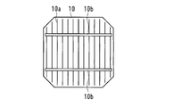
- the solar cell is provided with comb-like fingers 10 a and bus bars 10 b on the front and back surfaces of the photoelectric conversion unit 10.
- the finger 10a and the bus bar 10b are used as collector electrodes that extract the electric power generated by the photoelectric conversion unit 10 to the outside of the solar cell.
- the fingers 10a and the bus bars 10b are formed by applying a conductive paste on the photoelectric conversion unit 10 using screen printing or the like.
- the front and back surfaces of the photoelectric conversion unit 10 are sealed with a sealing material via a filler.
- a sealing material By sealing with the sealing material in this way, the photoelectric conversion unit 10 can be isolated from the outside air, and deterioration due to intrusion of moisture or the like can be prevented.
- the solar cell includes a semiconductor layer as the photoelectric conversion unit 10, and the metal contained in the finger 10 a and the bus bar 10 b may be diffused into the semiconductor layer to reduce efficiency.
- a solar cell module generates power upon receiving light, and includes a solar cell provided with a collector electrode containing silver on a surface thereof, covers the collector electrode, and includes titanium or a compound thereof and a resin. And the collector is a solar cell module having no peak at wavelengths of 1500 to 1700 cm ⁇ 1 in Raman spectral scattering measurement.
- the solar cell module according to the present invention it is possible to suppress a decrease in efficiency due to diffusion of a metal contained in a collecting electrode such as a finger or a bus bar.
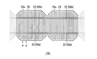
- the solar cell module 100 in the present embodiment includes a solar cell 20, a connecting member 22, a first filler 24, a first sealing material 26, a second filler 28, and a second filler.
- the sealing material 30 is included.
- FIG. 2 is a cross-sectional view taken along line AA in FIG. Note that the drawings referred to in the present embodiment are schematically described, and the ratios of the components drawn in the drawings may be different from actual ones. The dimensional ratios and the like may differ between drawings.
- the “light receiving surface” means a main surface on which sunlight mainly enters from the outside of the solar cell 20
- the “back surface” means a main surface opposite to the light receiving surface. For example, more than 50% to 100% of sunlight incident on the solar cell module 100 enters from the light receiving surface side.
- the solar cell 20 has a semiconductor junction such as a pn or pin junction, a crystalline semiconductor material such as single crystal Si or polycrystalline Si, a thin film semiconductor material such as an amorphous Si alloy or CuInSe, GaAs, It is comprised from semiconductor materials, such as compound semiconductor materials, such as InP. Further, an organic material such as a dye-sensitized type may be used.
- a semiconductor junction such as a pn or pin junction
- a crystalline semiconductor material such as single crystal Si or polycrystalline Si
- a thin film semiconductor material such as an amorphous Si alloy or CuInSe, GaAs
- semiconductor materials such as compound semiconductor materials, such as InP.
- an organic material such as a dye-sensitized type may be used.
- the solar cell 20 includes an i-type amorphous silicon layer, a p-type amorphous silicon layer, and a transparent conductive layer laminated on the light-receiving surface side of a crystalline semiconductor substrate, and an i-type amorphous silicon layer on the back side.
- the n-type amorphous silicon layer and the transparent conductive layer can be laminated.
- Such a solar cell including a configuration is called a HIT solar cell, and is an intrinsic (i-type) amorphous semiconductor between a crystalline semiconductor and a pn junction formed by a p-type amorphous semiconductor film. The conversion efficiency is drastically improved by inserting a film.
- the i-type amorphous silicon layer, the p-type amorphous silicon layer, the i-type amorphous silicon layer, and the p-type amorphous silicon layer are PECVD (Plasma Enhanced Chemical Vapor Deposition), Cat-CVD (Catalytic Chemical Vapor Deposition). ), A sputtering method or the like.
- PECVD any method such as RF plasma CVD, high-frequency VHF plasma CVD, or microwave plasma CVD may be used.
- an i-type amorphous silicon layer having a thickness of about 5 nm is formed on the light-receiving surface side of the substrate, and a p-type amorphous silicon layer having a thickness of about 5 nm is further formed. Further, an i-type amorphous silicon layer having a thickness of about 5 nm is formed on the back side of the substrate, and an n-type amorphous silicon layer having a thickness of about 20 nm is further formed.
- the transparent conductive layer includes, for example, at least one metal oxide such as indium oxide, zinc oxide, tin oxide, or titanium oxide, and tin, zinc, tungsten, antimony, titanium are included in these metal oxides. Further, a dopant such as cerium or gallium may be doped.
- the transparent conductive layer can be formed by a film formation method such as an evaporation method, a CVD method, or a sputtering method.
- the collector electrode for taking out the generated electric power outside is provided on the light receiving surface and the back surface of the solar cell 20.
- the collector electrode includes a finger 20a.
- the finger 20 a is an electrode for collecting carriers generated by the solar cell 20.
- the fingers 20a In order to collect carriers from the solar cell 20 as evenly as possible, the fingers 20a have a linear shape with a width of about 100 ⁇ m, for example, and are arranged every 2 mm.
- the bus bar 20b is a current collecting electrode for carriers collected by the plurality of fingers 20a.
- the bus bar 20b has a linear shape having a width of 1 mm, for example, and is arranged so as to intersect the fingers 20a along the direction in which the connection member 22 is arranged.
- the bus bar 20b is formed so as to be covered by the connection member 22. Moreover, it is good also as a structure which does not provide the bus-bar 20b.
- the installation area of the collector electrode provided on the light receiving surface side of the solar cell module 100 is smaller than that on the back surface side. That is, on the light receiving surface side of the solar cell module 100, the light shielding loss can be reduced by making the area that blocks the incident light as small as possible.
- a collecting electrode may be provided so as to cover the entire back surface of the solar cell module 100 instead of the finger 20a.
- the collector electrode can be formed using a conductive paste.
- a resin-type conductive paste using a resin material such as an epoxy resin as a binder and conductive particles such as silver particles as a filler can be used.
- the binder is mixed mainly for adhesion. In order to maintain reliability, the binder is required to be excellent in moisture resistance and heat resistance.
- the binder for example, at least one selected from an epoxy resin, an acrylic resin, a polyimide resin, a phenol resin, a urethane resin, a silicone resin, or a mixture or copolymerization of these resins may be applied.
- the filler is mixed for the purpose of obtaining the electrical conductivity of the collector electrode. Silver particles having different sizes may be mixed, or those having an uneven shape on the surface may be mixed.
- the solvent may be butyl carbitol acetate (BCA) or the like.
- the connection member 22 electrically connects the plurality of solar cells 20.
- the connecting member 22 can be, for example, a strip-shaped conductive ribbon.
- the collector electrodes of the solar cells 20 adjacent to each other are connected to each other in series or in parallel.
- the connection member 22 is bonded to the bus bar 20b, which is a collector electrode, by soldering or via a conductive paste or a conductive film. Thereby, the some solar cell 20 is connected in series or in parallel.
- the first sealing material 26 is disposed on the light receiving surface side of the solar cell module 100.
- the first sealing material 26 is a member that ensures the mechanical strength of the solar cell module 100.
- the 1st sealing material 26 is a member which has high rigidity.
- the 1st sealing material 26 can be comprised by a glass plate, a resin plate, etc. Especially, it is preferable that the 1st sealing material 26 is comprised with the glass plate.
- the glass plate has high rigidity and light transmittance, and is excellent in weather resistance.
- the first filler 24 is filled between the light receiving surface of the solar cell 20 and the first sealing material 26, and adheres the first sealing material 26 to the solar cell 20.
- the first filler 24 is preferably composed of a material that transmits light in a wavelength region used for photoelectric conversion in the solar cell 20.
- the first filler 24 preferably has an average light transmittance of 85% or more in a wavelength region of 400 nm to 1100 nm.
- the first filler 24 is at least one of ethylene / vinyl acetate copolymer (EVA), polyvinyl butyral (PVB), ethylene / vinyl alcohol copolymer, acrylic resin, polyethylene (PE), and polypropylene (PP). It is preferable to use a resin or a resin composition containing at least one of these resins.
- the second sealing material 30 is disposed on the back side of the solar cell module 100.
- the second sealing material 30 is disposed on the back surface of the solar cell module 100.
- the 2nd sealing material 30 can be comprised by the resin sheet etc. which consist of polyethylene terephthalate (PET) etc., for example.
- the inside of the resin sheet which comprises the 2nd sealing material 30 may be provided with metal foil, such as aluminum foil, an inorganic barrier layer with a low water permeability, etc., for example.
- the inorganic barrier layer can be formed of, for example, an inorganic oxide such as silicon oxide, aluminum oxide, or magnesium oxide.
- the second filler 28 is filled between the back surface of the solar cell 20 and the second sealing material 30 and adheres the second sealing material 30 to the solar cell 20.
- the second filler 28 is an ethylene / vinyl acetate copolymer (EVA), polyvinyl butyral (PVB), an ethylene / vinyl alcohol copolymer, an acrylic resin, polyethylene (PE), and polypropylene.
- the main component can be at least one resin of (PP) or a resin composition containing at least one resin of those resins.
- the second filler 28 preferably contains a colorant in addition to the resin.
- the colorant can be titanium oxide (TiO) particles.
- the titanium oxide particles are white.
- the first filler 24 and the second filler 28 are respectively applied to the light receiving surface side and the back surface side of the solar cells 20 connected in series and parallel by the connection member 22, and the first sealing material 26 and the second sealing material 30 are applied.
- the solar cell 20 is sealed by thermocompression bonding.
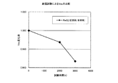
- FIG. 3 shows a solar cell module 100 (Example) in the present embodiment in which the second filler 28 contains titanium oxide, and a solar cell module using a filler not containing titanium oxide instead of the second filler 28.
- the change of the open circuit voltage (Voc) in a moisture resistance test with (comparative example) is shown.
- the comparative example was formed in the same manner as the solar cell module 100 except that a filler not containing titanium oxide was used instead of the second filler 28.
- the change in open circuit voltage (Voc) up to 3000 hours was measured in an environment of a temperature of 85 ° C. and a humidity of 85%.
- FIG. 3 shows the change after the start of the test with respect to the open circuit voltage ratio (the open circuit voltage of the comparative example / the open circuit voltage of the example) with the test start time being 1.
- the open circuit voltage ratio decreased as the test time increased from 2000 hours to 3000 hours. That is, in the solar cell module of the comparative example, the open circuit voltage (Voc) decreased as the test time increased from 2000 hours to 3000 hours, whereas the solar in this embodiment in which the second filler 28 contains titanium oxide. In the battery module 100, it can be said that the degree of decrease was very small compared to the comparative example.
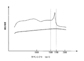
- FIG. 4 shows the Raman spectrum (solid line) of the surface of the solar cell module 100 and the collector electrode (finger 20a) in the comparative example. A similar Raman spectrum is obtained for the bus bar 20b.
- the Raman spectrum of the finger 20a was exposed by a microscopic laser Raman spectrometer (“inVia Reflex” manufactured by Renishaw) for 20 seconds in an extension mode as a laser beam having a wavelength of 785 nm as an excitation light source and a measurement mode.
- a microscopic laser Raman spectrometer (“inVia Reflex” manufactured by Renishaw) for 20 seconds in an extension mode as a laser beam having a wavelength of 785 nm as an excitation light source and a measurement mode.
- the peak appearing in the region of the wavelength of 1500 to 1700 cm ⁇ 1 of the Raman spectrum is more likely to appear as the binder ratio on the surface of the collector electrode (finger 20a) increases, and the Raman scattering intensity increases.
- the Raman scattering intensity increases as the ratio of exposure of the conductive filler (silver) to the surface of the collector electrode is reduced, the peak appearing in the wavelength region of 1500-1700 cm ⁇ 1 becomes larger and the Raman scattering intensity increases.
- a peak appears in the wavelength range of 1500 to 1700 cm ⁇ 1. Becomes apparent. This peak has a peak top wavelength of 1650 cm ⁇ 1 , and the peak top Raman scattering intensity is 10% or more higher than the scattering intensity Ik on the long wavelength side (1700 cm ⁇ 1 ) from the peak top wavelength by 50 cm ⁇ 1. ing.
- the conductive filler silver
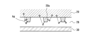
- the silver diffuses from the collector electrode to the second filler 28 as shown in FIG.
- Silver also diffuses into the 20.
- the moisture resistance test for the comparative example in which titanium oxide is not included in the filler it is considered that the diffusion of silver into the solar cell 20 progressed as the test time increased, and the open circuit voltage (Voc) decreased. .
- the diffusion of silver into the second filler 28 and further the diffusion of silver into the solar cell 20 is suppressed by titanium oxide. It is considered that the decrease of the open circuit voltage (Voc) was delayed.
- the solar cell 20 includes an amorphous silicon layer, the deterioration of characteristics due to the diffusion of silver into the amorphous silicon layer is greatly deteriorated, so that it is considered that the effect of suppressing the diffusion by titanium oxide becomes significant.
- the proportion of the conductive filler (silver) exposed on the surface of the collector electrode is increased, so that it is considered that the effect of suppressing diffusion by titanium oxide becomes significant.
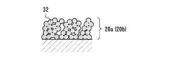
- a network structure 32 in which a large number of silver particles are fused to each other can be formed as shown in the schematic cross-sectional view of FIG.
- the network structure 32 can be confirmed as a structure in which more than half of the silver particles are fused and connected to each other in the microscopic observation of the collecting electrodes such as the fingers 20a and the bus bars 20b.
- the second filler 28 on the back surface side of the solar cell module 100 is configured to contain titanium oxide, but the first filler 24 may contain titanium oxide.
- the first filler 24 since the first filler 24 is provided on the light receiving surface side of the solar cell module 100, it is preferable that the first filler 24 be set to such a degree that the scattering loss of light incident on the solar cell module 100 is not significant.
- 10 photoelectric conversion part 10a finger, 10b bus bar, 20 solar cell, 20a finger, 20b bus bar, 22 connecting member, 24 first filler, 26 first sealing material, 28 second filling material, 30 second sealing material 32 network structure, 100 solar cell modules.
Landscapes
- Photovoltaic Devices (AREA)
Description
本発明は、太陽電池モジュールに関する。
太陽電池は、図8に示すように、光電変換部10の表面及び裏面に櫛状のフィンガー10a及びバスバー10bが設けられている。フィンガー10a及びバスバー10bは、光電変換部10で発電された電力を太陽電池の外部へ取り出す集電極として利用される。フィンガー10a及びバスバー10bは、スクリーン印刷等を用いて導電性ペーストを光電変換部10上に塗布することによって形成される。
また、光電変換部10の表裏面は、充填材を介して封止材によって封止される。このように封止材によって封止することによって、光電変換部10を外気から隔離し、水分等の浸入による劣化を防ぐことができる。
また、太陽電池の裏面側に間に位置している充填材を着色する技術が開示されている(特許文献1参照)。このように、充填材を着色することによって、光電変換部10を透過してきた光が散乱しやすくなり、太陽電池の光電変換効率をより高めることができる。
ところで、太陽電池では光電変換部10として半導体層を含み、フィンガー10aやバスバー10bに含まれる金属がこの半導体層に拡散することによって効率が低下するおそれがある。
本発明に係る太陽電池モジュールの一態様は、光の入射を受けて発電を行い、表面に銀を含む集電極が設けられた太陽電池と、集電極を覆い、チタン又はその化合物及び樹脂を含む充填材と、を備え、集電極は、ラマン分光散乱測定において波長1500~1700cm-1にピークを持たない、太陽電池モジュールである。
本発明に係る太陽電池モジュールによれば、フィンガーやバスバー等の集電極に含まれる金属の拡散による効率低下を抑制することができる。
本実施の形態における太陽電池モジュール100は、図1及び図2に示すように、太陽電池20、接続部材22、第1充填材24、第1封止材26、第2充填材28及び第2封止材30を含んで構成される。
図2は、図1のラインA-Aに沿った断面図である。なお、本実施の形態で参照する図面は模式的に記載されたものであり、図面に描画された構成の比率などは、現実とは異なる場合がある。図面相互においても、寸法比率等が異なる場合がある。
また、「受光面」とは太陽電池20の外部から太陽光が主に入射する主面を、「裏面」とは受光面と反対側の主面をそれぞれ意味する。例えば、太陽電池モジュール100に入射する太陽光のうち50%超過~100%が受光面側から入射する。
太陽電池20は、pn或いはpin接合等の半導体接合を有しており、単結晶Si、多結晶Si等の結晶系半導体材料、非晶質Si系合金或いはCuInSe等の薄膜半導体材料、或いはGaAs、InP等の化合物半導体材料等の半導体材料から構成されている。また、色素増感型等の有機材料を用いてもよい。
例えば、太陽電池20は、結晶系半導体の基板の受光面側にi型非晶質シリコン層及びp型非晶質シリコン層及び透明導電層を積層し、裏面側にi型非晶質シリコン層、n型非晶質シリコン層及び透明導電層を積層して構成することができる。このような、構成を含む太陽電池は、HIT太陽電池と呼ばれるものであり、結晶系半導体とp型非晶質半導体膜で形成されるpn接合の間に真性(i型)の非晶質半導体膜を介挿することによって変換効率を飛躍的に向上させたものである。
i型非晶質シリコン層、p型非晶質シリコン層、i型非晶質シリコン層及びp型非晶質シリコン層は、PECVD(Plasma Enhansed Chemical Vapor Deposition)、Cat-CVD(Catalytic Chemical Vapor Deposition)、スパッタリング法等により形成することができる。PECVDは、RFプラズマCVD法、周波数の高いVHFプラズマCVD法、さらにはマイクロ波プラズマCVD法などいずれの手法を用いてもよい。例えば、基板の受光面側に約5nmの厚みを有するi型非晶質シリコン層を形成し、さらに約5nmの厚みを有するp型非晶質シリコン層を形成する。また、基板の裏面側に約5nmの厚みを有するi型非晶質シリコン層を形成し、さらに約20nmの厚みを有するn型非晶質シリコン層を形成する。
透明導電層は、例えば、酸化インジウム、酸化亜鉛、酸化錫、または酸化チタンなどの金属酸化物を少なくとも一つを含んで構成され、これらの金属酸化物に、錫、亜鉛、タングステン、アンチモン、チタン、セリウム、ガリウムなどのドーパントがドープされていてもよい。透明導電層は、蒸着法、CVD法、スパッタリング法等の成膜方法により形成することができる。
太陽電池20の受光面及び裏面には、発電された電力を外部に取り出すための集電極が設けられる。集電極は、フィンガー20aを含む。フィンガー20aは、太陽電池20で生成されたキャリアの収集用の電極である。フィンガー20aは、太陽電池20からできるだけ均等にキャリアを収集するために、例えば100μm程度の幅を有する線形状とされ、2mmおきに配置される。さらに、フィンガー20aを接続するバスバー20bを設けてもよい。バスバー20bは、複数のフィンガー20aで収集されたキャリアの集電用電極である。バスバー20bは、例えば1mmの幅を有する線形状とされ、接続部材22が配置される方向に沿ってフィンガー20aと交差するように配置される。フィンガー20a及びバスバー20bの本数や面積は、太陽電池モジュール100の大きさや抵抗を考慮して適宜に設定される。なお、本実施の形態では、バスバー20bは接続部材22に覆われるように形成されている。また、バスバー20bを設けない構成としてもよい。
なお、太陽電池モジュール100の受光面側に設けられる集電極の設置面積は裏面側よりも小さくすることが好ましい。すなわち、太陽電池モジュール100の受光面側では、入射光を遮る面積をできるだけ小さくすることによって遮光ロスを低減することができる。一方、裏面側では入射光を考慮する必要がなく、フィンガー20aの代りに太陽電池モジュール100の裏面全面を覆うように集電極を設けてもよい。
また、集電極は、導電性ペーストを用いて形成することができる。導電性ペーストとして、例えば、エポキシ樹脂等の樹脂材料をバインダとし、銀粒子等の導電性粒子をフィラーとした樹脂型導電性ペーストを用いることができる。バインダは、接着を主目的として混合される。信頼性を維持するためには、バインダは、耐湿性や耐熱性に優れていることが要求される。バインダは、例えば、エポキシ樹脂、アクリル樹脂、ポリイミド樹脂、フェノール樹脂、ウレタン樹脂、シリコーン樹脂等から選ばれる少なくとも一種、あるいは、これらの樹脂の混合、共重合などを適用すればよい。フィラーは、集電極の電気伝導性を得ることを目的に混入される。銀粒子は、サイズの異なるものを混合したり、表面に凹凸形状を設けたものを混合したりしてもよい。また、必要に応じて、導電性ペーストに溶剤を加えてもよい。溶剤は、ブチルカルビトールアセテート(BCA)等とすればよい。
接続部材22は、複数の太陽電池20を電気的に接続する。接続部材22は、例えば、短冊状の導電性リボンとすることができる。部材隣り合う太陽電池20の集電極を相互に直列又は並列に接続する。接続部材22は、集電極であるバスバー20bにハンダ付け又は導電性ペーストや導電性フィルムを介して接着される。これにより、複数の太陽電池20が直列又は並列接続される。
第1封止材26は、太陽電池モジュール100の受光面側に配される。第1封止材26は、太陽電池モジュール100の機械的強度を担保する部材である。このため、第1封止材26は、高い剛性を有する部材であることが好ましい。第1封止材26は、ガラス板や樹脂板などにより構成することができる。なかでも、第1封止材26は、ガラス板により構成されていることが好ましい。ガラス板は、剛性及び光透過率が高く、かつ耐候性に優れている。
第1充填材24は、太陽電池20の受光面と第1封止材26との間に充填され、第1封止材26を太陽電池20に接着する。第1充填材24は、太陽電池20における光電変換に使用される波長域の光を透過させる材料から構成することが好ましい。例えば、太陽電池20にシリコン材料を使用した場合、第1充填材24は、400nm~1100nmの波長域における平均光透過率が85%以上のものであることが好ましい。第1充填材24は、エチレン・酢酸ビニル共重合体(EVA)、ポリビニルブチラール(PVB)、エチレン・ビニルアルコール共重合体、アクリル樹脂、ポリエチレン(PE)及びポリプロピレン(PP)のうちの少なくとも一種の樹脂や、それらの樹脂のうちの少なくとも一種の樹脂を含む樹脂組成物とすることが好適である。
第2封止材30は、太陽電池モジュール100の裏面側に配される。第2封止材30は、太陽電池モジュール100の裏面に配される。第2封止材30は、例えば、ポリエチレンテレフタレート(PET)などからなる樹脂シートなどにより構成することができる。なお、第2封止材30を構成する樹脂シートの内部には、例えば、アルミニウム箔などの金属箔や、水分透過性が低い無機バリア層等が設けられていてもよい。無機バリア層は、例えば、酸化珪素、酸化アルミニウム、酸化マグネシウム等の無機酸化物などにより形成することができる。
第2充填材28は、太陽電池20の裏面と第2封止材30との間に充填され、第2封止材30を太陽電池20に接着する。第2充填材28は、第1充填材24と同様に、エチレン・酢酸ビニル共重合体(EVA)、ポリビニルブチラール(PVB)、エチレン・ビニルアルコール共重合体、アクリル樹脂、ポリエチレン(PE)及びポリプロピレン(PP)のうちの少なくとも一種の樹脂や、それらの樹脂のうちの少なくとも一種の樹脂を含む樹脂組成物を主成分とすることができる。
ここで、第2充填材28は、上記樹脂に加えて着色剤を含むことが好ましい。着色剤は、酸化チタン(TiO)粒子とすることができる。酸化チタン粒子は白色であり、酸化チタン粒子を第2充填材28に混入させることにより、第2充填材28において光が散乱しやすくなり、太陽電池モジュール100の光電変換効率をより高めることができる。
接続部材22によって直並列接続された太陽電池20の受光面側及び裏面側に第1充填材24及び第2充填材28をそれぞれ塗布し、第1封止材26及び第2封止材30を加熱圧着することによって太陽電池20は封止される。
図3は、第2充填材28に酸化チタンを含む本実施の形態における太陽電池モジュール100(実施例)と、第2充填材28の代りに酸化チタンを含まない充填材を用いた太陽電池モジュール(比較例)との耐湿試験における開放電圧(Voc)の変化を示す。ここで、比較例は、第2充填材28の代りに酸化チタンを含まない充填材を用いた点を除いて太陽電池モジュール100と同様に形成した。また、耐湿試験では、温度85℃及び湿度85%の環境下において3000時間までの開放電圧(Voc)の変化を測定した。図3では、開放電圧比(比較例の開放電圧/実施例の開放電圧)について、試験開始時を1として、試験開始後の変化を示した。
図3に示されるように、試験時間が2000時間から3000時間と増加するにつれて開放電圧比が低下した。すなわち、比較例の太陽電池モジュールでは試験時間が2000時間から3000時間と増加するにつれて開放電圧(Voc)が低下したのに対して、第2充填材28に酸化チタンを含む本実施の形態における太陽電池モジュール100では比較例に比べて低下の度合いは非常に小さかったといえる。
図4は、太陽電池モジュール100及び比較例における集電極(フィンガー20a)の表面のラマンスペクトル(実線)を示す。なお、バスバー20bについても同様のラマンスペクトルが得られる。
図4の実線に示すように、フィンガー20aの表面のラマンスペクトルが波長1500~1700cm-1にピークを有さない場合に開放電圧(Voc)の低減の抑制効果が顕著となる。なお、本実施の形態では、ピークトップにおける散乱強度(シグナル強度とも呼ばれる)が、ピークトップの波長から50cm-1長波長側における散乱強度よりも10%以上高い場合にピークが存在するものとする。フィンガー20aのラマンスペクトルは、顕微レーザーラマン分光装置(レニショー社製「inVia Reflex」)によって、励起光源として波長785nmのレーザー光及び測定モードとしてExtentionモードにて20秒露光して行った。
ラマンスペクトルの波長1500~1700cm-1の領域に現われるピークは、集電極(フィンガー20a)の表面におけるバインダの割合が多くなるほど出現し易くなり、ラマン散乱強度が高くなる。換言すると、集電極の表面に導電性フィラー(銀)が露出する割合を減らすほど、波長1500~1700cm-1の領域に現われるピークが大きくなり、ラマン散乱強度が高くなる。
例えば、集電極の総重量に対する銀粒子の含有量を80~85重量%とした導電性ペーストを用いて形成した場合、図4の破線に示すように、波長1500~1700cm-1の領域にピークが顕在化する。このピークは、ピークトップの波長が1650cm-1にあり、ピークトップのラマン散乱強度が、ピークトップの波長から50cm-1長波長側(1700cm-1)における散乱強度Ikよりも10%以上高くなっている。
一方、本実施の形態の太陽電池モジュール100では、波長1500~1700cm-1の領域にはピークがみられなかった。これは、集電極に含まれる導電性フィラー(銀)の割合が高く、集電極の表面に露出した導電性フィラー(銀)の割合が大きく、バインダの露出が少ないためと考えられる。
集電極の表面への導電性フィラー(銀)の露出が大きい場合、図5に示すように、集電極から第2充填材28へ銀が拡散し、さらに第2充填材28を介して太陽電池20内にも銀が拡散する。充填材に酸化チタンが含まれない比較例に対する耐湿試験では、試験時間の増加に伴って太陽電池20内への銀の拡散が進行し、開放電圧(Voc)の低下が生じたものと考えられる。
一方、本実施の形態における太陽電池モジュール100に対する耐湿試験では、図6に示すように、第2充填材28への銀の拡散、さらには太陽電池20内への銀の拡散が酸化チタンによって抑制され、開放電圧(Voc)の低下が遅らせられたものと考えられる。特に、太陽電池20に非晶質シリコン層が含まれる場合、非晶質シリコン層に対する銀の拡散による特性の劣化が大きいので、酸化チタンによる拡散抑制の効果が顕著となると考えられる。
さらに、集電極に含まれる銀粒子がネットワーク構造を有する場合、集電極の表面に露出した導電性フィラー(銀)の割合が大きくなるため、酸化チタンによる拡散抑制の効果が顕著となると考えられる。集電極の形成時において銀粒子の特性や加熱温度を調整することによって、図7の断面模式図に示すように、多数の銀粒子が相互に融着したネットワーク構造32を形成することができる。ネットワーク構造32は、フィンガー20aやバスバー20b等の集電極の顕微鏡観察において銀粒子の半分以上が融着して互いに繋がり合った構造として確認することができる。
なお、本実施の形態では、太陽電池モジュール100の裏面側の第2充填材28に酸化チタンを含有させる構成としたが、第1充填材24に酸化チタンを含有させてもよい。ただし、第1充填材24は太陽電池モジュール100の受光面側に設けられるので、太陽電池モジュール100に入射される光の散乱ロスが顕著とならない程度とすることが好ましい。
10 光電変換部、10a フィンガー、10b バスバー、20 太陽電池、20a フィンガー、20b バスバー、22 接続部材、24 第1充填材、26 第1封止材、28 第2充填材、30 第2封止材、32 ネットワーク構造、100 太陽電池モジュール。
Claims (4)
- 光の入射を受けて発電を行い、表面に銀を含む集電極が設けられた太陽電池と、
前記集電極を覆い、チタン又はその化合物及び樹脂を含む充填材と、
を備え、
前記集電極は、ラマン分光散乱測定において波長1500~1700cm-1にピークを持たない、太陽電池モジュール。 - 請求項1に記載の太陽電池モジュールであって、
前記集電極は、銀粒子が相互に融着されたネットワーク構造を有する、太陽電池モジュール。 - 請求項1又は2に記載の太陽電池モジュールであって、
前記太陽電池は、結晶系シリコン層と、前記結晶系シリコン層上に形成された非晶質シリコン層と、の積層構造を有する、太陽電池モジュール。 - 請求項3に記載の太陽電池モジュールであって、
前太陽電池は、前記非晶質シリコン層上に形成された透明導電膜を有する、太陽電池モジュール。
Priority Applications (2)
| Application Number | Priority Date | Filing Date | Title |
|---|---|---|---|
| JP2014526692A JPWO2014016962A1 (ja) | 2012-07-27 | 2012-07-27 | 太陽電池モジュール |
| PCT/JP2012/069207 WO2014016962A1 (ja) | 2012-07-27 | 2012-07-27 | 太陽電池モジュール |
Applications Claiming Priority (1)
| Application Number | Priority Date | Filing Date | Title |
|---|---|---|---|
| PCT/JP2012/069207 WO2014016962A1 (ja) | 2012-07-27 | 2012-07-27 | 太陽電池モジュール |
Publications (1)
| Publication Number | Publication Date |
|---|---|
| WO2014016962A1 true WO2014016962A1 (ja) | 2014-01-30 |
Family
ID=49996795
Family Applications (1)
| Application Number | Title | Priority Date | Filing Date |
|---|---|---|---|
| PCT/JP2012/069207 Ceased WO2014016962A1 (ja) | 2012-07-27 | 2012-07-27 | 太陽電池モジュール |
Country Status (2)
| Country | Link |
|---|---|
| JP (1) | JPWO2014016962A1 (ja) |
| WO (1) | WO2014016962A1 (ja) |
Citations (3)
| Publication number | Priority date | Publication date | Assignee | Title |
|---|---|---|---|---|
| JP2005216963A (ja) * | 2004-01-27 | 2005-08-11 | Kyocera Corp | 太陽電池モジュール |
| JP2005276939A (ja) * | 2004-03-23 | 2005-10-06 | Sanyo Electric Co Ltd | 光起電力装置 |
| JP2007224191A (ja) * | 2006-02-24 | 2007-09-06 | Sanyo Electric Co Ltd | 導電性ペースト組成物及びそのペースト組成物を用いた太陽電池セル、並びにそのセルを用いた太陽電池モジュール |
Family Cites Families (3)
| Publication number | Priority date | Publication date | Assignee | Title |
|---|---|---|---|---|
| JP2975222B2 (ja) * | 1992-11-17 | 1999-11-10 | キヤノン株式会社 | 太陽電池封止用樹脂組成物 |
| JP2011069653A (ja) * | 2009-09-24 | 2011-04-07 | Panasonic Electric Works Co Ltd | エポキシ樹脂含有材料の硬化度評価方法 |
| JP2011258879A (ja) * | 2010-06-11 | 2011-12-22 | Toyo Ink Sc Holdings Co Ltd | 太陽電池モジュール |
-
2012
- 2012-07-27 JP JP2014526692A patent/JPWO2014016962A1/ja active Pending
- 2012-07-27 WO PCT/JP2012/069207 patent/WO2014016962A1/ja not_active Ceased
Patent Citations (3)
| Publication number | Priority date | Publication date | Assignee | Title |
|---|---|---|---|---|
| JP2005216963A (ja) * | 2004-01-27 | 2005-08-11 | Kyocera Corp | 太陽電池モジュール |
| JP2005276939A (ja) * | 2004-03-23 | 2005-10-06 | Sanyo Electric Co Ltd | 光起電力装置 |
| JP2007224191A (ja) * | 2006-02-24 | 2007-09-06 | Sanyo Electric Co Ltd | 導電性ペースト組成物及びそのペースト組成物を用いた太陽電池セル、並びにそのセルを用いた太陽電池モジュール |
Also Published As
| Publication number | Publication date |
|---|---|
| JPWO2014016962A1 (ja) | 2016-07-07 |
Similar Documents
| Publication | Publication Date | Title |
|---|---|---|
| JP6688230B2 (ja) | 太陽電池およびその製造方法、ならびに太陽電池モジュール | |
| JP2010041012A (ja) | 太陽電池モジュール | |
| JP5642355B2 (ja) | 太陽電池モジュール | |
| WO2013002102A1 (ja) | 光電変換装置 | |
| JP5995204B2 (ja) | 光電変換素子 | |
| JP2017139267A (ja) | 太陽電池素子および太陽電池モジュール | |
| JP5554409B2 (ja) | 光電変換装置 | |
| US20120118358A1 (en) | Solar cell module | |
| JP2019079916A (ja) | バックコンタクト型太陽電池モジュール | |
| KR20140095658A (ko) | 태양 전지 | |
| KR20110045246A (ko) | 태양 전지 셀 및 이를 구비한 태양 전지 모듈 | |
| WO2013031199A1 (ja) | 太陽電池モジュール | |
| KR101694553B1 (ko) | 태양 전지 모듈 | |
| TWI596791B (zh) | 太陽能電池模組 | |
| JP5968244B2 (ja) | 光電変換モジュールおよびその製造方法 | |
| JP2015138829A (ja) | 太陽電池モジュール | |
| US9059357B2 (en) | Bifacial solar cell | |
| JP2016225362A (ja) | 太陽電池素子、太陽電池モジュールおよび太陽電池素子の製造方法 | |
| JPWO2014016954A1 (ja) | 太陽電池 | |
| JPWO2014016962A1 (ja) | 太陽電池モジュール | |
| WO2012105153A1 (ja) | 光電変換素子 | |
| JP4911878B2 (ja) | 半導体/電極のコンタクト構造とこれを用いた半導体素子、太陽電池素子、並びに太陽電池モジュール | |
| US20110308569A1 (en) | Multi-terminal solar panel | |
| JP6192562B2 (ja) | 太陽電池素子および太陽電池モジュール | |
| WO2015045263A1 (ja) | 太陽電池及び太陽電池モジュール |
Legal Events
| Date | Code | Title | Description |
|---|---|---|---|
| 121 | Ep: the epo has been informed by wipo that ep was designated in this application |
Ref document number: 12881797 Country of ref document: EP Kind code of ref document: A1 |
|
| ENP | Entry into the national phase |
Ref document number: 2014526692 Country of ref document: JP Kind code of ref document: A |
|
| NENP | Non-entry into the national phase |
Ref country code: DE |
|
| 122 | Ep: pct application non-entry in european phase |
Ref document number: 12881797 Country of ref document: EP Kind code of ref document: A1 |