WO2014010211A1 - 発光モジュール - Google Patents
発光モジュール Download PDFInfo
- Publication number
- WO2014010211A1 WO2014010211A1 PCT/JP2013/004178 JP2013004178W WO2014010211A1 WO 2014010211 A1 WO2014010211 A1 WO 2014010211A1 JP 2013004178 W JP2013004178 W JP 2013004178W WO 2014010211 A1 WO2014010211 A1 WO 2014010211A1
- Authority
- WO
- WIPO (PCT)
- Prior art keywords
- phosphor
- light emitting
- conversion layer
- wavelength conversion
- light
- Prior art date
- Legal status (The legal status is an assumption and is not a legal conclusion. Google has not performed a legal analysis and makes no representation as to the accuracy of the status listed.)
- Ceased
Links
Images








Classifications
-
- H—ELECTRICITY
- H10—SEMICONDUCTOR DEVICES; ELECTRIC SOLID-STATE DEVICES NOT OTHERWISE PROVIDED FOR
- H10H—INORGANIC LIGHT-EMITTING SEMICONDUCTOR DEVICES HAVING POTENTIAL BARRIERS
- H10H20/00—Individual inorganic light-emitting semiconductor devices having potential barriers, e.g. light-emitting diodes [LED]
- H10H20/80—Constructional details
- H10H20/85—Packages
- H10H20/851—Wavelength conversion means
- H10H20/8511—Wavelength conversion means characterised by their material, e.g. binder
- H10H20/8512—Wavelength conversion materials
- H10H20/8513—Wavelength conversion materials having two or more wavelength conversion materials
-
- H—ELECTRICITY
- H10—SEMICONDUCTOR DEVICES; ELECTRIC SOLID-STATE DEVICES NOT OTHERWISE PROVIDED FOR
- H10H—INORGANIC LIGHT-EMITTING SEMICONDUCTOR DEVICES HAVING POTENTIAL BARRIERS
- H10H20/00—Individual inorganic light-emitting semiconductor devices having potential barriers, e.g. light-emitting diodes [LED]
- H10H20/80—Constructional details
- H10H20/85—Packages
- H10H20/852—Encapsulations
- H10H20/854—Encapsulations characterised by their material, e.g. epoxy or silicone resins
-
- H—ELECTRICITY
- H10—SEMICONDUCTOR DEVICES; ELECTRIC SOLID-STATE DEVICES NOT OTHERWISE PROVIDED FOR
- H10W—GENERIC PACKAGES, INTERCONNECTIONS, CONNECTORS OR OTHER CONSTRUCTIONAL DETAILS OF DEVICES COVERED BY CLASS H10
- H10W72/00—Interconnections or connectors in packages
- H10W72/851—Dispositions of multiple connectors or interconnections
- H10W72/874—On different surfaces
- H10W72/877—Bump connectors and die-attach connectors
-
- H—ELECTRICITY
- H10—SEMICONDUCTOR DEVICES; ELECTRIC SOLID-STATE DEVICES NOT OTHERWISE PROVIDED FOR
- H10W—GENERIC PACKAGES, INTERCONNECTIONS, CONNECTORS OR OTHER CONSTRUCTIONAL DETAILS OF DEVICES COVERED BY CLASS H10
- H10W90/00—Package configurations
- H10W90/701—Package configurations characterised by the relative positions of pads or connectors relative to package parts
- H10W90/721—Package configurations characterised by the relative positions of pads or connectors relative to package parts of bump connectors
- H10W90/724—Package configurations characterised by the relative positions of pads or connectors relative to package parts of bump connectors between a chip and a stacked insulating package substrate, interposer or RDL
Definitions
- the present invention relates to a light emitting module.
- LEDs light-emitting diodes
- a technique for obtaining a light-emitting module that emits light of a color different from the color of light emitted from the light-emitting element by converting the wavelength of light emitted from the light-emitting element such as an LED using a phosphor or the like are known.
- a technique has been proposed in which, for example, a ceramic layer including a wavelength conversion material is disposed in the path of light emitted by the light emitting layer (for example, , See Patent Document 1).
- the present invention has been made in view of such a situation, and an object thereof is to provide a technology capable of realizing a highly efficient light emitting module.
- a light emitting module includes a light emitting element that emits ultraviolet light or short wavelength visible light, and a first phosphor that emits blue light when excited by ultraviolet light or short wavelength visible light. And a second wavelength conversion layer having a second phosphor that is excited by ultraviolet light or short-wavelength visible light and emits yellow light.
- the first wavelength conversion layer and the second wavelength conversion layer are laminated on the light emitting surface of the light emitting element, and at least one of the first wavelength conversion layer and the second wavelength conversion layer is a ceramic layer.
- the second phosphor has a maximum excitation spectrum intensity of Imax in a wavelength region of 300 nm or more, Ia, and the excitation spectrum intensity at the peak wavelength of ultraviolet light or short-wavelength visible light emitted from the light emitting element is Ia. Imax ⁇ Ia is satisfied.
- the second phosphor since the second phosphor has high excitation spectrum intensity at the peak wavelength of ultraviolet light or short-wavelength visible light emitted from the light-emitting element, the light from the light-emitting element can be efficiently converted into yellow light.
- the first wavelength conversion layer may be disposed between the light emitting element and the second wavelength conversion layer, and the second wavelength conversion layer may be a ceramic layer.
- the second phosphor When the maximum intensity of the excitation spectrum in the wavelength region of 300 nm or more is Imax and the intensity of the excitation spectrum at the peak wavelength of visible light emitted from the first phosphor is Ib, the second phosphor has Ib ⁇ 0.8 ⁇ Imax. Meet. Thereby, in the 2nd fluorescent substance, absorption of the light which a 1st fluorescent substance emits can be suppressed.
- the first wavelength conversion layer is configured by dispersing the first phosphor in a transparent sealing material, and may have a thickness of 15 to 1000 ⁇ m.
- the first wavelength conversion layer may contain 0.5 to 35% by volume of the first phosphor. Thereby, the light of the light emitting element which passes through the first wavelength conversion layer and reaches the second wavelength conversion layer can be increased.
- the thickness of the second wavelength conversion layer may be 30 to 1000 ⁇ m.
- a highly efficient light emitting module can be realized.
- FIG. 1 is a cross-sectional view illustrating a schematic structure of a light emitting module according to Example 1.
- FIG. It is sectional drawing which shows schematic structure of the light emitting module which concerns on a comparative example. It is a figure which shows the measurement result of the transmittance
- FIG. 6 is a cross-sectional view illustrating a schematic structure of a light emitting module according to Example 2.
- FIG. It is a figure which shows the emission spectrum of the light emitting module which concerns on Example 2 and Comparative Example 1.
- FIG. 6 is a cross-sectional view illustrating a schematic structure of a light emitting module according to Example 3.
- FIG. It is sectional drawing which shows schematic structure of the light emitting module which concerns on the comparative example 2.
- FIG. It is a figure which shows the measurement result of the transmittance
- FIG. 6 is a cross-sectional view illustrating a schematic structure of a light emitting module according to Example 4.
- FIG. It is sectional drawing which shows schematic structure of the light emitting module which concerns on the comparative example 3.
- FIG. It is a figure which shows the emission spectrum of the light emitting module which concerns on Example 4 and Comparative Example 3.
- FIG. 2 is a diagram showing an emission spectrum of the semiconductor light emitting device according to Example 1.
- a white LED module combines a semiconductor light emitting element that emits light having a wavelength from near ultraviolet to blue with a phosphor that converts light emitted from the semiconductor light emitting element into visible light having a longer wavelength than that light. Is realized.
- Examples of white LED modules include a blue LED chip and a YAG (Yttrium Aluminum Garnet) phosphor that emits yellow light, a blue LED chip and two types of fluorescent light that emit red and green, respectively.
- a blue LED chip and a YAG (Yttrium Aluminum Garnet) phosphor that emits yellow light
- a blue LED chip and two types of fluorescent light that emit red and green, respectively.
- a phosphor layer in an LED module when a powdered phosphor is dispersed in a transparent sealing material (organic resin material, inorganic amorphous material, inorganic sol-gel material), the powdered phosphor acts as a filler. To do. Therefore, light loss occurs before the light emitted from the LED chip is extracted to the outside, which may be a cause of reducing the light emission efficiency of the light emitting module. This is due to the difference in refractive index between the phosphor and the sealing material, and this difference in refractive index causes scattering and reflection, resulting in light loss.
- the phosphor layer is formed of a phosphor single component, there is no interface between the phosphor and other components in the layer, there is no difference in refractive index, and the above-mentioned light loss is greatly increased. To be reduced. As a result, the luminous efficiency of the LED module can be increased as compared with a case where a powdered phosphor is dispersed in a transparent resin to form a phosphor layer.
- YAG is the only phosphor that has been successfully made into translucent ceramics while maintaining high quantum efficiency.
- the blue LED has higher directivity of light emission than the translucent ceramic YAG, so that the colors are separated.
- a technique of adding a scatterer component to the translucent ceramics YAG is effective, but on the other hand, the transmittance of the ceramics YAG is lowered and a sufficient luminous flux cannot be obtained.
- such a white LED module is suitable for realizing white light having a high color temperature of about daylight white, but it is difficult to form light of low color temperature such as warm white and light bulb color. And in order to form light of these low color temperatures, it is common to mix phosphors that absorb blue light and emit red light, but a red ring is easily formed on the outer periphery of the light emitting surface, It tends to lead to color separation.
- the light emitting module absorbs ultraviolet light and short wavelength visible light, and a semiconductor light emitting element such as an LED chip that emits ultraviolet light and short wavelength visible light (for example, visible light having a wavelength from purple to near ultraviolet).
- a semiconductor light emitting element such as an LED chip that emits ultraviolet light and short wavelength visible light (for example, visible light having a wavelength from purple to near ultraviolet).
- a phosphor layer having a phosphor that emits light, and the phosphor layer may be a ceramic layer densely sintered with a phosphor single component. Moreover, it is preferable that a ceramic layer has translucency.
- the phosphor may be of one type or a plurality of types as long as a desired emission color can be obtained as a light emitting module.
- At least one kind of phosphor layer may be a ceramic layer.
- a phosphor layer having a shape in which the powder phosphor is sealed with a transparent sealing material organic resin material, inorganic amorphous material, inorganic sol-gel material
- a transparent sealing material organic resin material, inorganic amorphous material, inorganic sol-gel material
- the phosphor layer that emits light with the highest visibility is arranged on the uppermost layer (light extraction surface side).
- the translucent ceramic phosphor is characterized by its high spectral transmittance, and has a transmittance (when measured in air) of 70 to 85%, preferably 80% in the wavelength range of 350 to 900 nm including the visible light region. That's it. However, this is not the case in the absorption band of the phosphor itself (wavelength range of the excitation band).
- the theoretical maximum transmittance (measured in air) is uniquely determined by the refractive index of the phosphor itself.
- the transmittance only in the phosphor medium is 80 to 100%, preferably 90% or more. However, this is not the case in the absorption band of the phosphor itself (wavelength range of the excitation band).
- the translucent ceramic phosphor when the translucent ceramic phosphor is mounted on the light emitting module, the phosphor layer is processed to have a thickness of 40 to 2000 ⁇ m, and preferably 80 to 2000 ⁇ m considering workability.
- the surface of the translucent ceramic phosphor is roughened and patterned by various processes such as Fresnel lens processing, V-groove processing, laser processing, nanoprinting processing, ion milling, and sandblasting.
- a white transparent material such as resin or glass having an arbitrary refractive index may be applied and formed into a film.
- the translucent ceramic phosphor is excellent in workability
- the light extraction direction and orientation can be controlled by, for example, prism shape processing, lens shape processing, various step processing, and vapor deposition of reflectors.
- these shape control can also give a desired shape without said process by shape
- mirror polishing and the total reflection effect that accompanies it it is possible to dimm only a predetermined part, guide the light, control the light extraction part, and the like.
- the transmittance of the phosphor layer having a shape in which the powdered phosphor is sealed with a transparent sealing material (organic resin material, inorganic amorphous material, inorganic sol-gel material) or the like is the transmittance of the translucent ceramic phosphor.
- a sealed phosphor layer may be used, and the manufacturing cost can be reduced.
- the spectral transmittance of the sealed phosphor layer is in the range of 60 to 85% (measured in air) in the wavelength range of 350 to 900 nm including the visible light range, preferably 65% or more. is there.
- a fine particle raw material of the phosphor is prepared, and an appropriate sintering aid is added as necessary. Thereafter, the phosphor fine particle material is molded by uniaxial pressure molding, CIP molding (cold one pressure molding) or the like. Or it mixes with resin, such as PVA (polyvinyl alcohol) and PVB (polyvinyl butyral), is made into a slurry, and shape
- resin such as PVA (polyvinyl alcohol) and PVB (polyvinyl butyral
- a light emitting module includes a light emitting element that emits ultraviolet light or short wavelength visible light, and a first phosphor that emits blue light when excited by ultraviolet light or short wavelength visible light. And a second wavelength conversion layer having a second phosphor that is excited by ultraviolet light or short-wavelength visible light and emits yellow light.
- the first wavelength conversion layer and the second wavelength conversion layer are laminated on the light emitting surface of the light emitting element, and at least one of the first wavelength conversion layer and the second wavelength conversion layer is a ceramic layer. is there.
- an LED is described as an example of a light emitting element, but a laser diode (LD) element, an electroluminescence (EL) element, or the like can also be used.
- the light emitting element preferably emits ultraviolet light or short wavelength visible light having a peak wavelength in the wavelength range of 350 to 420 nm.
- white light is realizable using several types of fluorescent substance from which an emission spectrum differs, for example, the blue fluorescent substance and yellow fluorescent substance which concern on each Example.
- white light can be realized by mixing blue light and yellow light without directly using light from the light emitting element.
- the transmittance of the phosphor layer is improved and the scattering loss is greatly reduced, so that the efficiency of the light emitting module can be improved.
- a white LED module as a light emitting module includes an LED chip that emits near ultraviolet light, a first phosphor (phosphor 1) that absorbs near ultraviolet light and emits blue light, and absorbs near ultraviolet light. And a second phosphor that emits yellow light (phosphor 2).
- a novel white LED module can be obtained by forming at least one of the first phosphor and the second phosphor into a ceramic plate.
- the blue light emitted from the first phosphor is, for example, light having a peak wavelength ⁇ p of about 400 to 500 nm.
- the yellow light emitted from the second phosphor is, for example, light having a peak wavelength ⁇ p of about 500 to 620 nm, and more preferably light having a peak wavelength ⁇ in the vicinity of 555 nm at which the visibility reaches a peak.
- a white LED module that combines a LED chip that emits near-ultraviolet light and a plurality of types of phosphors forms a white color substantially only by the fluorescence of the phosphors that emit light in all directions, so that color separation occurs. It ’s hard.
- a phosphor that emits light at a relatively long wavelength among a plurality of types of phosphors absorbs the fluorescence of the phosphor that emits light at a relatively short wavelength and does not emit light. Therefore, as a preferred example of the present embodiment, the following phosphor 1 that emits light at a relatively short wavelength and phosphor 2 that emits light at a relatively long wavelength will be described.
- the phosphor 1 is a blue phosphor that is excited by ultraviolet light or short-wavelength visible light and emits blue light.
- M 1 is, Ca, Sr, and essential one or more kinds of Ba, some Mg , Zn, Cd, K, Ag, Tl can be replaced with elements of M 2 that require P and some of them are V, Si, As, Mn, Co, Cr, Mo, W, B X represents at least one halogen element, Re represents Eu 2+ and at least one rare earth element or Mn, and a represents 4.2 ⁇ a ⁇ 5.8.
- B is 2.5 ⁇ b ⁇ 3.5
- c is 0.8 ⁇ c ⁇ 1.4
- d 0.01 ⁇ d ⁇ 0.1.
- M 1 is at least one element selected from the group consisting of Ca, Sr, Ba, Zn, a is in the range of 0.001 ⁇ a ⁇ 0.5.
- a phosphor having a general formula represented by M 1 1-a MgSi 2 O 8 : Eu 2+ a (M 1 is at least one element selected from the group consisting of Ca, Sr, Ba, Zn, a is in the range of 0.001 ⁇ a ⁇ 0.8.)
- the phosphor 2 is a phosphor that emits green to yellow light when excited by ultraviolet light or short-wavelength visible light.
- a phosphor (M II ) whose general formula is represented by (Ca 1-xyz w , Sr x , M II y , Eu z , M R w ) 7 (SiO 3 ) 6
- X 2 is Mg, Ba or Zn
- M R is a rare earth element or Mn
- X is more halogen element essentially including Cl or Cl
- x is 0.1 ⁇ x ⁇ 0.7
- y is 0 ⁇ y ⁇ 0 .3
- z is 0 ⁇ z ⁇ 0.4
- w is in the range of 0 ⁇ w ⁇ 0.1.
- Such a phosphor 2 is effective in suppressing color separation and hardly deviates in chromaticity because it hardly absorbs blue light emitted from the phosphor 1 even when mixed with the phosphor 1 described above. Further, by combining with a phosphor that emits blue light, it is possible to form a wide range of white colors from light bulb colors to daylight colors.
- FIG. 1 is a cross-sectional view illustrating a schematic structure of the light emitting module according to the first embodiment.
- the light emitting module 10 includes an element mounting substrate 12, a semiconductor light emitting element 14 flip-chip mounted on the element mounting substrate 12, and a first wavelength conversion provided on the light emitting surface of the semiconductor light emitting element 14.
- the layer 16 and the second wavelength conversion layer 18 provided on the first wavelength conversion layer 16 are provided.
- “provided on the layer” is not only directly provided on the layer but also indirectly provided on the layer via another member (such as an adhesive or a filter). It is also included.
- the first wavelength conversion layer 16 is a general formula M 1 a (M 2 O 4 ) b X c: has a phosphor 1, represented by Re d.
- the second wavelength conversion layer 18 is represented by a general formula (Ca 1-xyzw , Sr x , M II y , Eu z , M R w ) 7 (SiO 3 ) 6 X 2 .
- the fluorescent substance 2 is provided.
- the side surfaces of the stacked semiconductor light emitting element 14, first wavelength conversion layer 16, and second wavelength conversion layer 18 are covered with a light reflecting material 20.
- Each of the first wavelength conversion layer 16 and the second wavelength conversion layer 18 is prepared by mixing pre-manufactured phosphor particles of sub-micron or less with an appropriate sintering aid and molding, and then adding uniaxially. Processing such as pressure molding, CIP molding, atmospheric pressure firing, HIP firing, etc. is performed, and thereafter, it is thinned and polished so as to have a thickness of 100 ⁇ m, thereby forming a translucent ceramic. In this case, Re d phosphors 1,2 so that the light emission color temperature of the white light emitting module is 5500K vicinity, Sr x, the concentration of Eu z are adjusted.
- the first wavelength conversion layer 16 and the second wavelength conversion layer 18 which are translucent ceramic phosphors were processed into thicknesses of 100 ⁇ m and 1.2 mm square, respectively.
- the semiconductor light emitting element 14 and the first wavelength conversion layer 16 and the first wavelength conversion layer 16 and the second wavelength conversion layer 18 are bonded with a sol-gel adhesive.
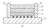
- FIG. 2 is a cross-sectional view illustrating a schematic structure of a light emitting module according to a comparative example.
- the light emitting module 22 is different from the light emitting module 10 according to the first embodiment in the configuration of the first wavelength conversion layer 24 and the second wavelength conversion layer 26.
- the first wavelength conversion layer 24 is obtained by dispersing the same phosphor 1 powder as in Example 1 in a silicone resin.
- the second wavelength conversion layer 26 is obtained by dispersing the same phosphor 2 powder as in Example 1 in a silicone resin.
- Re d phosphors 1,2 so that the light emission color temperature of the white light emitting module is 5500K vicinity, Sr x, the concentration of Eu z are adjusted.
- the first wavelength conversion layer 24 and the second wavelength conversion layer 26 were processed into thicknesses of 100 ⁇ m and 1.2 mm square, respectively. Silicone resin is adhered between the semiconductor light emitting element 14 and the first wavelength conversion layer 24 and between the first wavelength conversion layer 24 and the second wavelength conversion layer 26.
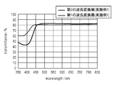
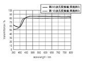
- FIG. 3 is a diagram showing the measurement results of the transmittances of the first wavelength conversion layer 16 and the second wavelength conversion layer 18 according to the first embodiment.
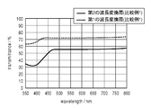
- FIG. 4 is a diagram showing the measurement results of the transmittances of the first wavelength conversion layer 24 and the second wavelength conversion layer 26 according to Comparative Example 1.
- the first wavelength conversion layer 16 and the second wavelength conversion layer 18 according to Example 1 are the first wavelength conversion layer 24 and the second wavelength conversion layer according to Comparative Example 1.
- 26 has a higher transmittance. That is, it can be seen that the layer obtained by converting the phosphor into ceramic has higher transmittance than the layer in which the phosphor is dispersed in the resin.
- FIG. 5 is a diagram showing emission spectra of the light emitting modules according to Example 1 and Comparative Example 1.
- each wavelength conversion layer used in Example 1 has a higher transmittance than each wavelength conversion layer used in Comparative Example 1. For this reason, in the light emitting module 10 according to Example 1, light loss due to scattering is reduced in each wavelength conversion layer. Therefore, the light emitting module 10 according to Example 1 has high emission intensity over almost the entire wavelength range.
- Table 1 shows the luminous flux ratio, luminous efficiency ratio, and color temperature [K] of the light emitting modules according to the examples and comparative examples. Note that the current applied to the light emitting element is 0.7 A.
- the light emitting module 10 according to Example 1 is a highly efficient light emitting module with a luminous flux approximately 1.35 times that of the light emitting module 22 according to Comparative Example 1. Therefore, the light emitting module 10 can save power.
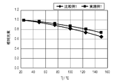
- FIG. 6 is a diagram showing the temperature dependence of the luminous flux in the light emitting modules according to Example 1 and Comparative Example 1.
- the horizontal axis represents the junction temperature (Tj) of the light emitting module
- the vertical axis represents the luminous flux as a relative value.
- the light emitting module 10 according to Example 1 has less decrease in luminous flux as the junction temperature (Tj) increases compared to the light emitting module 22 according to Comparative Example 1.
- the light emitting module 10 using the phosphor layer obtained by converting the phosphor into a ceramic as the wavelength conversion layer has high heat dissipation, it is possible to suppress a decrease in light flux accompanying a temperature rise. In other words, in the light emitting module 10, the temperature dependence of the light flux is reduced.
- Example 2 As shown in FIGS. 3 and 4, when the first wavelength conversion layer 16 according to Example 1 and the first wavelength conversion layer 24 according to Comparative Example 1 using the phosphor 1 are compared, the ceramic layer and the sealing layer are compared. Although there is a difference in the form of a stop resin layer, there is no significant difference in transmittance. In the case of such a phosphor, even if a wavelength conversion layer in which the phosphor powder is sealed with a resin is used, the performance is hardly lowered, and the manufacturing cost can be reduced.
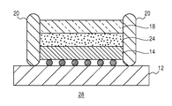
- FIG. 7 is a cross-sectional view illustrating a schematic structure of the light emitting module according to the second embodiment.
- the light emitting module 28 includes the shape, size, and emission color temperature, including the first wavelength conversion layer 24 (see Comparative Example 1) in which a phosphor is dispersed in a resin. 10 is the same configuration.
- the first wavelength conversion layer may be prepared and cut in advance, and then the first wavelength conversion layer and the second wavelength conversion layer made of ceramics may be laminated.
- the wavelength conversion layer is formed by applying the uncured resin of the first wavelength conversion layer onto the semiconductor light emitting element 14 flip-chip bonded to the element mounting substrate 12 by potting or the like, and then forming a second ceramic layer. You may produce by mounting and hardening a wavelength conversion layer. Note that the manufacturing method is not limited to these.
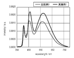
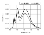
- FIG. 8 is a diagram showing emission spectra of the light emitting modules according to Example 2 and Comparative Example 1.
- the second wavelength conversion layer 18 used in Example 2 has a higher transmittance than the second wavelength conversion layer 26 used in Comparative Example 1. For this reason, in the light emitting module 28 according to Example 2, the light loss due to scattering is reduced particularly in the second wavelength conversion layer 26. Therefore, the light emitting module 28 according to Example 2 has high emission intensity over the entire wavelength range.
- the light emitting module 28 according to Example 2 has a luminous flux approximately 1.28 times that of the light emitting module 22 according to Comparative Example 1, which reduces the manufacturing cost and increases the manufacturing cost. It is a light emitting module that achieves both efficiency and efficiency. Further, the light emitting module 28 having high efficiency can save power.
- Example 3 The light emitting module according to Example 3 is characterized in that the order of stacking the first wavelength conversion layer and the second wavelength conversion layer according to Example 1 is changed.
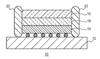
- FIG. 9 is a cross-sectional view illustrating a schematic structure of the light emitting module according to the third embodiment.
- the light emitting module 30 is implemented including the shape, size, and emission color temperature, except that the stacking order of the first wavelength conversion layer 16 and the second wavelength conversion layer 18 is opposite to that of the light emitting module 10 according to the first embodiment.
- the configuration is the same as that of the light emitting module 10 according to Example 1.
- FIG. 10 is a cross-sectional view illustrating a schematic structure of a light emitting module according to Comparative Example 2.
- the light emitting module 32 is a comparison including the shape, size, and emission color temperature, except that the stacking order of the first wavelength conversion layer 24 and the second wavelength conversion layer 26 is opposite to that of the light emitting module 22 according to Comparative Example 1.
- the configuration is the same as that of the light emitting module 22 according to Example 1.
- FIG. 11 is a graph showing the measurement results of the transmittance of the first wavelength conversion layer 16 and the second wavelength conversion layer 18 according to Example 3.
- FIG. 12 is a diagram illustrating the measurement results of the transmittances of the first wavelength conversion layer 24 and the second wavelength conversion layer 26 according to Comparative Example 1.
- the first wavelength conversion layer 16 and the second wavelength conversion layer 18 according to Example 3 are the same as the first wavelength conversion layer 24 and the second wavelength conversion layer according to Comparative Example 2, respectively.
- 26 has a higher transmittance. That is, it can be seen that the first wavelength conversion layer and the second wavelength conversion layer obtained by converting the phosphor into ceramic have higher transmittance than the layer in which the phosphor is dispersed in the resin, regardless of the stacking order.
- FIG. 13 is a diagram showing emission spectra of the light emitting modules according to Example 3 and Comparative Example 2.
- each wavelength conversion layer used in Example 3 has a higher transmittance than each wavelength conversion layer used in Comparative Example 2. For this reason, in the light emitting module 30 according to Example 3, light loss due to scattering is reduced in each wavelength conversion layer. Therefore, the light emitting module 30 according to Example 3 has high emission intensity over almost the entire wavelength range.
- the light emitting module 30 according to Example 3 has a luminous flux approximately 1.37 times that of the light emitting module 32 according to Comparative Example 2, and is a highly efficient light emitting module. is there.
- the light emitting module 32 with high efficiency can save power.
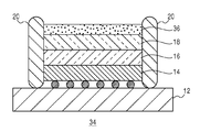
- FIG. 14 is a cross-sectional view illustrating a schematic structure of the light emitting module according to Example 4.
- the light emitting module 34 further includes a third wavelength conversion layer 36 including the phosphor 2 that emits green light on the second wavelength conversion layer 18.
- the configuration is substantially the same as that of the light emitting module 10 according to the first embodiment.
- the third wavelength conversion layer 36 is formed by sealing the phosphor 2 whose general formula is represented by Ba 2-a MgSi 2 O 7 : Eu 2+ a with a resin.
- the light emitting module 34 so that the emission color temperature of the white light emitting module is 5500K vicinity, the concentration of Re d of the phosphor 1 in the first wavelength conversion layer 16 is adjusted, the second wavelength conversion layer 18 The concentrations of Eu z and Sr x of the phosphor 2 in FIG. 3 are adjusted, and the concentration of Eu 2+ a of the phosphor 2 in the third wavelength conversion layer 36 is adjusted.
- the thickness of each of the first wavelength conversion layer 16 and the second wavelength conversion layer 18 is 90 ⁇ m
- the thickness of the third wavelength conversion layer 36 is 50 ⁇ m.
- FIG. 15 is a cross-sectional view illustrating a schematic structure of a light emitting module according to Comparative Example 3.
- the light emitting module 38 further includes a third wavelength conversion layer 36 including the phosphor 2 that emits green light on the second wavelength conversion layer 26.
- the configuration is substantially the same as that of the light emitting module 22 according to Comparative Example 1.
- the third wavelength conversion layer 36 is formed by sealing the phosphor 2 whose general formula is represented by Ba 2-a MgSi 2 O 7 : Eu 2+ a with a resin.
- the light emitting module 38 like the light-emitting module 34 described above, so that the light emission color temperature of the white light emitting module is 5500K vicinity, the concentration of Re d of the phosphor 1 in the first wavelength conversion layer 24 is adjusted Then, the concentrations of Eu z and Sr x of the phosphor 2 in the second wavelength conversion layer 26 are adjusted, and the concentration of Eu 2+ a of the phosphor 2 in the third wavelength conversion layer 36 is adjusted.
- the thickness of each of the first wavelength conversion layer 24 and the second wavelength conversion layer 26 is 90 ⁇ m, and the thickness of the third wavelength conversion layer 36 is 50 ⁇ m.
- FIG. 16 is a diagram showing emission spectra of the light emitting modules according to Example 4 and Comparative Example 3.
- the light emitting module 34 according to Example 4 has small light loss due to scattering in each wavelength conversion layer, and has higher light emission intensity over almost the entire wavelength region than the light emitting module 38 according to Comparative Example 3.
- the light emitting module 34 according to Example 4 has a luminous flux approximately 1.40 times that of the light emitting module 38 according to Comparative Example 1, and is a highly efficient light emitting module. is there. Therefore, the light emitting module 34 can save power.
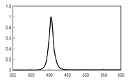
- FIG. 17 is a diagram showing an emission spectrum of the semiconductor light emitting device according to Example 1.
- FIG. 18 is a diagram showing emission spectra of the phosphor 2 according to Example 1 and the conventional YAG phosphor.
- FIG. 19 is a diagram showing excitation spectra of the phosphor 2 according to Example 1 and a conventional YAG phosphor, and emission spectra of the phosphor 1 according to Example 1 and a conventional blue LED.
- the emission spectrum (line L1) of the phosphor 2 according to Example 1 has a blue wavelength (about 450 to 500 nm) compared to the emission spectrum (line L2) of the YAG phosphor. Range).
- a line L1 shown in FIG. 19 represents an excitation spectrum of the phosphor 2 emitting yellow light used in Example 1.
- a line L2 indicates the excitation spectrum of the YAG phosphor.
- the phosphor 2 may satisfy 0.5 ⁇ Imax ⁇ Ia, and may further satisfy 0.8 ⁇ Imax ⁇ Ia as the phosphor 2 illustrated in FIG.
- the phosphor 2 according to the example has high excitation spectrum intensity at the peak wavelength of ultraviolet light or short wavelength visible light emitted from the light emitting element, the light of the light emitting element can be efficiently converted into yellow light.
- the light emitting module which concerns on each Example emits a light emitting element by obtaining white by combining the different color (blue, yellow) each converted by multiple types of fluorescent substance (phosphor 1, phosphor 2). Compared with the case where white is obtained by combining light and light emitted from the phosphor (combination of YAG phosphor and blue LED chip), chromaticity deviation due to the light emission direction of the module is suppressed.
- a line L4 shown in FIG. 19 shows an emission spectrum of the blue-emitting phosphor 1 used in Example 1.
- a light emitting module in which a first wavelength conversion layer 16 including phosphor 1 is stacked on a semiconductor light emitting element 14 and a second wavelength conversion layer 18 including phosphor 2 is stacked thereon.
- the blue light from the phosphor 1 of the first wavelength conversion layer 16 is wavelength-converted by the phosphor 2 of the second wavelength conversion layer 18, heat generation due to so-called Stokes loss occurs, and the light emission efficiency decreases. End up.
- the phosphor 2 according to Example 1 has the maximum excitation spectrum intensity Imax in the wavelength region of 300 nm or more, and the excitation spectrum intensity at the peak wavelength (about 450 nm) of visible light emitted from the phosphor 1 according to Example 1.
- Is Ib, Ib ⁇ 0.8 ⁇ Imax is satisfied.
- the phosphor 2 may satisfy Ib ⁇ 0.5 ⁇ Imax, and may further satisfy Ib ⁇ 0.2 ⁇ Imax as the phosphor 2 illustrated in FIG. Thereby, in the phosphor 2, the absorption of light emitted from the phosphor 1 is reduced, and the Stokes loss is suppressed, so that a highly efficient light emitting module can be realized.
- the phosphor concentration increases compared to a white LED module that combines a blue LED chip and a YAG phosphor. Tend to. This is because the light of the element is not directly used to realize the white color but is realized by the light emitted from the phosphor. For this reason, when the amount of the phosphor is large, the scattering effect by the phosphor is increased as described above, which may be a cause of a decrease in luminous efficiency.
- the second wavelength conversion layer that emits yellow than the first wavelength conversion layer that emits blue emits light flux by arranging it on the emission surface side of the light emitting module.
- the phosphor 2 included in the second wavelength conversion layer includes a relatively large amount of blue wavelength (in the range of about 450 to 500 nm) as described above. Therefore, the amount of blue-emitting phosphor 1 included in the first wavelength conversion layer can be reduced. In this case, it is also possible to select the first wavelength conversion layer in which the phosphor is dispersed in the resin.
- each wavelength conversion layer will be described based on the configuration of the light emitting module 28 shown in Example 2.
- a first wavelength conversion layer 24 in which a blue light emitting phosphor 1 is dispersed in a resin that is a transparent sealing material is laminated on a semiconductor light emitting element 14.
- the second wavelength conversion layer 18 in which the yellow-emitting phosphor 2 is ceramicized is laminated thereon.
- the color temperature of the headlamp is in the range of about 4000 to 6000K. Therefore, if the second wavelength conversion layer is a layer obtained by converting the phosphor 2 into a ceramic, and the first wavelength conversion layer is a layer in which the phosphor 1 is dispersed in a resin, in order to satisfy the light of the color temperature described above,
- the upper limit amount of the concentration of the phosphor 1 contained in the first wavelength conversion layer 16 is 35 vol. %. As shown in Table 2, if the amount of the phosphor necessary for satisfying a desired color temperature is constant, the concentration of the phosphor 1 contained therein decreases as the thickness of the first wavelength conversion layer increases.
- the thickness of the first wavelength conversion layer is preferably in the range of 15 to 1000 ⁇ m. More preferably, the thickness is in the range of 15 to 1000 ⁇ m. If thickness is 15 micrometers or more, the quantity of fluorescent substance 1 which can implement
- the first wavelength conversion layer may contain 0.5 to 35% by volume of the phosphor 1. Thereby, the light of the light emitting element which passes through the first wavelength conversion layer and reaches the second wavelength conversion layer can be increased.
- the light emitted from the phosphor 2 included in the second wavelength conversion layer combined with the first wavelength conversion layer contains a large amount of blue wavelength components as described above, it is included in the first wavelength conversion layer.
- White light can be realized even if the amount of the phosphor 1 emitting blue light is reduced. That is, since the first wavelength conversion layer can be made very thin, the first wavelength conversion layer in which the phosphor 1 is dispersed in an adhesive resin such as a silicone resin is applied on the semiconductor light emitting element, and the second wavelength conversion layer is applied.
- the second wavelength conversion layer can be fixed to the semiconductor light emitting device. That is, the semiconductor light emitting element, the first wavelength conversion layer, and the second wavelength conversion layer 18 can be stacked in one step.
- the thickness of the second wavelength conversion layer may be appropriately selected according to the configuration of the first wavelength conversion layer, and is, for example, in the range of 30 to 1000 ⁇ m, preferably 50 to 300 ⁇ m. If the thickness is 30 ⁇ m or more, it is possible to prevent cracks and the like when it is made into ceramics. On the other hand, if thickness is 1000 micrometers or less, the fall of the brightness
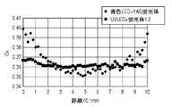
- FIG. 20 is a diagram for explaining a method of measuring the chromaticity of the light emitting module.
- FIG. 21 is a diagram illustrating a change in chromaticity of the light emitting module depending on a measurement position.
- an LED chip 46 that emits blue light or ultraviolet light is mounted on a substrate 42 via a submount 44.
- a fluorescent member 48 is mounted on the light emitting surface of the LED chip 46.
- the change in chromaticity Cx is large depending on the measurement position.
- the UV-LED chip as the LED chip 46, the first wavelength conversion layer 24 having the phosphor 1 as the fluorescent member 48, and the second wavelength conversion layer 18 having the phosphor 2 see Example 2.
- the change in chromaticity Cx depending on the measurement position is very small.
- the configuration of the first and second wavelength conversion layers may be a configuration in which the phosphor is dispersed in an inorganic amorphous material or an inorganic sol-gel material, in addition to being ceramicized or dispersing the phosphor in a resin.
- the inorganic amorphous material include a low melting point glass material.
- the inorganic amorphous material include those having a processing temperature of 900 ° C. or lower, preferably 800 ° C. or lower.
- an inorganic amorphous material having a transmittance of 70% or more, preferably 80% or more is preferable for light having a wavelength of 350 to 900 nm.
- an inorganic amorphous material having a refractive index of 1.4 or more and 2.0 or less, preferably 1.6 or more and 2.0 or less is preferable.
- the light emitting module is described by combining the blue phosphor and the yellow phosphor, but the color combination is not limited to these.
- an aspect of the light emitting module is as follows: A light emitting element emitting ultraviolet light or short wavelength visible light; A first wavelength conversion layer having a first phosphor excited by the ultraviolet light or short wavelength visible light and emitting visible light; A second wavelength having a second phosphor that emits visible light having a peak wavelength longer than a peak wavelength of visible light that is excited by the ultraviolet light or short-wavelength visible light and emitted from the first phosphor.
- a conversion layer, The first wavelength conversion layer and the second wavelength conversion layer are stacked on a light emitting surface of the light emitting element, At least one of the first wavelength conversion layer and the second wavelength conversion layer is a ceramic layer.
- the light emitting module of the present invention can be used for various lamps such as lighting lamps, display backlights, vehicle lamps and the like.
Landscapes
- Led Device Packages (AREA)
Abstract
発光モジュール10は、紫外線又は短波長可視光を発する半導体発光素子14と、紫外線又は短波長可視光により励起され、青色光を発光する第1の蛍光体を有する第1の波長変換層16と、紫外線又は短波長可視光により励起され、黄色光を発光する第2の蛍光体を有する第2の波長変換層18と、を備える。第1の波長変換層16および第2の波長変換層18は、半導体発光素子14の発光面上に積層されており、第1の波長変換層および第2の波長変換層の少なくともいずれか一方は、セラミックス層である。
Description
本発明は、発光モジュールに関する。
従来、照明用の灯具としては蛍光灯や電球が多く用いられてきた。近年、このような灯具の代替として、消費電力や寿命の観点から発光ダイオード(以下、適宜「LED」と称する。)などの半導体発光素子を用いた発光装置が種々開発されている。
このような発光装置では、蛍光体などを用いてLEDなどの発光素子が発する光を波長変換することにより、発光素子が発する光の色とは異なる色の光を出射する発光モジュールを得る技術が知られている。これに対し、光の波長を変換するときの変換効率を増大させるべく、例えば波長変換材料を含むセラミックス層を、発光層によって放出された光の経路内に配置する技術が提案されている(例えば、特許文献1参照)。
ところで、近年、自動車のヘッドランプや照明用の灯具としてLEDを用いた発光モジュールを採用する技術が開発されている。また、これらの灯具では、コストの低減からLEDの数を減らすことが求められており、より高効率な発光モジュールの開発がすすめられている。
本発明はこうした状況に鑑みてなされたものであり、その目的とするところは、高効率な発光モジュールを実現可能な技術を提供することにある。
上記課題を解決するために、本発明のある態様の発光モジュールは、紫外線又は短波長可視光を発する発光素子と、紫外線又は短波長可視光により励起され、青色光を発光する第1の蛍光体を有する第1の波長変換層と、紫外線又は短波長可視光により励起され、黄色光を発光する第2の蛍光体を有する第2の波長変換層と、を備える。第1の波長変換層および第2の波長変換層は、発光素子の発光面上に積層されており、第1の波長変換層および第2の波長変換層の少なくともいずれか一方は、セラミックス層であり、第2の蛍光体は、300nm以上の波長域における励起スペクトルの最大強度をImax、発光素子が発する紫外線又は短波長可視光のピーク波長における励起スペクトルの強度をIaとすると、0.2×Imax<Iaを満たす。
この態様によると、第2の蛍光体は、発光素子が発する紫外線又は短波長可視光のピーク波長における励起スペクトルの強度が高いため、発光素子の光を効率よく黄色光に変換できる。
第1の波長変換層は、発光素子と第2の波長変換層との間に配置されており、第2の波長変換層は、セラミックス層であってもよい。
第2の蛍光体は、300nm以上の波長域における励起スペクトルの最大強度をImax、第1の蛍光体が発する可視光のピーク波長における励起スペクトルの強度をIbとすると、Ib<0.8×Imaxを満たす。これにより、第2の蛍光体において、第1の蛍光体が発する光の吸収を抑えられる。
第1の波長変換層は、第1の蛍光体が透明性の封止材に分散されて構成されており、厚みが15~1000μmであってもよい。
第1の波長変換層は、第1の蛍光体を0.5~35体積%含んでいてもよい。これにより、第1の波長変換層を通過し、第2の波長変換層に到達する発光素子の光を多くできる。
第2の波長変換層は、厚みが30~1000μmであってもよい。
なお、以上の構成要素の任意の組合せ、本発明の表現を方法、装置、システム、などの間で変換したものもまた、本発明の態様として有効である。
本発明によれば、高効率な発光モジュールを実現できる。
はじめに、発明者らが本願発明に想到した背景について説明する。従来、白色LEDモジュールは、近紫外線から青色までの波長の光を発する半導体発光素子に、半導体発光素子が発した光をその光よりも長波長の可視光に変換する蛍光体を組み合わせ、白色光を実現している。
白色LEDモジュールの例としては、青色に発光するLEDチップと黄色に発光するYAG(Yttrium Aluminum Garnet)蛍光体を組み合わせたもの、青色に発光するLEDチップと赤色・緑色にそれぞれ発光する2種類の蛍光体を組み合わせたもの、近紫外線から紫外線に対応する波長の光を発するLEDチップと赤色・緑色・青色にそれぞれ発光する3種類の蛍光体を組み合わせたものなどがある。これらの中で最も一般的なものは、青色LEDチップとYAG蛍光体の組合せである。
LEDモジュールにおける蛍光体層として、粉末状の蛍光体を透明性の封止材(有機樹脂材や無機アモルファス材、無機ゾルゲル材)に分散させた形態とすると、粉末状の蛍光体がフィラーとして作用する。そのため、LEDチップから出射された光を外部に取り出すまでに光損失が発生し、発光モジュールの発光効率を低下させる一因となりうる。これは、蛍光体と封止材の屈折率差が原因であり、この屈折率差により散乱・反射が生じ光損失となる。
そこで、粉末状の蛍光体を焼結させ透光性セラミックス化する手法がある。この手法によれば、蛍光体層は蛍光体単一成分で形成されるため、層内では蛍光体と他の成分との界面は存在せず、屈折率差がなくなり、上述の光損失が大幅に軽減される。その結果、粉末状の蛍光体を透明樹脂に分散させて蛍光体層とした場合と比較して、LEDモジュールの発光効率を高めることができる。現在、高い量子効率を保持したまま透光性セラミックス化に成功している蛍光体はYAGのみである。
しかし、透光性セラミックスYAGと青色LEDとから構成される白色モジュールは、透光性セラミックスYAGより青色LEDの方が発光の指向性が高いので、色が分離する。色分離を抑えるために、透光性セラミックスYAGの中に散乱体成分を添加する手法は有効であるが、一方でセラミックスYAGの透過率が低下し光束が十分得られない。また、このような白色LEDモジュールは、昼白色程度の色温度が高い白色光を実現するのに適している一方、温白色、電球色といった低色温度の光を形成することは困難である。そして、これら低色温度の光を形成するためには、青色光を吸収し赤色に発光する蛍光体を混合するのが一般的であるが、発光面の外周部にレッドリングが形成されやすく、色分離につながる傾向にある。
このような知見に基づいて、本発明者らが鋭意検討した結果、光損失の少ない高効率な発光モジュールを実現すべく以下の構成に着目した。
(1)発光モジュールは、紫外線や短波長可視光(例えば、紫から近紫外の波長の可視光)を発するLEDチップなどの半導体発光素子と、紫外線や短波長可視光を吸収し、可視光で発光する蛍光体を有する蛍光体層と、を備えており、蛍光体層は、蛍光体単一成分で緻密に焼結されたセラミックス層であるとよい。また、セラミックス層は透光性を有することが好ましい。
(2)蛍光体は、発光モジュールとして所望の発光色を得ることができれば、1種類でも複数種類でもよい。
(3)少なくとも1種類以上の蛍光体層がセラミックス層であるとよい。蛍光体の組合せや量によっては、粉末状蛍光体を透明な封止材(有機樹脂材や無機アモルファス材、無機ゾルゲル材)で封止した形状の蛍光体層が含まれていてもよい。この場合、製造コストの低減が図れる。
(4)発光モジュールとしての所望の発光色の違いにより、各色発光の透光性セラミックス蛍光体層同士、透光性セラミックス蛍光体層と粉末状蛍光体を封止した蛍光体層との積層順は限定されず、高効率・色むら抑制などの所望特性により適宜選択することができる。好ましくは、視感度が最も高い色で発光する蛍光体層を最上層(光取り出し面側)に配置するとよい。
(透光性セラミックス蛍光体)
次に、透光性セラミックス蛍光体について説明する。透光性セラミックス蛍光体は、その高い分光透過率を特徴とし、可視光領域を含む波長350~900nmの波長域において透過率(空気中で測定した場合)が70~85%、好ましくは80%以上である。ただし、蛍光体自体の吸収帯(励起帯の波長範囲)ではこの限りではない。また、理論最大透過率(空気中測定)は蛍光体自体の屈折率により一意的に決まる。また、蛍光体媒質内のみの透過率は80~100%、好ましくは90%以上である。ただし、蛍光体自体の吸収帯(励起帯の波長範囲)ではこの限りではない。
次に、透光性セラミックス蛍光体について説明する。透光性セラミックス蛍光体は、その高い分光透過率を特徴とし、可視光領域を含む波長350~900nmの波長域において透過率(空気中で測定した場合)が70~85%、好ましくは80%以上である。ただし、蛍光体自体の吸収帯(励起帯の波長範囲)ではこの限りではない。また、理論最大透過率(空気中測定)は蛍光体自体の屈折率により一意的に決まる。また、蛍光体媒質内のみの透過率は80~100%、好ましくは90%以上である。ただし、蛍光体自体の吸収帯(励起帯の波長範囲)ではこの限りではない。
また、透光性セラミックス蛍光体を発光モジュールに実装する場合、蛍光体層の厚さが40~2000μm、加工性を考慮すれば好ましくは80~2000μmとなるように加工する。また、光の取り出し効率を向上させるため、透光性セラミックス蛍光体表面にフレネルレンズ加工、V字溝加工、レーザ加工、ナノプリンティング加工、イオンミリング、サンドブラスト等の種々の加工による粗面化・パターン化、また任意の屈折率をもつ樹脂やガラス等の白色透明材料を塗布、成膜してもよい。
更に、透光性セラミックス蛍光体は加工性に優れるため、例えばプリズム形状加工、レンズ形状加工、種々のステップ加工、反射材の蒸着などにより、光の取り出し方向や配向制御をすることもできる。また、これらの形状制御は、透光性セラミックス蛍光体の作製過程の成形工程において、あらかじめ所望の形状に成形しておくことで、上記の加工無しで所望形状を付与することもできる。また、鏡面研磨加工とそれに伴い生じる全反射作用を利用し、所定の部位のみの減光、導波、光の取り出し部位の制御等も可能となる。
また、粉末状蛍光体を透明性の封止材(有機樹脂材や無機アモルファス材、無機ゾルゲル材)などで封止した形状の蛍光体層の透過率が、透光性セラミックス蛍光体の透過率と同等である場合は、封止形状の蛍光体層を用いてもよく、製造コストの低減が図れる。この場合、封止形状の蛍光体層の分光透過率は、可視光領域を含む波長350~900nmの波長域において60~85%(空気中で測定)の範囲であり、好ましくは65%以上である。
次に、透光性セラミックス蛍光体の作製方法について概略を説明する。蛍光体の微粒子原料を作製し、必要に応じ適切な焼結助剤を添加する。その後、蛍光体微粒子原料を一軸加圧成形、CIP成形(冷間当方加圧成形)などで成形する。又は、PVA(ポリビニルアルコール)、PVB(ポリビニルブチラール)などの樹脂と混合しスラリー化し、テープ成形、押出成形、鋳込み成形、ゲルキャスティング成形、などで成形する。その後、適切な条件で脱脂、仮焼、必要に応じホットプレス焼成、HIP焼成(熱間当方圧加圧焼成)をして透光性セラミックス蛍光体を得る。その後、所定のサイズに切削・研磨加工し、表面処理加工を施すことで、透光性セラミックス蛍光体が作製される。
上述の知見を考慮した本実施の形態のある態様の発光モジュールは、紫外線又は短波長可視光を発する発光素子と、紫外線又は短波長可視光により励起され、青色光を発光する第1の蛍光体を有する第1の波長変換層と、紫外線又は短波長可視光により励起され、黄色光を発光する第2の蛍光体を有する第2の波長変換層と、を備える。第1の波長変換層および第2の波長変換層は、発光素子の発光面上に積層されており、第1の波長変換層および第2の波長変換層の少なくともいずれか一方は、セラミックス層である。なお、以下の説明では、発光素子としてLEDを例に説明するが、レーザダイオード(LD)素子、エレクトロルミネッセンス(EL)素子等を用いることも可能である。
発光素子は、350~420nmの波長域にピーク波長を有する紫外線又は短波長可視光を発しているものが好ましい。これにより、発光スペクトルの異なる複数種の蛍光体、例えば、各実施例に係る青色蛍光体と黄色蛍光体を用いて白色光を実現できる。また、発光素子の光を直接用いずに青色光と黄色光との混色で白色光を実現できる。
このように、少なくとも1種類の蛍光体を含む層をセラミックス層とすることで、蛍光体層の透過率が向上し、散乱ロスが大幅に軽減されるため、発光モジュールとして高効率化が図れる。
具体的には、発光モジュールとしての白色LEDモジュールは、近紫外光を発するLEDチップと、近紫外光を吸収し青色光を発する第1の蛍光体(蛍光体1)と、近紫外光を吸収し黄色光を発する第2の蛍光体(蛍光体2)とを有する。そして、第1の蛍光体と第2の蛍光体の少なくともいずれかをセラミックス板化することで、新規な白色LEDモジュールが得られる。第1の蛍光体が発する青色光は、例えば、ピーク波長λpが400~500nm程度の光である。また、第2の蛍光体が発する黄色光は、例えば、ピーク波長λpが500~620nm程度の光であり、より好ましくは、視感度がピークとなる555nm近傍にピーク波長λを有する光がよい。
このように、近紫外光を発するLEDチップと複数種の蛍光体を組み合わせた白色LEDモジュールは、実質的に、全方向に発光する蛍光体の蛍光のみで白色を形成するため、色分離が生じづらい。この際、複数種の蛍光体の中で、相対的に長波長で発光する蛍光体は、相対的に短波長で発光する蛍光体の蛍光を吸収し発光しないことが重要である。そこで、本実施の形態の好適な例としては、以下に示す、相対的に短波長で発光する蛍光体1と、相対的に長波長で発光する蛍光体2と、を挙げて説明する。
(蛍光体1)
本実施の形態に係る蛍光体1は、紫外光又は短波長可視光により励起され、青色で発光する青色蛍光体である。例えば、
(i)一般式がM1 a(M2O4)bXc:Redで表されている蛍光体
(M1は、Ca、Sr、Baのうち一種以上を必須とし、一部をMg、Zn、Cd、K、Ag、Tlからなる群の元素に置き換えることができる。M2は、Pを必須とし、一部をV,Si,As,Mn,Co,Cr,Mo,W,Bからなる群の元素に置き換えることができる。Xは少なくとも1種のハロゲン元素、Reは、Eu2+必須とする少なくとも1種の希土類元素又はMnを示す。aは4.2≦a≦5.8、bは2.5≦b≦3.5、cは0.8<c<1.4、dは0.01<d<0.1の範囲である。)
本実施の形態に係る蛍光体1は、紫外光又は短波長可視光により励起され、青色で発光する青色蛍光体である。例えば、
(i)一般式がM1 a(M2O4)bXc:Redで表されている蛍光体
(M1は、Ca、Sr、Baのうち一種以上を必須とし、一部をMg、Zn、Cd、K、Ag、Tlからなる群の元素に置き換えることができる。M2は、Pを必須とし、一部をV,Si,As,Mn,Co,Cr,Mo,W,Bからなる群の元素に置き換えることができる。Xは少なくとも1種のハロゲン元素、Reは、Eu2+必須とする少なくとも1種の希土類元素又はMnを示す。aは4.2≦a≦5.8、bは2.5≦b≦3.5、cは0.8<c<1.4、dは0.01<d<0.1の範囲である。)
(ii)一般式がM1
1-aMgAl10O17:Eu2+
aで表されている蛍光体
(M1は、Ca、Sr、Ba、Znからなる群より選ばれる少なくとも1種の元素、aは0.001≦a≦0.5の範囲である。)
(M1は、Ca、Sr、Ba、Znからなる群より選ばれる少なくとも1種の元素、aは0.001≦a≦0.5の範囲である。)
(iii)一般式がM1
1-aMgSi2O8:Eu2+
aで表されている蛍光体
(M1は、Ca、Sr、Ba、Znからなる群より選ばれる少なくとも1種の元素、aは0.001≦a≦0.8の範囲である。)
(M1は、Ca、Sr、Ba、Znからなる群より選ばれる少なくとも1種の元素、aは0.001≦a≦0.8の範囲である。)
(iv)一般式がM1
2-a(B5O9)X:Reaで表されている蛍光体
(M1は、Ca、Sr、Ba、Znからなる群より選ばれる少なくとも1種の元素、Xは少なくとも1種のハロゲン元素、aは0.001≦a≦0.5の範囲である。)
(M1は、Ca、Sr、Ba、Znからなる群より選ばれる少なくとも1種の元素、Xは少なくとも1種のハロゲン元素、aは0.001≦a≦0.5の範囲である。)
(蛍光体2)
本実施の形態に係る蛍光体2は、紫外光又は短波長可視光により励起され、緑~黄色で発光する蛍光体である。例えば、
(i)一般式が(Ca1-x-y-z-w、Srx、MII y、Euz、MR w)7(SiO3)6X2で表されている蛍光体
(MIIは、Mg、Ba又はZn、MRは希土類元素又はMn、Xは、Cl又はClを必須とする複数のハロゲン元素、xは0.1<x<0.7、yは0≦y<0.3、zは0<z<0.4、wは0≦w<0.1の範囲である。)
本実施の形態に係る蛍光体2は、紫外光又は短波長可視光により励起され、緑~黄色で発光する蛍光体である。例えば、
(i)一般式が(Ca1-x-y-z-w、Srx、MII y、Euz、MR w)7(SiO3)6X2で表されている蛍光体
(MIIは、Mg、Ba又はZn、MRは希土類元素又はMn、Xは、Cl又はClを必須とする複数のハロゲン元素、xは0.1<x<0.7、yは0≦y<0.3、zは0<z<0.4、wは0≦w<0.1の範囲である。)
(ii)一般式がCsM1
1-a P2O7:Eu2+
aで表されている蛍光体
(M1はCa、Sr、aは0.001≦a≦0.5の範囲である。)
(iii)一般式がBa2-aMgSi2O7:Eu2+ aで表されている蛍光体
(aは0.001≦a≦0.5の範囲である。)
(M1はCa、Sr、aは0.001≦a≦0.5の範囲である。)
(iii)一般式がBa2-aMgSi2O7:Eu2+ aで表されている蛍光体
(aは0.001≦a≦0.5の範囲である。)
このような蛍光体2は、前述の蛍光体1と混合されても、蛍光体1が発する青色光をほとんど吸収しないため、色分離抑制に有効であり、色度もずれにくい。また、青色に発光する蛍光体と組み合わせることで電球色から昼光色までの幅広い白色を形成可能である。
以下に、本実施の形態に係る透光性セラミックス蛍光体層を有する発光モジュールの幾つかの効果を挙げる。
(1)発光モジュール内の色安定性
近紫外光を発するLEDチップと、上述の蛍光体1、蛍光体2を組み合わせた白色LEDモジュールは、製造工法に由来する近紫外発光LEDチップの強度差、波長ずれに対し白色の色度がずれにくい。
(1)発光モジュール内の色安定性
近紫外光を発するLEDチップと、上述の蛍光体1、蛍光体2を組み合わせた白色LEDモジュールは、製造工法に由来する近紫外発光LEDチップの強度差、波長ずれに対し白色の色度がずれにくい。
(2)高効率(省電力)
InGaN系LEDに代表される近紫外発光LEDチップは、同系の青色発光LEDチップに対し、原理的には1.2倍高効率であり、特にパワー系発光モジュールにおいては有効なLEDチップである。そして、少なくとも1種類の蛍光体を透光性セラミックス化することで蛍光体層における散乱を軽減し、高効率化(省電力化)が可能となる。
InGaN系LEDに代表される近紫外発光LEDチップは、同系の青色発光LEDチップに対し、原理的には1.2倍高効率であり、特にパワー系発光モジュールにおいては有効なLEDチップである。そして、少なくとも1種類の蛍光体を透光性セラミックス化することで蛍光体層における散乱を軽減し、高効率化(省電力化)が可能となる。
(3)温度特性の向上
パワー系発光モジュールとしての使用を想定した場合、蛍光体のストークスロスによる発熱量が大きくなり、この放熱が重要となる。蛍光体自体の熱伝導率は、一般的な封止材(例えば、シリコーン系樹脂、エポキシ系樹脂などが挙げられる。)に対し2倍以上であるため、蛍光体の透光性セラミックス化により放熱性が大きく改善され、発光モジュールとしての温度特性が向上する。
パワー系発光モジュールとしての使用を想定した場合、蛍光体のストークスロスによる発熱量が大きくなり、この放熱が重要となる。蛍光体自体の熱伝導率は、一般的な封止材(例えば、シリコーン系樹脂、エポキシ系樹脂などが挙げられる。)に対し2倍以上であるため、蛍光体の透光性セラミックス化により放熱性が大きく改善され、発光モジュールとしての温度特性が向上する。
(4)信頼性の向上
一般的に有機物は紫外線に弱い。そこで、複数の蛍光体層を全て透光性セラミックス板化し、更に蛍光体層間、蛍光体層-LEDチップ間の接着をゾルゲル接着剤等を用いた場合は、有機物レスの発光モジュールを実現でき、パワー系発光モジュールとしての信頼性が大幅に向上する。
一般的に有機物は紫外線に弱い。そこで、複数の蛍光体層を全て透光性セラミックス板化し、更に蛍光体層間、蛍光体層-LEDチップ間の接着をゾルゲル接着剤等を用いた場合は、有機物レスの発光モジュールを実現でき、パワー系発光モジュールとしての信頼性が大幅に向上する。
以下、図面を参照しながら、本発明を実施するための形態の実施例について詳細に説明する。なお、図面の説明において同一の要素には同一の符号を付し、重複する説明を適宜省略する。
(実施例1)
図1は、実施例1に係る発光モジュールの概略構造を示す断面図である。発光モジュール10は、素子搭載用基板12と、素子搭載用基板12の上にフリップチップ実装されている半導体発光素子14と、半導体発光素子14の発光面上に設けられている第1の波長変換層16と、第1の波長変換層16の上に設けられている第2の波長変換層18と、を備えている。ここで、「層の上に設けられ」とは、層の上に直接設けられている場合だけでなく、層の上に他の部材(接着剤やフィルタ等)を介して間接的に設けられている場合も含まれる。
(実施例1)
図1は、実施例1に係る発光モジュールの概略構造を示す断面図である。発光モジュール10は、素子搭載用基板12と、素子搭載用基板12の上にフリップチップ実装されている半導体発光素子14と、半導体発光素子14の発光面上に設けられている第1の波長変換層16と、第1の波長変換層16の上に設けられている第2の波長変換層18と、を備えている。ここで、「層の上に設けられ」とは、層の上に直接設けられている場合だけでなく、層の上に他の部材(接着剤やフィルタ等)を介して間接的に設けられている場合も含まれる。
半導体発光素子14は、ピーク波長λp=405nmのLEDチップである。第1の波長変換層16は、一般式がM1
a(M2O4)bXc:Redで表されている蛍光体1を有している。また、第2の波長変換層18は、一般式が(Ca1-x-y-z-w、Srx、MII
y、Euz、MR
w)7(SiO3)6X2で表されている蛍光体2を有している。積層された半導体発光素子14、第1の波長変換層16および第2の波長変換層18の側面は、光反射材20で覆われている。
第1の波長変換層16および第2の波長変換層18のそれぞれは、あらかじめ作製されているサブミクロン以下の各蛍光体の粒子を、適切な焼結助剤と混合し成形した後、一軸加圧成形、CIP成形、常圧焼成、HIP焼成等の処理が行われ、その後、厚さ100μmとなるように薄肉化・研磨され、透光性セラミックス化される。この際、白色発光モジュールとしての発光色温度が5500K近傍となるように蛍光体1、2のRed、Srx、Euzの濃度が調整されている。その後、透光性セラミックス蛍光体である、第1の波長変換層16および第2の波長変換層18を、それぞれ厚さ100μm、1.2mm角に加工した。半導体発光素子14と第1の波長変換層16との間、第1の波長変換層16と第2の波長変換層18との間は、ゾルゲル系接着剤により接着されている。
(比較例1)
図2は、比較例に係る発光モジュールの概略構造を示す断面図である。発光モジュール22は、第1の波長変換層24および第2の波長変換層26の構成が実施例1に係る発光モジュール10と異なる。第1の波長変換層24は、実施例1と同様の蛍光体1の粉末をシリコーン樹脂に分散させたものである。また、第2の波長変換層26は、実施例1と同様の蛍光体2の粉末をシリコーン樹脂に分散させたものである。この際、白色発光モジュールとしての発光色温度が5500K近傍となるように蛍光体1、2のRed、Srx、Euzの濃度が調整されている。その後、第1の波長変換層24および第2の波長変換層26を、それぞれ厚さ100μm、1.2mm角に加工した。半導体発光素子14と第1の波長変換層24との間、第1の波長変換層24と第2の波長変換層26との間は、シリコーン樹脂により接着されている。
図2は、比較例に係る発光モジュールの概略構造を示す断面図である。発光モジュール22は、第1の波長変換層24および第2の波長変換層26の構成が実施例1に係る発光モジュール10と異なる。第1の波長変換層24は、実施例1と同様の蛍光体1の粉末をシリコーン樹脂に分散させたものである。また、第2の波長変換層26は、実施例1と同様の蛍光体2の粉末をシリコーン樹脂に分散させたものである。この際、白色発光モジュールとしての発光色温度が5500K近傍となるように蛍光体1、2のRed、Srx、Euzの濃度が調整されている。その後、第1の波長変換層24および第2の波長変換層26を、それぞれ厚さ100μm、1.2mm角に加工した。半導体発光素子14と第1の波長変換層24との間、第1の波長変換層24と第2の波長変換層26との間は、シリコーン樹脂により接着されている。
図3は、実施例1に係る第1の波長変換層16および第2の波長変換層18の透過率の測定結果を示す図である。図4は、比較例1に係る第1の波長変換層24および第2の波長変換層26の透過率の測定結果を示す図である。図3、図4に示す通り、実施例1に係る第1の波長変換層16および第2の波長変換層18は、比較例1に係る第1の波長変換層24および第2の波長変換層26に対して透過率が高い。つまり、蛍光体をセラミックス化した層の方が、蛍光体を樹脂に分散させた層よりも透過率が高いことがわかる。
図5は、実施例1および比較例1に係る発光モジュールの発光スペクトルを示す図である。前述のように、実施例1で用いられている各波長変換層は、比較例1で用いられている各波長変換層と比較して、透過率が高い。このため、実施例1に係る発光モジュール10は、各波長変換層において散乱による光損失が小さくなる。そのため、実施例1に係る発光モジュール10は、波長域のほぼ全体にわたって発光強度が高い。
表1は、各実施例および各比較例に係る発光モジュールの光束比、発光効率比、色温度[K]を示したものである。なお、発光素子への印加電流は0.7Aである。

表1に示すように、実施例1に係る発光モジュール10は、比較例1に係る発光モジュール22と比較して、光束が約1.35倍となっており、高効率な発光モジュールである。そのため、発光モジュール10は、省電力化が可能である。
図6は、実施例1および比較例1に係る発光モジュールにおける光束の温度依存性を示す図である。図6において、横軸は発光モジュールのジャンクション温度(Tj)を表し、縦軸は光束を相対値で表している。
図6に示すように、実施例1に係る発光モジュール10は、比較例1に係る発光モジュール22と比較して、ジャンクション温度(Tj)の上昇に伴う光束の低下が少ない。具体的には、実施例1に係る発光モジュール10は、比較例1に係る発光モジュール22と比較して、光束がTj=50℃において2.3%、Tj=100℃において6.8%、Tj=150℃において11.3%向上している。このように、蛍光体をセラミックス化した蛍光体層を波長変換層として用いた発光モジュール10は、放熱性が高いため、温度上昇に伴う光束の低下を抑制できる。換言すると、発光モジュール10は、光束の温度依存性が低減されている。
(実施例2)
図3、図4に示すように、蛍光体1を用いた、実施例1に係る第1の波長変換層16と比較例1に係る第1の波長変換層24を比較すると、セラミックス層と封止樹脂層という形態の違いがあるものの、透過率に大きな差はない。このような蛍光体の場合には、蛍光体の粉末を樹脂で封止した波長変換層を用いても性能の低下はほとんどなく、製造コストを低減できる。
図3、図4に示すように、蛍光体1を用いた、実施例1に係る第1の波長変換層16と比較例1に係る第1の波長変換層24を比較すると、セラミックス層と封止樹脂層という形態の違いがあるものの、透過率に大きな差はない。このような蛍光体の場合には、蛍光体の粉末を樹脂で封止した波長変換層を用いても性能の低下はほとんどなく、製造コストを低減できる。
図7は、実施例2に係る発光モジュールの概略構造を示す断面図である。発光モジュール28は、蛍光体が樹脂に分散された第1の波長変換層24(比較例1参照)を用いている点以外は、形状、大きさや発光色温度を含め実施例1に係る発光モジュール10と同じ構成である。波長変換層は、予め第1の波長変換層を作製しカッティングした後、この第1の波長変換層およびセラミックスからなる第2の波長変換層を積層してもよい。また、波長変換層は、第1の波長変換層の未硬化樹脂を、素子搭載用基板12にフリップチップボンディングされている半導体発光素子14上にポッティング等で塗布した後、セラミックスからなる第2の波長変換層を実装して硬化することで作製してもよい。なお、作製方法はこれらに限られない。
図8は、実施例2および比較例1に係る発光モジュールの発光スペクトルを示す図である。前述のように、実施例2で用いられている第2の波長変換層18は、比較例1で用いられている第2の波長変換層26と比較して、透過率が高い。このため、実施例2に係る発光モジュール28は、特に第2の波長変換層26において散乱による光損失が小さくなる。そのため、実施例2に係る発光モジュール28は、波長域全体にわたって発光強度が高い。
また、表1に示すように、実施例2に係る発光モジュール28は、比較例1に係る発光モジュール22と比較して、光束が約1.28倍となっており、製造コストの低減と高効率とが両立された発光モジュールである。また、効率が高い発光モジュール28は、省電力化が可能である。
(実施例3)
実施例3に係る発光モジュールは、実施例1に係る第1の波長変換層および第2の波長変換層の積層順を変更した点が特徴の一つである。図9は、実施例3に係る発光モジュールの概略構造を示す断面図である。発光モジュール30は、第1の波長変換層16と第2の波長変換層18の積層順を、実施例1に係る発光モジュール10と反対にした以外は、形状、大きさや発光色温度を含め実施例1に係る発光モジュール10と同じ構成である。
実施例3に係る発光モジュールは、実施例1に係る第1の波長変換層および第2の波長変換層の積層順を変更した点が特徴の一つである。図9は、実施例3に係る発光モジュールの概略構造を示す断面図である。発光モジュール30は、第1の波長変換層16と第2の波長変換層18の積層順を、実施例1に係る発光モジュール10と反対にした以外は、形状、大きさや発光色温度を含め実施例1に係る発光モジュール10と同じ構成である。
(比較例2)
比較例2に係る発光モジュールは、比較例1に係る第1の波長変換層および第2の波長変換層の積層順を変更した点が特徴の一つである。図10は、比較例2に係る発光モジュールの概略構造を示す断面図である。発光モジュール32は、第1の波長変換層24と第2の波長変換層26の積層順を、比較例1に係る発光モジュール22と反対にした以外は、形状、大きさや発光色温度を含め比較例1に係る発光モジュール22と同じ構成である。
比較例2に係る発光モジュールは、比較例1に係る第1の波長変換層および第2の波長変換層の積層順を変更した点が特徴の一つである。図10は、比較例2に係る発光モジュールの概略構造を示す断面図である。発光モジュール32は、第1の波長変換層24と第2の波長変換層26の積層順を、比較例1に係る発光モジュール22と反対にした以外は、形状、大きさや発光色温度を含め比較例1に係る発光モジュール22と同じ構成である。
図11は、実施例3に係る第1の波長変換層16および第2の波長変換層18の透過率の測定結果を示す図である。図12は、比較例1に係る第1の波長変換層24および第2の波長変換層26の透過率の測定結果を示す図である。図11、図12に示す通り、実施例3に係る第1の波長変換層16および第2の波長変換層18は、比較例2に係る第1の波長変換層24および第2の波長変換層26に対して透過率が高い。つまり、蛍光体をセラミックス化した第1の波長変換層および第2の波長変換層は、積層順にかかわらず、蛍光体を樹脂に分散させた層よりも透過率が高いことがわかる。
図13は、実施例3および比較例2に係る発光モジュールの発光スペクトルを示す図である。前述のように、実施例3で用いられている各波長変換層は、比較例2で用いられている各波長変換層と比較して、透過率が高い。このため、実施例3に係る発光モジュール30は、各波長変換層において散乱による光損失が小さくなる。そのため、実施例3に係る発光モジュール30は、波長域のほぼ全体にわたって発光強度が高い。
また、表1に示すように、実施例3に係る発光モジュール30は、比較例2に係る発光モジュール32と比較して、光束が約1.37倍となっており、高効率な発光モジュールである。また、効率が高い発光モジュール32は、省電力化が可能である。
(実施例4)
図14は、実施例4に係る発光モジュールの概略構造を示す断面図である。発光モジュール34は、第2の波長変換層18の上に、緑色で発光する蛍光体2を含む第3の波長変換層36を更に備えている点が特徴の一つであり、それ以外は、概ね実施例1に係る発光モジュール10と同様の構成である。第3の波長変換層36は、一般式がBa2-aMgSi2O7:Eu2+ aで表されている蛍光体2が樹脂で封止されたものである。
図14は、実施例4に係る発光モジュールの概略構造を示す断面図である。発光モジュール34は、第2の波長変換層18の上に、緑色で発光する蛍光体2を含む第3の波長変換層36を更に備えている点が特徴の一つであり、それ以外は、概ね実施例1に係る発光モジュール10と同様の構成である。第3の波長変換層36は、一般式がBa2-aMgSi2O7:Eu2+ aで表されている蛍光体2が樹脂で封止されたものである。
なお、発光モジュール34は、白色発光モジュールとしての発光色温度が5500K近傍となるように、第1の波長変換層16における蛍光体1のRedの濃度が調整され、第2の波長変換層18における蛍光体2のEuz、Srxの濃度が調整され、第3の波長変換層36における蛍光体2のEu2+
aの濃度が調整されている。また、実施例4においては、第1の波長変換層16および第2の波長変換層18のそれぞれの厚みを90μm、第3の波長変換層36の厚みを50μmとしている。
(比較例3)
図15は、比較例3に係る発光モジュールの概略構造を示す断面図である。発光モジュール38は、第2の波長変換層26の上に、緑色で発光する蛍光体2を含む第3の波長変換層36を更に備えている点が特徴の一つであり、それ以外は、概ね比較例1に係る発光モジュール22と同様の構成である。第3の波長変換層36は、一般式がBa2-aMgSi2O7:Eu2+ aで表されている蛍光体2が樹脂で封止されたものである。
図15は、比較例3に係る発光モジュールの概略構造を示す断面図である。発光モジュール38は、第2の波長変換層26の上に、緑色で発光する蛍光体2を含む第3の波長変換層36を更に備えている点が特徴の一つであり、それ以外は、概ね比較例1に係る発光モジュール22と同様の構成である。第3の波長変換層36は、一般式がBa2-aMgSi2O7:Eu2+ aで表されている蛍光体2が樹脂で封止されたものである。
なお、発光モジュール38は、前述の発光モジュール34と同様に、白色発光モジュールとしての発光色温度が5500K近傍となるように、第1の波長変換層24における蛍光体1のRedの濃度が調整され、第2の波長変換層26における蛍光体2のEuz、Srxの濃度が調整され、第3の波長変換層36における蛍光体2のEu2+
aの濃度が調整されている。また、比較例3においては、第1の波長変換層24および第2の波長変換層26のそれぞれの厚みを90μm、第3の波長変換層36の厚みを50μmとしている。
図16は、実施例4および比較例3に係る発光モジュールの発光スペクトルを示す図である。実施例4に係る発光モジュール34は、各波長変換層において散乱による光損失が小さく、比較例3に係る発光モジュール38と比較して、波長域のほぼ全体にわたって発光強度が高い。
また、表1に示すように、実施例4に係る発光モジュール34は、比較例1に係る発光モジュール38と比較して、光束が約1.40倍となっており、高効率な発光モジュールである。そのため、発光モジュール34は、省電力化が可能である。
次に、発光モジュールの更に好適な構成について説明する。はじめに、半導体発光素子の発光スペクトル、各蛍光体の発光スペクトルおよび励起スペクトルについて説明する。図17は、実施例1に係る半導体発光素子の発光スペクトルを示す図である。図18は、実施例1に係る蛍光体2および従来のYAG蛍光体の発光スペクトルを示す図である。図19は、実施例1に係る蛍光体2および従来のYAG蛍光体の励起スペクトル、並びに、実施例1に係る蛍光体1および従来の青色LEDの発光スペクトルを示す図である。
図17に示すように、実施例に係る半導体発光素子は、ピーク波長λp=405nmの近紫外光を発するLEDである。また、図18に示すように、実施例1に係る蛍光体2の発光スペクトル(ラインL1)は、YAG蛍光体の発光スペクトル(ラインL2)と比較して、青色の波長(約450~500nmの範囲)を多く含む。
図19に示すラインL1は、実施例1で使用した黄色発光の蛍光体2の励起スペクトルを示している。また、ラインL2は、YAG蛍光体の励起スペクトルを示している。両者を比較すると、励起光の波長域が大きく異なっていることがわかる。YAG蛍光体は、発光素子が発する紫外線又は短波長可視光のピーク波長(λp=405nm)における励起スペクトルの強度Iyは小さく、近紫外光では発光しないことがわかる。そのため、YAG蛍光体と組み合わせて白色を実現するためには、図19に示すような発光スペクトル(ラインL3)特性を有する青色発光LEDチップが必要である。
一方、蛍光体2は、300nm以上の波長域における励起スペクトル(L1)の最大強度をImax、発光素子が発する紫外線又は短波長可視光のピーク波長(λp=405nm)における励起スペクトルの強度をIaとすると、0.2×Imax<Iaを満たしている。好ましくは、蛍光体2は、0.5×Imax<Iaを満たしているとよく、図19に示す蛍光体2のように、0.8×Imax<Iaを満たしていると更によい。
これにより、実施例に係る蛍光体2は、発光素子が発する紫外線又は短波長可視光のピーク波長における励起スペクトルの強度が高いため、発光素子の光を効率よく黄色光に変換できる。
また、各実施例に係る発光モジュールは、複数種の蛍光体(蛍光体1、蛍光体2)でそれぞれ変換された異なる色(青色、黄色)を組み合わせて白色を得ることで、発光素子が発する光と蛍光体が発する光とを組み合わせて白色を得る場合(YAG蛍光体と青色LEDチップとの組合せ)と比較して、モジュールの発光方向による色度ずれが抑えられる。
図19に示すラインL4は、実施例1で使用した青色発光の蛍光体1の発光スペクトルを示している。実施例1に示すように半導体発光素子14の上に蛍光体1を含む第1の波長変換層16を積層し、その上に蛍光体2を含む第2の波長変換層18を積層した発光モジュールの場合、第1の波長変換層16の蛍光体1による青色光が、第2の波長変換層18の蛍光体2で波長変換されると、いわゆるストークスロスによる発熱が生じ、発光効率が低下してしまう。
しかしながら、実施例1に係る蛍光体2は、300nm以上の波長域における励起スペクトルの最大強度をImax、実施例1に係る蛍光体1が発する可視光のピーク波長(約450nm)における励起スペクトルの強度をIbとすると、Ib<0.8×Imaxを満たす。好ましくは、蛍光体2は、Ib<0.5×Imaxを満たしているとよく、図19に示す蛍光体2のように、Ib<0.2×Imaxを満たしていると更によい。これにより、蛍光体2において、蛍光体1が発する光の吸収が少なくなり、ストークスロスが抑えられため、高効率な発光モジュールが実現できる。
ここで、近紫外光を発する半導体発光素子と複数種の蛍光体とを組み合わせた白色発光モジュールでは、青色LEDチップとYAG蛍光体とを組み合わせた白色LEDモジュールと比較して、蛍光体濃度が増加する傾向にある。これは、白色を実現するために素子の光を直接利用せず、ほとんど蛍光体から発する光で実現しているためである。そのため、蛍光体の量が多いと、前述の通り蛍光体による散乱効果が大きくなり発光効率が低下する一因ともなりうる。
そこで、以下では、上述の実施の形態や実施例で得られた知見に基づいて、蛍光体濃度を抑えつつ高い発光効率を実現する発光モジュールの構成について更に詳述する。
青色と黄色を比較すると、黄色の方が視感度が高いため、青色を発する第1の波長変換層よりも黄色を発する第2の波長変換層を発光モジュールの出射面側に配置することで光束を高められる(表1の実施例1と実施例3を参照。)。また、第2の波長変換層に含まれる蛍光体2は、前述のように青色の波長(約450~500nmの範囲)を比較的多く含む。そのため、第1の波長変換層に含ませる青色発光の蛍光体1の量を低減できる。この場合、蛍光体が樹脂に分散された第1の波長変換層を選択することも可能である。
そこで、以下では、実施例2に示す発光モジュール28の構成を基準に各波長変換層の厚みの好適な例について説明する。図7に示すように、発光モジュール28は、半導体発光素子14の上に、青色発光の蛍光体1が透明性の封止材である樹脂に分散された第1の波長変換層24が積層され、その上に黄色発光の蛍光体2がセラミックス化された第2の波長変換層18が積層された構造である。
発光モジュールを自動車用ヘッドランプの光源として使用する場合、ヘッドランプの色温度は4000~6000K程度の範囲である。そこで、第2の波長変換層は蛍光体2をセラミックス化した層とし、第1の波長変換層は樹脂に蛍光体1を分散させた層とすると、前述の色温度の光を満たすためには、第1の波長変換層16に含ませられる蛍光体1の濃度の上限量は、製法上の観点から35vol.%程度である。表2に示すように、所望の色温度を満たすために必要な蛍光体の量が一定だとすると、第1の波長変換層の厚みが厚くなると、そこに含まれる蛍光体1の濃度は低下する。

第1の波長変換層は、厚みが15~1000μmの範囲が好ましい。より好ましくは、厚みが15~1000μmの範囲である。厚みが15μm以上であれば、所望の色温度を実現できる量の蛍光体1を含ませることができる。一方、厚みが1000μm以下、好ましくは300μm以下であれば、第1の波長変換層の内部での光の吸収や散乱が抑えられる。また、第1の波長変換層は、蛍光体1を0.5~35体積%含んでいてもよい。これにより、第1の波長変換層を通過し、第2の波長変換層に到達する発光素子の光を多くできる。
また、第1の波長変換層と組み合わせる第2の波長変換層に含まれる蛍光体2が発する光は、前述のように青色の波長成分を多く含んでいるため、第1の波長変換層に含ませる青色発光の蛍光体1の量を少なくしても白色光を実現できる。つまり、第1の波長変換層を非常に薄くできるため、第1の波長変換層としてシリコーン樹脂などの接着性の樹脂に蛍光体1を分散させたものを半導体発光素子上に塗布し、第2の波長変換層を積層することで第2の波長変換層を半導体発光素子に固定できる。つまり、半導体発光素子と第1の波長変換層と第2の波長変換層18とを一つの工程で積層できる。
第2の波長変換層の厚みは、第1の波長変換層の構成に応じて適宜選択すればよいが、例えば、30~1000μm、好ましくは、50~300μmの範囲である。厚みが30μm以上であれば、セラミックス化した際の割れなどを防止できる。一方、厚みが1000μm以下であれば、発光モジュールの輝度の低下を抑制できる。
図20は、発光モジュールの色度を測定する方法を説明するための図である。図21は、測定位置による発光モジュールの色度の変化を示す図である。
図20に示す発光モジュール40は、基板42の上にサブマウント44を介して青色光又は紫外光を発するLEDチップ46が搭載されている。LEDチップ46の発光面上には、蛍光部材48が搭載されている。
図21に示すように、LEDチップ46として青色LEDチップを、蛍光部材48としてYAG蛍光体を採用した発光モジュールでは、測定位置によって色度Cxの変化が大きい。これに対して、LEDチップ46としてUV-LEDチップを、蛍光部材48として蛍光体1を有する第1の波長変換層24および蛍光体2を有する第2の波長変換層18(実施例2参照)を採用した発光モジュールでは、測定位置による色度Cxの変化が非常に少ない。
以上、本発明を実施の形態や実施例をもとに説明した。この実施の形態や実施例は例示であり、それらの各構成要素や各処理プロセスの組合せにいろいろな変形例が可能なこと、またそうした変形例も本発明の範囲にあることは当業者に理解されるところである。
例えば、第1や第2の波長変換層の構成として、セラミックス化したり樹脂に蛍光体を分散させたりする以外に、無機アモルファス材や無機ゾルゲル材に蛍光体を分散させた構成であってもよい。無機アモルファス材としては、例えば、低融点ガラス材が挙げられる。無機アモルファス材は、処理温度が900℃以下、好ましくは800℃以下のものが挙げられる。また、波長350~900nmの光において、透過率が70%以上、好ましくは80%以上の無機アモルファス材が好ましい。また、屈折率が1.4以上、2.0以下、好ましくは、1.6以上、2.0以下の無機アモルファス材が好ましい。
上述の各実施例では、青色蛍光体と黄色蛍光体とを組み合わせ発光モジュールについて説明したが、色の組合せはこれらに限られない。
例えば、ある態様の発光モジュールは、
紫外線又は短波長可視光を発する発光素子と、
前記紫外線又は短波長可視光により励起され、可視光を発光する第1の蛍光体を有する第1の波長変換層と、
前記紫外線又は短波長可視光により励起され、第1の蛍光体が発光する可視光のピーク波長よりも長波長側のピーク波長を有する可視光を発光する第2の蛍光体を有する第2の波長変換層と、を備え、
前記第1の波長変換層および前記第2の波長変換層は、前記発光素子の発光面上に積層されており、
前記第1の波長変換層および前記第2の波長変換層の少なくともいずれか一方は、セラミックス層である。
紫外線又は短波長可視光を発する発光素子と、
前記紫外線又は短波長可視光により励起され、可視光を発光する第1の蛍光体を有する第1の波長変換層と、
前記紫外線又は短波長可視光により励起され、第1の蛍光体が発光する可視光のピーク波長よりも長波長側のピーク波長を有する可視光を発光する第2の蛍光体を有する第2の波長変換層と、を備え、
前記第1の波長変換層および前記第2の波長変換層は、前記発光素子の発光面上に積層されており、
前記第1の波長変換層および前記第2の波長変換層の少なくともいずれか一方は、セラミックス層である。
本発明の発光モジュールは種々の灯具、例えば照明用灯具、ディスプレイ用バックライト、車両用灯具等に利用することができる。
10 発光モジュール、 14 半導体発光素子、 16 第1の波長変換層、 18 第2の波長変換層、 22 発光モジュール、 24 第1の波長変換層、 26 第2の波長変換層、 28,30,32,34 発光モジュール、 36 第3の波長変換層、 38,40 発光モジュール。
Claims (6)
- 紫外線又は短波長可視光を発する発光素子と、
前記紫外線又は短波長可視光により励起され、青色光を発光する第1の蛍光体を有する第1の波長変換層と、
前記紫外線又は短波長可視光により励起され、黄色光を発光する第2の蛍光体を有する第2の波長変換層と、を備え、
前記第1の波長変換層および前記第2の波長変換層は、前記発光素子の発光面上に積層されており、
前記第1の波長変換層および前記第2の波長変換層の少なくともいずれか一方は、セラミックス層であり、
前記第2の蛍光体は、
300nm以上の波長域における励起スペクトルの最大強度をImax、
前記発光素子が発する前記紫外線又は短波長可視光のピーク波長における励起スペクトルの強度をIaとすると、
0.2×Imax<Iaを満たすことを特徴とする発光モジュール。 - 前記第1の波長変換層は、前記発光素子と前記第2の波長変換層との間に配置されており、
前記第2の波長変換層は、セラミックス層であることを特徴とする請求項1に記載の発光モジュール。 - 前記第2の蛍光体は、
300nm以上の波長域における励起スペクトルの最大強度をImax、
前記第1の蛍光体が発する可視光のピーク波長における励起スペクトルの強度をIbとすると、Ib<0.8×Imaxを満たすことを特徴とする請求項2に記載の発光モジュール。 - 前記第1の波長変換層は、前記第1の蛍光体が透明性の封止材に分散されて構成されており、厚みが15~1000μmであることを特徴とする請求項1乃至3のいずれか1項に記載の発光モジュール。
- 前記第1の波長変換層は、前記第1の蛍光体を0.5~35体積%含んでいることを特徴とする請求項4に記載の発光モジュール。
- 前記第2の波長変換層は、厚みが30~1000μmであることを特徴とする請求項1乃至5のいずれか1項に記載の発光モジュール。
Priority Applications (1)
| Application Number | Priority Date | Filing Date | Title |
|---|---|---|---|
| JP2014524640A JPWO2014010211A1 (ja) | 2012-07-10 | 2013-07-04 | 発光モジュール |
Applications Claiming Priority (2)
| Application Number | Priority Date | Filing Date | Title |
|---|---|---|---|
| JP2012-154896 | 2012-07-10 | ||
| JP2012154896 | 2012-07-10 |
Publications (1)
| Publication Number | Publication Date |
|---|---|
| WO2014010211A1 true WO2014010211A1 (ja) | 2014-01-16 |
Family
ID=49915694
Family Applications (1)
| Application Number | Title | Priority Date | Filing Date |
|---|---|---|---|
| PCT/JP2013/004178 Ceased WO2014010211A1 (ja) | 2012-07-10 | 2013-07-04 | 発光モジュール |
Country Status (2)
| Country | Link |
|---|---|
| JP (1) | JPWO2014010211A1 (ja) |
| WO (1) | WO2014010211A1 (ja) |
Cited By (2)
| Publication number | Priority date | Publication date | Assignee | Title |
|---|---|---|---|---|
| JP2019050391A (ja) * | 2018-10-25 | 2019-03-28 | 日亜化学工業株式会社 | 発光装置 |
| WO2025094772A1 (ja) * | 2023-10-30 | 2025-05-08 | パナソニックIpマネジメント株式会社 | 発光装置 |
Citations (11)
| Publication number | Priority date | Publication date | Assignee | Title |
|---|---|---|---|---|
| JP2004168946A (ja) * | 2002-11-21 | 2004-06-17 | Nec Lighting Ltd | 赤色発光螢光体およびそれを用いた発光素子 |
| JP2004228464A (ja) * | 2003-01-27 | 2004-08-12 | Rohm Co Ltd | 半導体発光装置 |
| JP2008195779A (ja) * | 2007-02-09 | 2008-08-28 | Sharp Corp | 発光装置 |
| JP2009267039A (ja) * | 2008-04-24 | 2009-11-12 | Citizen Electronics Co Ltd | 発光装置 |
| JP2010006664A (ja) * | 2008-06-30 | 2010-01-14 | National Institute Of Advanced Industrial & Technology | 緑色蛍光ガラス |
| US20100258828A1 (en) * | 2009-12-02 | 2010-10-14 | Renaissance Lighting Inc. | Solid state light emitter with near-uv pumped nanophosphors for producing high cri white light |
| JP2010251621A (ja) * | 2009-04-17 | 2010-11-04 | Mitsubishi Chemicals Corp | 半導体発光装置 |
| JP2011513898A (ja) * | 2008-02-21 | 2011-04-28 | 日東電工株式会社 | 透光性セラミックプレートを備える発光装置 |
| JP2011181793A (ja) * | 2010-03-03 | 2011-09-15 | Koito Mfg Co Ltd | 発光装置 |
| JP2011243356A (ja) * | 2010-05-17 | 2011-12-01 | Koito Mfg Co Ltd | 照明装置 |
| JP2012018977A (ja) * | 2010-07-06 | 2012-01-26 | Toshiba Corp | 発光デバイス |
Family Cites Families (5)
| Publication number | Priority date | Publication date | Assignee | Title |
|---|---|---|---|---|
| EP2087530A1 (en) * | 2006-11-10 | 2009-08-12 | Philips Intellectual Property & Standards GmbH | Illumination system comprising monolithic ceramic luminescence converter |
| US20120098017A1 (en) * | 2009-05-15 | 2012-04-26 | Koito Manufacturing Co., Ltd. | Light emitting module, method of producing light-emitting module, and lighting fixture unit |
| JP2010267851A (ja) * | 2009-05-15 | 2010-11-25 | Koito Mfg Co Ltd | 発光モジュール、発光モジュールの製造方法、および灯具ユニット |
| WO2012050199A1 (ja) * | 2010-10-15 | 2012-04-19 | 三菱化学株式会社 | 白色発光装置及び照明器具 |
| JP5566263B2 (ja) * | 2010-11-08 | 2014-08-06 | 株式会社小糸製作所 | 発光モジュール |
-
2013
- 2013-07-04 WO PCT/JP2013/004178 patent/WO2014010211A1/ja not_active Ceased
- 2013-07-04 JP JP2014524640A patent/JPWO2014010211A1/ja active Pending
Patent Citations (11)
| Publication number | Priority date | Publication date | Assignee | Title |
|---|---|---|---|---|
| JP2004168946A (ja) * | 2002-11-21 | 2004-06-17 | Nec Lighting Ltd | 赤色発光螢光体およびそれを用いた発光素子 |
| JP2004228464A (ja) * | 2003-01-27 | 2004-08-12 | Rohm Co Ltd | 半導体発光装置 |
| JP2008195779A (ja) * | 2007-02-09 | 2008-08-28 | Sharp Corp | 発光装置 |
| JP2011513898A (ja) * | 2008-02-21 | 2011-04-28 | 日東電工株式会社 | 透光性セラミックプレートを備える発光装置 |
| JP2009267039A (ja) * | 2008-04-24 | 2009-11-12 | Citizen Electronics Co Ltd | 発光装置 |
| JP2010006664A (ja) * | 2008-06-30 | 2010-01-14 | National Institute Of Advanced Industrial & Technology | 緑色蛍光ガラス |
| JP2010251621A (ja) * | 2009-04-17 | 2010-11-04 | Mitsubishi Chemicals Corp | 半導体発光装置 |
| US20100258828A1 (en) * | 2009-12-02 | 2010-10-14 | Renaissance Lighting Inc. | Solid state light emitter with near-uv pumped nanophosphors for producing high cri white light |
| JP2011181793A (ja) * | 2010-03-03 | 2011-09-15 | Koito Mfg Co Ltd | 発光装置 |
| JP2011243356A (ja) * | 2010-05-17 | 2011-12-01 | Koito Mfg Co Ltd | 照明装置 |
| JP2012018977A (ja) * | 2010-07-06 | 2012-01-26 | Toshiba Corp | 発光デバイス |
Cited By (2)
| Publication number | Priority date | Publication date | Assignee | Title |
|---|---|---|---|---|
| JP2019050391A (ja) * | 2018-10-25 | 2019-03-28 | 日亜化学工業株式会社 | 発光装置 |
| WO2025094772A1 (ja) * | 2023-10-30 | 2025-05-08 | パナソニックIpマネジメント株式会社 | 発光装置 |
Also Published As
| Publication number | Publication date |
|---|---|
| JPWO2014010211A1 (ja) | 2016-06-20 |
Similar Documents
| Publication | Publication Date | Title |
|---|---|---|
| JP5818778B2 (ja) | リモートルミネセンス材料を用いた照明デバイス | |
| TWI392112B (zh) | 含發光磷光體之發光二極體(led)照明配置 | |
| US10365551B2 (en) | Wavelength conversion member including phosphor | |
| JP5530165B2 (ja) | 光源装置および照明装置 | |
| US8779455B2 (en) | Semiconductor light-emitting device, semiconductor light-emitting system and illumination fixture | |
| JP5951180B2 (ja) | 飽和変換材料を有するエミッタパッケージ | |
| TWI492419B (zh) | 發光裝置 | |
| JP6365159B2 (ja) | 発光装置 | |
| US20160377262A1 (en) | System and method for providing color light sources in proximity to predetermined wavelength conversion structures | |
| JP2012243624A (ja) | 光源装置および照明装置 | |
| WO2011132716A1 (ja) | 半導体発光装置及び半導体発光装置の製造方法 | |
| WO2011162389A1 (ja) | 白色半導体発光装置 | |
| US12369438B2 (en) | System and method for providing color light sources in proximity to predetermined wavelength conversion structures | |
| CN110720060B (zh) | 波长转换体和其制造方法以及使用了波长转换体的发光装置 | |
| KR101417874B1 (ko) | 고연색성 백색 발광 소자 | |
| JP2012243618A (ja) | 光源装置および照明装置 | |
| US20140327023A1 (en) | Phosphor assembly for light emitting devices | |
| JP5781367B2 (ja) | 光源装置および照明装置 | |
| WO2014010211A1 (ja) | 発光モジュール | |
| WO2012157998A2 (ko) | 형광체, 발광장치, 면광원 장치, 디스플레이 장치 및 조명장치 | |
| JP2006222297A (ja) | 白色発光装置 | |
| JP6798772B2 (ja) | 照明装置 | |
| JP7147138B2 (ja) | 発光装置、照明装置、画像表示装置及び車両表示灯 | |
| JP5246774B2 (ja) | 蛍光体部材、発光素子及び照明装置 | |
| JP2017171706A (ja) | 赤色蛍光体および発光モジュール |
Legal Events
| Date | Code | Title | Description |
|---|---|---|---|
| 121 | Ep: the epo has been informed by wipo that ep was designated in this application |
Ref document number: 13816502 Country of ref document: EP Kind code of ref document: A1 |
|
| ENP | Entry into the national phase |
Ref document number: 2014524640 Country of ref document: JP Kind code of ref document: A |
|
| NENP | Non-entry into the national phase |
Ref country code: DE |
|
| 122 | Ep: pct application non-entry in european phase |
Ref document number: 13816502 Country of ref document: EP Kind code of ref document: A1 |